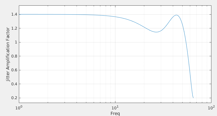
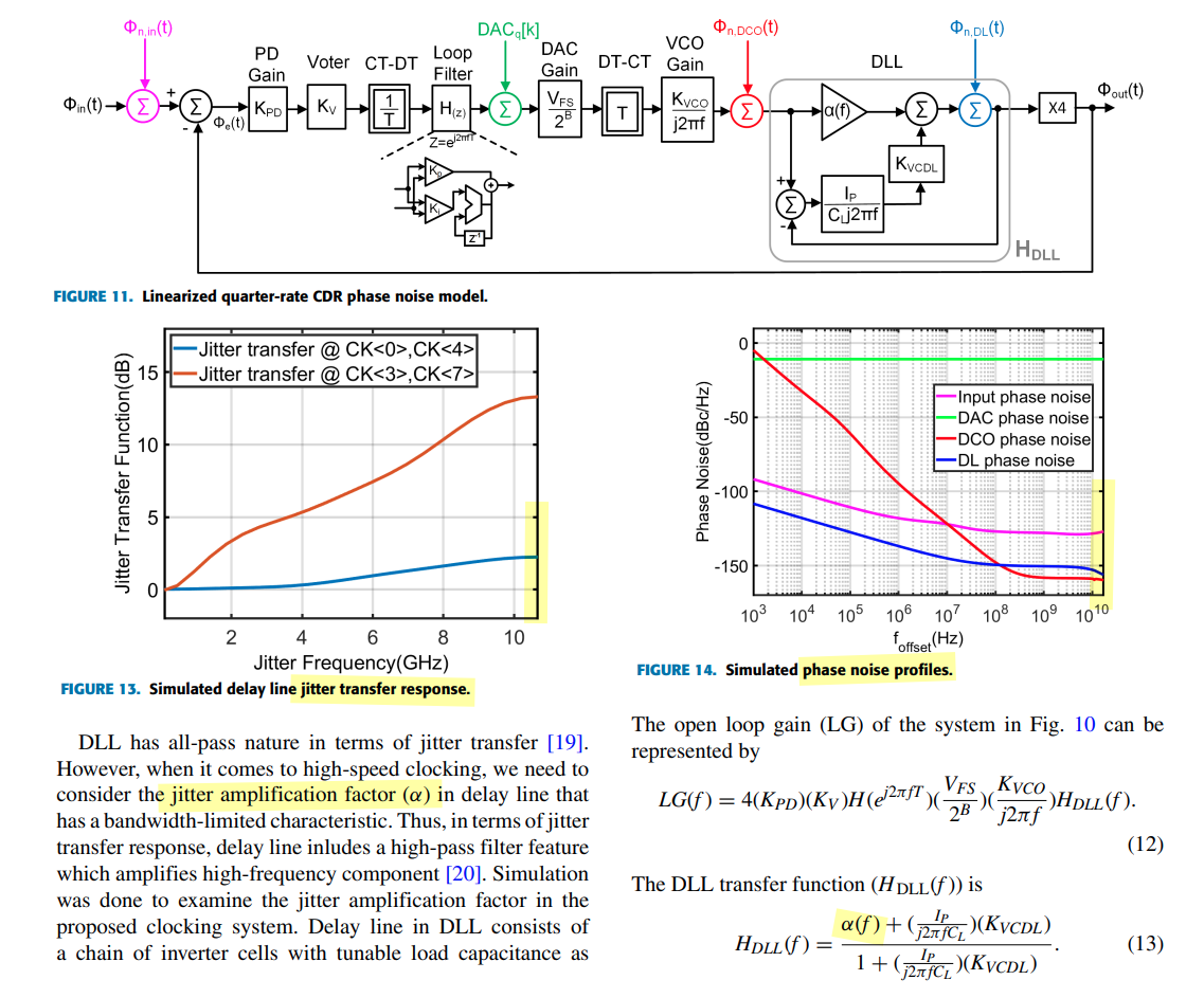
jitter amplification
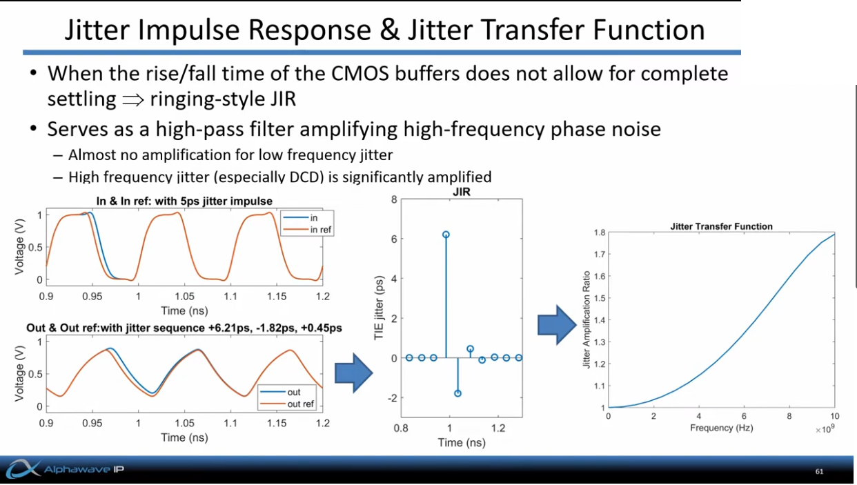
Jitter amplification arises from the transfer characteristic of the clock path, without considering other jitter sources, such as supply noise or thermal noise of the buffer
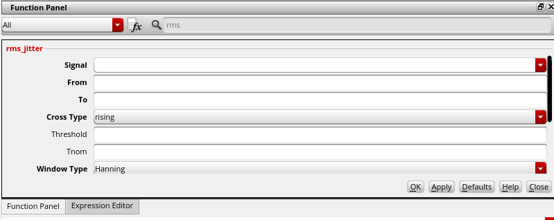
transient noise and rms_jitter function
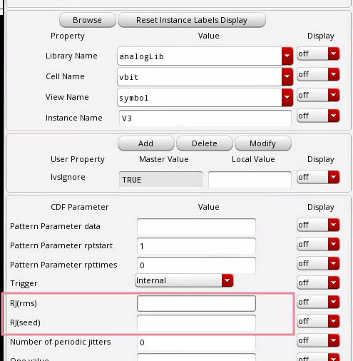
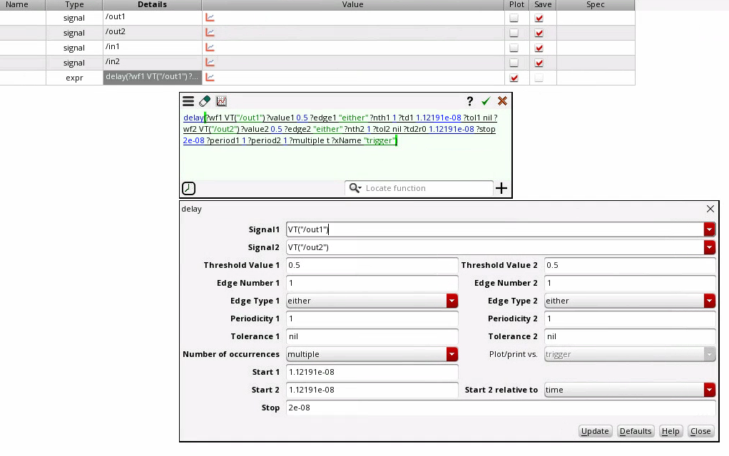
RJ(rms): single Edge or Both Edge?
RJ(seed): what is it?
phase noise method
Directly compare the input phase noise and output phase noise, the input waveform maybe is the PLL output or other clock distribution end point
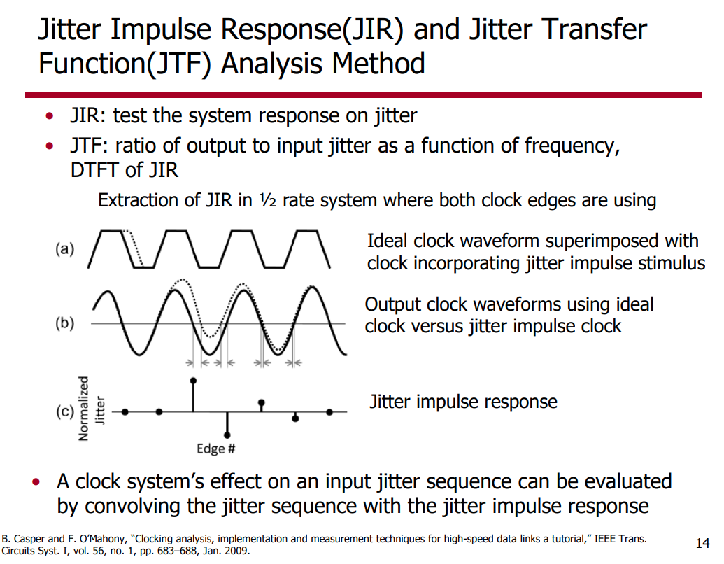
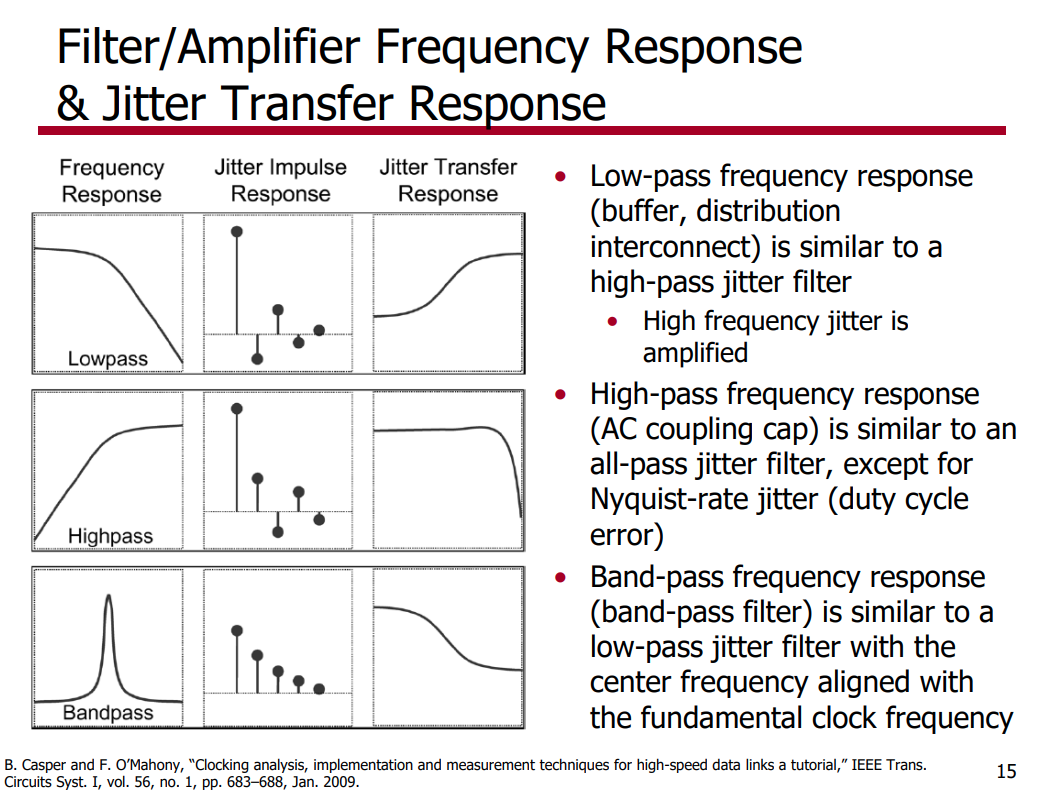
Jitter Impulse Response & Jitter Transfer Function
assuming linear, time-invariant phase response
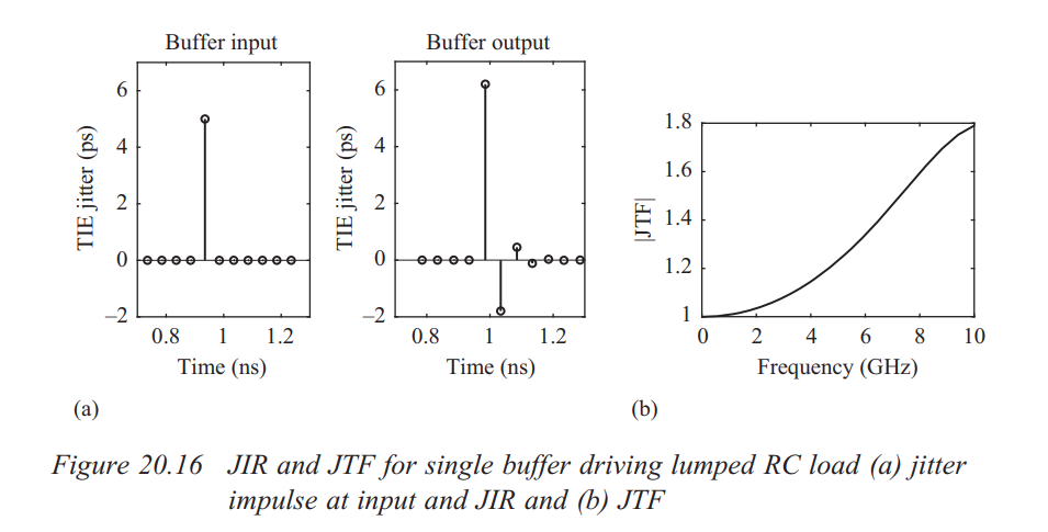
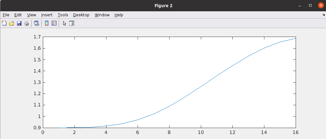
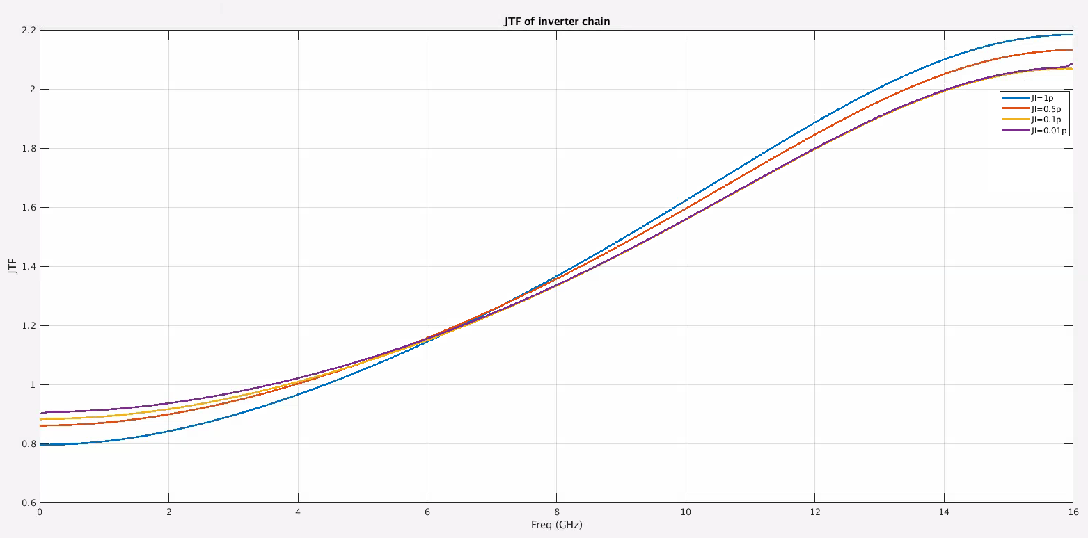
n =5 buffers, fclk = 10GHz
Example
Low Pass Filter
1 | N = 32; |
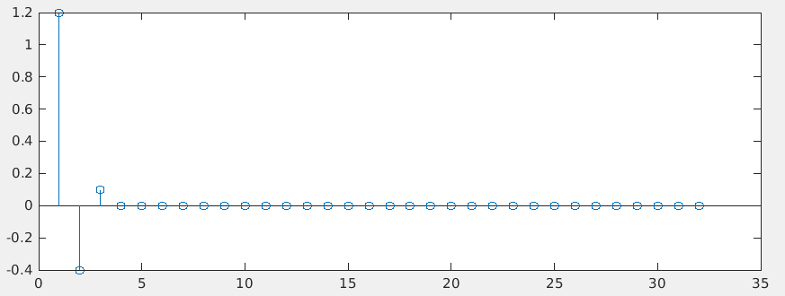
discrete time jitter impulse response
both input and output are discrete time signal, i.e. no sampling in the input, that's why ratio \(1/T_s\) is not in the jtf
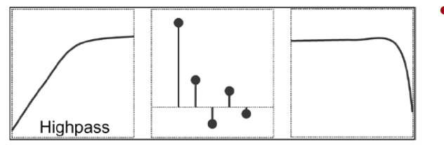
High Pass Filter
1 | N = 128; |
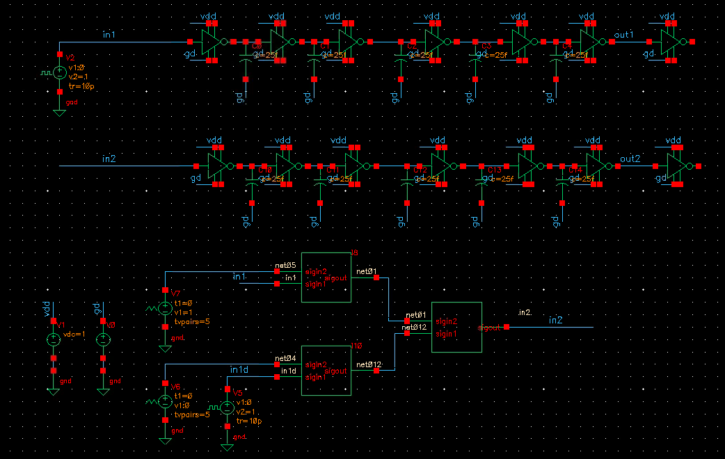
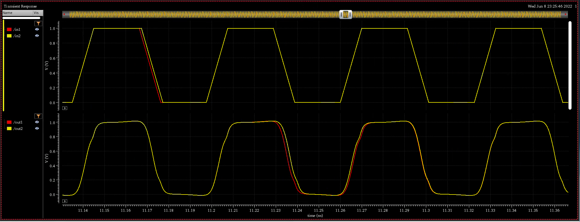
inverter chain
1 | ji = 1e-12; % 1ps |
Phase Noise Integration Limits

Four major noise sources are included in the modeling: Input noise, DAC quantization noise (DAC QN), DCO random noise (DCO RN), and delay line random noise (DL RN).
H. Kang et al., "A 42.7Gb/s Optical Receiver with Digital CDR in 28nm CMOS," 2023 IEEE Radio Frequency Integrated Circuits Symposium (RFIC), San Diego, CA, USA, 2023 [https://ieeexplore.ieee.org/stamp/stamp.jsp?arnumber=10630516]
Reference
Sam Palermo, ECEN 720, Lecture 13 - Forwarded Clock Deskew Circuits
B. Casper and F. O'Mahony, "Clocking Analysis, Implementation and Measurement Techniques for High-Speed Data Links-A Tutorial," in IEEE Transactions on Circuits and Systems I. [https://people.engr.tamu.edu/spalermo/ecen689/clocking_analysis_hs_links_casper_tcas1_2009.pdf]
Phase-Locked Frequency Generation and Clocking : Architectures and Circuits for Modern Wireless and Wireline Systems by Woogeun Rhee (2020, Hardcover)
Mathuranathan Viswanathan, Digital Modulations using Matlab : Build Simulation Models from Scratch
Tony Chan Carusone, University of Toronto, Canada, 2022 CICC Educational Sessions "Architectural Considerations in 100+ Gbps Wireline Transceivers"
X. Mo, J. Wu, N. Wary and T. Chan Carusone, "Design Methodologies for Low-Jitter CMOS Clock Distribution," in IEEE Open Journal of the Solid-State Circuits Society, 2021 [https://ieeexplore.ieee.org/stamp/stamp.jsp?arnumber=9559395]
Modeling Oscillators with Arbitrary Phase Noise Profiles [https://community.cadence.com/cadence_blogs_8/b/rf/posts/modeling-oscillators-with-arbitrary-phase-noise-profiles]
Y. Zhao and B. Razavi, "Phase Noise Integration Limits for Jitter Calculation," 2022 IEEE International Symposium on Circuits and Systems (ISCAS), Austin, TX, USA, 2022 [https://www.seas.ucla.edu/brweb/papers/Conferences/YZ_ISCAS_22.pdf]