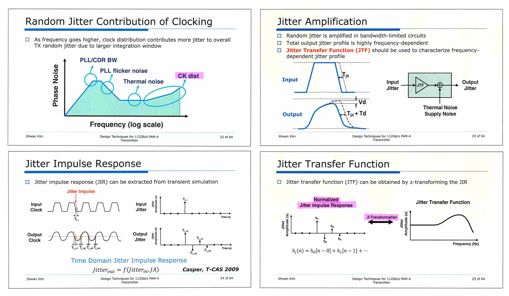
Jitter Amplification
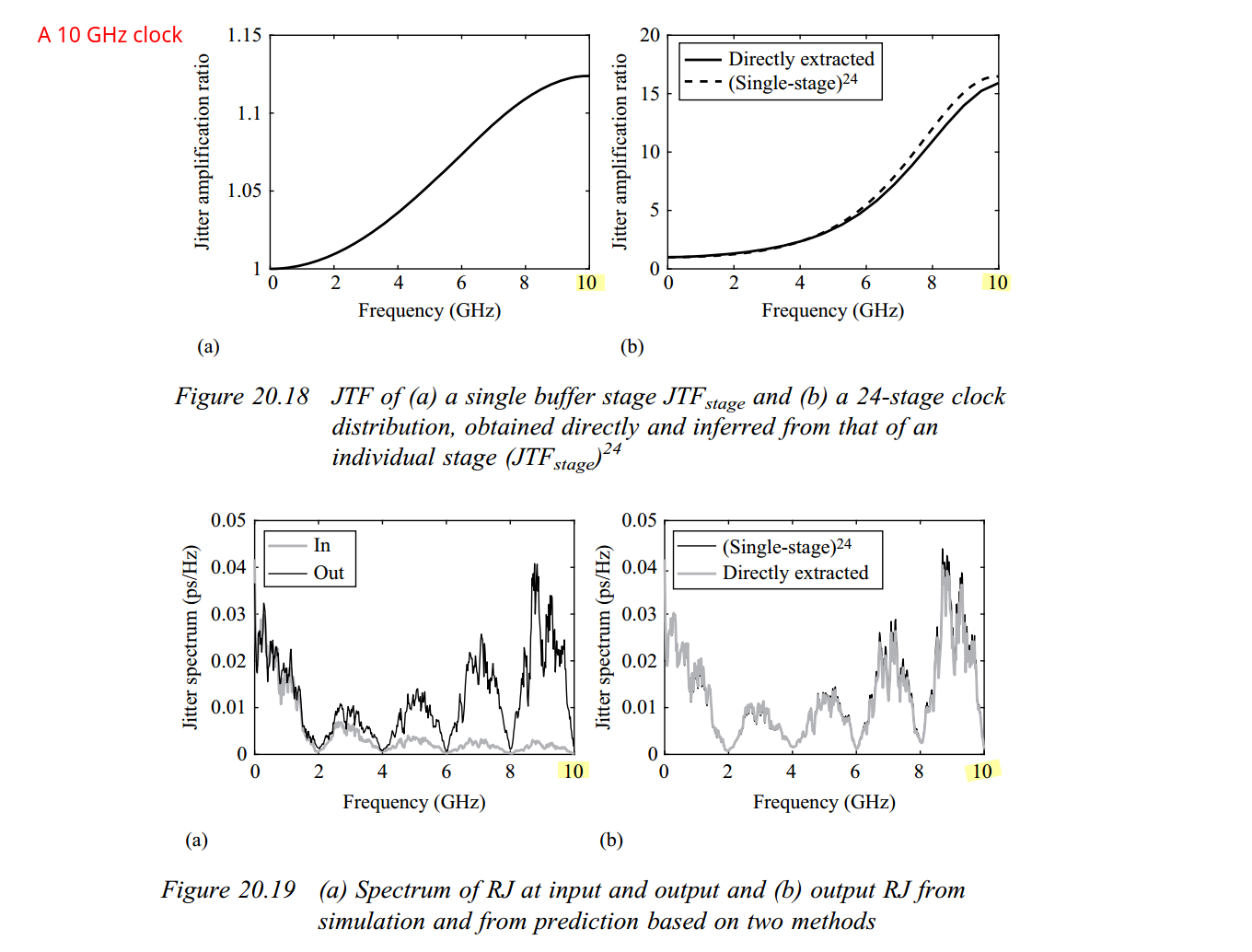
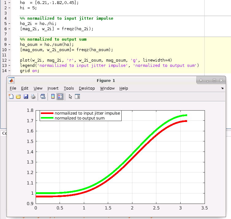
discrete time jitter impulse response (normalized to the input jitter stimulus similar to the procedure used to represent a conventional system impulse response)
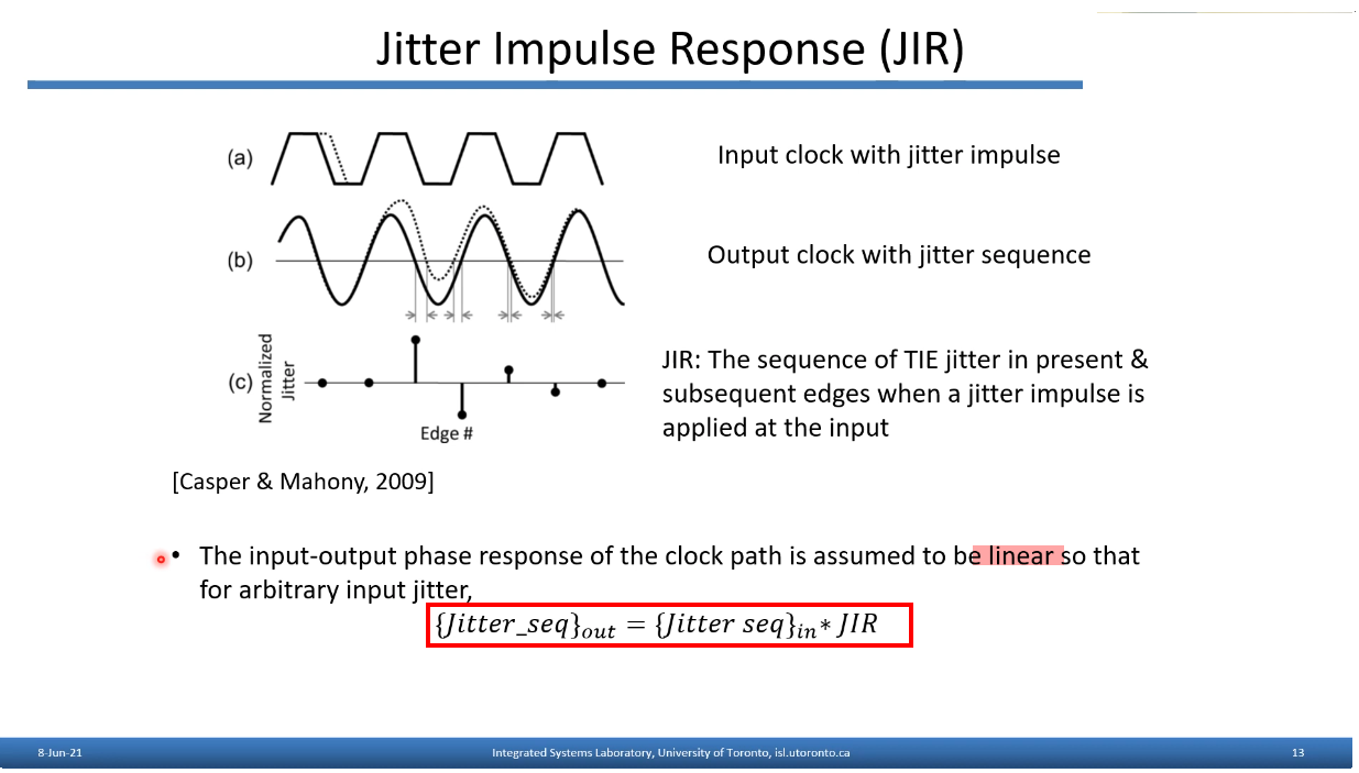
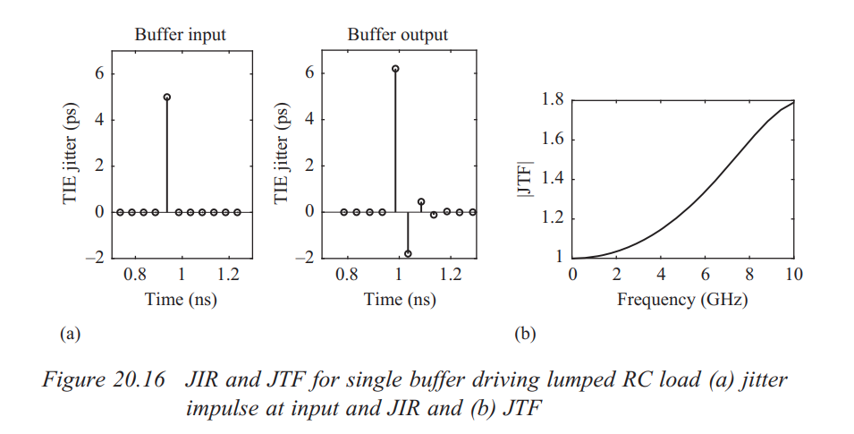
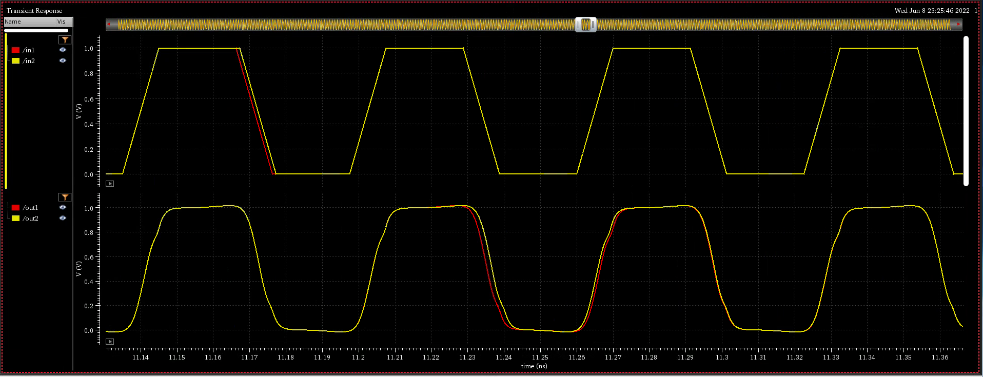
When impulsive jitter is injected into clock distribution circuits (i.e., a small incremental time delay or advance applied to an individual clock edge), it results in jitter in multiple subsequent edges in the output clock
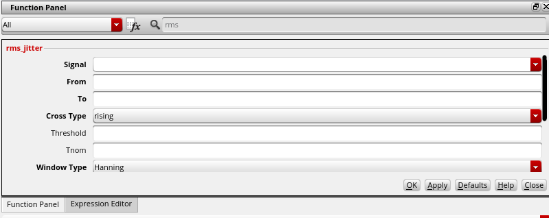
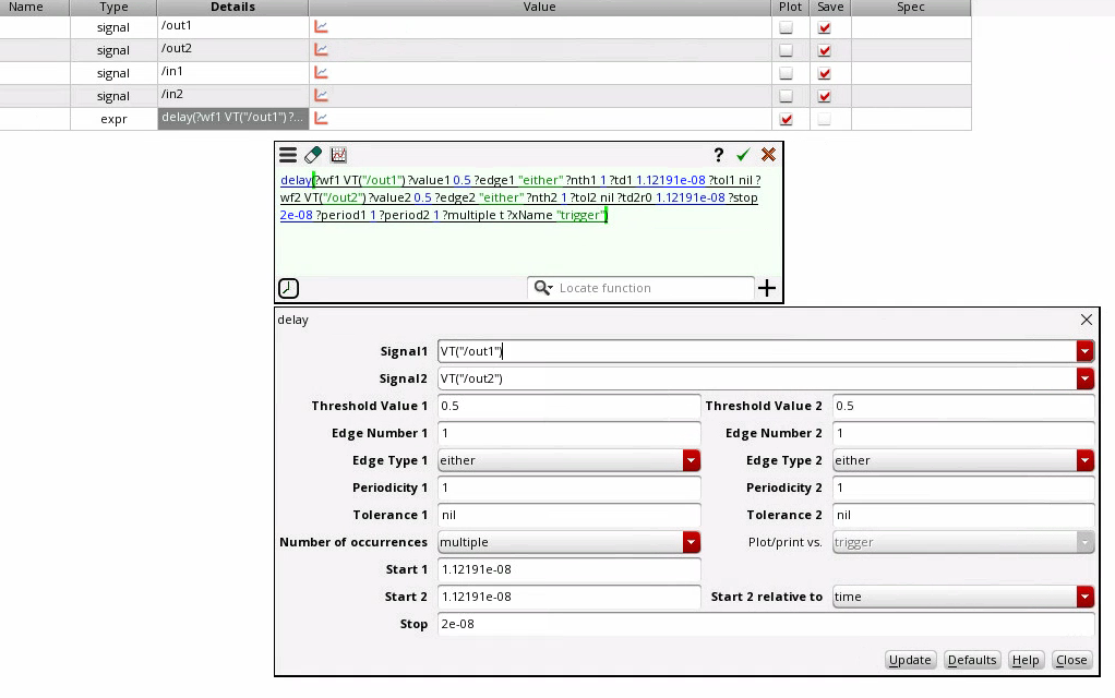
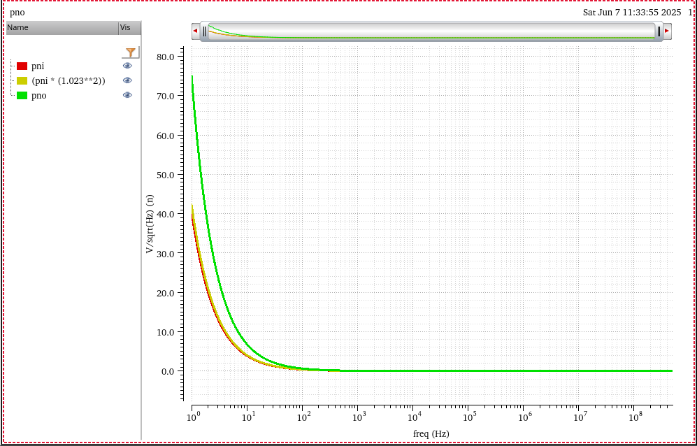
transient noise and rms_jitter function
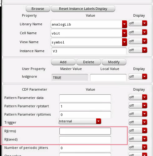
RJ(rms): single Edge or Both Edge?
RJ(seed): what is it?
phase noise method
Directly compare the input phase noise and output phase noise, the input waveform maybe is the PLL output or other clock distribution end point
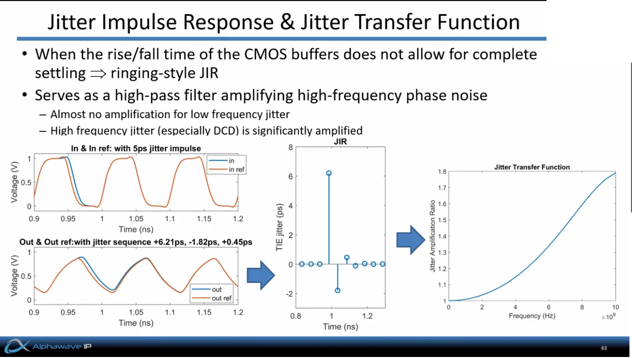
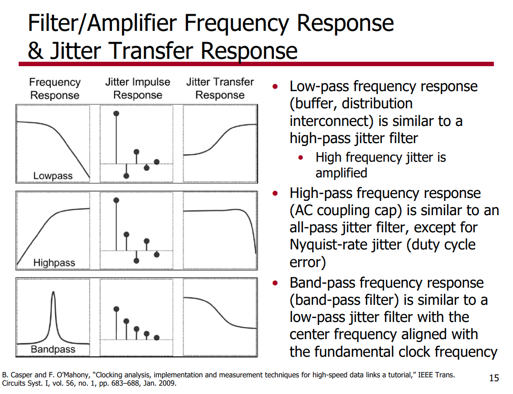
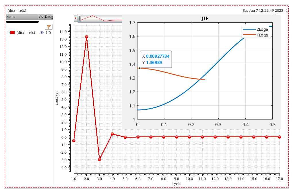
Jitter Impulse Response & Jitter Transfer Function
assuming linear, time-invariant phase response
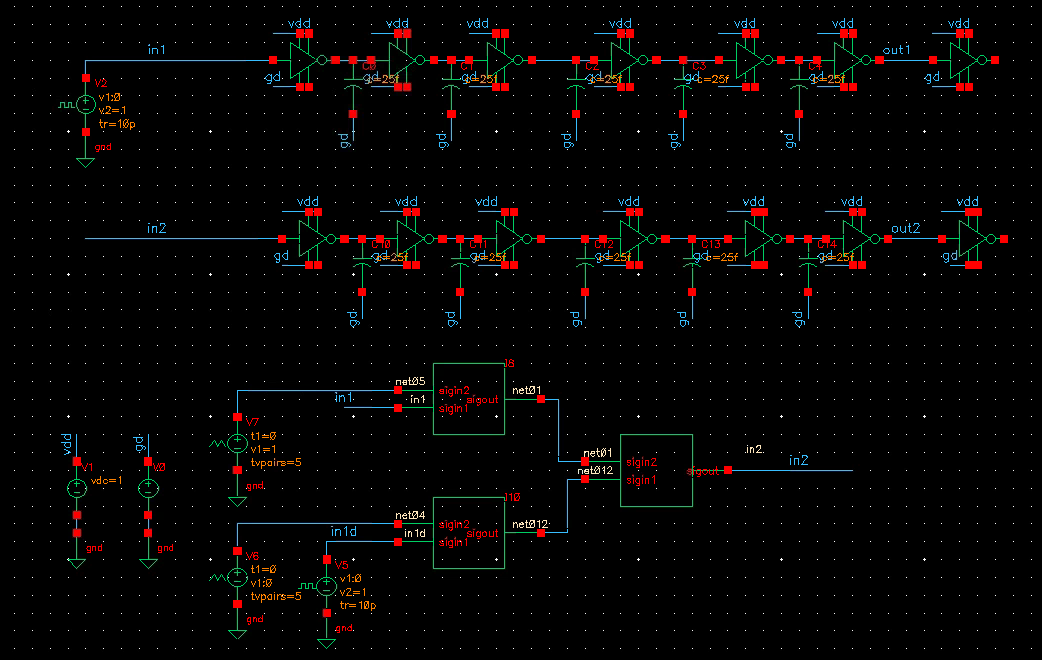
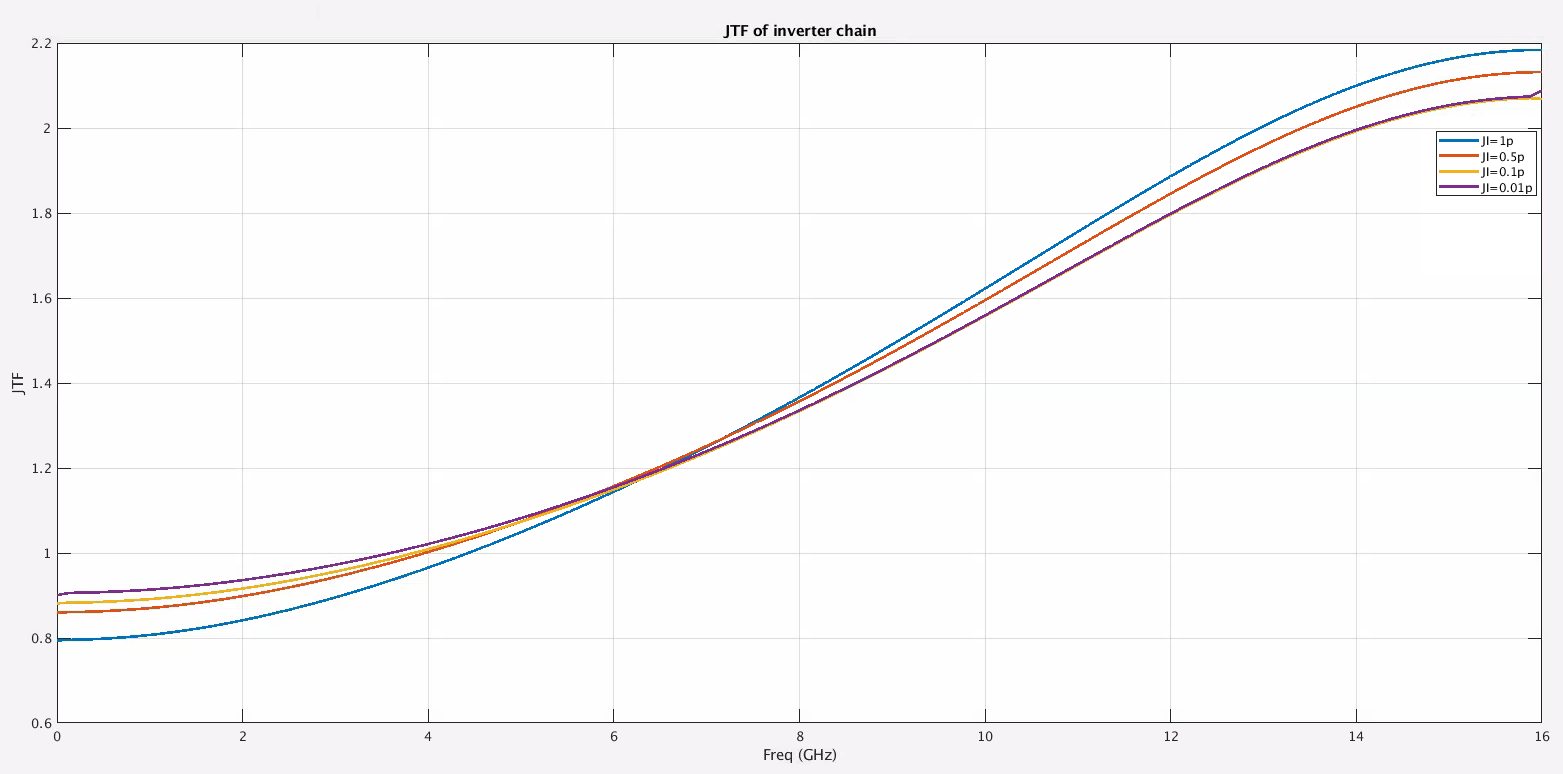
n =5 buffers, fclk = 10GHz
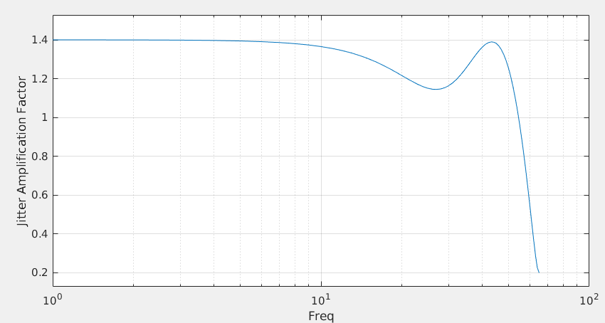
Theoretically, the DC gain of JTF of low pass filter shall be 1. Unfortunately, the gain less than 1 due to numerical error or nonlinearity
Example
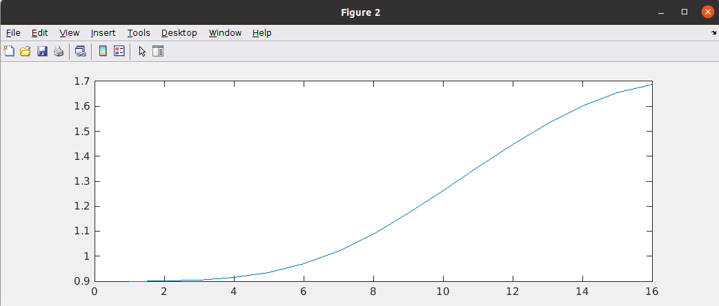
Low Pass Filter
1 | N = 32; |
discrete time jitter impulse response
both input and output are discrete time signal, i.e. no sampling in the input, that's why ratio \(1/T_s\) is not in the jtf
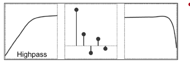
High Pass Filter
1 | N = 128; |
inverter chain
1 | ji = 1e-12; % 1ps |
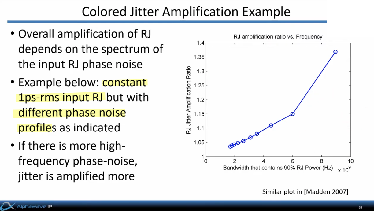
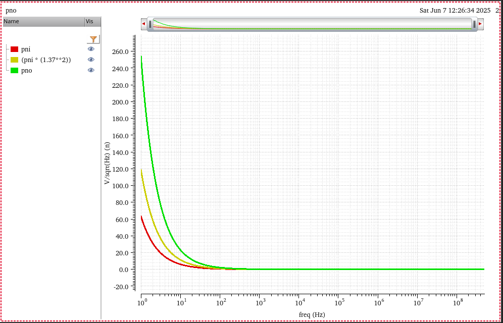
Colored Jitter Amplification
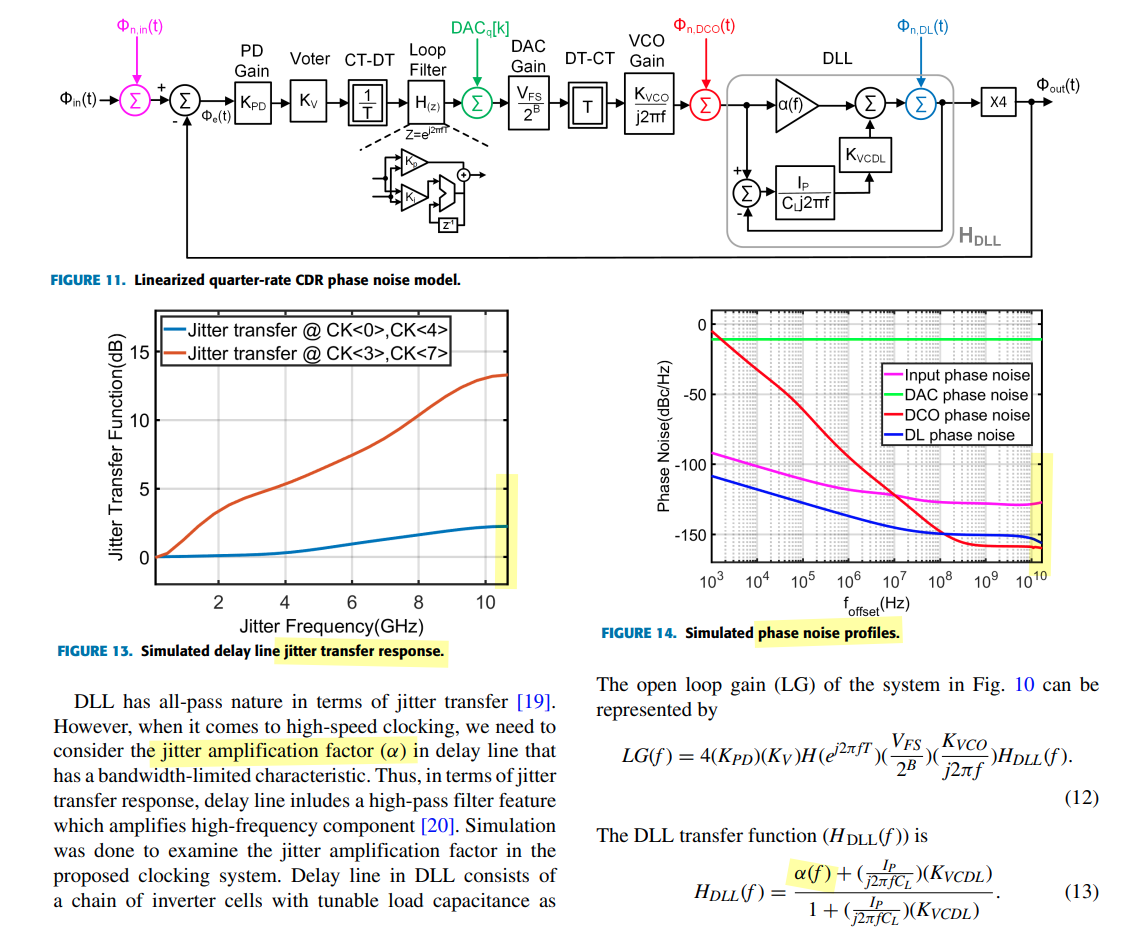
Four major noise sources are included in the modeling: Input noise, DAC quantization noise (DAC QN), DCO random noise (DCO RN), and delay line random noise (DL RN).
H. Kang et al., "A 42.7Gb/s Optical Receiver with Digital CDR in 28nm CMOS," 2023 IEEE Radio Frequency Integrated Circuits Symposium (RFIC), San Diego, CA, USA, 2023 [https://ieeexplore.ieee.org/stamp/stamp.jsp?arnumber=10630516]
Dirac impulse at edge position
Full-rate JTF
Singe edge is using
Half-rate
1 | ji = 10; |
fck = 1GHz
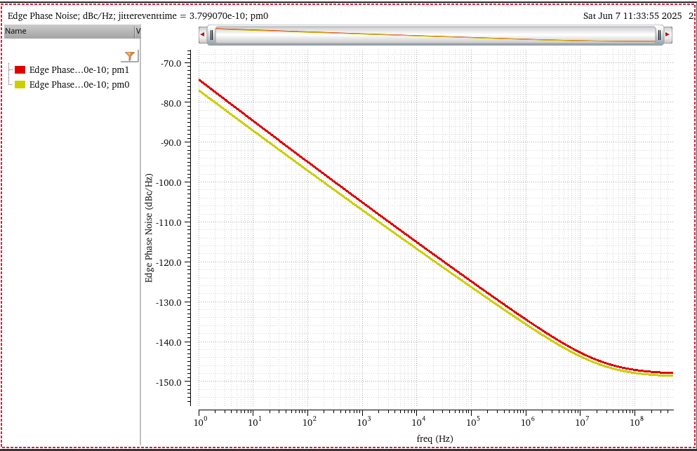
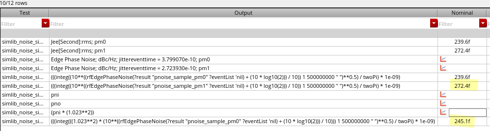
Note: Phase Noise dBc is SSB, that's why we add 10log10(2)
The calculated JTF from JIR is too small compared with Pnoise simualtion
245.1/272.4 = 89.98%
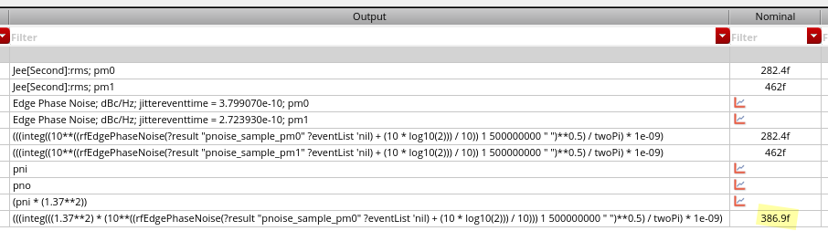
245.1/272.4 = 83.74%
Reference
Sam Palermo, ECEN 720, Lecture 13 - Forwarded Clock Deskew Circuits
B. Casper and F. O'Mahony, "Clocking Analysis, Implementation and Measurement Techniques for High-Speed Data Links-A Tutorial," in IEEE Transactions on Circuits and Systems I. [https://people.engr.tamu.edu/spalermo/ecen689/clocking_analysis_hs_links_casper_tcas1_2009.pdf]
Rhee, W. (2020). Phase-locked frequency generation and clocking : architectures and circuits for modern wireless and wireline systems. The Institution of Engineering and Technology
Mathuranathan Viswanathan, Digital Modulations using Matlab : Build Simulation Models from Scratch
Tony Chan Carusone, University of Toronto, Canada, 2022 CICC Educational Sessions "Architectural Considerations in 100+ Gbps Wireline Transceivers"
X. Mo, J. Wu, N. Wary and T. Chan Carusone, "Design Methodologies for Low-Jitter CMOS Clock Distribution," in IEEE Open Journal of the Solid-State Circuits Society, 2021 [https://ieeexplore.ieee.org/stamp/stamp.jsp?arnumber=9559395]
Y. Zhao and B. Razavi, "Phase Noise Integration Limits for Jitter Calculation," 2022 IEEE International Symposium on Circuits and Systems (ISCAS), Austin, TX, USA, 2022 [https://www.seas.ucla.edu/brweb/papers/Conferences/YZ_ISCAS_22.pdf]
Thomas Toifl. TWEPP 2012. Low-power High-Speed CMOS I/Os: Design Challenges and Solutions [https://indico.cern.ch/event/170595/contributions/266344/attachments/212179/297391/twepp_sept2012_final_v2.pdf]
Ganesh Balamurugan and Naresh Shanbhag, "Modeling and mitigation of jitter in multiGbps source-synchronous I/O links," Proceedings 21st International Conference on Computer Design, San Jose, CA, USA, 2003, pp. 254-260, doi: 10.1109/ICCD.2003 [https://shanbhag.ece.illinois.edu/publications/ganesh-ICCD2203.pdf]
Balamurugan, G. & Casper, Bryan & Jaussi, James & Mansuri, Mozhgan & O'Mahony, Frank & Kennedy, Joseph. (2009). Modeling and Analysis of High-Speed I/O Links. Advanced Packaging, IEEE Transactions on. [https://sci-hub.se/10.1109/TADVP.2008.2011366]
Jihwan Kim, ISSCC2019 F5: Design Techniques for a 112Gbs PAM-4 Transmitter