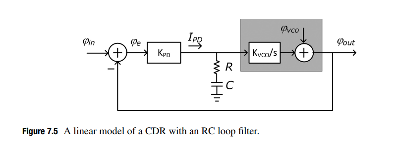
Linear model of the CDR
condition:
Linear model of the CDR is used in a frequency lock condition and is approaching to achieve phase lock
Using this model, the power spectral density (PSD) of jitter in the recovered clock \(S_{out}(f)\) is \[ S_{out}(f)=|H_T(f)|^2S_{in}(f)+|H_G(f)|^2S_{VCO}(f) \] Here, we assume \(\varphi_{in}\) and \(\varphi_{VCO}\) are uncorrelated as they come from independent sources.
Jitter Transfer
\[ H_T(s) = \frac{\varphi_{out}(s)}{\varphi_{in}(s)}|_{\varphi_{vco}=0}=\frac{K_{PD}K_{VCO}R_s+\frac{K_{PD}K_{VCO}}{C}}{s^2+K_{PD}K_{VCO}R_s+\frac{K_{PD}K_{VCO}}{C}} \]
Using below notation \[\begin{align} \omega_n^2=\frac{K_{PD}K_{VCO}}{C} \\ \xi=\frac{K_{PD}K_{VCO}}{2\omega_n^2} \end{align}\]
We can rewrite transfer function as follows \[ H_T(s)=\frac{2\xi\omega_n s+\omega_n^2}{s^2+2\xi \omega_n s+\omega_n^2} \]
The jitter transfer represents a low-pass filter whose magnitude is around 1 (0 dB) for low jitter frequencies and drops at 20 dB/decade for frequencies above \(\omega_n\)
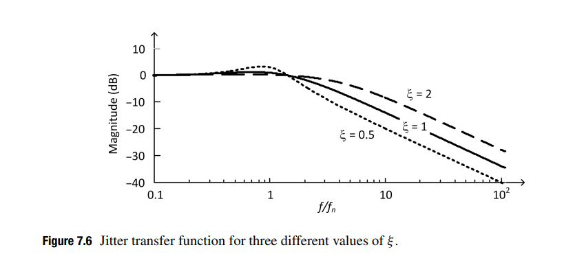
- the recovered clock track the low-frequency jitter of the input data
- the recovered clock DONT track the high-frequency jitter of the input data
The recovered clock does not suffer from high-frequency jitter even though the input signal may contain high-frequency jitter, which will limit the CDR tolerance to high-frequency jitter.
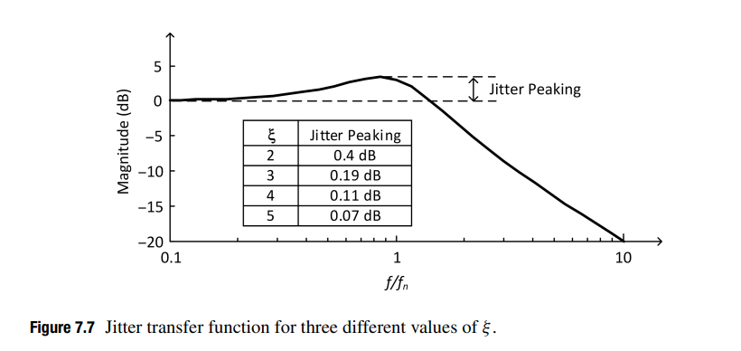
Jitter Peaking in Jitter Transfer Function
The peak, slightly larger than 1 (0dB) implies that jitter will be amplified at some frequencies in the CDR, producing a jitter amplitude in the recovered clock, and thus also in the recovered data, that is slightly larger than the jitter amplitude in the input data.
This is certainly undesirable, especially in applications such as repeaters.
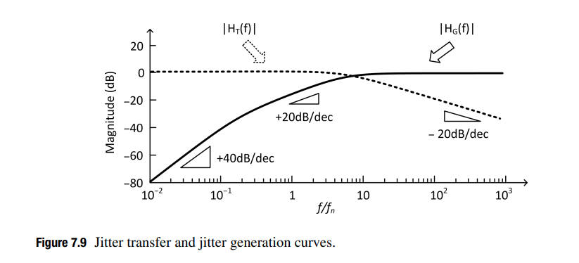
Jitter Generation
If the input data to the CDR is clean with no jitter, i.e., \(\varphi_{in}=0\), the jitter of the recovered clock comes directly from the VCO jitter. The transfer function that relates the VCO jitter to the recovered clock jitter is known as jitter generation. \[ H_G(s)=\frac{\varphi_{out}}{\varphi_{VCO}}|_{\varphi_{in}=0}=\frac{s^2}{s^2+2\xi \omega_n s+\omega_n^2} \] Jitter generation is high-pass filter with two zeros, at zero frequency, and two poles identical to those of the jitter transfer function
Jitter Tolerance
To quantify jitter tolerance, we often apply a sinusoidal jitter of a fixed frequency to the CDR input data and observe the BER of the CDR
The jitter tolerance curve DONT capture a CDR's true tolerance to random jitter. Because we are applying "sinusoidal" jitter, which is deterministic signal.
We can deal only with the jitter's amplitude and frequency instead of
the PSD of the jitter thanks to deterministic sinusoidal jitter signal.
\[
JTOL(f) = \left | \varphi_{in}(f) \right |_{\text{pp-max}} \quad
\text{for a fixed BER}
\] Where the subscript \(\text{pp-max}\) indicates the maximum
peak-to-peak amplitude. We can further expand this equation as follows
\[
JTOL(f)=\left| \frac{\varphi_{in}(f)}{\varphi_{e}(f)} \right| \cdot
|\varphi_e(f)|_{pp-max}
\] 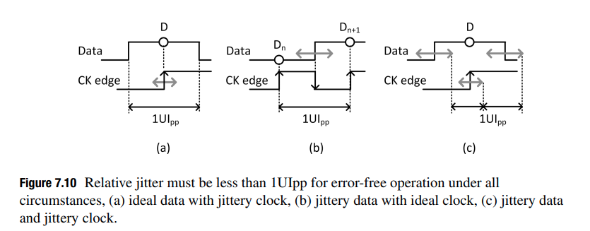
Relative jitter, \(\varphi_e\) must be less than 1UIpp for error-free operation
In an ideal CDR, the maximum peak-to-peak amplitude of \(|\varphi_e(f)|\) is 1UI, i.e.,\(|\varphi_e(f)|_{pp-max}=1UI\)
Accordingly, jitter tolerance can be expressed in terms of the number
of UIs as \[
JTOL(f)=\left| \frac{\varphi_{in}(f)}{\varphi_{e}(f)} \right|\quad
\text{[UI]}
\] Given the linear CDR model, we can write \[
JTOL(f)=\left| 1+\frac{K_{PD}K_{VCO}H_{LF}(f)}{j2\pi f} \right|\quad
\text{[UI]}
\] Expand \(H_{LF}(f)\) for the
CDR, we can write \[
JTOL(f)=\left| 1-2\xi j \left(\frac{f_n}{f}\right) -
\left(\frac{f_n}{f}\right)^2 \right|\quad \text{[UI]}
\] 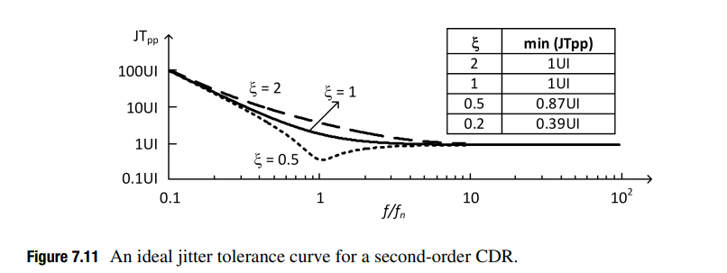
At frequencies far below and above the natural frequency, the jitter tolerance can be approximated by the following \[ JTOL(f) = \left\{ \begin{array}{cl} \left(\frac{f_n}{f}\right)^2 & : \ f\ll f_n \\ 1 & : \ f\gg f_n \end{array} \right. \]
- the jitter tolerance at very high jitter
frequencies is limited to 1UIpp
- This is consistent with that the recovered clock does not track the high-frequency jitter, limiting the maximum peak-to-peak deviation of the data edge from its nominal position to 1UI
- The circumstance, (b) jittery data with ideal clock
- the jitter tolerance is increased at 40dB/decade for jitter
frequencies below \(f_c\)
- This is consistent with our obervation earlier that the recovered clock better tracks data jitter at lower jitter frequencies
- Equivalently, the data edge and the clock edge move together in the same direction. As a result, the relative jitter between the data and the clock remains small, i.e., below 1UI peak-to-peak
- The circumstance, (c) jittery data and jittery clock
OJTF
Concepts of JTF and OJTF
Simplified Block Diagram of a Clock-Recovery PLL 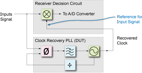
Jitter Transfer Function (JTF)
- Input Signal Versus Recovered Clock
- JTF, by jitter frequency, compares how much input signal jitter is
transferred to the output of a clock-recovery's PLL (recovered
clock)
- Input signal jitter that is within the clock recovery PLL's loop bandwidth results in jitter that is faithfully transferred (closed-loop gain) to the clock recovery PLL's output signal. JTF in this situation is approximately 1.
- Input signal jitter that is outside the clock recovery PLL's loop bandwidth results in decreasing jitter (open-loop gain) on the clock recovery PLL's output, because the jitter is filtered out and no longer reaches the PLL's VCO
Observed Jitter Transfer Function
- Input Signal Versus Sampled Signal
- OJTF compares how much input signal jitter is transferred to the
output of a receiver's decision making circuit as
effected by a clock recovery's PLL. As the recovered clock is the
reference for detecting the input signal
- Input signal jitter that is within the clock recovery PLL's loop bandwidth results in jitter on the recovered clock which reduces the amount of jitter that can be detected. The input signal and clock signal are closer in phase
- Input signal jitter that is outside the clock recovery PLL's loop bandwidth results in reduced jitter on the recovered clock which increases the amount of jitter that can be detected. The input signal and clock signal are more out of phase. Jitter that is on both the input and clock signals can not detected or is reduced
JTF and OJTF for 1st Order PLLs
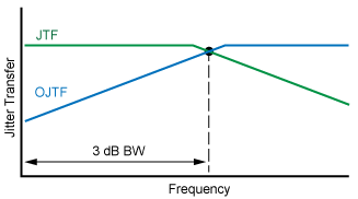
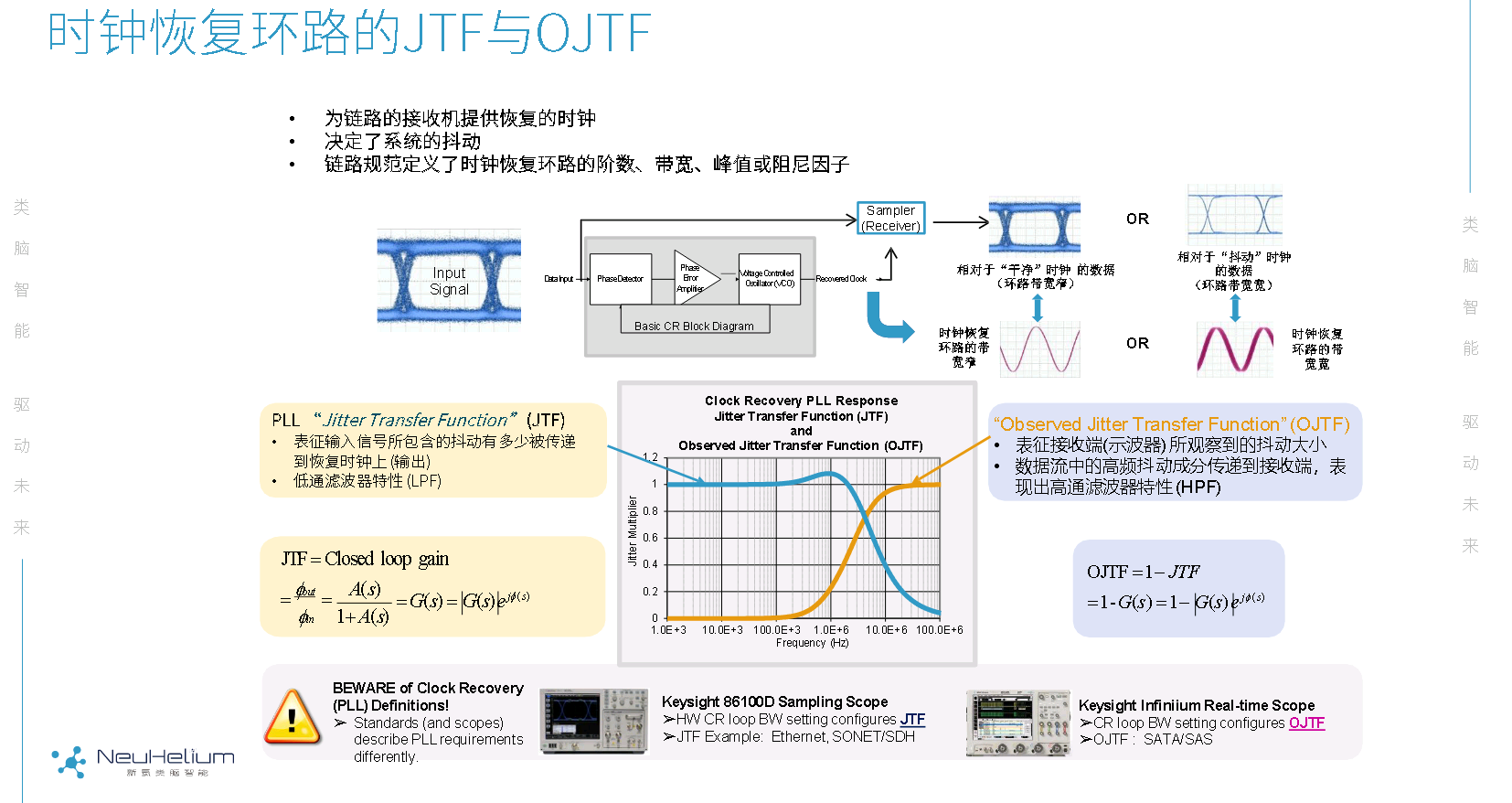
The observed jitter is a complement to the PLL jitter transfer response OJTF=1-JTF (Phase matters!)
OTJF gives the amount of jitter which is tracked and therefore not observed at the output of the CDR as a function of the jitter rate applied to the input.
Jitter Measurement
\[ J_{\text{measured}} = JTF_{\text{DUT}} \cdot OJTF_{\text{instrument}} \] The combination of the OJTF of a jitter measurement device and the JTF of the clock generator under test gives the measured jitter as a function of frequency.
For example, a clock generator with a type 1, 1st order PLL measured with a jitter measurement device employing a golden PLL is \[ J_{\text{measured}} = \frac{\omega_1}{s+\omega_1}\frac{s}{s+\omega_2} \]
Accurate measurement of the clock JTF requires that the OJTF cutoff of the jitter measurement be significantly below that of the clock JTF and that the measurement is compensated for the instrument's OJTF.
The overall response is a band pass filter because the clock JTF is low pass and the jitter measurement device OJTF is high pass.
The compensation for the instrument OJTF is performed by measuring the jitter of the reference clock at each jitter rate being tested and comparing the reference jitter with the jitter measured at the output of the DUT.
The lower the cutoff frequency of the jitter measurement device the better the accuracy of the measurement will be.
The cutoff frequency is limited by several factors including the phase noise of the DUT and measurement time.
Digital Sampling Oscilloscope
How to analyze jitter:
- TIE (Time Interval Error) track
- histogram
- FFT
TIE track provides a direct view of how the phase of the clock evolves over time.
histogram provides valuable information about the long term variations in the timing.
FFT allows jitter at specific rates to be measured down to the femto-second range.
Maintaining the record length at a minimum of \(1/10\) of the inverse of the PLL loop bandwidth minimizes the response error
reference
Dalt, Nicola Da and Ali Sheikholeslami. “Understanding Jitter and Phase Noise: A Circuits and Systems Perspective.” (2018).
neuhelium, 抖动、眼图和高速数字链路分析基础 URL: http://www.neuhelium.com/ueditor/net/upload/file/20200826/DSOS254A/03.pdf
Keysight JTF & OJTF Concepts, https://rfmw.em.keysight.com/DigitalPhotonics/flexdca/FlexPLL-UG/Content/Topics/Quick-Start/jtf-pll-theory.htm?TocPath=Quick%20Start%7C_____4
Complementary Transmitter and Receiver Jitter Test Methodlogy, URL: https://www.ieee802.org/3/bm/public/mar14/ghiasi_01_0314_optx.pdf
SerDesDesign.com CDR_BangBang_Model URL: https://www.serdesdesign.com/home/web_documents/models/CDR_BangBang_Model.pdf
M. Schnecker, Jitter Transfer Measurement in Clock Circuits, LeCroy Corporation, DesignCon 2009. URL: http://cdn.teledynelecroy.com/files/whitepapers/designcon2009_lecroy_jitter_transfer_measurement_in_clock_circuits.pdf