Clock Distribution Techniques
Clocking Structures
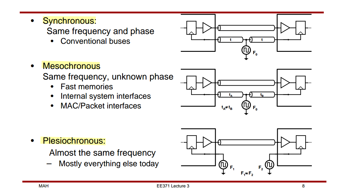
Mark Horowitz, Lecture 6 Clocked Elements [https://web.stanford.edu/class/archive/ee/ee371/ee371.1066/lectures/lect_06.pdf]
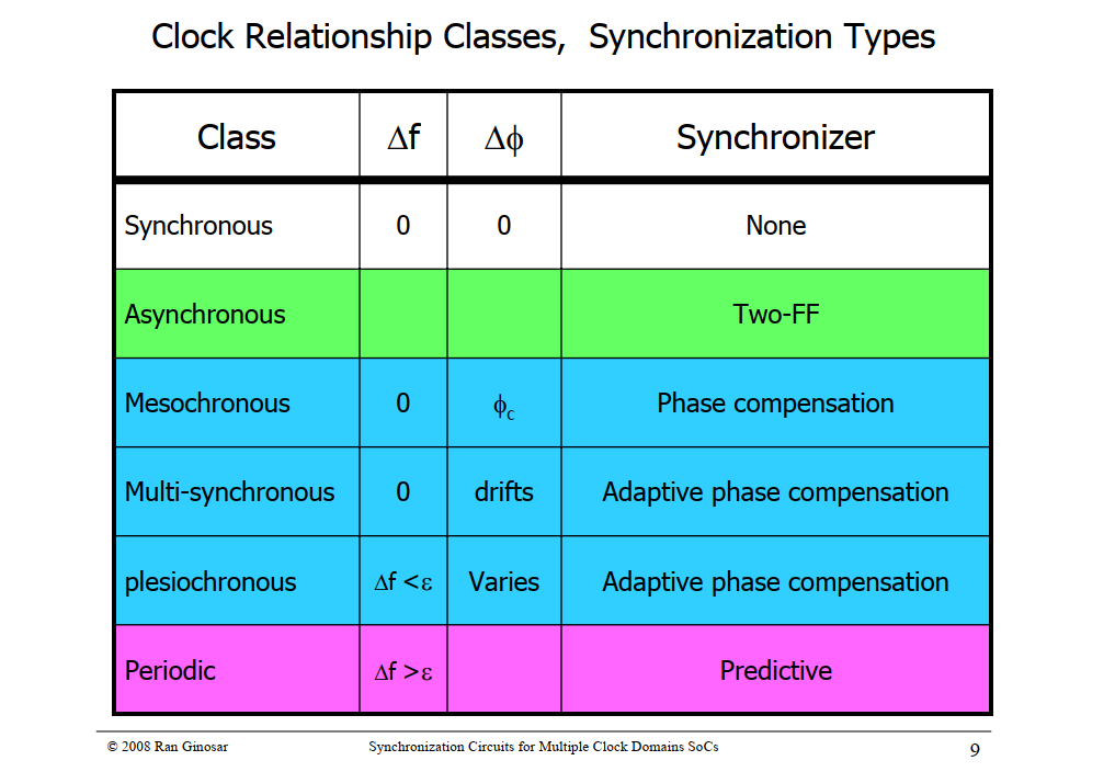
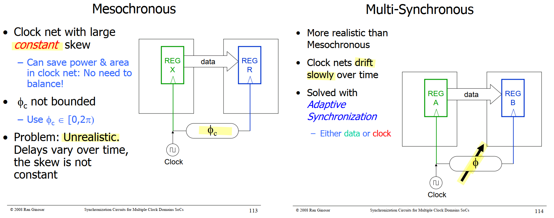
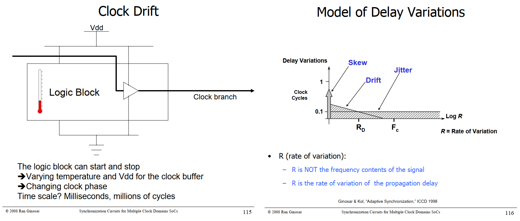
Ran Ginosar, ISCAS2008 Tutorial-4: Synchronization Circuits for Multiple Clock Domain SoCs
Synchronous, Mesochronous, Plesiochronous
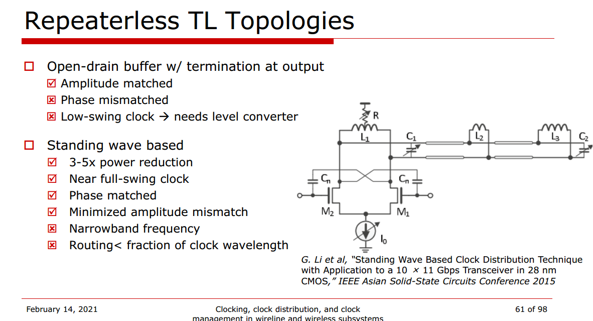
Standing Wave Based Clock Distribution Technique
G. Li, W. Lee, D. Cui, B. Zhang, A. Momtaz and J. Cao, "Standing wave based clock distribution technique with application to a 10 × 11 Gbps transceiver in 28 nm CMOS," 2015 IEEE Asian Solid-State Circuits Conference (A-SSCC), Xiamen, China, 2015, pp. 1-4 [https://sci-hub.se/10.1109/ASSCC.2015.7387451]
T. Ali et al., "6.4 A 180mW 56Gb/s DSP-Based Transceiver for High Density IOs in Data Center Switches in 7nm FinFET Technology," 2019 IEEE International Solid-State Circuits Conference - (ISSCC), San Francisco, CA, USA, 2019, pp. 118-120 [https://sci-hub.se/10.1109/ISSCC.2019.8662523]
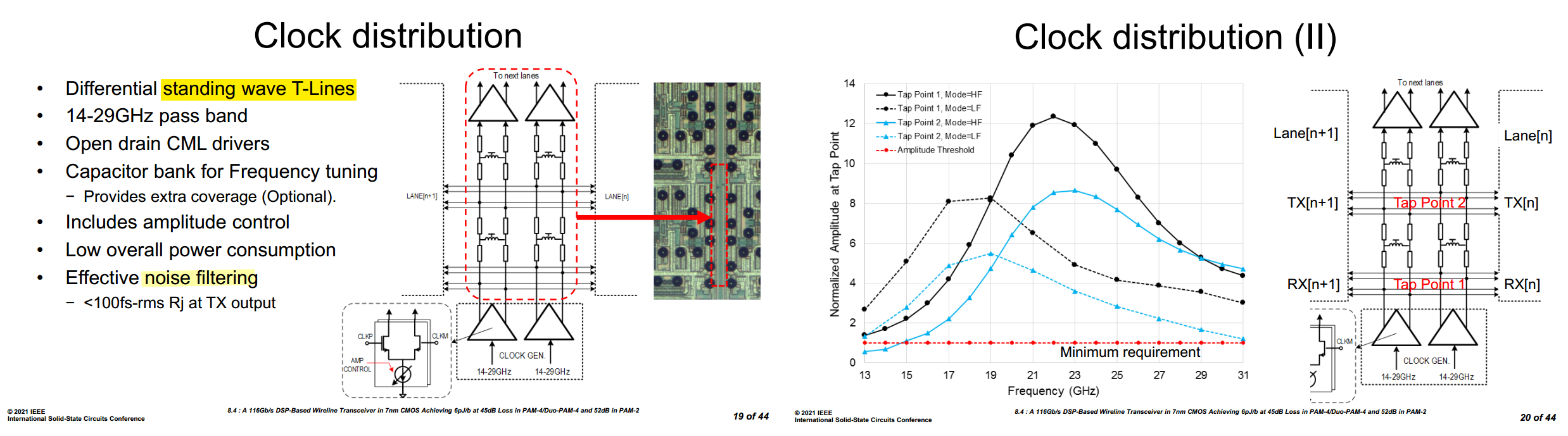
M. -A. LaCroix et al., "8.4 A 116Gb/s DSP-Based Wireline Transceiver in 7nm CMOS Achieving 6pJ/b at 45dB Loss in PAM-4/Duo-PAM-4 and 52dB in PAM-2," 2021 IEEE International Solid-State Circuits Conference (ISSCC), San Francisco, CA, USA, 2021, pp. 132-134 [https://sci-hub.ru/10.1109/ISSCC42613.2021.9366030]
hai-kun,『讲电路』传输线和驻波在时钟分布网络中的应用 [https://zhuanlan.zhihu.com/p/30055007]
TODO 📅
Inductive-Loaded Clock Distribution Technique
T. Shibasaki et al., "3.5 A 56Gb/s NRZ-electrical 247mW/lane serial-link transceiver in 28nm CMOS," 2016 IEEE International Solid-State Circuits Conference (ISSCC), San Francisco, CA, USA, 2016, pp. 64-65 [https://sci-hub.se/10.1109/ISSCC.2016.7417908]
TODO 📅
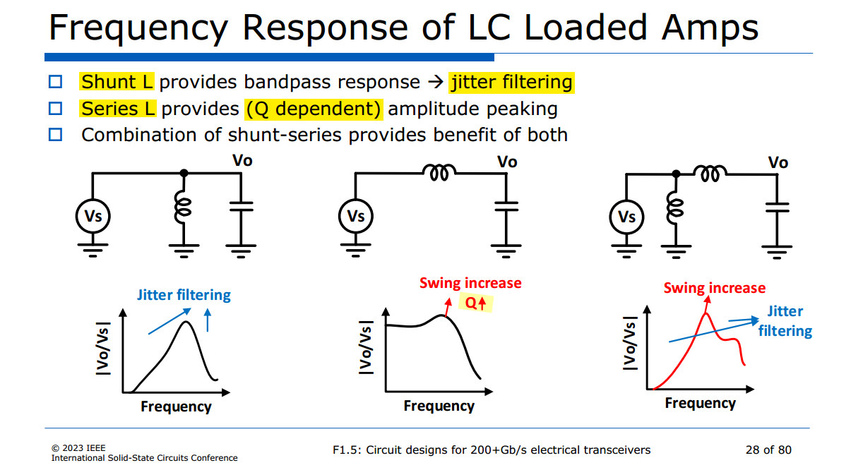
LC Loaded Amps
Cascaded PLLs
Chembiyan T, A General Theory of Cascaded PLL Design [link]
Nicola Da Dalt, ISSCC 2012 T5: JITTER basic and advanced concepts, statistics and applications
—. ESSCIRC 2019 Tutorials: Jitter in Wireline and Data Converter Applications [https://youtu.be/aapkfCeHTrQ]
To understand the impact of the clock jitter on the performance of a wireline system, the transfer functions of the PLL in the transmitter side and the CDR loop in the receiver should be taken into consideration
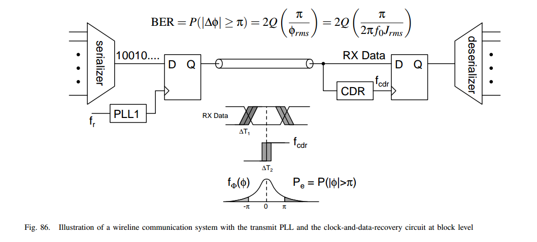
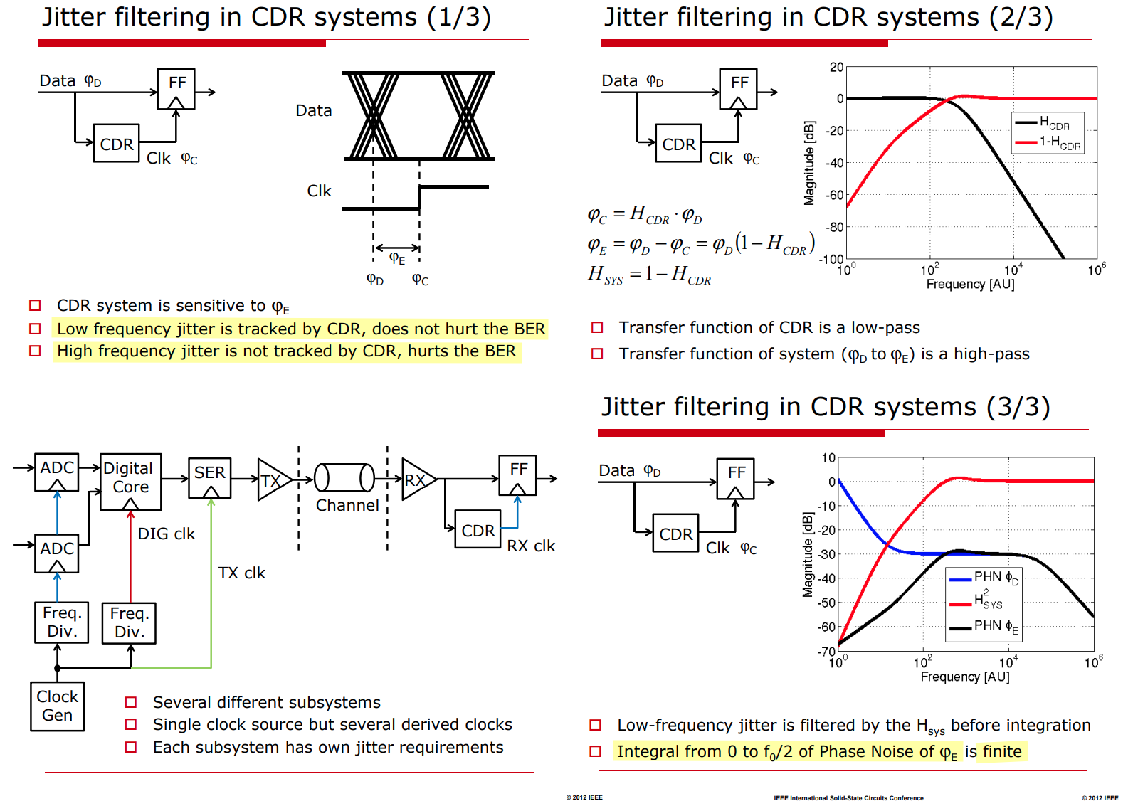
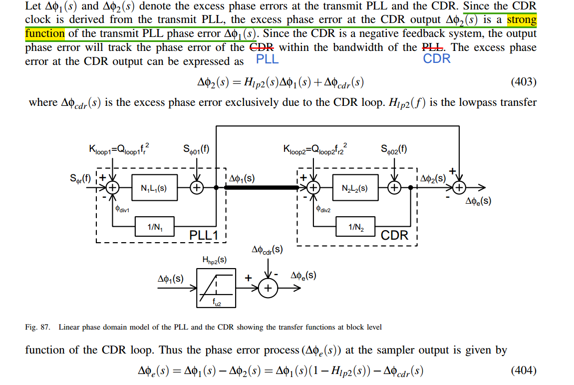
the minimum jitter occurs at the point where the transmit PLL UGB is minimum and the CDR UGB is maximized
- the net rms jitter that impacts the performance of a wireline transceiver is much lower than the rms jitter of the transmit PLL
- the jitter requirements of the transmit PLL on the wireline system is much more relaxed compared to the wireless transceiver
Frequency Dividers
Xu, Haojie & Luo, Bao & Jin, Gaofeng & Feng, Fei & Guo, Huanan & Gao, Xiang & Deo, Anupama. (2022). A Flexible 0.73-15.5 GHz Single LC VCO Clock Generator in 12 nm CMOS. IEEE Transactions on Circuits and Systems II: Express Briefs. 69. 4238 - 4242. [https://www.researchgate.net/publication/382240520_A_Flexible_073-155_GHz_Single_LC_VCO_Clock_Generator_in_12_nm_CMOS]
TODO 📅
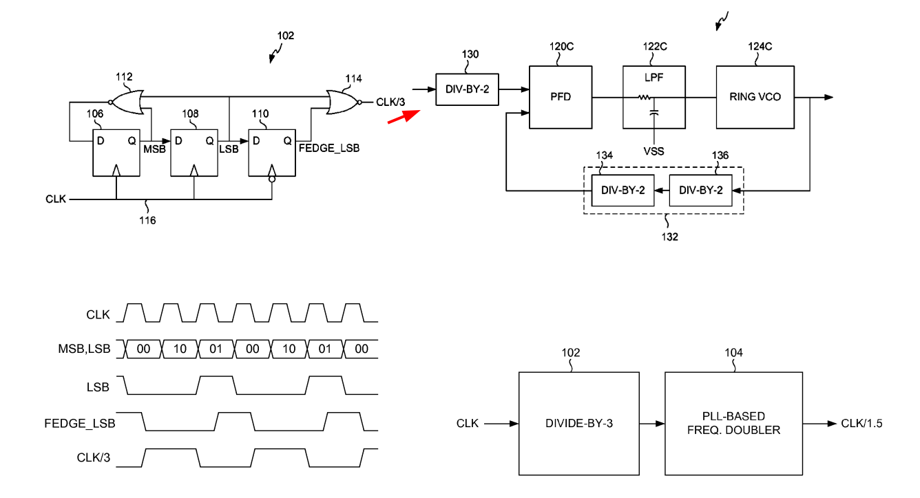
divide-by-1.5 circuit
US9065449B2 High-speed divide-by-1.5 circuit with 50 percent duty cycle [https://patents.google.com/patent/US9065449B2]
divide-by-3 circuit + frequency doubler circuit
Deterministic Jitter
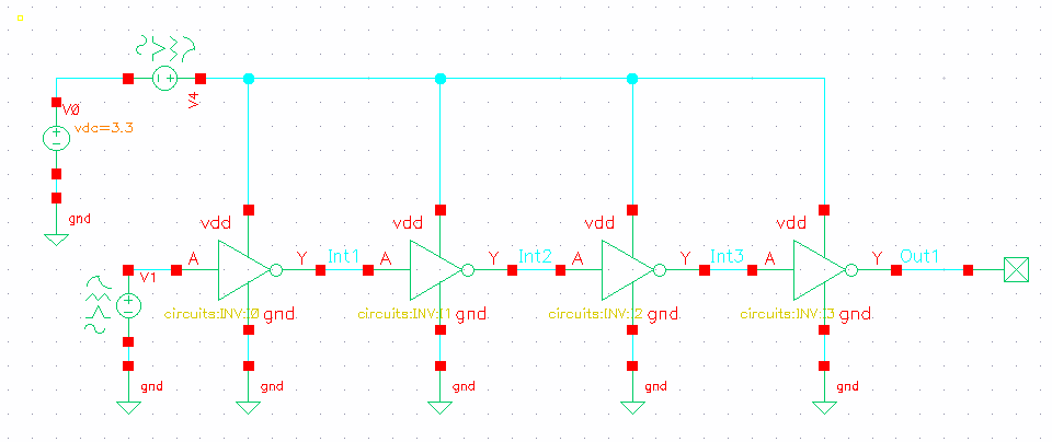
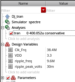

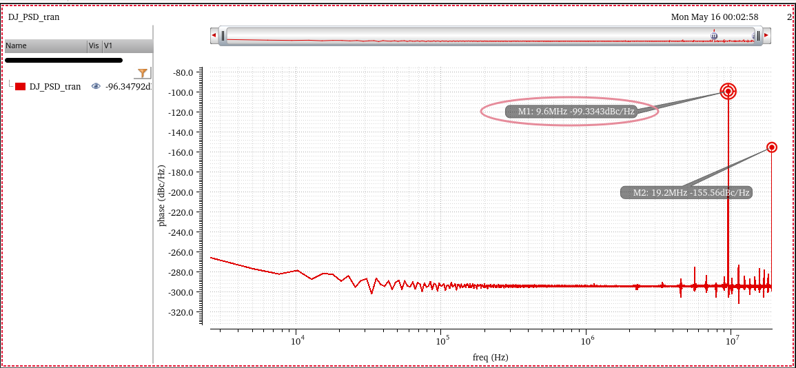
j_Djpp can be calculated by PSD,too
1 | fck = 38.4e6; |
1 | Jpp = |
For DJ, we usually use peak to peak value
BTW, the psd value at half of fundamental frequency (\(f_s/2\)) is
duty cycle distortion due to the NMOS/PMOS imbalance, because of rising only data
Random Jitter
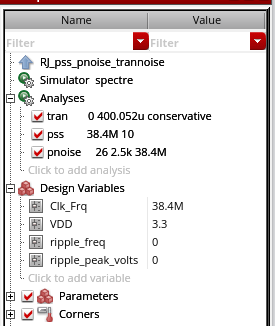
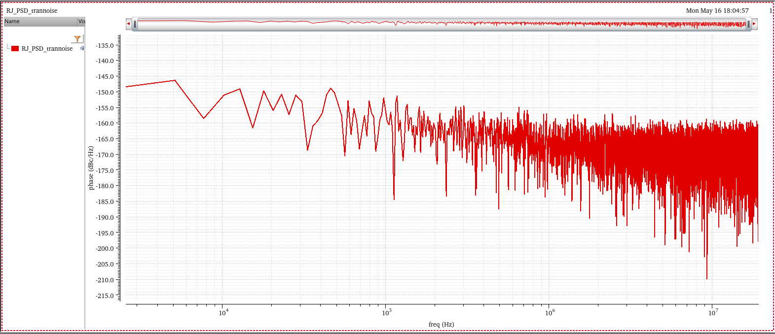
RJ can be accurately and efficiently measured using PSS/Pnoise or HB/HBnoise.
Note that the transient noise can also be used to compute RJ;
However, the computation cost is typically very high, and the accuracy is lesser as compared to PSS/Pnoise and HB/HBnoise.
Since RJ follows a Gaussian distribution, it can be fully characterized using its Root-Mean-Squared value (RMS) or the standard deviation value (\(\sigma\))
The Peak-to-Peak value of RJ (\(\text{RJ}_{\text{p-p}}\)) can be calculated under certain observation conditions \[ \text{RJ}_{\text{p-p}}\equiv K \ast \text{RJ}_{\text{RMS}} \] Here, \(K\) is a constant determined by the BER specification of the system given in the following Table
| BER | Crest factor (K) |
|---|---|
| \(10^{-3}\) | 6.18 |
| \(10^{-4}\) | 7.438 |
| \(10^{-5}\) | 8.53 |
| \(10^{-6}\) | 9.507 |
| \(10^{-7}\) | 10.399 |
| \(10^{-8}\) | 11.224 |
| \(10^{-9}\) | 11.996 |
| \(10^{-10}\) | 12.723 |
| \(10^{-11}\) | 13.412 |
| \(10^{-12}\) | 14.069 |
| \(10^{-13}\) | 14.698 |
1 | K = 14.698; |
1 | BER = |
Total Jitter
\[ \text{TJ}_{\text{p-p}}\equiv \text{DJ}_{\text{p-p}} + \text{RJ}_{\text{p-p}}(\text{BER}) \]

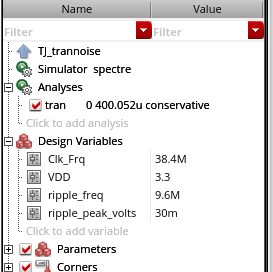
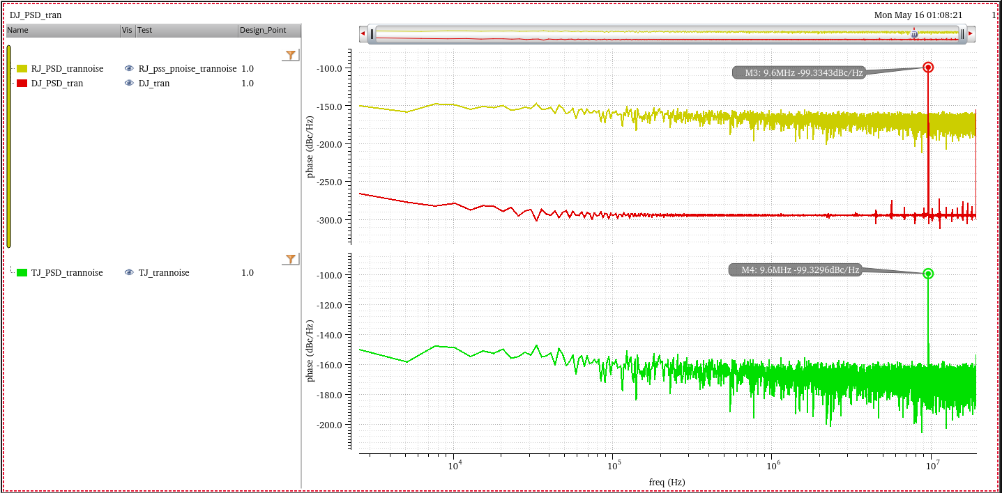
In the psd of TJ, the spur is DJ and floor is RJ
Phase Noise to Jitter
The phase noise is traditionally defined as the ratio of the power of the signal in 1Hz bandwidth at offset \(f\) from the carrier \(P\), divided by the power of the carrier \[ \ell (f) = \frac {S_v'(f_0+f)}{P} \] where \(S_v'\) is is one-sided voltage PSD and \(f \geqslant 0\)
Under narrow angle assumption \[ S_{\varphi}(f)= \frac {S_v'(f_0+f)}{P} \] where \(\forall f\in \left[-\infty +\infty\right]\)
Using the Wiener-Khinchin theorem, it is possible to easily derive the variance of the absolute jitter(\(J_{ee}\))via integration of the corresponding PSD \[ J_{ee,rms}^2 = \int S_{J_{ee}}(f)df \]
And we know the relationship between absolute jitter and excess phase is \[ J_{ee}=\frac {\varphi}{\omega_0} \] Considering that phase noise is normally symmetrical about the zero frequency, multiplied by two is shown as below \[ J_{ee,rms} = \frac{\sqrt{2\int_{0}^{+\infty}\ell(f)df}}{\omega_0} \] where phase noise is in linear units not in logarithmic ones.
Because the unit of phase noise in Spectre-RF is logarithmic unit (dBc), we have to convert the unit before applying the above equation \[ \ell[linear] = 10^{\frac {\ell [dBc/Hz]}{10}} \] The complete equation using the simulation result of Spectre-RF Pnoise is \[ J_{ee,rms} = \frac{\sqrt{2\int_{0}^{+\infty}10^{\frac {\ell [dBc/Hz]}{10}}df}}{\omega_0} \]
The above equation has been verified for sampled pnoise, i.e. Jee and Edge Phase Noise.
- For pnoise-sampled(jitter), Direct Plot Form - Function: Jee:Integration Limits can calculate it conveniently
- But for pnoise-timeaveage, you have to use the below equation to get RMS jitter.
One example, integrate to \(\frac{f_{osc}}{2}\) and \(f_{osc} = 16GHz\)

Of course, it apply to conventional pnoise simulation.
On the other hand, output rms voltage noise, \(V_{out,rms}\) divied by slope should be close to \(J_{ee,rms}\) \[ J_{ee,rms} = \frac {V_{out,rms}}{slope} \]
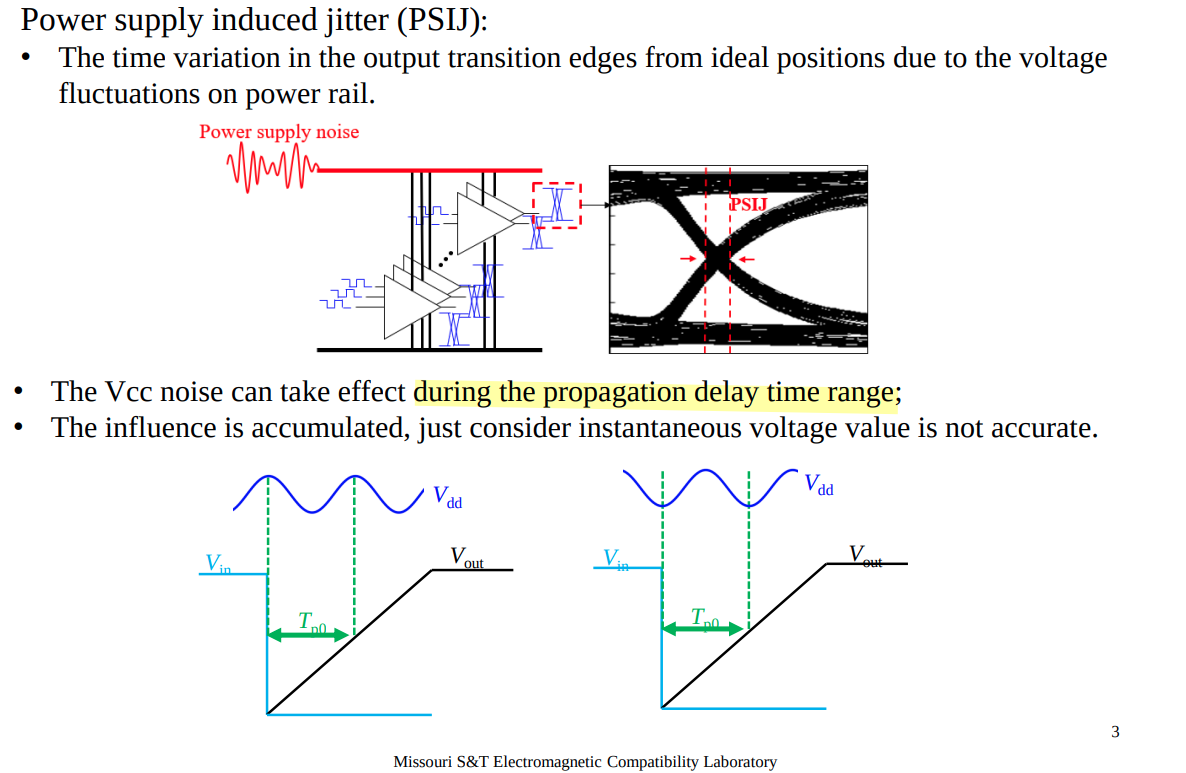
Power supply induced jitter (PSIJ)
Chulsoon Hwang. New Way to Improve Power Supply Induced Jitter Simulation Accuracy for IBIS Model [https://ibis.org/summits/aug21b/ding.pdf]
—, "A Generalized Power Supply Induced Jitter Model Based on Power Supply Rejection Ratio Response," in IEEE Transactions on Very Large Scale Integration (VLSI) Systems, vol. 29, no. 6, pp. 1052-1060, June 2021
—, DesignCon 2021. A Generalized Power Supply Induced Jitter Model Based on Power Supply Rejection Ratio Response [paper]
—, "Power Supply Induced Jitter: Introduction and Recent Advances," in IEEE Transactions on Signal and Power Integrity, vol. 5, pp. 22-32, 2026
X. Mo, J. Wu, N. Wary and T. C. Carusone, "Design Methodologies for Low-Jitter CMOS Clock Distribution," in IEEE Open Journal of the Solid-State Circuits Society, vol. 1, pp. 94-103, 2021. [https://ieeexplore.ieee.org/stamp/stamp.jsp?arnumber=9559395]
A sampled pxf analysis can be used to simulate the deterministic jitter of a circuit due to power supply ripple
TODO 📅
reference
Nicola Da Dalt, Intel. ISSCC 2017 Forum: High-Performance Clock Generation and Distribution in Very-High-Speed Wireline Transceivers
Mozhgan Mansuri. ISSCC2021 SC3: Clocking, Clock Distribution, and Clock Management in Wireline/Wireless Subsystems
Phillip Restle. ISSCC2021 SC4: Processor Clock Generation, Distribution, and Clock Sensor/Management Loops
Jihwan Kim,Intel, ISSCC 2023 Forum F1.5: Circuit Designs for 200+Gb/s Electrical Transceivers
J. Kim et al., "8.1 A 224Gb/s DAC-Based PAM-4 Transmitter with 8-Tap FFE in 10nm CMOS," 2021 IEEE International Solid-State Circuits Conference (ISSCC), San Francisco, CA, USA, 2021, pp. 126-128
Article (20500632) Title: How to simulate Random and Deterministic Jitters
Spectre Tech Tips: Measuring Noise in Digital Circuits - Analog/Custom Design - Cadence Blogs - Cadence Community [https://community.cadence.com/cadence_blogs_8/b/cic/posts/s . . .]
Cadence RAK: Deterministic Jitter Measurement using SpectreRF
Frank Wiedmann. Using sampled pxf analysis to simulate deterministic jitter [https://community.cadence.com/cadence_technology_forums/f/custom-ic-design/51605/using-sampled-pxf-analysis-to-simulate-deterministic-jitter]
supply noise sensitivity: PSS+PAC or PSS+PX [https://designers-guide.org/forum/YaBB.pl?num=1376500816]
J. Kim et al., "A 112 Gb/s PAM-4 56 Gb/s NRZ Reconfigurable Transmitter With Three-Tap FFE in 10-nm FinFET," in IEEE Journal of Solid-State Circuits, vol. 54, no. 1, pp. 29-42, Jan. 2019, [https://sci-hub.ru/10.1109/JSSC.2018.2874040]
— et al., "A 224-Gb/s DAC-Based PAM-4 Quarter-Rate Transmitter With 8-Tap FFE in 10-nm FinFET," in IEEE Journal of Solid-State Circuits, vol. 57, no. 1, pp. 6-20, Jan. 2022, [https://sci-hub.ru/10.1109/JSSC.2021.3108969]
J. N. Tripathi, V. K. Sharma and H. Shrimali, "A Review on Power Supply Induced Jitter," in IEEE Transactions on Components, Packaging and Manufacturing Technology, vol. 9, no. 3, pp. 511-524, March 2019 [https://sci-hub.st/10.1109/TCPMT.2018.2872608]
H. Kim, J. Fan and C. Hwang, "Modeling of power supply induced jitter (PSIJ) transfer function at inverter chains," 2017 IEEE International Symposium on Electromagnetic Compatibility & Signal/Power Integrity (EMCSI), Washington, DC, USA, 2017 [https://sci-hub.st/10.1109/ISEMC.2017.8077937]
High Speed Communications Part 8 – On Die CMOS Clock Distribution. [https://youtu.be/nx5CiHcwrF0]
Low-Jitter CMOS Clock Distribution [https://youtu.be/LMT-T41Y64U]
Sam Palermo. Spring 2025 ECEN720 : High-Speed Links Circuits and Systems [Lecture 14: Clock Distribution Techniques]
Muhammad Aldacher. Analog Design of Clock Distribution Network using Standing-Waves [https://github.com/muhammadaldacher/Analog-Design-of-Clock-Distribution-Network-using-Standing-Waves]
Rhee, W. (2020). Phase-locked frequency generation and clocking : architectures and circuits for modern wireless and wireline systems. The Institution of Engineering and Technology