ESD & Latchup
PERC
CD: current density checks
P2P: point to point resistance checks
LDL: logic driven layout checks, latch up related
TOPO: topology, circuit connection and device size checks
database
CD, P2P, LDL : dfmdb
TOPO: svdb
Frank Feng. New Approach For Full Chip Electrical Reliability Verification [pdf]
Calibre PERC Catalog Test-Cases & Common Examples Version 2.0
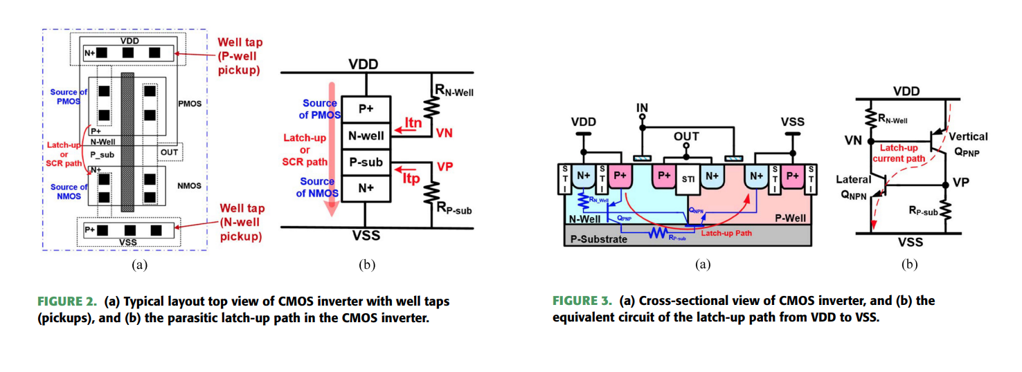
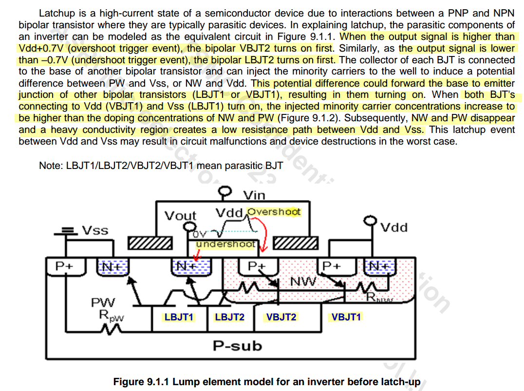
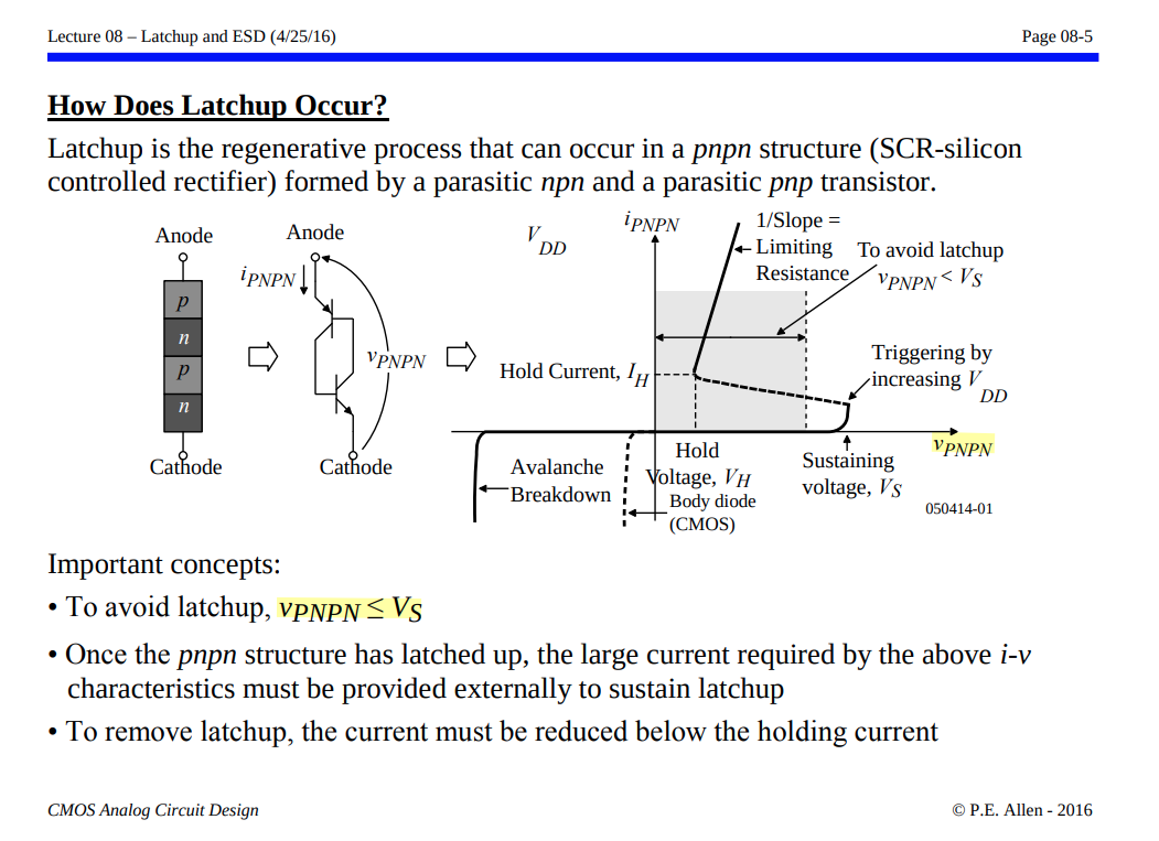
Latchup
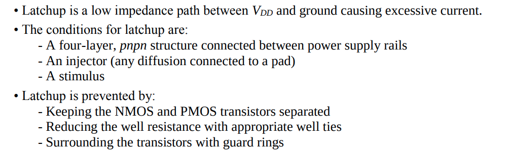
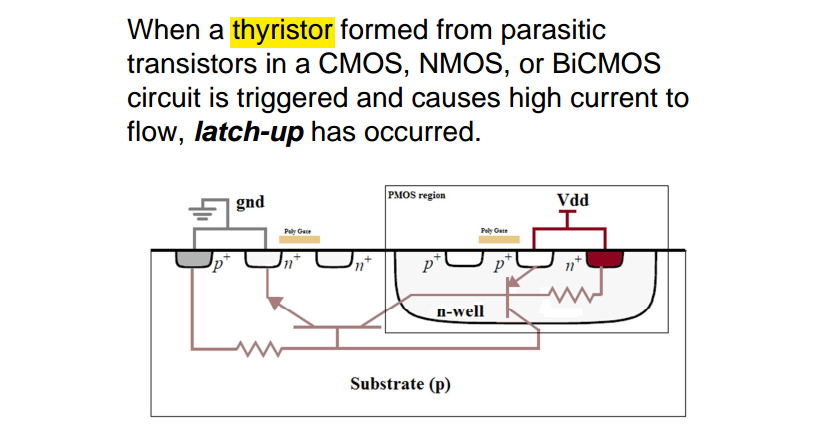
This can happen when a parasitic thyristor, which is essentially a pair of interconnected transistors, is triggered into a latched state, leading to sustained current flow and potential device failure.
latchup-prevention technique
Technical Paper Ensuring latch-up guard rings ESDA rules using Calibre PERC [https://resources.sw.siemens.com/en-US/technical-paper-ensuring-latch-up-guard-rings-esda-rules-using-calibre-perc/]
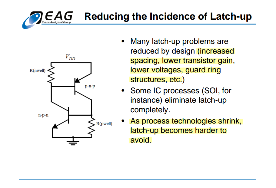
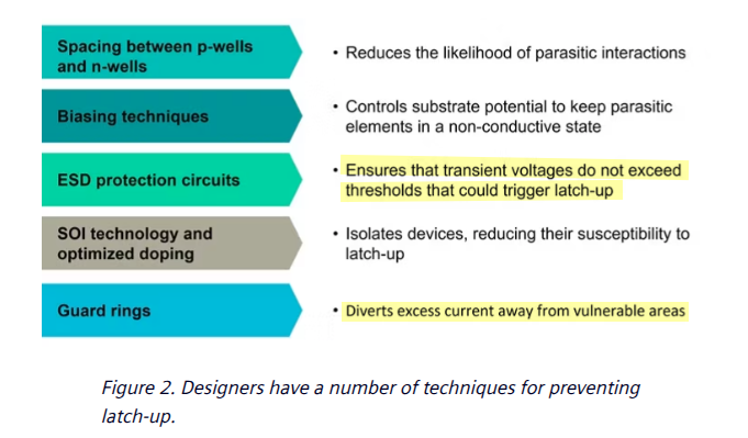
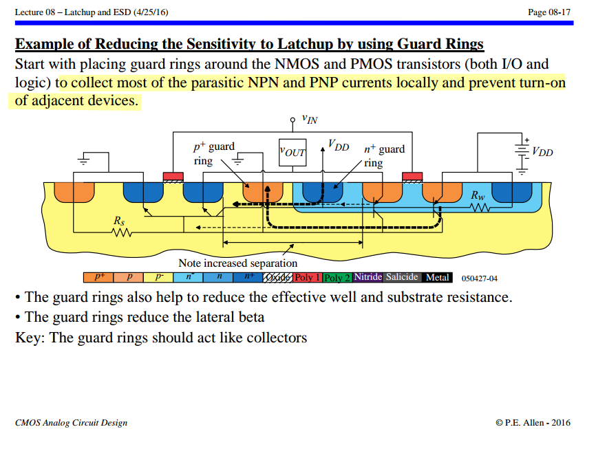
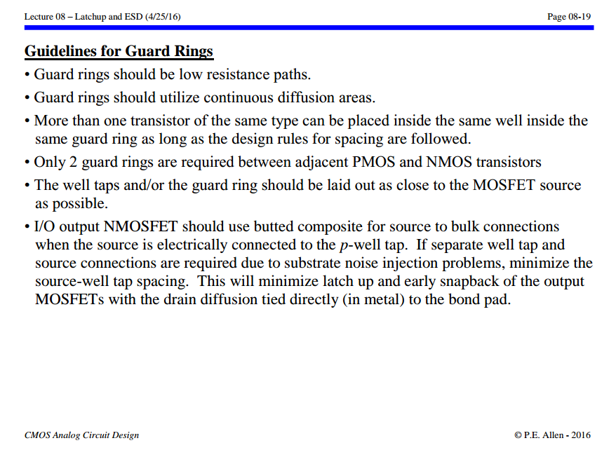
Guard Rings
One important technique is the use of guard rings, the heavily doped regions surrounding sensitive components on the IC to divert excess current away from vulnerable areas, thereby reducing the likelihood of latch-up occurrence
These guard rings not only function as barriers against parasitic thyristor formation but also serve to isolate different regions of the IC, minimizing unwanted electrical interactions and maintaining pathway integrity

P.E. Allen - 2016. CMOS Analog Circuit Design: Lecture 08 – Latchup and ESD (4/25/16) [https://aicdesign.org/wp-content/uploads/2018/08/lecture08-160425.pdf]
Transient-Induced Latchup
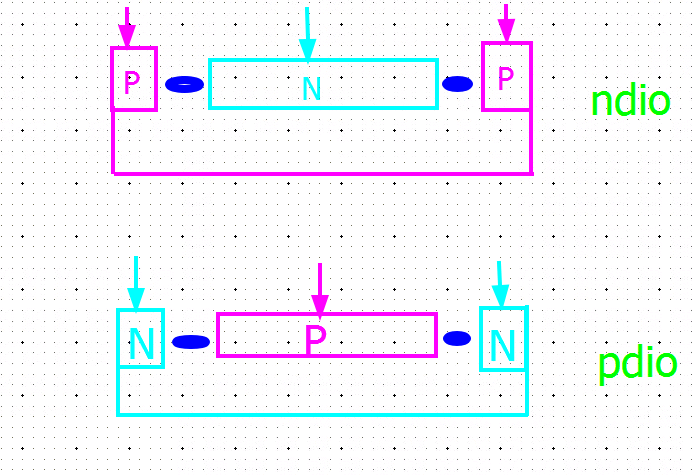
OD injector
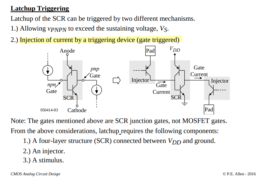
Silicon Controlled Rectifiers (SCR)
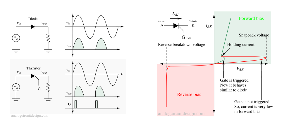
A thyristor (also known as a Silicon Controlled Rectifier or SCR) is a three-terminal semiconductor device used as an electronic switch or rectifier
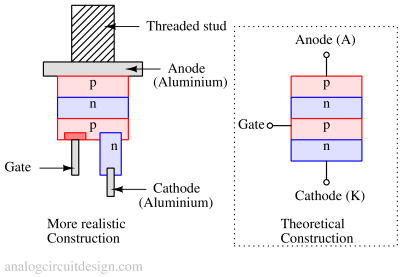
To turn the thyristor on, a positive voltage pulse is applied to the gate (G) terminal. This voltage pulse needs to be of sufficient magnitude to trigger the device. When the gate is triggered, it allows a small current to flow into the base of the P-N-P transistor within the thyristor structure
[https://ec2-44-207-46-173.compute-1.amazonaws.com/thyristor/]
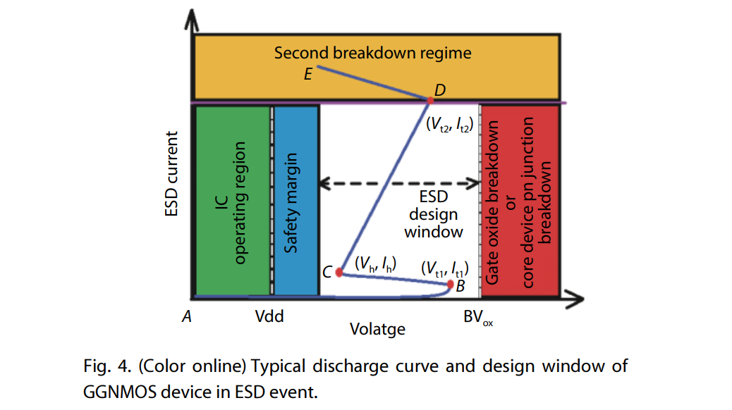
ESD design window
[https://monthly-pulse.com/2021/06/02/the-esd-design-window-concept/]
[https://www.researching.cn/ArticlePdf/m00098/2020/41/12/122403.pdf]
- Transparency
- Trigger voltage Vt1
- Holding/clamping voltage Vh
- Robustness
- failure current level It2
- Effectiveness
- maximum voltage of the clamp device: Vmax
Secondary protection
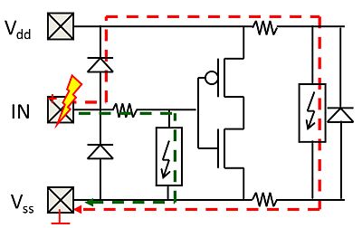
- Adding a (small) clamp behind the isolation resistance can extend the ESD design window, e.g. enabling dual diode protection for thin oxide transistors.
- ESD current through this clamp will build-up voltage across the isolation resistance, while protecting the circuit.
- The higher voltage at the IN pad will then trigger the primary protection (red current path)
Adding a (small) clamp behind the isolation resistance can extend the ESD design window, e.g. enabling dual diode protection for thin oxide transistors
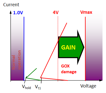
Extended ESD design window example. The failure voltage of a thin gate oxide in advanced CMOS is about 4V. The primary ESD solution (red IV curve) introduces too much voltage. Thanks to an isolation resistance between primary and secondary local clamp device (green IV curve) additional margin is created.
[https://monthly-pulse.com/2022/03/29/introduction-esd-protection-concepts-for-i-os/]
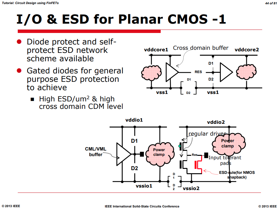
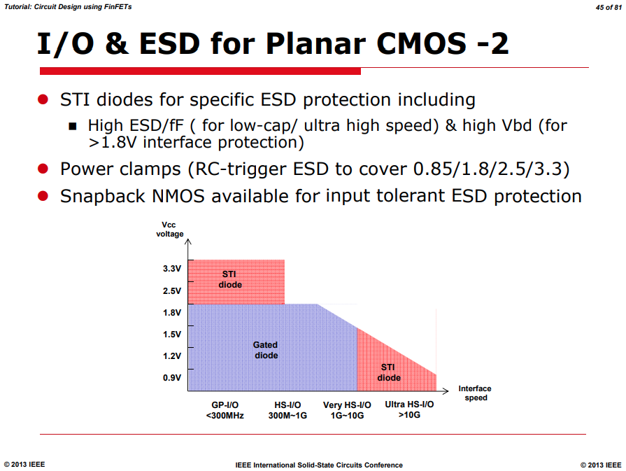
Gated diode & STI diode
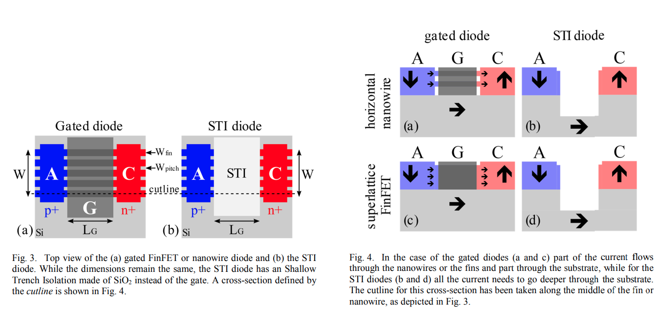
M. Simicic, G. Hellings, S. -H. Chen, N. Horiguchi and D. Linten, "ESD diodes with Si/SiGe superlattice I/O finFET architecture in a vertically stacked horizontal nanowire technology," 2018 48th European Solid-State Device Research Conference (ESSDERC), Dresden, Germany, 2018
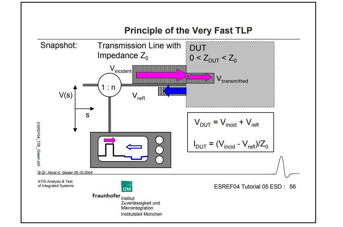
TLP/vf-TLP
TRANSMISSION LINE PULSE TESTING: THE INDISPENSABLE TOOL FOR ESD CHARACTERIZATION OF DEVICES, CIRCUITS AND SYSTEMS [https://www.esda.org/assets/News/1708-ESD-firstDraft.pdf]
[https://monthly-pulse.com/2021/06/08/transmission-line-pulse-tlp-test-system/]
Jon Barth "TLP and VFTLP Testing of Integrated Circuit ESD Protection" [https://barthelectronics.com/wp-content/uploads/2016/09/TLP-and-VFTLP-Test-of-Integrated-Circuit-ESD-Protection.pdf]
Horst A. Gieser(IZM), "ESD- Testing: HBM to very fast TLP" [https://www.thierry-lequeu.fr/data/ESREF/2004/Tut5.pdf]
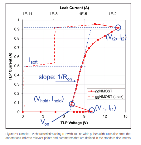
Vt1: trigger voltage
Vhold: holding voltage
soft failure current: Isoft
hard failure current: It2
TLP vs ESD
- ESD tests simulate real world events (HBM, MM, CDM)
- TLP does not simulate any real-world event
- ESD tests record failure level (Qualification)
- TLP tests record failure level and device behavior (Characterization)
TLP is not a qualification test, but a characterization method, which describes the resistance of a device for a given stimulus, aka. Device Characterization
Unlike ESD waveforms, TLP does not mimic any real world event
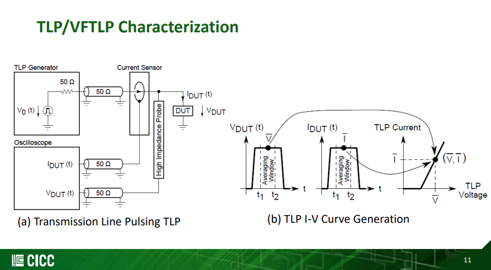
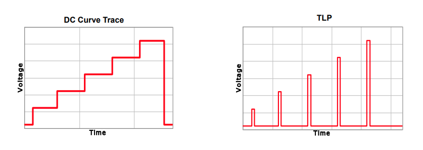
TLP and Curve Tracing
- Curve Tracing is DC; TLP is a short pulse
- Shorter pulse - Reduced duty cycle, less heating, which means higher voltage before failure
- Controlled Impedance - Allows device behavior to be observed
- Both measure resistance of device with increasing voltage
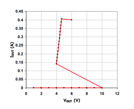
Device Characterization with TLP
- Turn-on time
- Snapback voltage
- Performance changes with rise time
VF-TLP and CDM differences
Question:
How well will VF-TLP results predict CDM testing performance?
Answer:
VF-TLP can be a guide to CDM failure levels, and provide a lot of understanding of a circuit's operation during CDM stressing, but simple correlations between VF-TLP failure current level and CDM withstand voltage levels are difficult to establish.
I.V and Leakage Evolution Plots
DC leakage current data combined with the I-V data provides electrical indications of where damage begins, and how rapidly it can evolve from soft to hard failures
Henry, Leo & Barth, Jon & Richner, John & Verhaege, Koen. (2000). Transmission Line Pulse Testing of the ESD Protection Structures in ICs - A Failure Analyst's Perspective. 203-213. 10.31399/asm.cp.istfa2000p0203. [https://barthelectronics.com/pdf_files/2000%20ISTFA%20TLP%20Testing%20of%20the%20ESD%20Protection%20Structure.pdf]
Henry, L.G. & Barth, Jon & Verhaege, K. & Richner, J.. (2001). Transmission-line pulse ESD testing of ICs: A new beginning. Compliance Engineering. 18. 46+53. [https://barthelectronics.com/pdf_files/CE%20TLP%20Article%20March-April%202001.pdf]
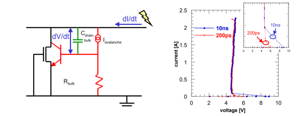
Snapback
Unfortunately, this protection concept is not effective anymore in
advanced FinFET technology. Our analysis showed that both core and IO
transistors are damaged at the onset of snapback in several FinFET
processes. 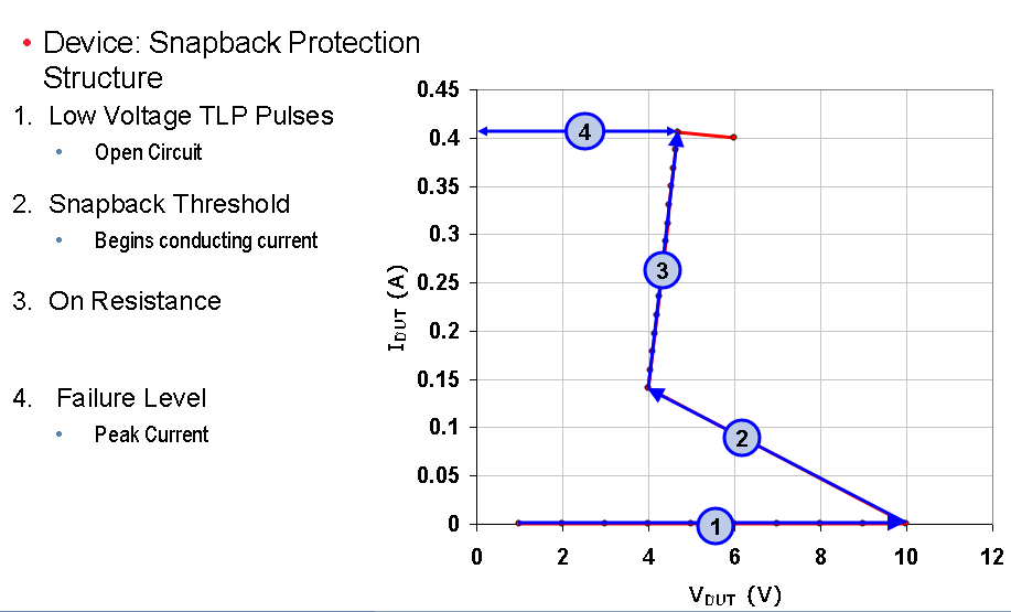
Lesson 2 - ESD Clamps [https://aicdesign.org/wp-content/uploads/2021/05/Lesson02_ESD_Clamps210315.pdf]
Introduction of Transmission Line Pulse (TLP) Testing for ESD Analysis - Device Level [https://www.esdemc.com/public/docs/TechnicalSlides/ESDEMC_TS001.pdf]
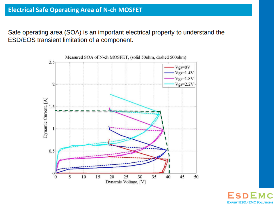
Safe operating area (SOA)
power clamp
Thanks to the device scaling the area is actually reasonable.
However, the leakage becomes the main bottleneck. 
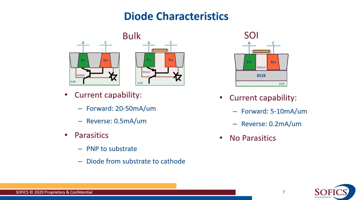
high current diode
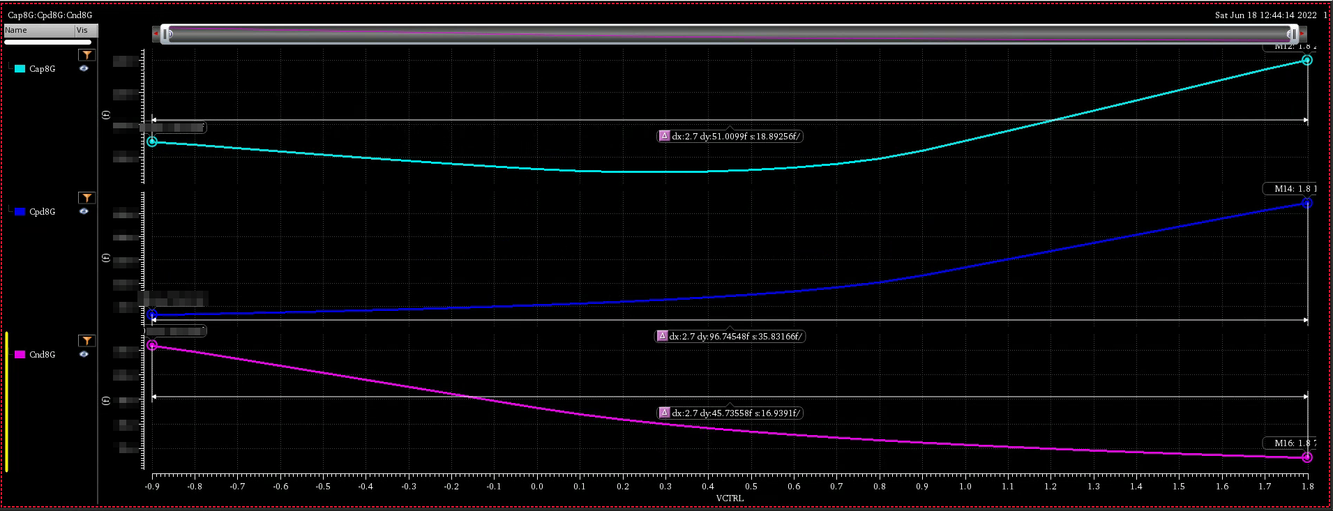
both diode are reverse-biased in normal operation, the PN Junction capacitance is proportional to forward-bias voltage
| Device | |
|---|---|
| ndio_mac | N+/P-well Diode |
| pdio_mac | P+/N-well Diode |
| ndio_18_mac | 1.8V N+/P-well Diode |
| pdio_18_mac | 1.8V P+/N-well Diode |
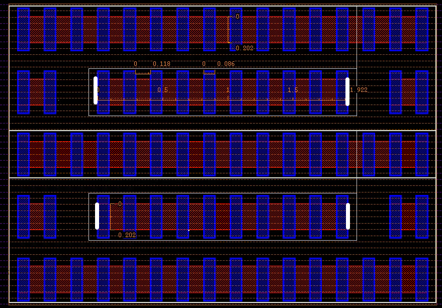
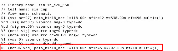
| ndio_hia18_mac | N-HIA Diode |
| pdio_hia18_mac | P-HIA Diode |
| ndio_gated18_mac | Thick Oxide N-Gated Diode |
| pdio_gated18_mac | Thick Oxide P-Gated Diode |
HIA_DIO can be used for logic or high speed circuits ESD protection
HIA: high current application purpose (High Amp)
There is no process difference between HIA_DIO and regular diode
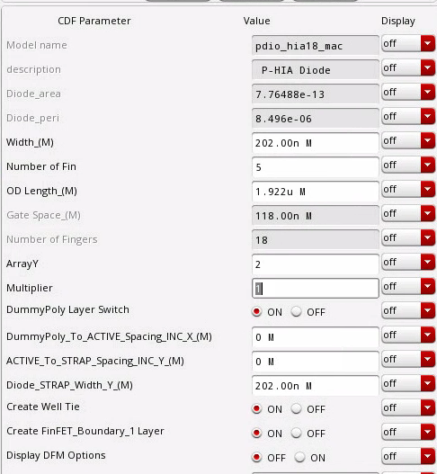
| width (W) | 2.020E-07 |
|---|---|
| Length (L) | 1.922E-06 |
| ArrayY (Ny) | 2 |
| Perimeter (Ny*2*(W+L)) | 8.496E-06 |
| Area (Ny*W*L) | 7.76488E-13 |
diode is drain/source originated, which is different from MOS (Gate originated)
The perimeter of diode in DRC is different from that in PERC deck, where PERC excludes the the left and right edge of OD
g after the rule numbers: DFM recommendations and guidelines
U: the rule is not checked by the DRC
MOS
lin netlist has different definition for MOS and diode.MOS: length of channel
diode: Gate space
HIA = High Amp
lateral diode: perimeter is key DRC rule for ESD diode
HIA diode process is same with regular junction diode
Dual Stacked Diodes
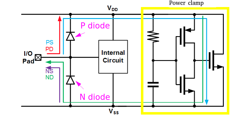
PS: I/O to GND positively
NS: I/O to GND negatively
PD: I/O to VDD positively
ND: I/O to VDD negatively
Dual diode should be used with power clamp for PS and ND path
PMOS power clamp

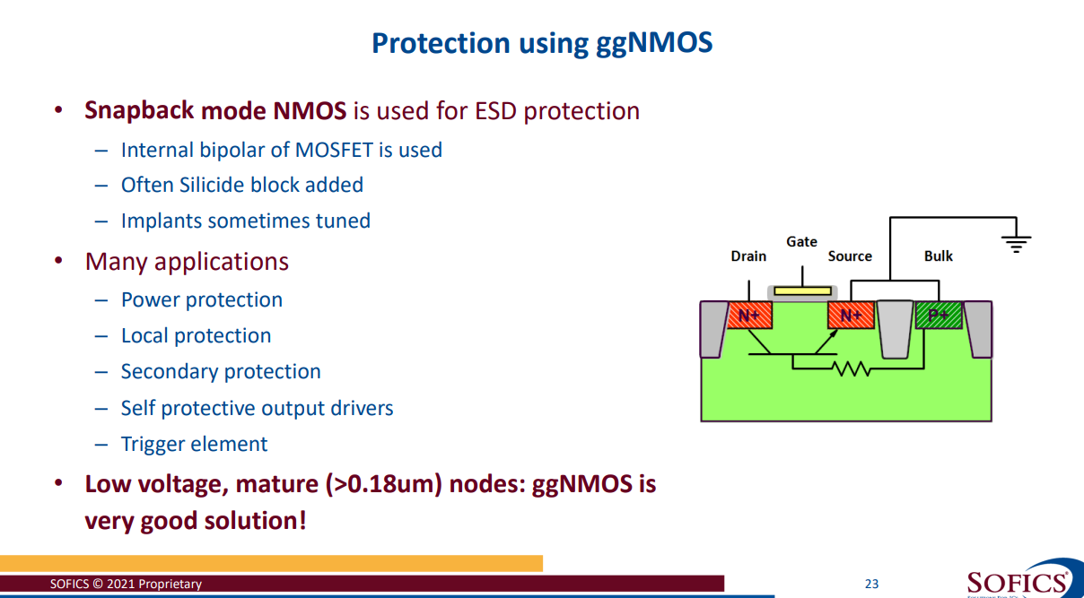
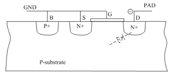
Gate grounded N-MOS (ggNMOS)
[https://monthly-pulse.com/2022/02/02/time-to-say-farewell-to-the-snapback-ggnmos-for-esd-protection/]
[https://monthly-pulse.com/2023/01/26/ggnmos-grounded-gated-nmos/]
Influence of the pulse rise time on ggNMOS. (left side) A fast ESD pulse can couple the bulk of the NMOS to a higher potential for a short period, reducing the trigger voltage. (right side) A clear Vt1 reduction is visible, while the remaining part of the IV curve remains the same.
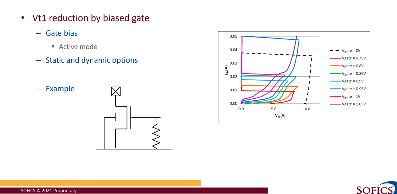
resistance between gate and source that designers typically use to reduce the Vt1 trigger voltage of a ggNMOS ESD protection
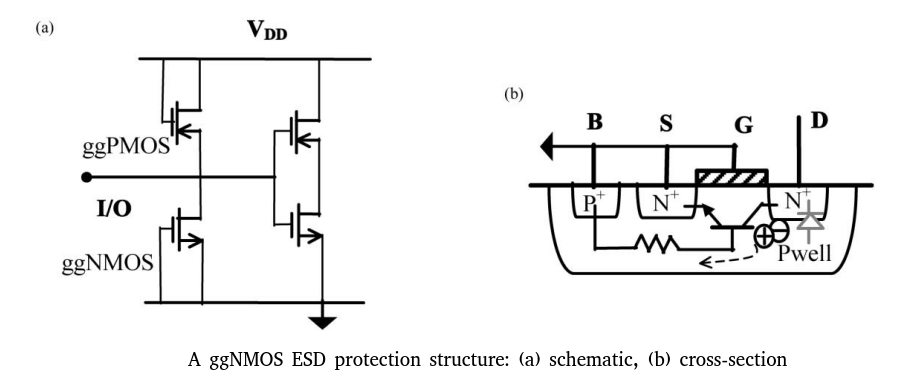
The drain (D) is connected to an I/O pad and the gate (G) is grounded.
To ensure “zero” leakage of the ESD protection structure under normal operations.
To to protect gate of core device, tie-high and tie-low shall be used when used as secondary ESD protection.
Positive ESD transient at I/O pad
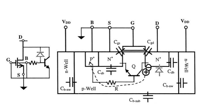
- DB junction is reverse-biased all the way to its breakdown.
- Avalance multiplication takes place and generates electron-hole pairs
- Hole current flows into the ground via the B-region and build up a potential, VR, across the lateral parasitic resistance R
- As VR increases, the BS junction turns on, eventually triggers the parasitic lateral NPN transistor Q (DBS)
Negative ESD transient at I/O pad
The forward-biased parasitic diode, BD, will shunt the transient
ggNMOS is commonly used in the GPIO provided by foundry, which alleviate the ESD design burden of customer.
These GPIO is self-protective thanks to the ggNMOS.
Reference
Introduction to Transmission Line Pulse (TLP), URL: https://tools.thermofisher.com/content/sfs/brochures/TLP%20Presentation%20May%202009.pdf
VF-TLP and CDM differences, URL: https://www.grundtech.com/app-note-vf-tlp-cdm-differences
ESD-Testing: HBM to very fast TLP URL: https://www.thierry-lequeu.fr/data/ESREF/2004/Tut5.pdf
S. Kim et al., "Technology Scaling of ESD Devices in State of the Art FinFET Technologies," 2020 IEEE Custom Integrated Circuits Conference (CICC), 2020, pp. 1-6, doi: 10.1109/CICC48029.2020.9075899.
KOEN DECOCK IEEE-SSCSLEUVEN "ON-CHIP ESD PROTECTION: BASIC CONCEPTS AND ADVANCED APPLICATIONS" [https://monthly-pulse.com/wp-content/uploads/2021/11/2021-11-sofics_presentation_ieee_final.pdf]
Yuanzhong Zhou, D. Connerney, R. Carroll and T. Luk, "Modeling MOS snapback for circuit-level ESD simulation using BSIM3 and VBIC models," Sixth international symposium on quality electronic design (isqed'05), 2005, pp. 476-481, doi: 10.1109/ISQED.2005.81.
Charged Device Model (CDM) Qualification Issues - Expanded [https://www.jedec.org/sites/default/files/IndustryCouncil_CDM_October2021_JEDECversion_September2022_rev1.pdf]
Wang, Albert ZH. On-chip ESD protection for integrated circuits: an IC design perspective. Vol. 663. Springer Science & Business Media, 2002.
Wang, Albert. Practical ESD Protection Design. John Wiley & Sons, 2021.
Ker, Ming-Dou, and Sheng-Fu Hsu. Transient-induced latchup in CMOS integrated circuits. John Wiley & Sons, 2009. [https://picture.iczhiku.com/resource/eetop/wyiGjQaHOgrYFcxB.pdf]
Milin Zhang, "Low Power Circuit Design Using Advanced CMOS Technology" River Publishers 2018
Barry Fernelius, Evans Analytical Group. Latch-up Testing [https://site.ieee.org/ocs-cpmt/files/2013/06/Latch-up_at_EAG_IEEE_September_2013.pdf]
M. -D. Ker and Z. -H. Jiang, "Overview on Latch-Up Prevention in CMOS Integrated Circuits by Circuit Solutions," in IEEE Journal of the Electron Devices Society, vol. 11, pp. 141-152, 2023 [https://ieeexplore.ieee.org/stamp/stamp.jsp?arnumber=9998049]