Dual Diode and ggNMOS
HIA diode
HIA = High Amp
lateral diode: perimeter is key DRC rule for ESD diode
HIA diode process is same with regular junction diode
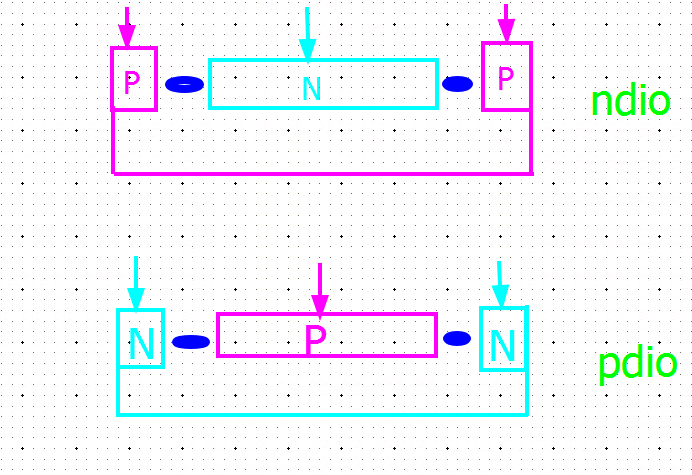
Dual Stacked Diodes
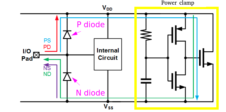
PS: I/O to GND positively
NS: I/O to GND negatively
PD: I/O to VDD positively
ND: I/O to VDD negatively
Dual diode should be used with power clamp for PS and ND path
PMOS power clamp

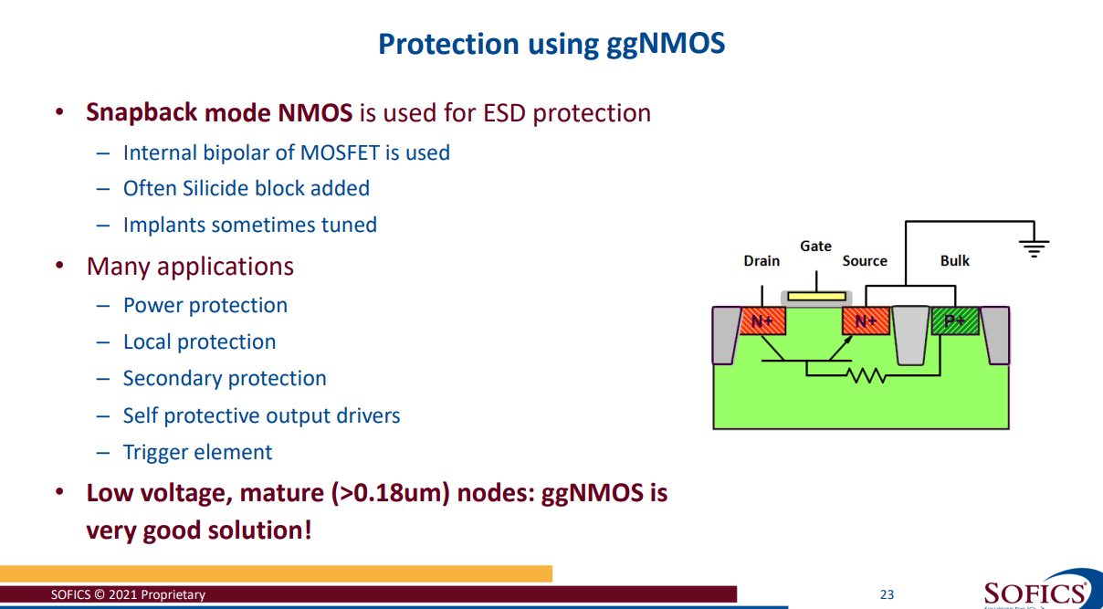
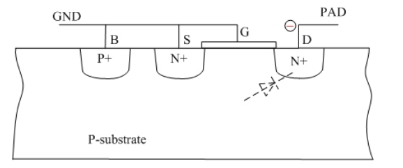
ggNMOS (grounded-gate NMOS)
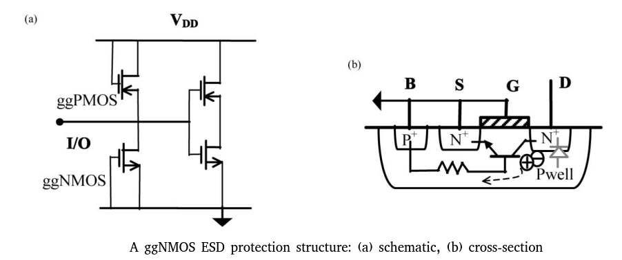
The drain (D) is connected to an I/O pad and the gate (G) is grounded.
To ensure “zero” leakage of the ESD protection structure under normal operations.
To to protect gate of core device, tie-high and tie-low shall be used when used as secondary ESD protection.
[https://monthly-pulse.com/wp-content/uploads/2021/11/2021-11-sofics_presentation_ieee_final.pdf]
Positive ESD transient at I/O pad
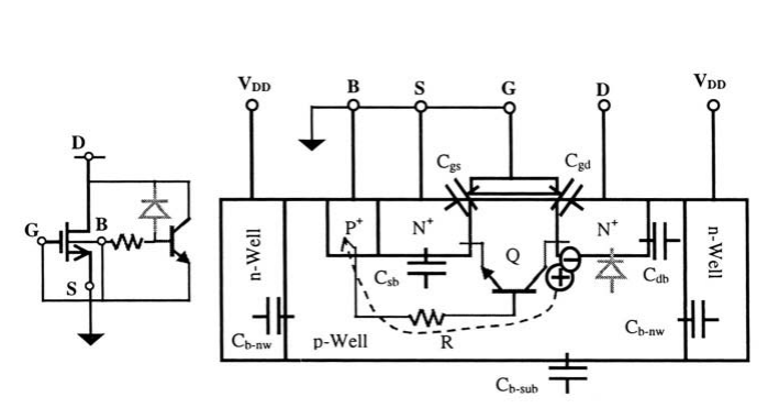
- DB junction is reverse-biased all the way to its breakdown.
- Avalance multiplication takes place and generates electron-hole pairs
- Hole current flows into the ground via the *B-region** and build up a potential, VR, across the lateral parasitic resistance R
- As VR increases, the BS junction turns on, eventually triggers the parasitic lateral NPN transistor Q (DBS)
Negative ESD transient at I/O pad
The forward-biased parasitic diode, BD, will shunt the transient
ggNMOS is commonly used in the GPIO provided by foundry, which alleviate the ESD design burden of customer.
These GPIO is self-protective thanks to the ggNMOS.
reference
Wang, Albert Z. H. 2002. On-chip ESD protection for integrated circuits: an IC design perspective. Boston, Mass: Kluwer Academic Publishers.
Wang, Anq i & Feng, H.G & Gong, K & Zhan, Ruqing & Stine, J. (2001). On-chip ESD protection design for integrated circuits: An overview for IC designers. Microelectronics Journal. 32. 733-747. 10.1016/S0026-2692(01)00060-X.
Feng, Haigang, Ke Gong, Rouying Zhan and Albert Z. Wang. “On-Chip ESD Protection Design for Ics.” (2001).
Introduction: ESD protection concepts for I/Os. URL: https://monthly-pulse.com/2022/03/29/introduction-esd-protection-concepts-for-i-os/
Answer: What does "strap" mean in this context? https://electronics.stackexchange.com/a/591759?stw=2
Hammer VLSI Flow URL: https://fires.im/micro22-slides-pdf/04_hammer_vlsi.pdf
Calibre Rule Writing 2009