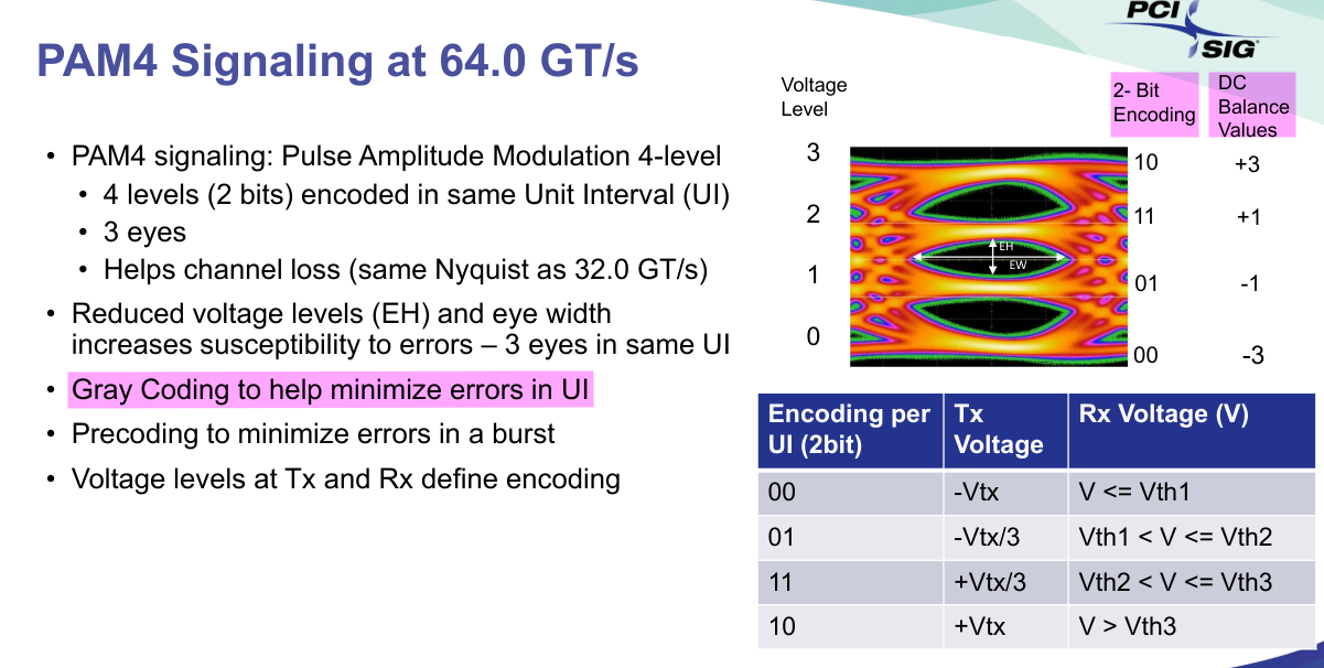
PAM4 Signaling
Why PAM4?
Bandwidth
[How Interconnects Work: Bandwidth for Modeling and Measurements, https://www.simberian.com/AppNotes/HIW-Bandwidth-6to112-2021-11-08.pdf]
[Moving from 28 Gbps NRZ to 56 Gbps PAM-4 - is it "free lunch"?, https://www.simberian.com/AppNotes/28NRZto56PAM4.pdf]
[PAM4: For Better and Worse Is PAM4 worth the hassle?https://www.signalintegrityjournal.com/articles/1151-pam4-for-better-and-worse]
PAM4 Basic
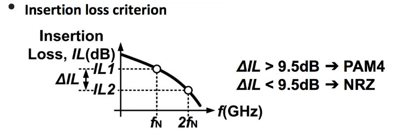
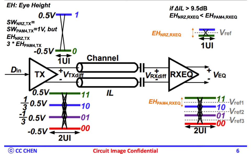
PAM4 only have 1/3 of the amplitude compared to NRZ \[ \text{SNR loss} = 20\log(\frac{1}{3}) \sim 9.5\text{dB} \]
In practice, there is further degradation due to nonlinearity
In a more technical terms, we trade the transmitter's signal-to-noise ratio (SNR) for lower Nyquist frequency
Equalization will be a lot more complex
Energy
1mW/Gbps = 1pJ/bit
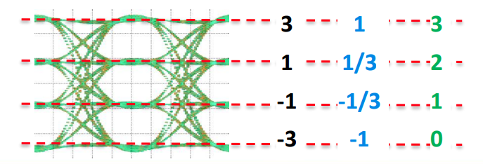
PAM4 Level Names
PAM4 Eye Linearity
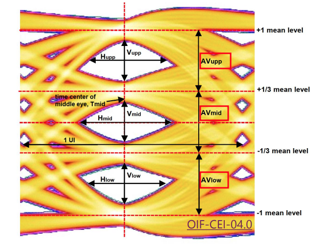
Each level can have different amplitudes, which form the Eye Linearity \[ {\text{Eye Linearity}}=\frac{\min(AV_{\text{upp}},AV_{\text{mid}},AV_{\text{low}})}{\max(AV_{\text{upp}},AV_{\text{mid}},AV_{\text{low}})} \]
Perfect eye = 1
Worst eye = 0
Transmitter Linearity (RLM)
The Level Separation Mismatch Ratio, commonly referred to as \(R_{\text{LM}}\), is a measurement that is not required in normative or informative VSR tests, but is required by most other variants.
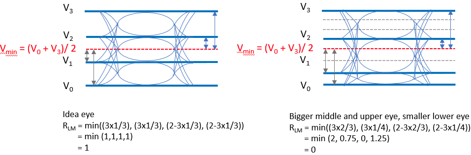
\[\begin{align} V_{\text{mid}} &= \frac{V_0+V_3}{2} \\ ES1 &= \frac{V_1-V_{\text{mid}}}{V_0-V_{\text{mid}}} \\ ES2 &= \frac{V_2-V_{\text{mid}}}{V_3-V_{\text{mid}}} \\ R_{\text{LM}} &= \min(3\times ES1, 3\times ES2, 2-3\times ES1, 2-3\times ES2) \end{align}\]
where ES means Effective Symbol Level
\(R_{\text{LM}}\) is conceptually similar to eye linearity but measured differently. An ideal PAM4 eye has \(R_{\text{LM}}\) equal to 1, but it does not scale in the same way as eye linearity.
The closer \(R_{\text{LM}}\) is to 1, the better the eye linearity is.
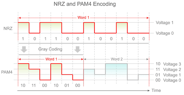
Gray Coding
Gray code or reflected binary code was designed so that two successive values differ by one bit
Reducing the number of switching
| Linear Code | Gray Code |
|---|---|
| 11 | 10 |
| 10 | 11 |
| 01 | 01 |
| 00 | 00 |
- Only one bit error per symbol is made for incorrect decisions
- This is the coding adopted in all the PAM4 standards
- Support dual-mode with PAM2, by grounding the LSB
- MSB is the bit transmitted first
Binary to PAM4 and Back to Binary Example
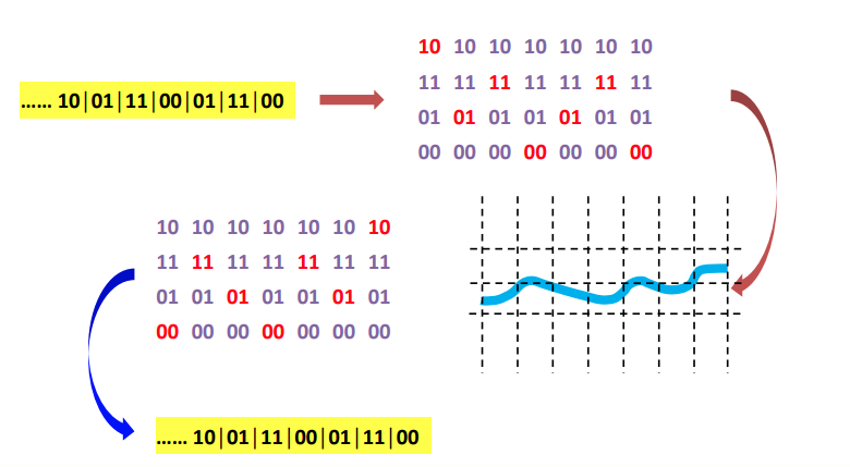
The way that Gray coding combines the MSB (most significant bit) and LSB (least significant bit) in each PAM4 symbol assures that symbol errors caused by amplitude noise are more likely to cause one bit error than two. On the other hand, jitter is more likely to cause two bit errors per symbol error.
PAM4 TX equalization
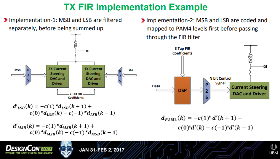
Here, \(d_{\text{LSB}} \in \{-1, 1\}\), \(d_{\text{MSB}} \in \{-2, 2\}\) and \(d' \in \{ -3, -1, 1, 3 \}\)
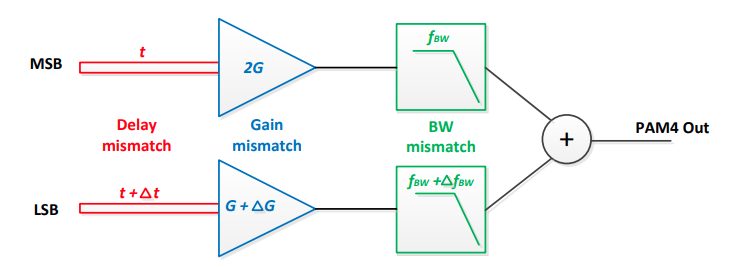
Implementation-1 could potentially experience performance degradation due to
- Clock skew, \(\Delta t\), could make the eye misaligned horizontally
- Gain mismatch, \(\Delta G\), could cause eye nonlinearity
- Bandwidth mismatch, \(\Delta f_{\text{BW}}\), could make the eye misaligned vertically
Typically, a 3-tap FIR (pre + main + post) TX de-emphasis is used
3-tap FIR results in \(4^3 = 64\) possible distinct signal levels

\[\begin{align} R_U^M \parallel R_D^M &= \frac{3R_T}{2}\\ R_U^L \parallel R_D^L &= 3R_T \end{align}\]
Thevenin Equivalent Circuit is 
Which can be simpified as  \[\begin{align}
V_{\text{rx}} &= \frac{1}{2}(V_p - V_m) \\
&= \frac{1}{2}(\frac{2}{3}(2V_{\text{MSB}}+V_{\text{LSB}})-1) \\
&=\frac{1}{3}(2V_{\text{MSB}}+V_{\text{LSB}})-\frac{1}{2}
\end{align}\]
\[\begin{align}
V_{\text{rx}} &= \frac{1}{2}(V_p - V_m) \\
&= \frac{1}{2}(\frac{2}{3}(2V_{\text{MSB}}+V_{\text{LSB}})-1) \\
&=\frac{1}{3}(2V_{\text{MSB}}+V_{\text{LSB}})-\frac{1}{2}
\end{align}\]
The above eqations demonstrate that the output \(V_{\text{rx}}\) is the linear sum of MSB and LSB; LSB and MSB have relative weight, i.e. 1 for LSB and 2 for MSB.
Assume pre cusor has \(L\) legs, main cursor \(M\) legs and post cursor \(N\) legs, which is same with the convention in "Voltage-Mode Driver Equalization"
The number of legs connected with supply can expressed as \[ n_{up} = (1-d_{n+1})L + d_{n}M + (1-d_{n-1})N \] Where \(d_n \in \{0, 1\}\), or \[ n_{up} = \frac{1}{2}(-D_{n+1}+1)L + \frac{1}{2}(D_{n}+1)M + \frac{1}{2}(-D_{n-1}+1)N \] Where \(D_n \in \{-1, +1\}\)
Then the number of legs connected with ground is \[ n_{dn}=L+M+N-n_{up} \] where \(n_{up}+n_{dn}=L+M+N\)
Voltage resistor divider \[\begin{align} V_o &= \frac{\frac{R_{U}}{n_{dn}}}{\frac{R_U}{n_{dn}}+\frac{R_U}{n_{up}}} \\ &= \frac{1}{2}- \frac{1}{2}D_{n+1}\frac{L}{L+M+N}+ \frac{1}{2}D_{n}\frac{M}{L+M+N}-\frac{1}{2}D_{n-1}\frac{N}{L+M+N} \\ &= \frac{1}{2}-\frac{1}{2}D_{n+1}\cdot l+ \frac{1}{2}D_{n}\cdot m-\frac{1}{2}D_{n-1}\cdot n \end{align}\]
where \(l+m+n=1\)
\(V_{\text{MSB}}\) and \(V_{\text{LSB}}\) can be obtained
\[\begin{align} V_{\text{MSB}} &= \frac{1}{2}-\frac{1}{2}D^{\text{MSB}}_{n+1}\cdot l+ \frac{1}{2}D^{\text{MSB}}_{n}\cdot m-\frac{1}{2}D^{\text{MSB}}_{n-1}\cdot n \\ V_{\text{LSB}} &= \frac{1}{2}-\frac{1}{2}D^{\text{LSB}}_{n+1}\cdot l+ \frac{1}{2}D^{\text{LSB}}_{n}\cdot m-\frac{1}{2}D^{\text{LSB}}_{n-1}\cdot n \end{align}\]
Substitute the above equation into \(V_{\text{rx}}\), we obtain the relationship between driver legs and FFE coefficients
\[\begin{align} V_{\text{rx}} &=\frac{1}{3}(2V_{\text{MSB}}+V_{\text{LSB}})-\frac{1}{2} \\ &= \frac{1}{3} \left\{ 2\left( \frac{1}{2}-\frac{1}{2}D^{\text{MSB}}_{n+1}\cdot l+ \frac{1}{2}D^{\text{MSB}}_{n}\cdot m- \frac{1}{2}D^{\text{MSB}}_{n-1}\cdot n \right) + \left( \frac{1}{2}-\frac{1}{2}D^{\text{LSB}}_{n+1}\cdot l+ \frac{1}{2}D^{\text{LSB}}_{n}\cdot m- \frac{1}{2}D^{\text{LSB}}_{n-1}\cdot n \right) \right\}-\frac{1}{2} \\ &= \left(-\frac{l}{6} \cdot 2 \cdot D^{\text{MSB}}_{n+1}+ \frac{m}{6} \cdot 2 \cdot D^{\text{MSB}}_{n}- \frac{n}{6} \cdot 2 \cdot D^{\text{MSB}}_{n-1}\right) + \left(-\frac{l}{6} \cdot D^{\text{LSB}}_{n+1}+ \frac{m}{6} \cdot D^{\text{LSB}}_{n}- \frac{n}{6} \cdot D^{\text{LSB}}_{n-1}\right) \\ &= -\frac{l}{6}(2 \cdot D^{\text{MSB}}_{n+1}+D^{\text{LSB}}_{n+1})+ \frac{m}{6}(2\cdot D^{\text{MSB}}_{n}+D^{\text{LSB}}_{n}) -\frac{n}{6}(2\cdot D^{\text{MSB}}_{n-1}+D^{\text{LSB}}_{n-1}) \end{align}\]
After scaling, we obtain \[ V_{\text{rx}} = -l\cdot(2 \cdot D^{\text{MSB}}_{n+1}+D^{\text{LSB}}_{n+1})+ m\cdot(2\cdot D^{\text{MSB}}_{n}+D^{\text{LSB}}_{n}) - n \cdot(2\cdot D^{\text{MSB}}_{n-1}+D^{\text{LSB}}_{n-1}) \] Where \(C_{-1} = l\), \(C_0 = m\) and \(C_{1}=n\), which is same with that of NRZ.
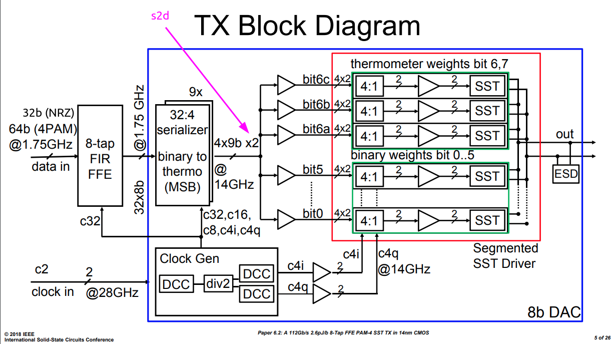
TX Serializer
mux timing

divider latch timing

Two latches

DAC-based FFE in PAM4 Transmitter
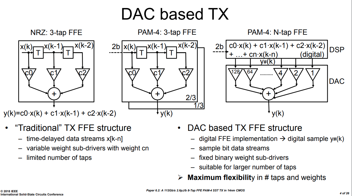
One classic TX implementation contain:
- a DAC: 56GS/s 8b
- a DSP: 8-tap FIR
C. Menolfi et al., "A 112Gb/S 2.6pJ/b 8-Tap FFE PAM-4 SST TX in 14nm CMOS," 2018 IEEE International Solid - State Circuits Conference - (ISSCC), 2018, pp. 104-106, doi: 10.1109/ISSCC.2018.8310205.
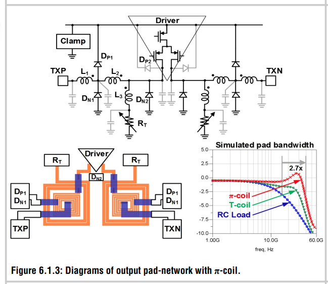
\(\pi\)-coil
J. Kim et al., "A 112Gb/s PAM-4 transmitter with 3-Tap FFE in 10nm CMOS," 2018 IEEE International Solid - State Circuits Conference - (ISSCC), 2018, pp. 102-104, doi: 10.1109/ISSCC.2018.8310204.
reference
C. Menolfi et al., "A 112Gb/S 2.6pJ/b 8-Tap FFE PAM-4 SST TX in 14nm CMOS," 2018 IEEE International Solid - State Circuits Conference - (ISSCC), 2018, pp. 104-106, doi: 10.1109/ISSCC.2018.8310205.
E. Chong et al., "A 112Gb/s PAM-4, 168Gb/s PAM-8 7bit DAC-Based Transmitter in 7nm FinFET," ESSCIRC 2021 - IEEE 47th European Solid State Circuits Conference (ESSCIRC), 2021, pp. 523-526, doi: 10.1109/ESSCIRC53450.2021.9567801.
B. Razavi, "Design Techniques for High-Speed Wireline Transmitters," in IEEE Open Journal of the Solid-State Circuits Society, vol. 1, pp. 53-66, 2021, doi: 10.1109/OJSSCS.2021.3112398.
Wang, Z., Choi, M., Lee, K., Park, K., Liu, Z., Biswas, A., Han, J., Du, S., & Alon, E. (2022). An Output Bandwidth Optimized 200-Gb/s PAM-4 100-Gb/s NRZ Transmitter With 5-Tap FFE in 28-nm CMOS. IEEE Journal of Solid-State Circuits, 57(1), 21-31. https://doi.org/10.1109/JSSC.2021.3109562
J. Kim et al., "A 112Gb/s PAM-4 transmitter with 3-Tap FFE in 10nm CMOS," 2018 IEEE International Solid - State Circuits Conference - (ISSCC), 2018, pp. 102-104, doi: 10.1109/ISSCC.2018.8310204.
PCIe® 6.0 Specification: The Interconnect for I/O Needs of the Future PCI-SIG® Educational Webinar Series, [https://pcisig.com/sites/default/files/files/PCIe%206.0%20Webinar_Final_.pdf]