temperature sensor
Due to the fact that long-term drift of temperature sensors and bandgap references caused by package-induced stress is lower with PNP BJTs than with NPN BJTs, PNP BJTs have been used traditionally for temperature sensor design in CMOS
Calibration
TODO 📅
\(V_{BE}\) curvature
curvature results in results in non-linearity
Though it is assumed that \(V_{BE}\) is a linear function of temperature for first oder analysis.
In practice, \(V_{BE}\) is slightly nonlinear, the magnitude of this nonlinearity is referred to as curvature.
curvature depends on the temperature dependency of the saturation current (\(I_s\)), and on that of the collector current (\(I_c\)), it can be written as \[ V_{curv}(T)=\frac{k}{q}(\eta-\delta)(T-T_r-T\cdot \ln(\frac{T}{T_r})) \] where \(\eta\) = a constant depending on the doping level, CMOS substrate pnp transistors have a typically value of \(\eta \cong 4\)
\(\delta\) = order of the temperature dependence of collector current (\(I_c\))
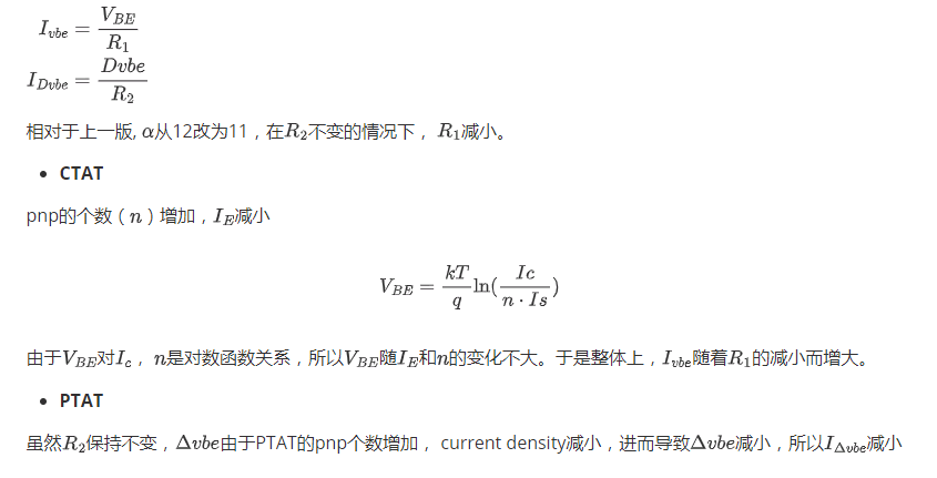
PTAT \(I_c\) help reduce \(V_{curv}(T)\), \(\delta=1\)
Although the temperature dependence of the bias current \(I_b\) doesn’t impact the accuracy of \(V_{BE}\), it does impact the systematic nonlinearity or curvature of \(V_{BE}\), and hence the sensor's systematic error. The curvature in \(V_{BE}\) can be reduced by using a PTAT bias current.
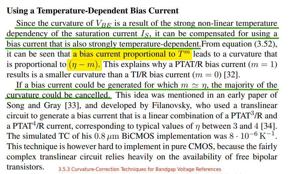
PTAT bias current
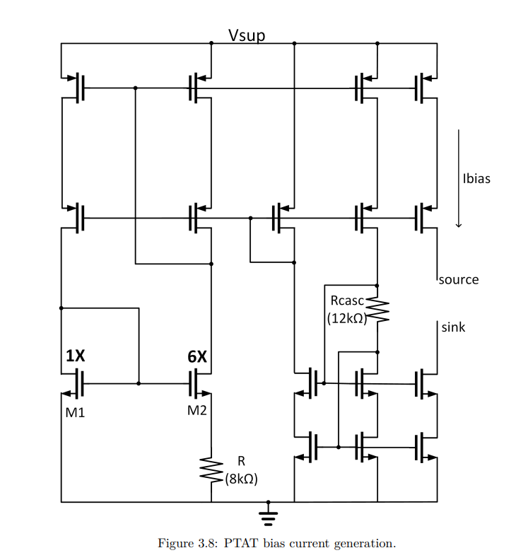 \[
I_{bias} = \frac{0.7}{\beta \cdot R^2}
\] in which \(\beta=\frac{\mu_{n}\cdot
C_{ox}\cdot W}{L}\), where:
\[
I_{bias} = \frac{0.7}{\beta \cdot R^2}
\] in which \(\beta=\frac{\mu_{n}\cdot
C_{ox}\cdot W}{L}\), where:
\(\mu_n\)=mobility,
\(C_{ox}\) = oxide capacitance density,
\(\frac{W}{L}\) = dimension ratio of unit NMOS used for \(M_1\) and \(M_2\)
\(\mu_n\) is complementary to the absolute temperature and resitor R is implemented using high-R flow in FinFET which has a low temperature dependency, the net temperature dependency of \(I_{bias}\) is proportional to the absolute temperature \[ I_{bias}\propto T \]
Kamath, Umanath Ramachandra. "BJT Based Precision Voltage Reference in FinFET Technology." (2021).
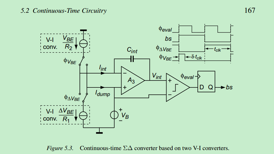
Errors due to V-I Finite Gain
Finite gain introduces errors both in the V-I converters, finite loop gain results in errors in the closed-loop transconductances.
 \[\begin{align}
(V_{i1} - V_{o1})\cdot A_{OL1} &= V_{o1} \\
V_{o1} &= \frac{A_{OL1}}{1+A_{OL1}}V_{i1} \\
I_{o1} &= \frac{A_{OL1}}{1+A_{OL1}}\frac{1}{R_1}V_{i1}
\end{align}\] similarly, \[
I_{o2} = \frac{A_{OL2}}{1+A_{OL2}}\frac{1}{R_2}V_{i2}
\]
\[\begin{align}
(V_{i1} - V_{o1})\cdot A_{OL1} &= V_{o1} \\
V_{o1} &= \frac{A_{OL1}}{1+A_{OL1}}V_{i1} \\
I_{o1} &= \frac{A_{OL1}}{1+A_{OL1}}\frac{1}{R_1}V_{i1}
\end{align}\] similarly, \[
I_{o2} = \frac{A_{OL2}}{1+A_{OL2}}\frac{1}{R_2}V_{i2}
\]
Then, \(\alpha\) is obtained \[ \alpha = \frac{(1+A_{OL2})A_{OL1}}{A_{OL2}(1+A_{OL1})}\cdot\frac{R_2}{R_1} \] Since the loop gains in the two V-I converters cannot be expected to match, the resulting errors in both converters should be reduced to negligible levels.
First, assume \(A_{OL2}=\infty\) \[\begin{align} \Delta \alpha &= (1-\frac{A_{OL1}}{1+A_{OL1}})\cdot\frac{R_2}{R_1}\\ &=\frac{1}{1+A_{OL1}}\cdot\frac{R_2}{R_1}\\ &\cong \frac{1}{A_{OL1}}\cdot\frac{R_2}{R_1} \end{align}\]
We get \[ \frac{\Delta \alpha}{\alpha}=\frac{1}{A_{OL1}} \] Follow the same procedure, assume \(A_{OL1}=\infty\) \[ \frac{\Delta \alpha}{\alpha}=\frac{1}{A_{OL2}} \] The finite gain introduces an error inversely proportional to the loop gain \(A_{OL1}\),\(A_{OL2}\), the resulting errors in both converters should be reduced to negligible levels
Why is it named as "bandgap reference"
Let us write the output voltage as \[ V_{REF} = V_{BE} + V_T\cdot \ln n \] and hence \[ \frac{\partial V_{REF}}{\partial T} = \frac{\partial V_{BE}}{\partial T} + \frac{V_T}{T}\ln n \] Setting this to zero and substituting for \(\frac{\partial V_{BE}}{\partial T}\), we have \[ \frac{V_{BE}-(4+m)V_T-E_g/q}{T}=-\frac{V_T}{T}\ln n \] If \(V_T\ln n\) is found from this equation and inserted in \(V_{REF}\), we obtain \[ V_{REF}=\frac{E_g}{q} + (4+m)V_T \]
The term bandgap is used here because as \(T\to 0\), \(V_{REF} \to E_g/q\)
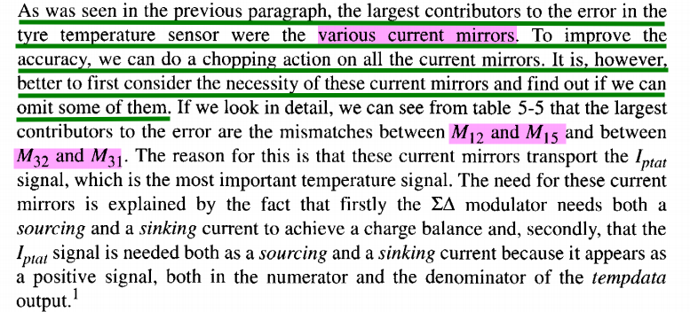
sinking PTAT-current generator without current mirrors
why without current mirror?
Bakker, Anton. (2000). High-Accuracy CMOS Smart Temperature Sensors. 10.1007/978-1-4757-3190-3. [https://repository.tudelft.nl/record/uuid:fd398056-48dd-4d84-8ae8-27a1b011d2c3]
Readout Circuit
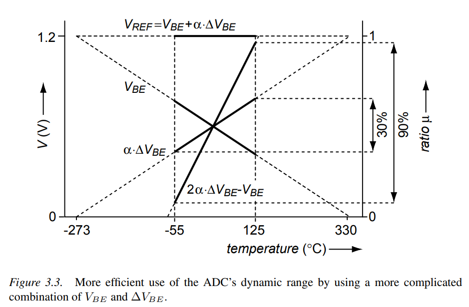
ADC dynamic range
Take \(V_{PTAT}=\alpha \cdot \Delta V_{BE}\) as input and \(V_{REF}\) as reference. The output \(\mu\) of the ADC will then be \[ \mu =\frac{V_{PTAT}}{V_{VREF}}=\frac{\alpha \cdot \Delta V_{BE}}{V_{BE}+\alpha \cdot \Delta V_{BE}} \] A final digital output \(D_{out}\) in degrees Celsius can be obtained by linear scaling: \[ D_{out}=A\cdot \mu + B \] where \(A\simeq 600K\) and \(B\simeq -273K\)
While the transfer is simple, it only uses about 30% of the of the ADC (the extremes of the operating range correspond to \(\mu \simeq 1/3\) and \(\mu \simeq 2/3\)). The ratio results in a rather inefficient use of the modulator's dynamic range.
For a first-order \(\Sigma\Delta\) modulator, this means that about 1.5 bits of resolution are lost
A more efficient transfer is \[ \mu '=\frac{2\alpha \cdot \Delta V_{BE}-V_{BE}}{V_{BE}+\alpha \cdot \Delta V_{BE}} \] With this more efficient combination, 90% of the dynamic range is used rather than 30%. Thus, the required resolution of the ADC is reduced by a factor of three.
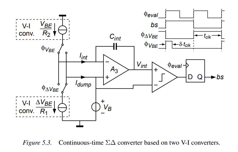
Integrator Output Swing
\[ \mu =\frac{\alpha \cdot \Delta V_{BE}}{V_{BE}+\alpha \cdot \Delta V_{BE}} \]
\[ \mu '=\frac{2\alpha \cdot \Delta V_{BE}-V_{BE}}{V_{BE}+\alpha \cdot \Delta V_{BE}} \]
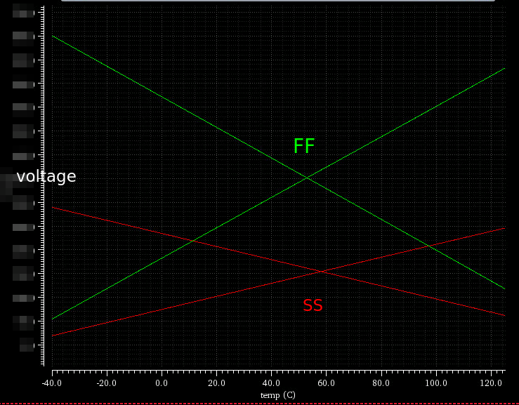
In advanced process, like Finfet 16nm, 7nm, high resistance resistor has +/-15% variation and MOM capacitor has +/-30% variation.
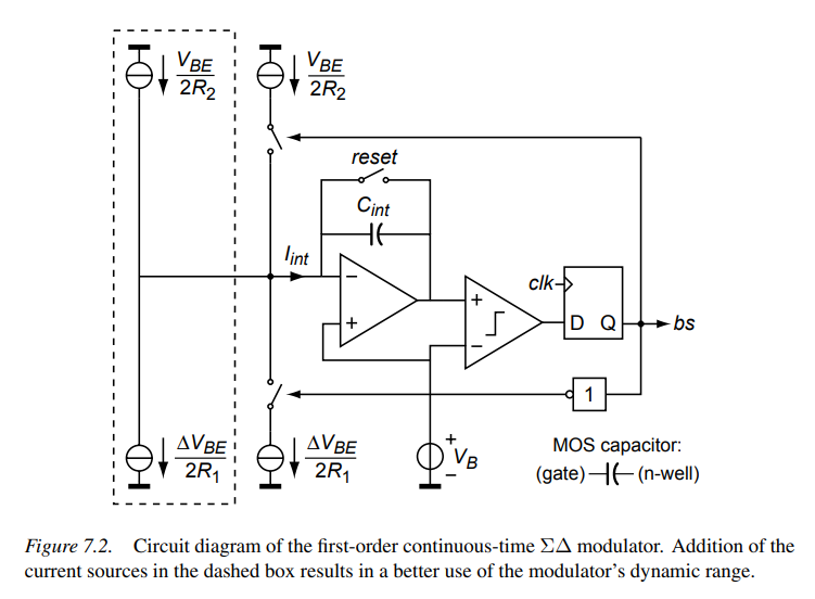
Then, \(R_1\) and \(R_2\) not only determine the \(\alpha\) but also the integrator's output swing, so do \(V_{BE}\) and \(\Delta V_{BE}\), \(C_{int}\).
The integrator's output change per period
example
integrator, comparator offset
integrator offset
comparator offset
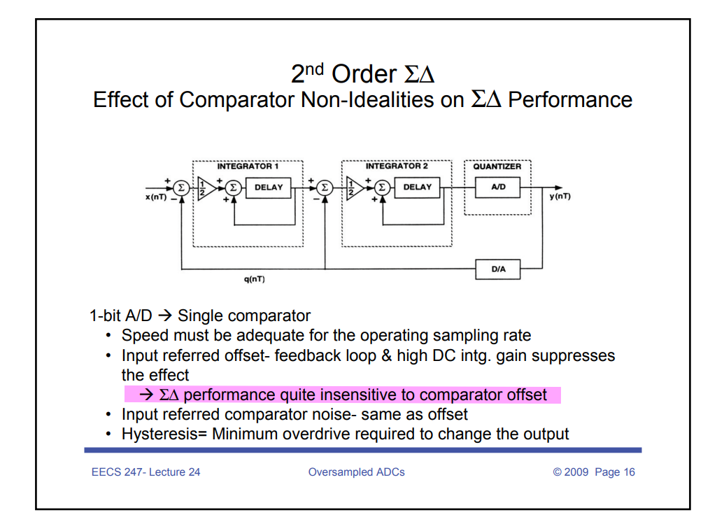
integrator design
application in sensor
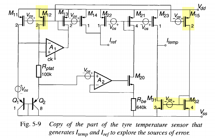
Offset Errors
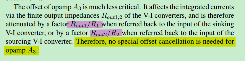
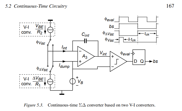
The offset of opamp \(A_3\) is much less critical:
It affects the integrated currents via the finite output impedances \(R_{out1,2}\) of the V-I converters, and is therefore attenuated by a factor \(R_{out1}/R_1\) when referred back to the input of the sinking V-I converter,
or by a factor \(R_{out2}/R_2\) when referred back to the input of the sourcing V-I converter.
Therefore, no special offset cancellation is needed for opamp \(A_3\).
The current change due to offset of \(A_3\): \[\begin{align} \frac{V_{BE,os}}{R_1} &= \frac{V_{ota,os}}{R_{out1}} \\ \frac{\Delta V_{BE,os}}{R_2} &= \frac{V_{ota,os}}{R_{out2}} \end{align}\] Then, the input referenced offset is: \[\begin{align} V_{BE,os} &=\frac{ V_{ota,os}}{R_{out1}/R_1} \\ \Delta V_{BE,os} &= \frac{ V_{ota,os}}{R_{out2}/R_2} \end{align}\]
Errors due to Finite Gain
Finite gain of opamp \(A_3\) results in a non-zero overdrive voltage at its input, which modulates the current Iint due to the finite output impedances of the V-I converters.
Assuming the opamp is implemented as a transconductance amplifier, there are two main causes of this non-zero overdrive voltage
- The finite transconductance \(g_{m3}\) of the opamp, , which implies that an overdrive voltage is required to provide the feedback current
The change in the integrated current
\[\begin{align} \Delta I_{int} &= \frac{V_{i,ota}}{R_{out}}\\ &= \frac{I_{int}}{g_{m3}}\cdot \frac{1}{R_{out}} \end{align}\]
- The finite DC gain \(A_{0,3}\), which implies that an overdrive voltage is required to produce the output voltage \(V_{int}\)
reference
Micheal, A., P., Pertijs., Johan, H., Huijsing., Pertijs., Johan, H., Huijsing. (2006). Precision Temperature Sensors in CMOS Technology.
C. -H. Chang, J. -J. Horng, A. Kundu, C. -C. Chang and Y. -C. Peng, "An ultra-compact, untrimmed CMOS bandgap reference with 3σ inaccuracy of +0.64% in 16nm FinFET," 2014 IEEE Asian Solid-State Circuits Conference (A-SSCC), 2014, pp. 165-168, doi: 10.1109/ASSCC.2014.7008886.
EE247 - Analog Digital Interface Integrated Circuits - Fall 2009 Lecture 24- Oversampled ADCs
Hecht, Bruce. (2010). SSCS DL Kofi Makinwa Talks About Smart Sensor Design at SSCS-Boston [People]. Solid-State Circuits Magazine, IEEE. 2. 54 - 56. 10.1109/MSSC.2009.935278.