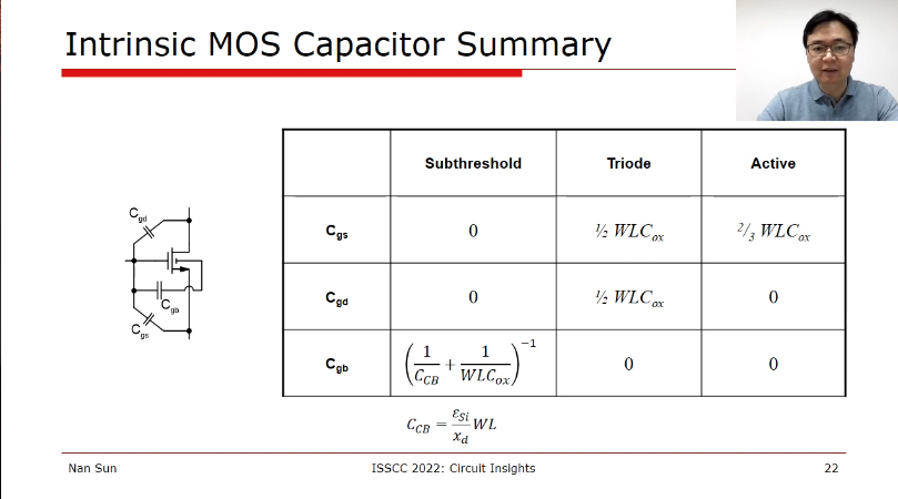
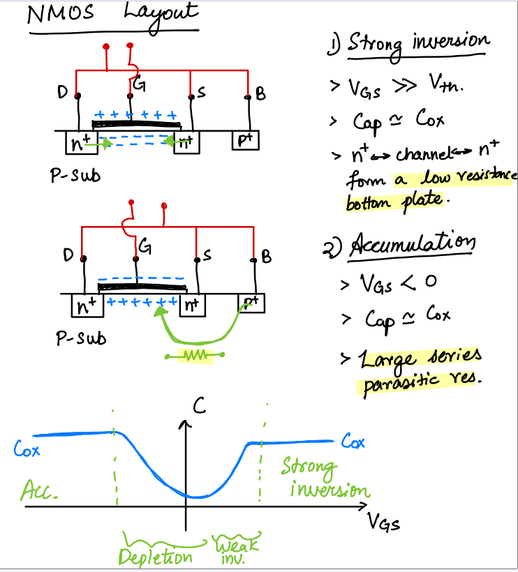
MOS Capacitor
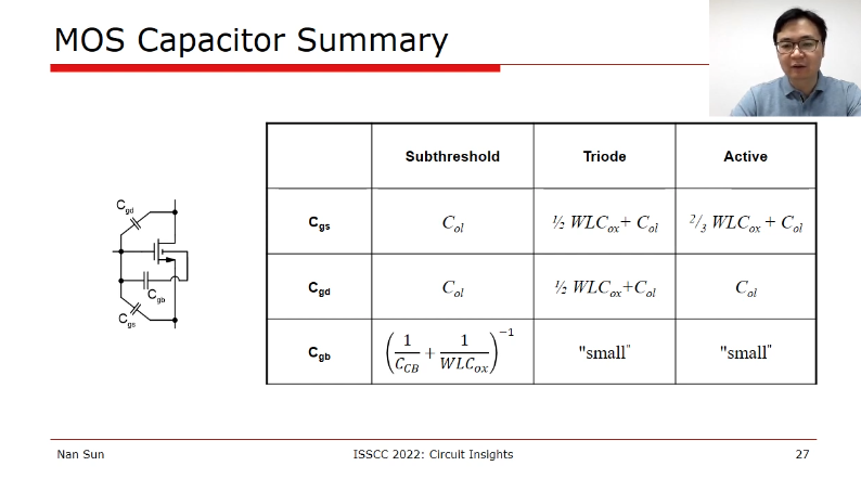
MOS capacitances
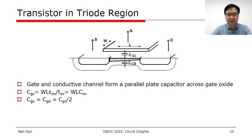
- oxide capacitance (aka gate-channel
capacitance) between the gate and the channel
\(C_1=WLC_{ox}\)
- divided between \(C_{GS}\) and \(C_{GD}\)
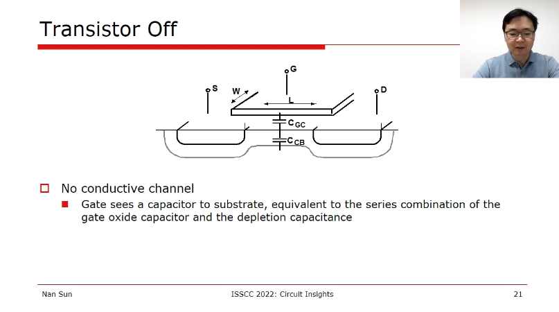
- depletion capacitance between the channel and the substrate \(C_2\)
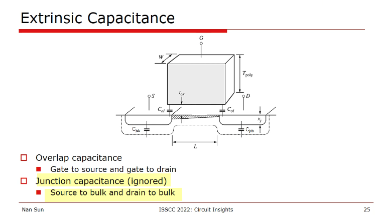
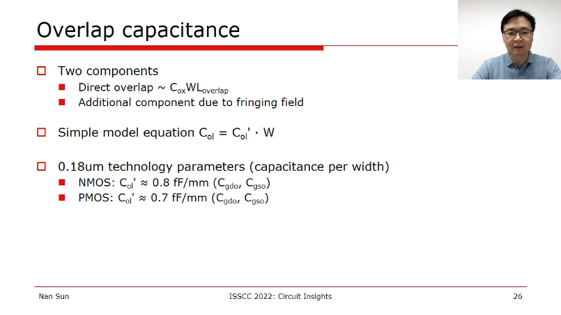
- overlap capacitance: direct overlap and fringing field
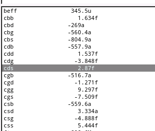
- junction capacitance between the
source/drain areas and the substrate
- The value of \(C_{SB}\) and \(C_{DB}\) is a function of the source and drain voltages with respect to the substrate
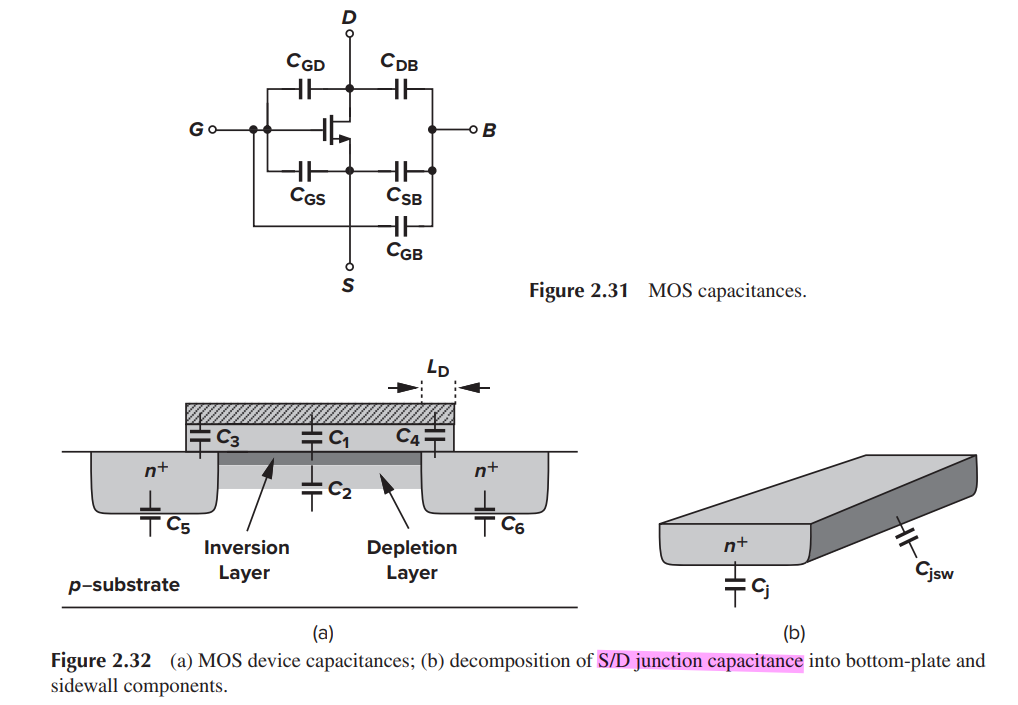
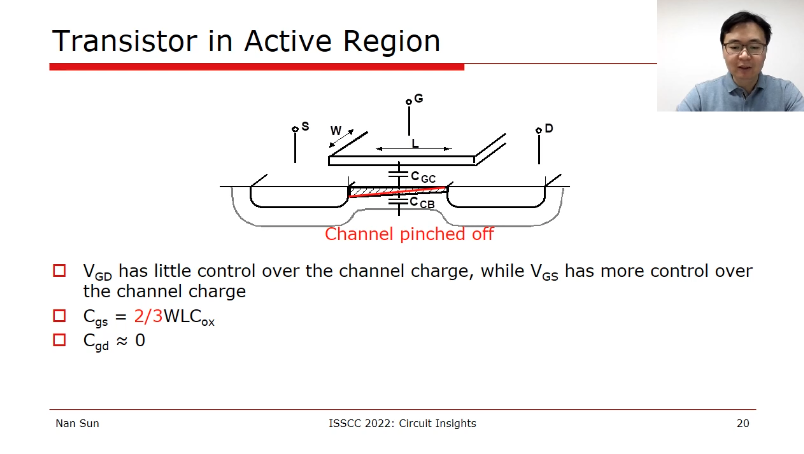
The gate-bulk capacitance is usually neglected in the triode and saturation regions because the inversion layer acts as a "shield" between the gate and the bulk.
classification with Intrinsic and Extrinsic MOS capacitor
[Circuit Insights - 11-CI: Fundamentals 4 Tsinghua Nan Sun]
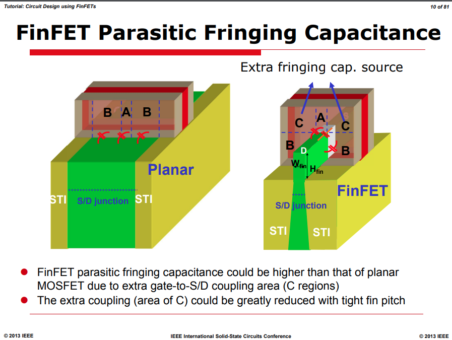
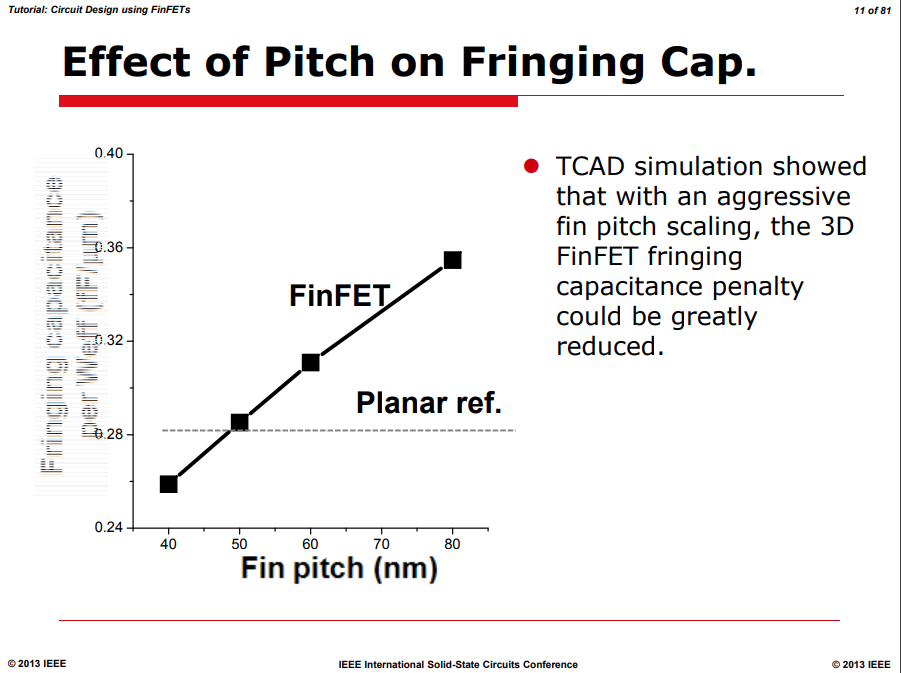
FinFET Parasitic Fringing Capacitance
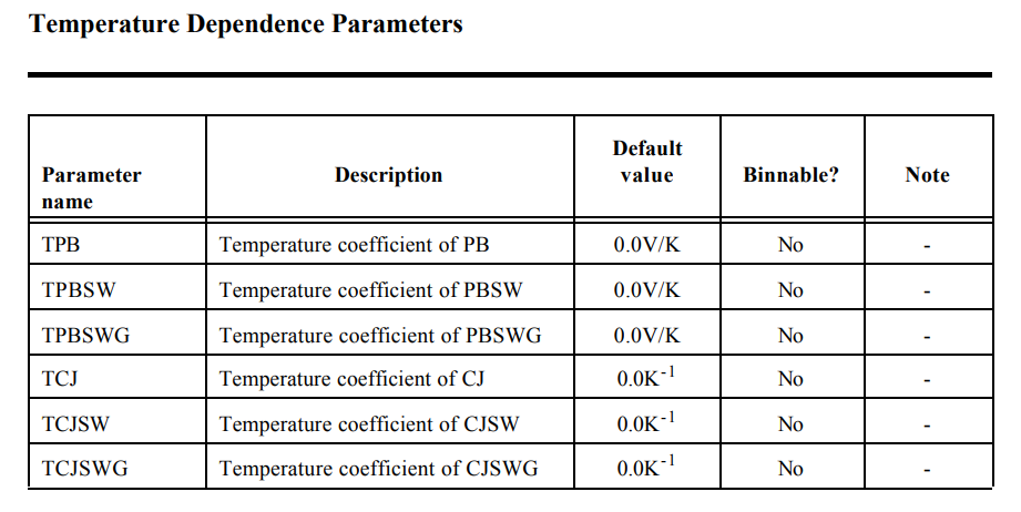
Temperature Dependence of Junction Diode CV
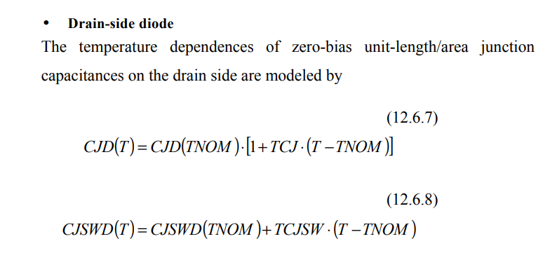
where TCJ and TCJSW are positive
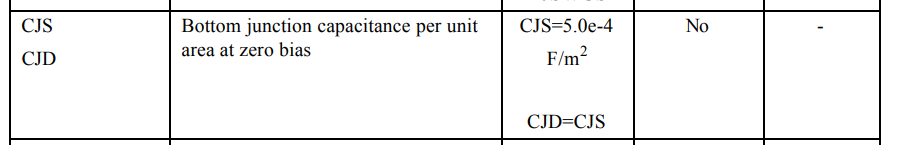
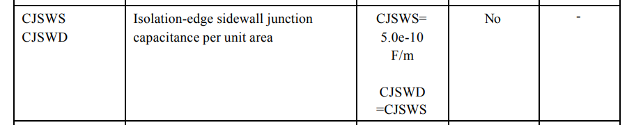
https://cmosedu.com/cmos1/BSIM4_manual.pdf
varactor
D=S=B varactor
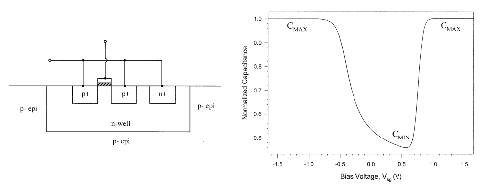
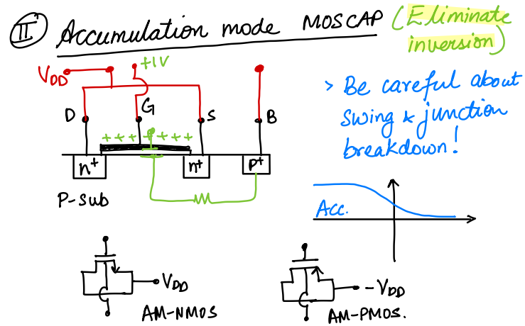
Inversion-mode (I-MOS)
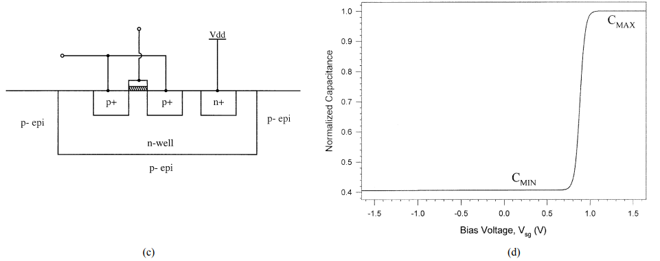
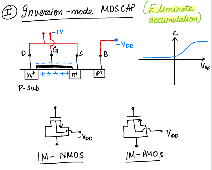
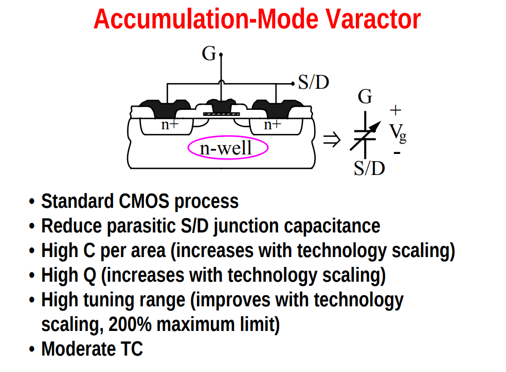
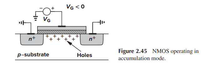
Accumulation-mode (A-MOS)
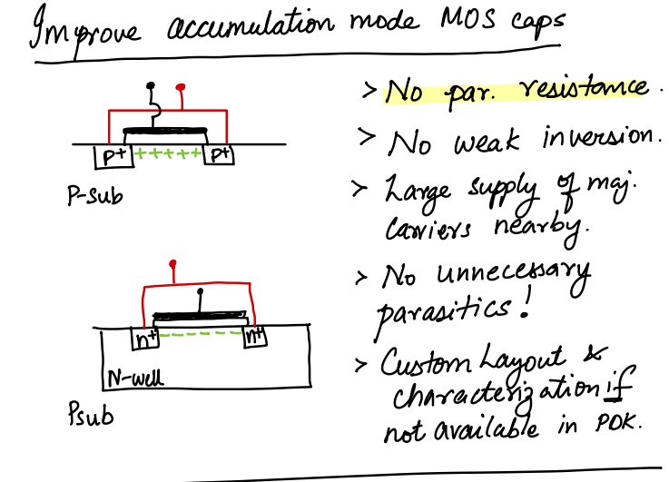
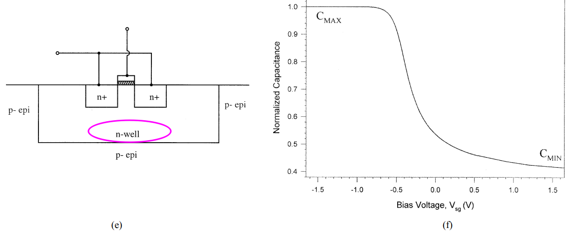
NMOS in NWELL, aka NMOS in N-Well varactor
Notice: S/D and NWELL are connected togethor in layout
PDK varactor
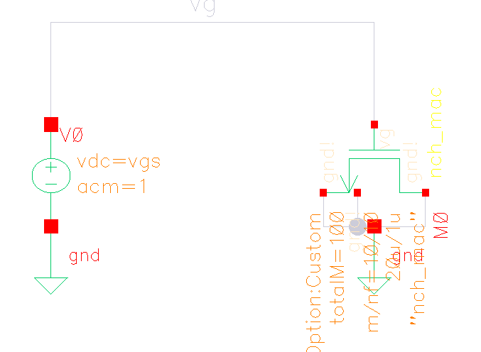
nmoscap: NMOS in N-Well varactor
- Base Band MOSCAP model (nmoscap) is built without effective series resistance (ESR) and effective series inductance (ESL) calibrations, which is for capacitance simulation only
- LC-Tank MOSCAP model (moscap_rf) is for frequency-dependent Q factor and capacitance simulations
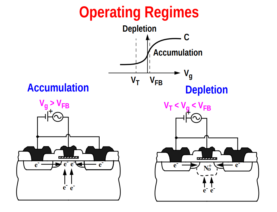
MOS Device as Capacitor
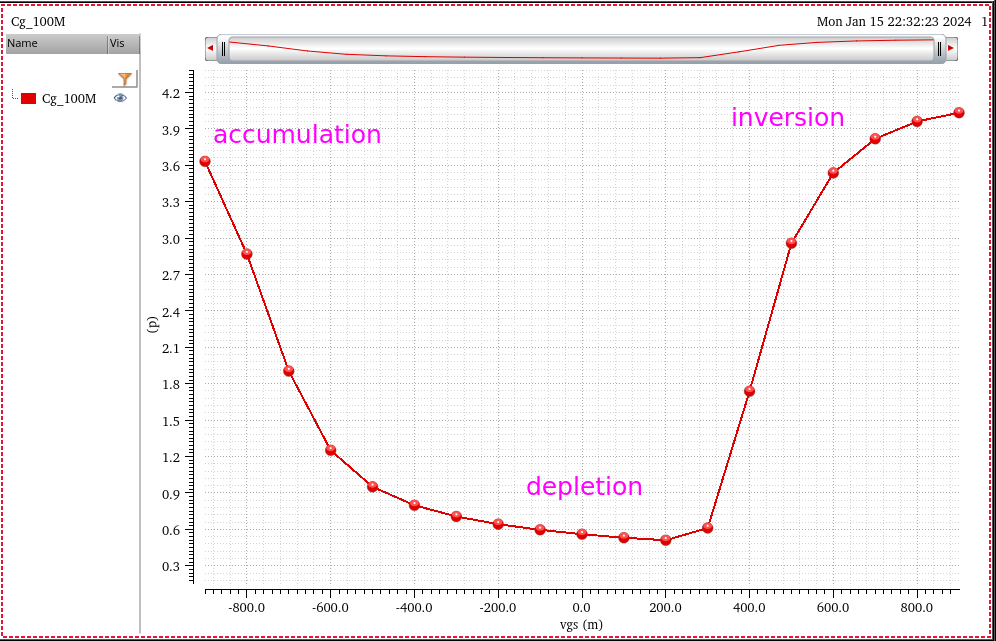
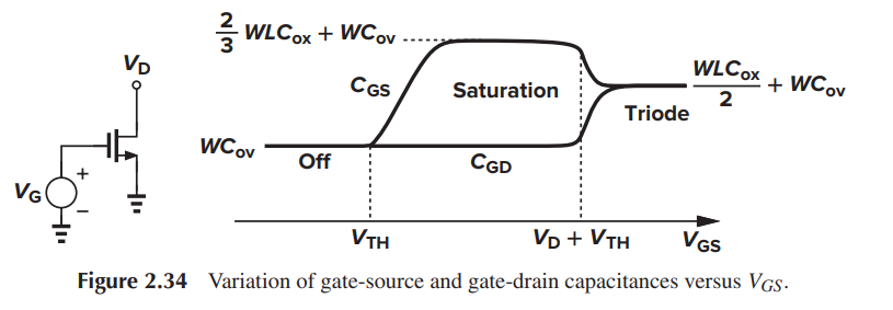
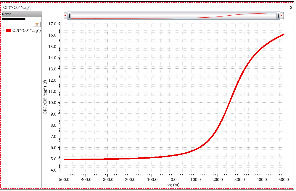
Voltage dependence
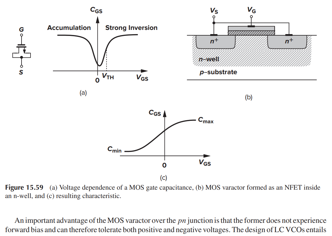
capacitance of MOS gate varies nonmonotonically with \(V_{GS}\)
"accumulation-mode" varactor varies monotonically with \(V_{GS}\)
reference
Aditya Varma Muppala. MOS Varactors | Oscillators 15 | MMIC 27 [https://youtu.be/LYCLZPQvIz0?si=yoSBZSD2j_wEx0zZ]
R. L. Bunch and S. Raman, "Large-signal analysis of MOS varactors in CMOS -G/sub m/ LC VCOs," in IEEE Journal of Solid-State Circuits, vol. 38, no. 8, pp. 1325-1332, Aug. 2003, doi: 10.1109/JSSC.2003.814416.
T. Soorapanth, C. P. Yue, D. K. Shaeffer, T. I. Lee and S. S. Wong, "Analysis and optimization of accumulation-mode varactor for RF ICs," 1998 Symposium on VLSI Circuits. Digest of Technical Papers (Cat. No.98CH36215), 1998, pp. 32-33, doi: 10.1109/VLSIC.1998.687993. URL: http://www-smirc.stanford.edu/papers/VLSI98s-chet.pdf
R. Jacob Baker, 6.1 MOSFET Capacitance Overview/Review, CMOS Circuit Design, Layout, and Simulation, Fourth Edition
B. Razavi, Design of Analog CMOS Integrated Circuits 2nd
Bing Sheu, TSMC. "Circuit Design using FinFETs" [https://www.nishanchettri.com/isscc-slides/2013%20ISSCC/TUTORIALS/ISSCC2013Visuals-T4.pdf]