Bandgap Reference
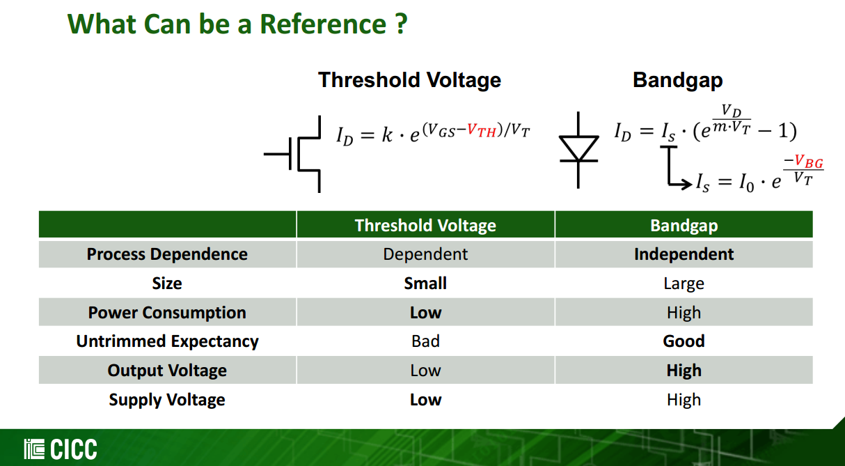
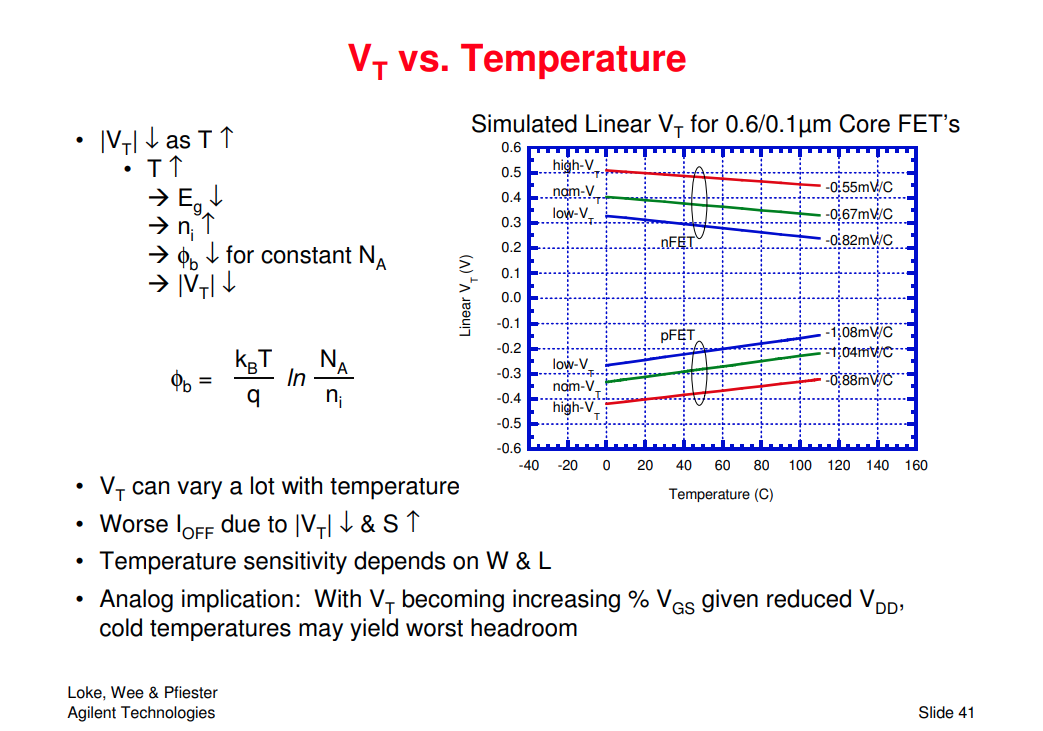
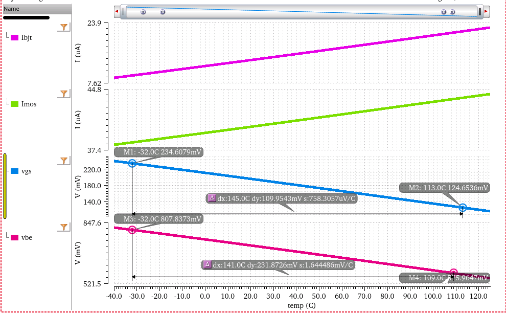
MOS VT vs. Temperature
[https://ewh.ieee.org/r5/denver/sscs/Presentations/2004_12_Loke.pdf]
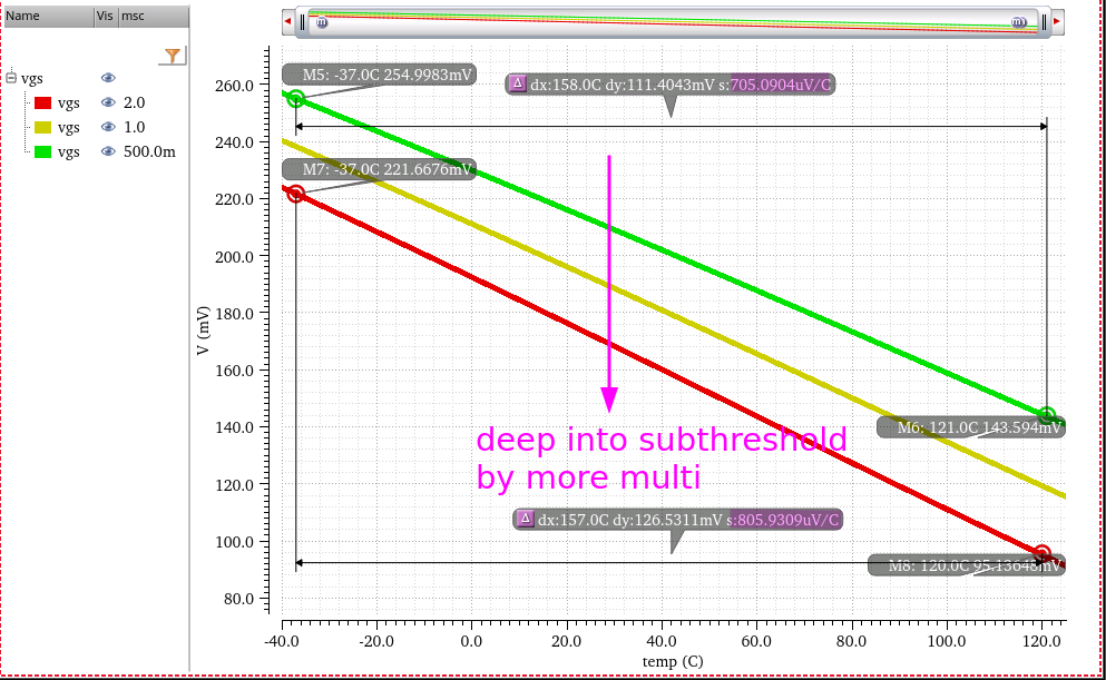
Subthreshold Conduction
By square-law, the Eq \(g_m = \sqrt{2\mu C_{ox}\frac{W}{L}I_D}\), it is possible to obtain a higer transconductance by increasing \(W\) while maintaining \(I_D\) constant. However, if \(W\) increases while \(I_D\) remains constant, then \(V_{GS} \to V_{TH}\) and device enters the subthreshold region. \[ I_D = I_0\exp \frac{V_{GS}}{\xi V_T} \]
where \(I_0\) is proportional to \(W/L\), \(\xi \gt 1\) is a nonideality factor, and \(V_T = kT/q\)
As a result, the transconductance in subthreshold region is \[ g_m = \frac{I_D}{\xi V_T} \]
which is \(g_m \propto I_D\)
PTAT with subthreshold MOS
MOS working in the weak inversion region ("subthreshold conduction") have the similar characteristics to BJTs and diodes, since the effect of diffusion current becomes more significant than that of drift current
Hongprasit, Saweth, Worawat Sa-ngiamvibool and Apinan Aurasopon. "Design of Bandgap Core and Startup Circuits for All CMOS Bandgap Voltage Reference." Przegląd Elektrotechniczny (2012): 277-280.
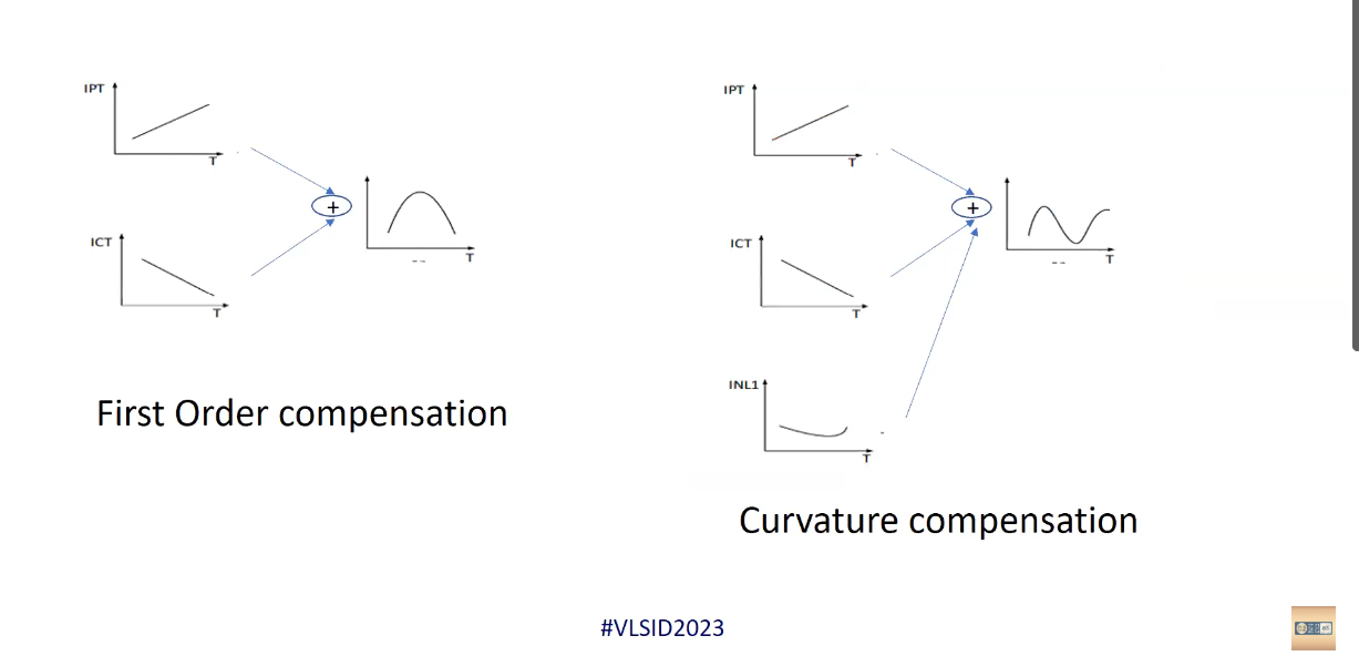
Curvature Compensation
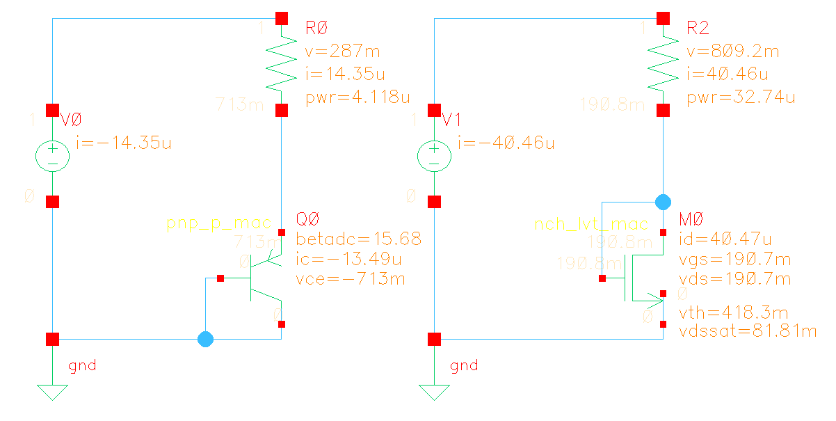
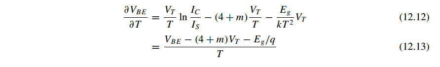
VBE
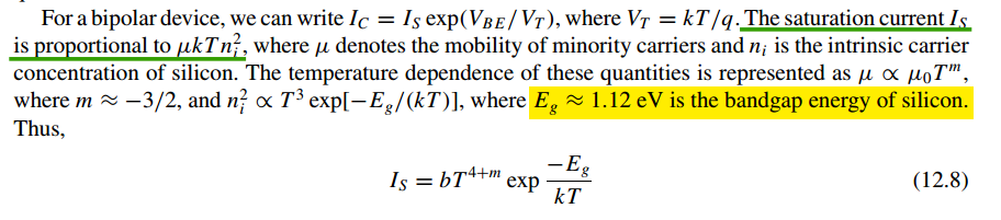
In advanced node, N4P, \(V_{BE}\) is about -1.45mV/K
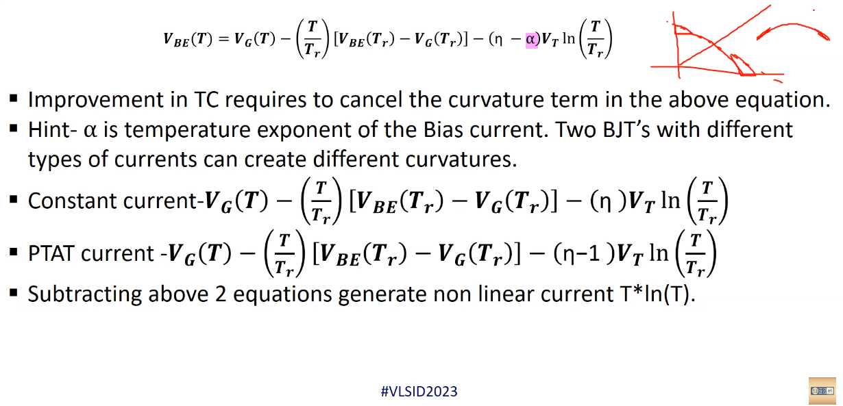
Assuming \(I_C\) is constant

Assuming \(I_C\) is PTAT, \(I_C = (V_T \ln n) / R_3\)
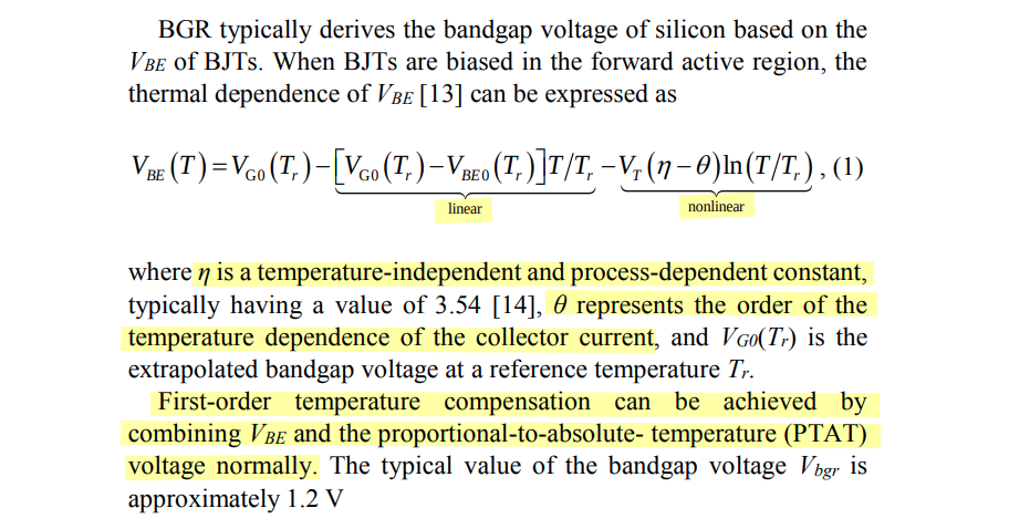
The first-order linear temperature dependence term of \(V_{BE}\) can be eliminated with IPTAT. \(V_T(\eta - \theta)\ln)T/T_r\) is the high-order nonlinear temperature-dependent term of \(V_{BE}\), which requires high-order curvature compensation
G. Zhu, Y. Yang and Q. Zhang, "A 4.6-ppm/°C High-Order Curvature Compensated Bandgap Reference for BMIC," in IEEE Transactions on Circuits and Systems II: Express Briefs, vol. 66, no. 9, pp. 1492-1496, Sept. 2019 [https://sci-hub.se/10.1109/TCSII.2018.2889808]
X. Fu, D. M. Colombo, Y. Yin and K. El-Sankary, "Low Noise, High PSRR, High-Order Piecewise Curvature Compensated CMOS Bandgap Reference," in IEEE Access, vol. 10, pp. 110970-110982, 2022 [https://ieeexplore.ieee.org/stamp/stamp.jsp?arnumber=9923910]
Tutorials | 08012023 | 1.2.1 Bandgap Voltage Regular [https://youtu.be/dz067SOX0XQ&t=6362]
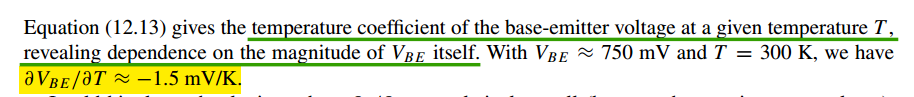
temperature coefficient
The parameter that shows the dependence of the reference voltage on temperature variation is called the temperature coefficient and is defined as: \[ TC_F=\frac{1}{V_{\text{REF}}}\left[ \frac{V_{\text{max}}-V_{\text{min}}}{T_{\text{max}}-T_{\text{min}}} \right]\times10^6\;ppm/^oC \]
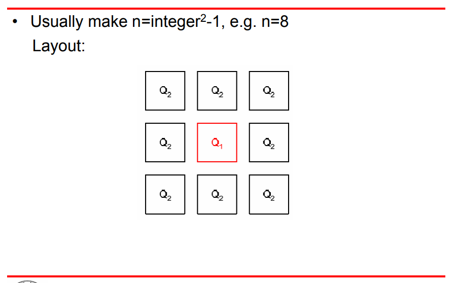
Choice of n
classic bandgap reference

\[ V_{bg} = \frac{\Delta V_{be}}{R_1} (R_1+R_2) + V_{be2} = \frac{\Delta V_{be}}{R_1} R_2 + V_{be1} \]
\[ V_{bg} = \left(\frac{\Delta V_{be}}{R_1} + \frac{V_{be1}}{R_2}\right)R_3 = \left(\frac{\Delta V_{be}}{R_1} R_2 + V_{be1}\right)\frac{R_3}{R_2} \]
OTA offset effect

\[\begin{align} V_{be1} &= \frac{kT}{q}\ln(\frac{I_{e1}}{I_{ss}}) \\ V_{be2} &= \frac{kT}{q}\ln(\frac{I_{e2}}{nI_{ss}}) \end{align}\]
Here, we assume \(I_e = I_c\)
Hence,
\[\begin{align} \Delta V_{be} &= \frac{kT}{q}\ln(n\frac{I_{e1}}{I_{e2}}) \\ &= \frac{kT}{q}\ln(n) + \frac{kT}{q}\ln(\frac{I_{e1}}{I_{e2}}) \\ &= \Delta V_{be,0} + \frac{kT}{q}\ln(\frac{I_{e1}}{I_{e2}}) \end{align}\]
Therefore,
\[\begin{align} V_{bg} &= \frac{\Delta V_{be}+V_{os}}{R_2}(R_1+R_2) + V_{be2} \\ &= \alpha \Delta V_{be,0} + \alpha \frac{kT}{q}\ln(\frac{I_{e1}}{I_{e2}}) + \alpha V_{os} + \frac{kT}{q}\ln(\frac{I_{e2}}{nI_{ss}}) \\ &= \alpha \Delta V_{be,0} + \alpha \frac{kT}{q}\ln(\frac{I_{e1}}{I_{e2}}) + \alpha V_{os} + \frac{kT}{q}\ln(\frac{I_{e2,0}}{nI_{ss}})+\frac{kT}{q}\ln(\frac{I_{e2}}{I_{e2,0}}) \end{align}\]
where \(\alpha = \frac{R_1+R_2}{R_2}\)
We omit the last part \[\begin{align} V_{bg} &\approx \alpha \Delta V_{be,0} + \alpha \frac{kT}{q}\ln(\frac{I_{e1}}{I_{e2}}) + \alpha V_{os} + \frac{kT}{q}\ln(\frac{I_{e2,0}}{nI_{ss}}) \\ &= \alpha \Delta V_{be,0} + V_{be2,0} + \alpha \left(V_{os} + \frac{kT}{q}\ln(\frac{I_{e1}}{I_{e2}})\right) \\ &= V_{bg,0} + \alpha \left(V_{os} + \frac{kT}{q}\ln(\frac{I_{e1}}{I_{e2}})\right) \end{align}\]
i.e. the bg variation due to OTA offset \[ \Delta V_{bg} \approx \alpha \left(V_{os} + \frac{kT}{q}\ln(\frac{I_{e1}}{I_{e2}})\right) \]
\(V_{os} \gt 0\)
\(I_{e1} \gt I_{e2}\): \(\Delta V_{bg} \gt \alpha V_{os}\)
\(V_{os} \lt 0\)
\(I_{e1} \lt I_{e2}\): \(\Delta V_{bg} \lt \alpha V_{os}\)
OTA with chopper


\(I_{e1}\), \(I_{e2}\)
\[\begin{align} V_{ip} &= V_{im} + V_{os} \\ \frac{V_{bg}-V_{ip}}{R_2} &= I_{e2} \qquad \frac{V_{bg}-V_{im}}{R_2} = I_{e1} \\ V_{ip} &= I_{e2}R_1 + V_T\frac{I_{e2}}{nI_S} \qquad V_{im} = V_T\frac{I_{e1}}{I_S} \end{align}\] where \(V_T = \frac{kT}{q}\)
we obtain \[ I_{e1} = \frac{V_T\ln n}{R_1} + V_{os}\left(\frac{1}{R_1} + \frac{1}{R_2} \right) - \frac{1}{R_1}\cdot V_T\ln\left(1- \frac{V_{os}}{R_2I_{e1}} \right) \]
we omit the last part \[\begin{align} I_{e1} &= I_{e0} + V_{os}\left(\frac{1}{R_1} + \frac{1}{R_2} \right) \\ I_{e2} &= I_{e1} - \frac{V_{os}}{R_2} = I_{e0} + \frac{V_{os}}{R_1} \end{align}\] where \(I_{e0} = \frac{\Delta V_{be}}{R_1}\), \(\Delta V_{be}=V_T\ln n\)
That is, both \(I_{e1}\) and \(I_{e2}\) are proportional to \(V_{os}\)
\[ I_{e,tot} = I_{e1} + I_{e2} = 2I_{e0} + V_{os}\left(\frac{2}{R_1} + \frac{1}{R_2} \right) = 2I_{e0} + V_{os}\frac{R_1+2R_2}{R_1R_2} = I_0 + \frac{V_{os}}{R_E} \]
where \(I_0 = 2I_{e0}\), \(R_E = \frac{R_1R_2}{R_1+2R_2}\)
\(I_{e1}\) and \(I_{e2}\) can also be expressed as \[\begin{align} I_{e1} &= I_{e0} + V_{os}\left(\frac{1}{R_1} + \frac{1}{2R_2} \right) + \frac{V_{os}}{2R_2} \\ I_{e2} &= I_{e0} + V_{os}\left(\frac{1}{R_1} + \frac{1}{2R_2} \right) - \frac{V_{os}}{2R_2} \end{align}\] i.e., \(\Delta I_{e,cm} = V_{os}\left(\frac{1}{R_1} + \frac{1}{2R_2} \right)\) and \(\Delta I_{e,dif} =\frac{V_{os}}{2R_2}\)
bandgap output voltage is
\[\begin{align} V_{bg} &= V_T \ln \frac{I_{e1}}{I_s} + I_{e1}R_2 \\ &= V_T \ln \frac{I_{e0} + V_{os}\left(\frac{1}{R_1} + \frac{1}{R_2} \right)}{I_s} + I_{e1}R_2 \\ &= V_T \ln \frac{I_{e0} + V_{os}\left(\frac{1}{R_1} + \frac{1}{R_2} \right)}{I_s} + I_{e0}R_2 + V_{os}\frac{R_1+R_2}{R_1} \\ &= I_{e0}R_2 + V_T \ln \frac{I_{e0}}{I_s} + V_T\ln\left(1+\frac{V_{os}\left(\frac{1}{R_1} + \frac{1}{R_2} \right)}{I_{e0}} \right) + V_{os}\frac{R_1+R_2}{R_1} \\ &= V_{bg0} + V_T\ln\left(1+\frac{V_{os}\left(\frac{1}{R_1} + \frac{1}{R_2} \right)}{I_{e0}} \right) + V_{os}\frac{R_1+R_2}{R_1} \end{align}\]
Therefore, the averaged output of bandgap
\[ V_{bg,avg} = V_{bg0} +\frac{1}{2}V_T\ln\left(1-\frac{V_{os}^2\left(\frac{1}{R_1} + \frac{1}{R_2} \right)^2}{I_{e0}^2} \right) \lt V_{bg0} \]
\(V_{bg,avg} \lt V_{bg0}\) due to nonlinearity of BJT
reference
ECEN 607 (ESS) Bandgap Reference: Basics URL:https://people.engr.tamu.edu/s-sanchez/607%20Lect%204%20Bandgap-2009.pdf
CICC 2023 Session 12: Forum: Recent Progress in LDOs and Voltage, Current, and Timing References
- Jae-Yoon Sim, POSTECH. 12-2: Design of Ultra-low-power Bandgap Reference Circuits
- Inhee Lee, University of Pittsburgh. 12-3: Sub-μW Non-Bandgap Voltage References