Device Aging & Reliability
Terminology
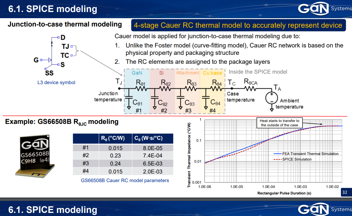
The most accurate method to calculate the degradation of transistors is the SPICE-level simulation of the whole netlist with application programming interface (API) and industry-standard stress process models
MOSRA: MOSFET reliability analysis Synopsys
RelXpert: Cadence
TMI: TSMC Model Interface, TSMC
OMI: Open Model Interface, Si2 standard,
The Silicon Integration Initiative (Si2) Compact Model Coalition has released the Open Model Interface, an Si2 standard, C-language application programming interface that supports SPICE compact model extensions.OMI allows circuit designers to simulate and analyze such important physical effects as self-heating and aging, and perform extended design optimizations. It is based on TMI2, the TSMC Model Interface, which was donated to Si2 by TSMC in 2014.
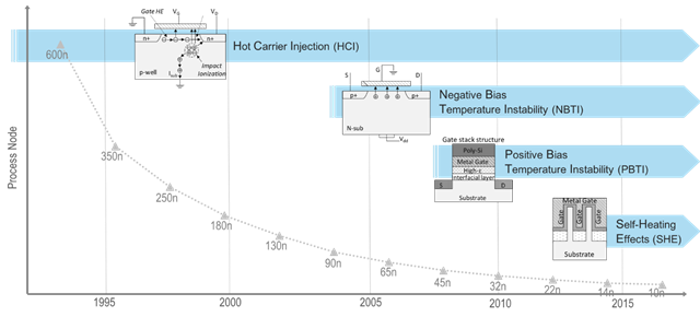
- TDDB: Time-Dependent Dielectric Breakdown
- HCI: Hot Carrier injection
- BTI: Bias Temperature Instability
- NBTI: Negative Bias Temperature Instability
- PBTI: Positive Bias Temperature Instability
- SHE: Self-Heating Effect
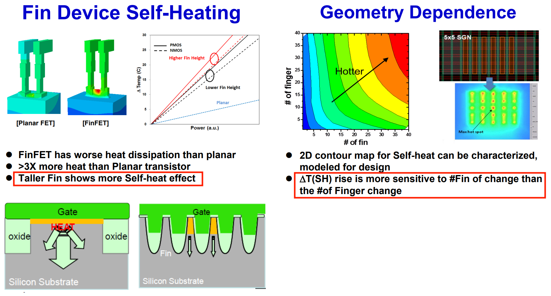
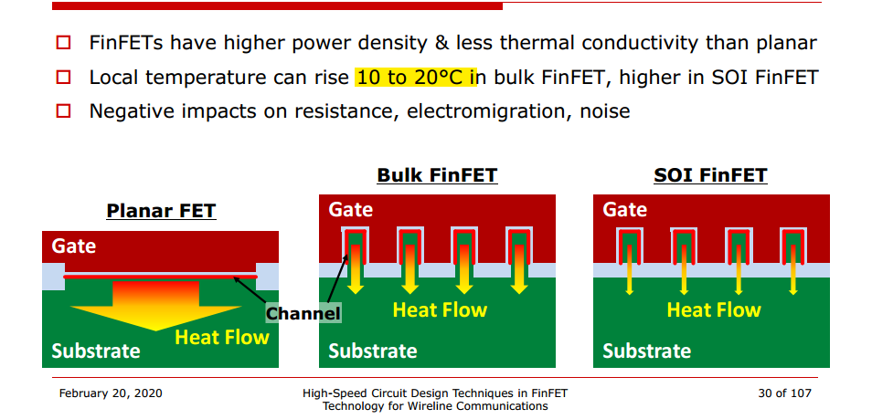
Self-Heating Effect (SHE)
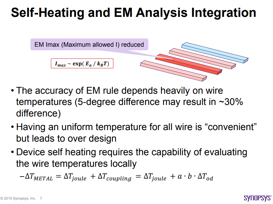
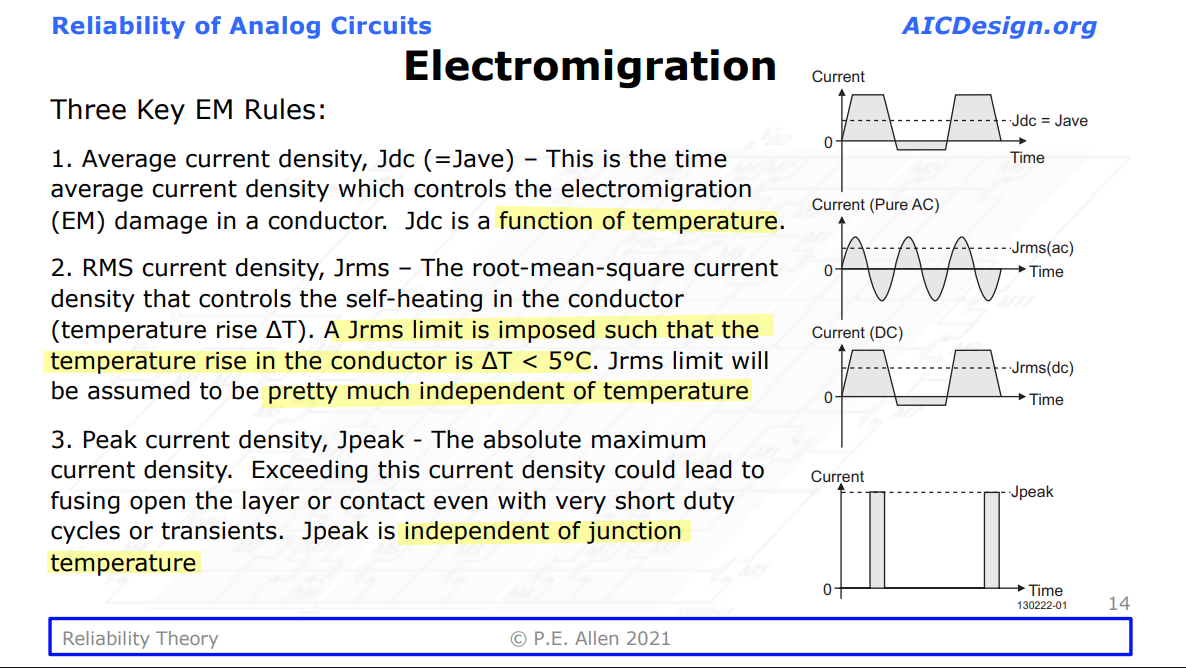
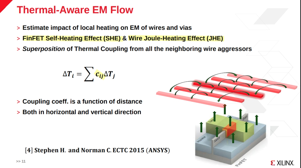
Self-heating effect (SHE) is composed of FEOL self-heat and BEOL self-heat, both contribute to the \(\Delta T\)
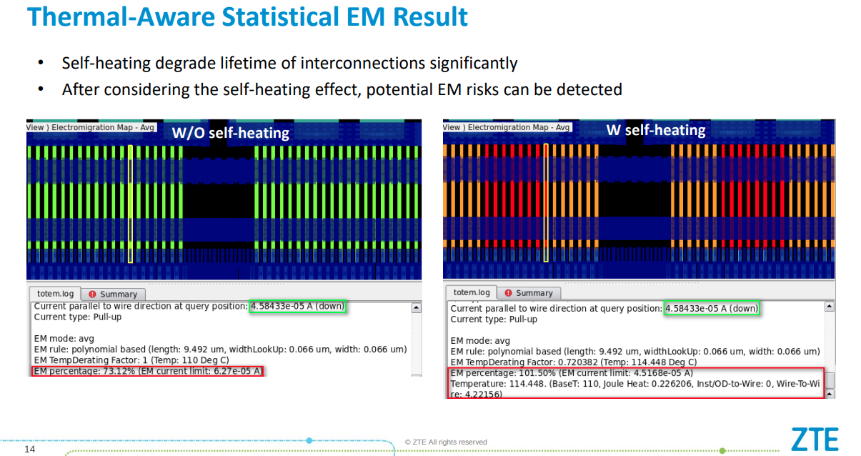
aging w/i SHE
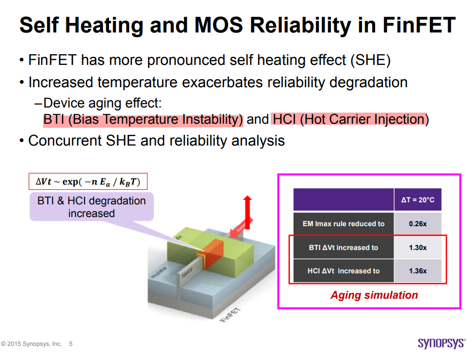
EM w/i SHE
Junjie Chen, Keqing Ouyang ZTE SANECHIPS. Challenges and Solutions of PI Signoff for Next Generation Large Scale Chips with TSMC 7nm Process Technology [pdf]
Thermal coupling
Jae-Gyung Ahn Oct 3rd 2019 Xlinx. Design For Thermal Reliability in 7nm [https://www.ieee-edps.com/archives/2019/c/0300ahn.pdf]
M. Lofrano et al., "Towards accurate temperature prediction in BEOL for reliability assessment (Invited)," 2023 IEEE International Reliability Physics Symposium (IRPS), Monterey, CA, USA, 2023, pp. 1-7, doi: 10.1109/IRPS48203.2023.10117701
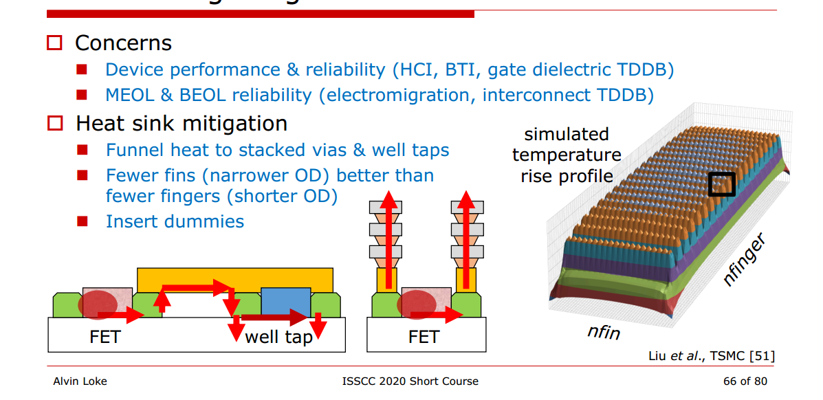
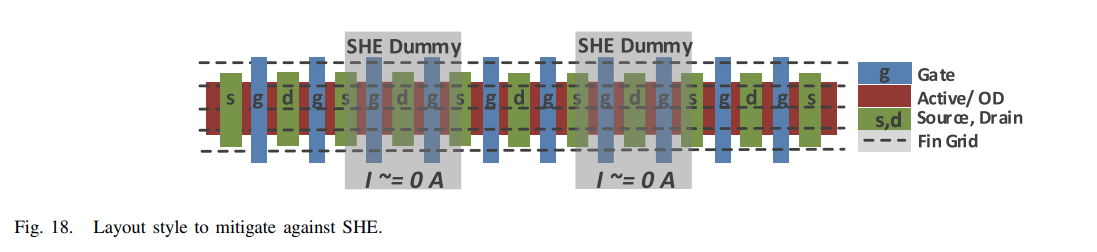
Mitigating Self-Heating
A. Loke, "Short Course: Device and Physical Design Considerations for Circuits in FinFET Technology," 2020 IEEE International Solid-State Circuits Conference - (ISSCC), San Francisco, CA, USA, 2020 [pdf]
J. E. Proesel, "Short Course: High-Speed and Mixed-Signal Circuit Design Techniques in FinFET Technology for Wireline and Optical Interface Applications," 2020 IEEE International Solid-State Circuits Conference - (ISSCC), San Francisco, CA, USA, 2020
guard ring
closer OD help reduce dT
extended gate
source/drain metal stack
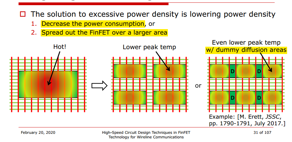
M. Erett et al., "A 0.5–16.3 Gbps Multi-Standard Serial Transceiver With 219 mW/Channel in 16-nm FinFET," in IEEE Journal of Solid-State Circuits, vol. 52, no. 7, pp. 1783-1797, July 2017 [https://sci-hub.se/10.1109/JSSC.2017.2702711]
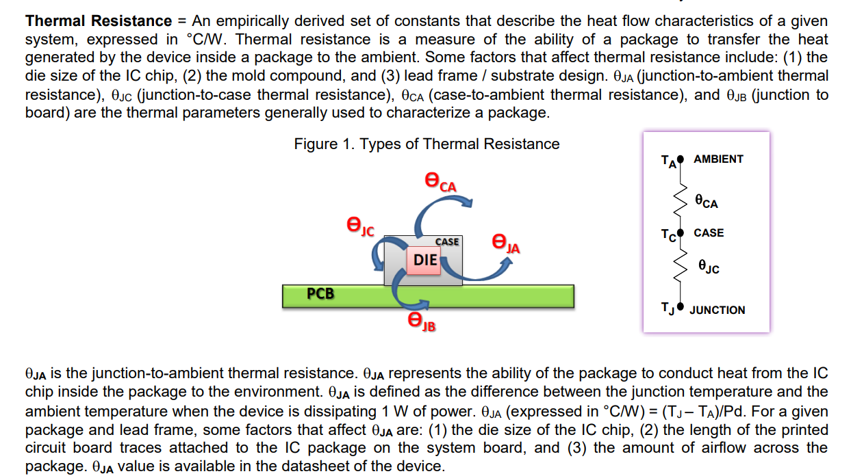
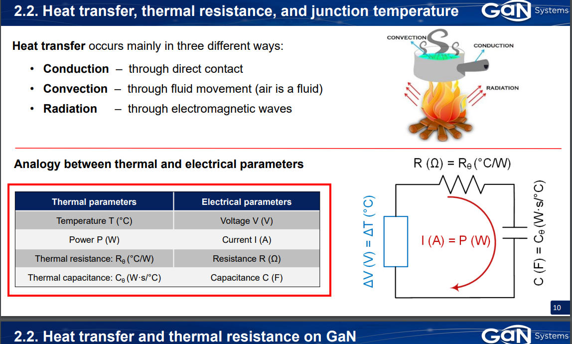
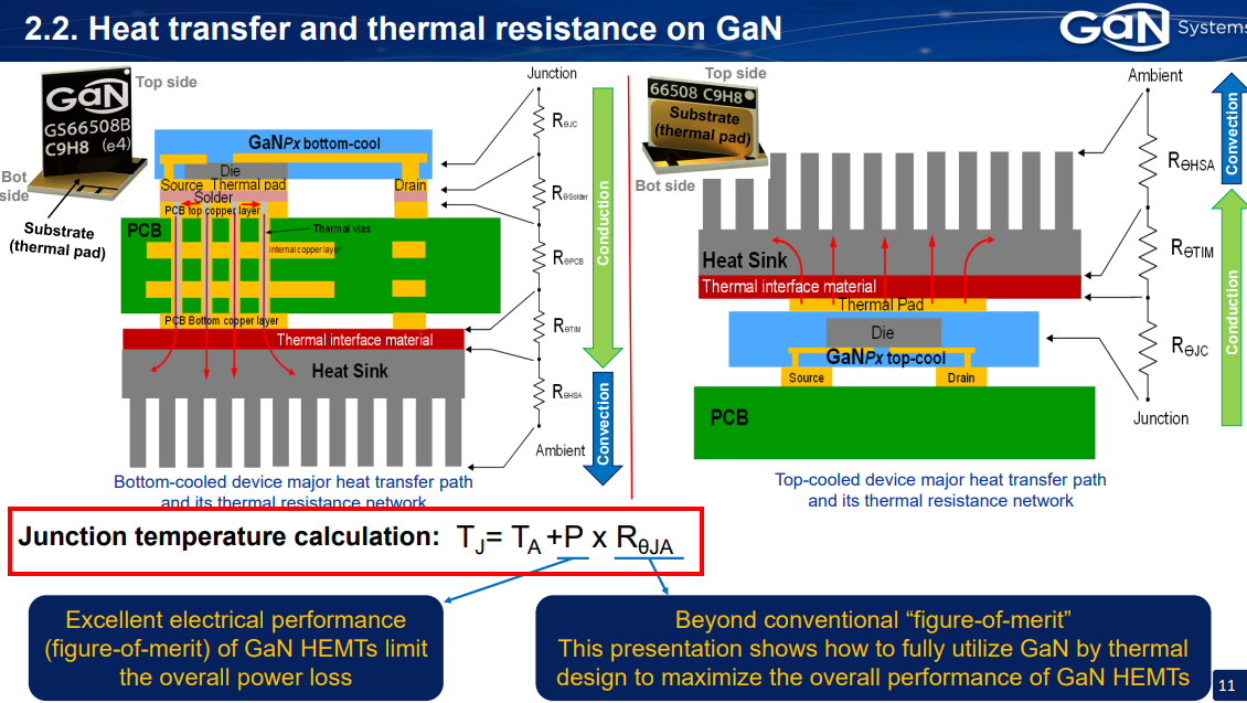
Heat transfer, thermal resistance
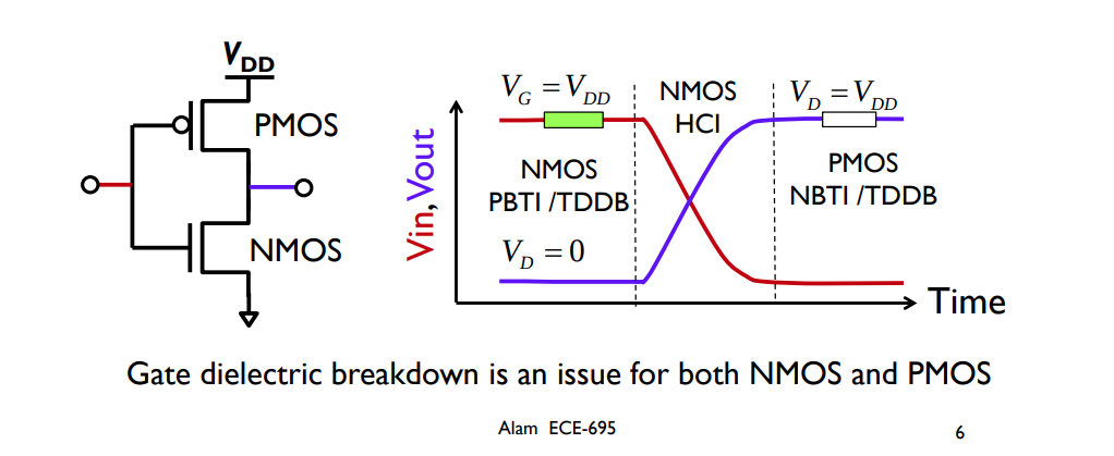
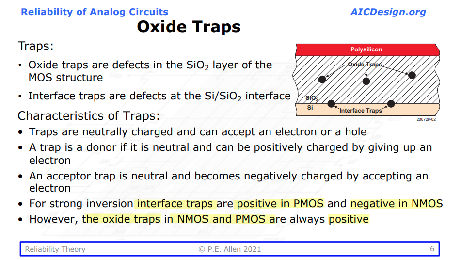
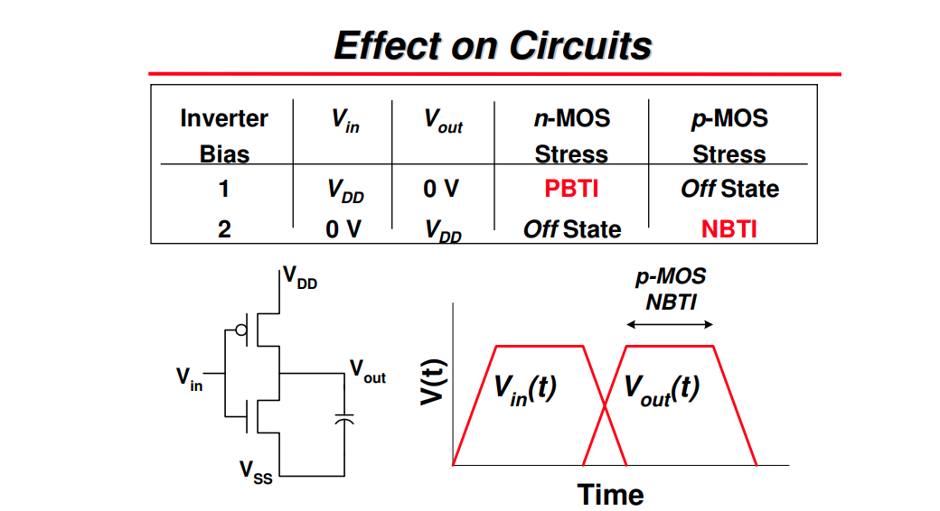
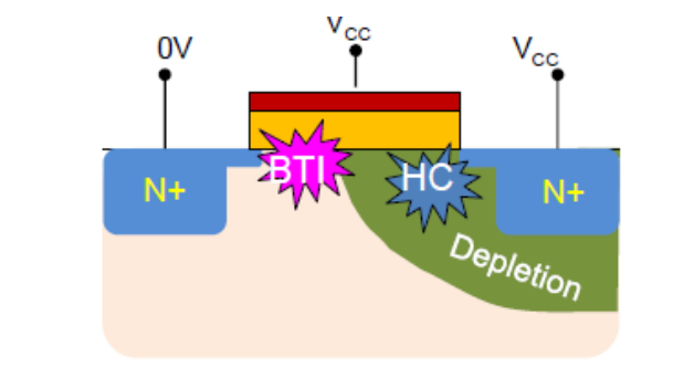
Bias Temperature Instability (BTI)
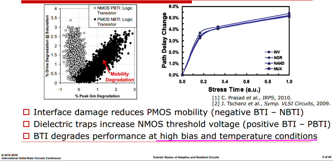
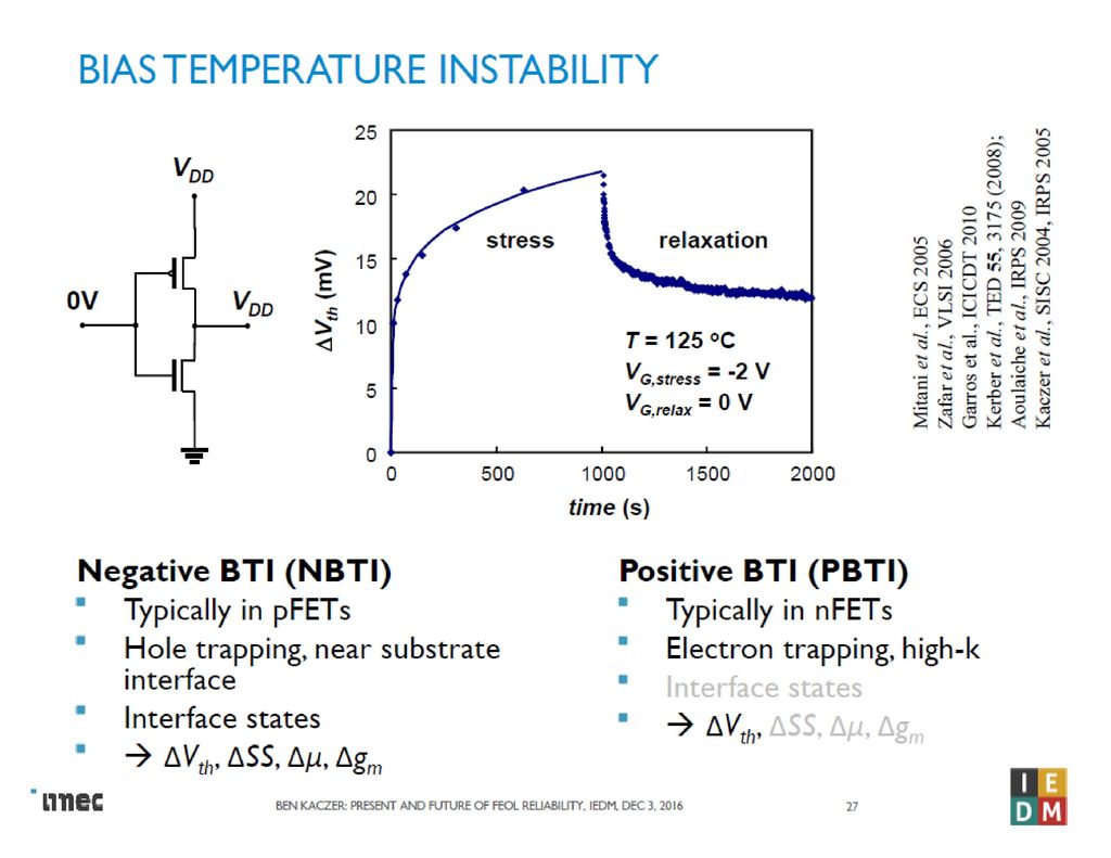
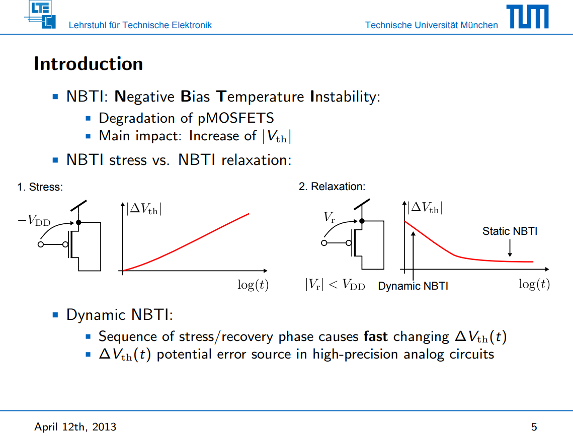
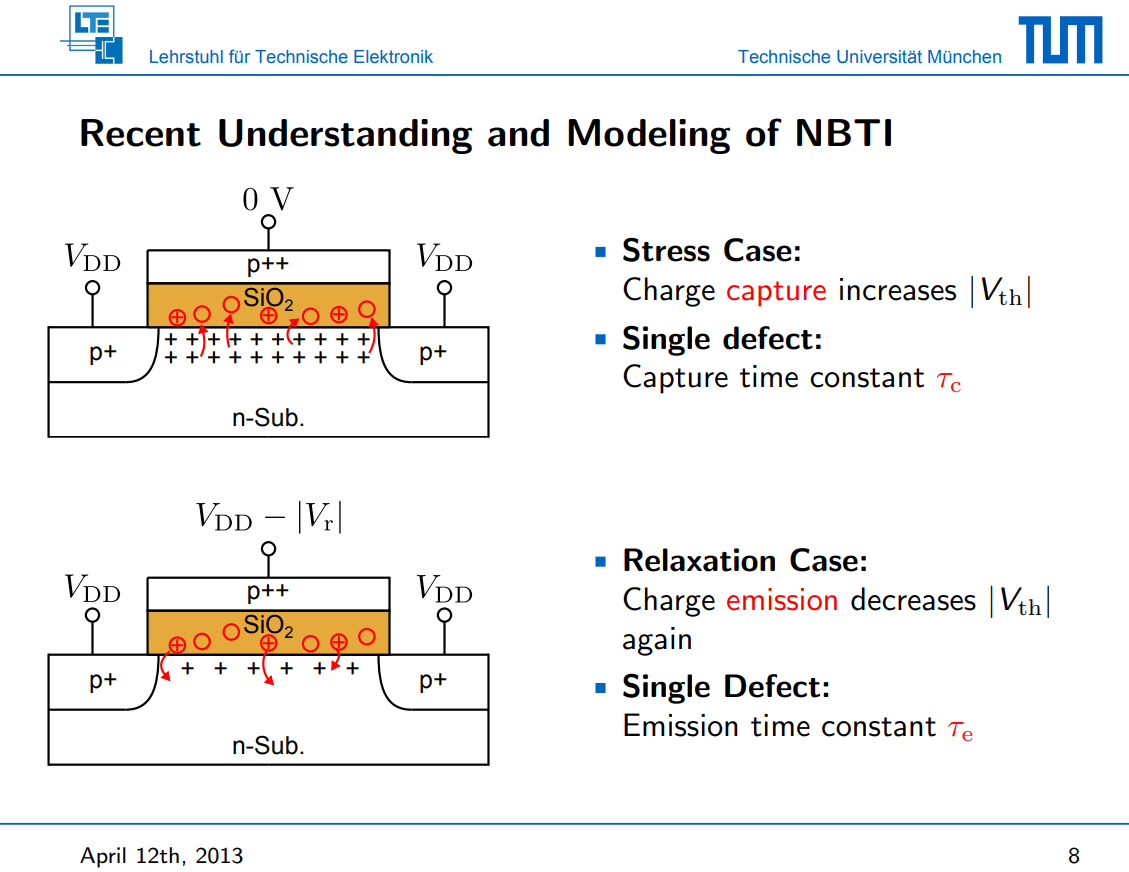
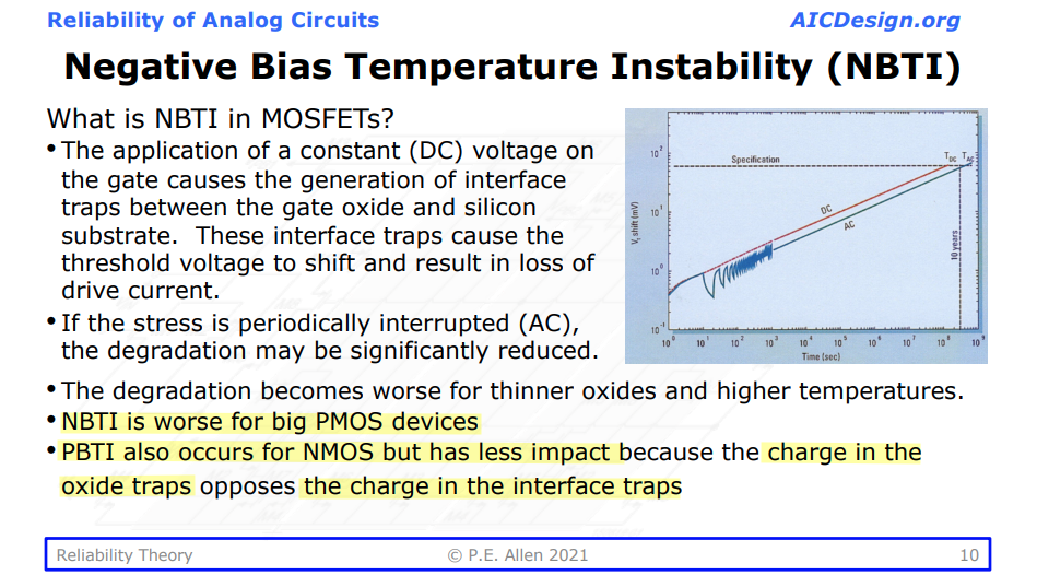
BTI occurs predominantly in PMOS (or p-type or p channel) transistors and causes an increase in the transistor's absolute threshold voltage.
Stress in the case of NBTI means that the PMOS transistor is in inversion; that means that its gate to body potential is substantially below 0 V for analogue circuits or at VGB = −VDD for digital circuits
Higher voltages and higher temperatures both have an exponential impact onto the degradation, induced by NBTI.
NBTI will be accelaerated with thinner gate oxide, at a high temperature and at a high electric field across the oxide region.
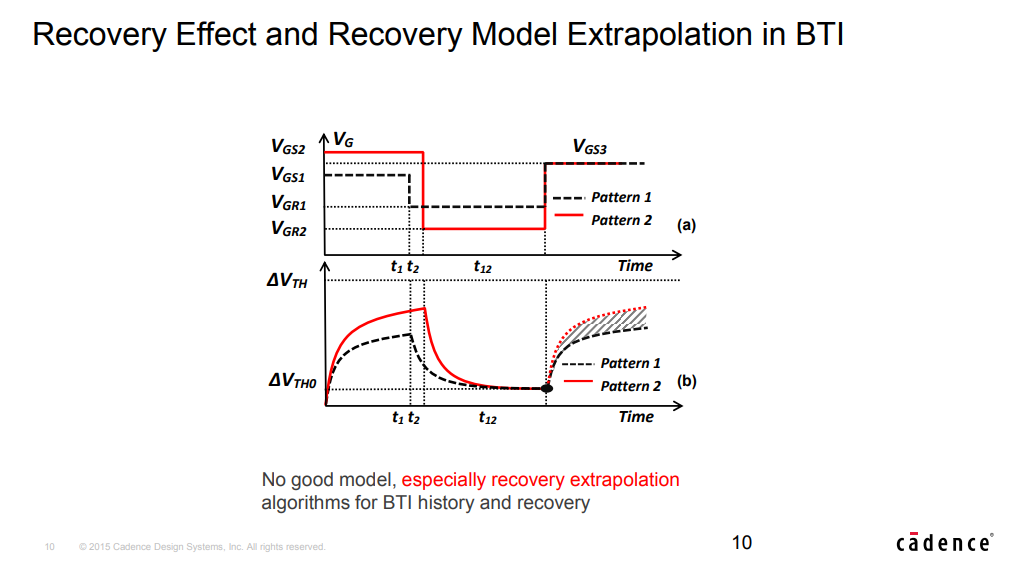
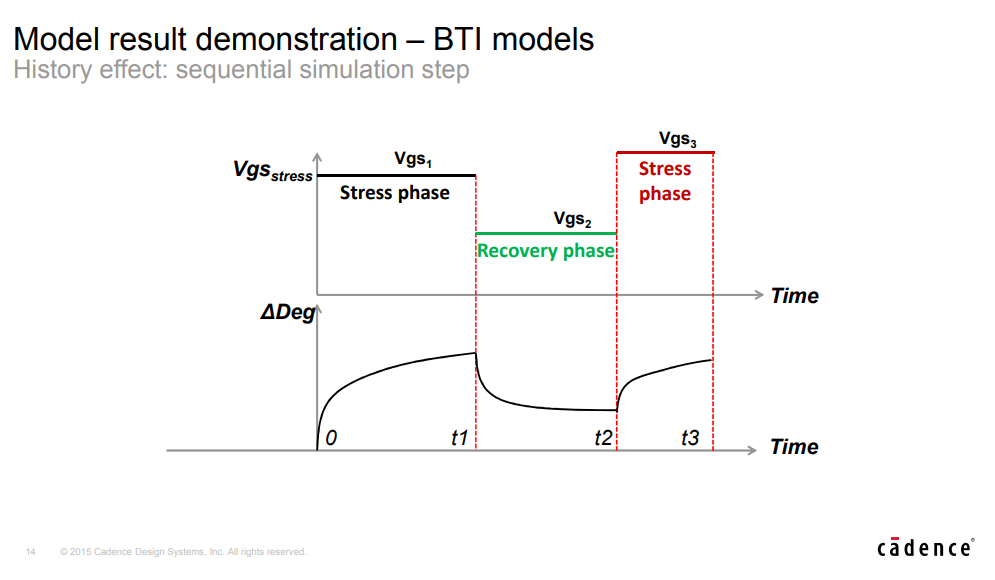
During recovery phase where the gate voltage of pMOS is high and stress is removed, the H atoms in the gate oxiede diffuse back to Si-SiO2 interface and the recombination of Si-H bonds reduces the threshold voltage of pMOS.
The net result is an increase in the magnitude of the device threshold voltage |Vt|, and a degradation of the channel carrier mobility.
Caution: The aging model provided by fab may NOT contain recovry effect
PBTI
Dieter K. Schroder. Negative Bias Temperature Instability (NBTI) Physics, Materials, Process, and Circuit Issues [https://ewh.ieee.org/r5/denver/sscs/Presentations/2005_08_Schroder.pdf]
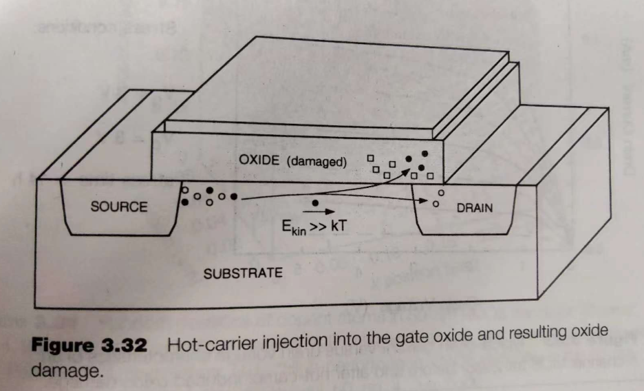
Hot Carrier Degradation (HCI)
Short-channel MOSFETs may exprience high lateral electric fields if the drain-source voltage is large. while the average velocity of carriers saturate at high fields, the instantaneous velocity and hence the kinetic energy of the carriers continue to increase, especially as they accelerate toward the drain. These are called hot carriers.
In nanometer technologies, hot carrier effects have subsided. This is because the energy required to create an electron-hole pair, \(E_g \simeq 1.12 eV\), is simply not available if the supply voltage is around 1V.
\[ F_E= E \cdot q \]
\[\begin{align} E_k &= F_E \cdot s \\ &= E \cdot q \cdot s \end{align}\]
Electrons and holes gaining high kinetic energies in the electric field (hot carriers) may be injected into the gate oxide and cause permanent changes in the oxide-interface charge distribution, degrading the current-voltage characteristics of the MOSFET.
The channel hot-electron (CHE) effect is caused by electons flowing in the channel region, from the source to the drain. This effect is more pronounced at large drain-to-source voltage, at which the lateral electric field in the drain end of the channel accelerates the electrons.
Four different hot carrier injectoin mechanisms can be distinguished: - channel hot electron (CHE) injection - drain avalanche hot carrier (DAHC) injection - secondary generated hot electron (SGHE) injection - substrate hot electron (SHE) injection
HCI is more of a drain-localized mechanism, and is primarily a carrier mobility degradation (and a Vt degradation if the device is operated bi-directionally).
For smaller transistor dimensions, CHE dominates the hot carrier degradation effect
The hot-carrier induced damage in nMOS transistors has been found to result in either trapping of carriers on defect sites in the oxide or the creation of interface states at the silicon-oxide interface, or both.
The damage caused by hot-carrier injection affects the transistor characteristics by causing a degradation in transconductance, a shift in the threshold voltage, and a general decrease in the drain current capability.
HCI seems to have just a weak temperature dependency
Unlike BTI, it seems to be no or just little recovery. As holes are much "cooler" (i.e. heavier) than electrons, the channel hot carrier effect in nMOS devices is shown to be more significant than in pMOS devices.
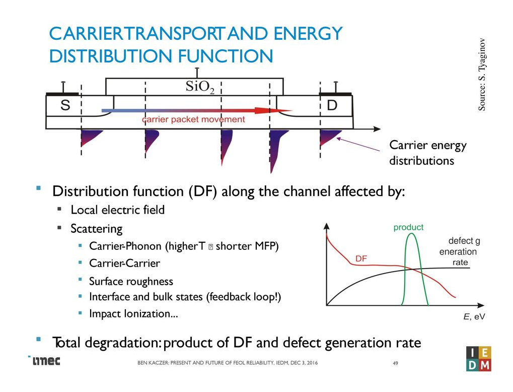
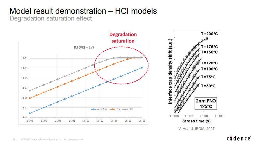
Degradation saturation effect
HCI model can reproduce the saturation effect if stress time is long enough
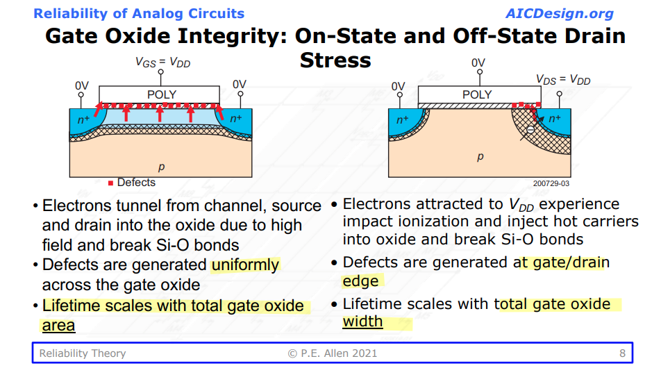
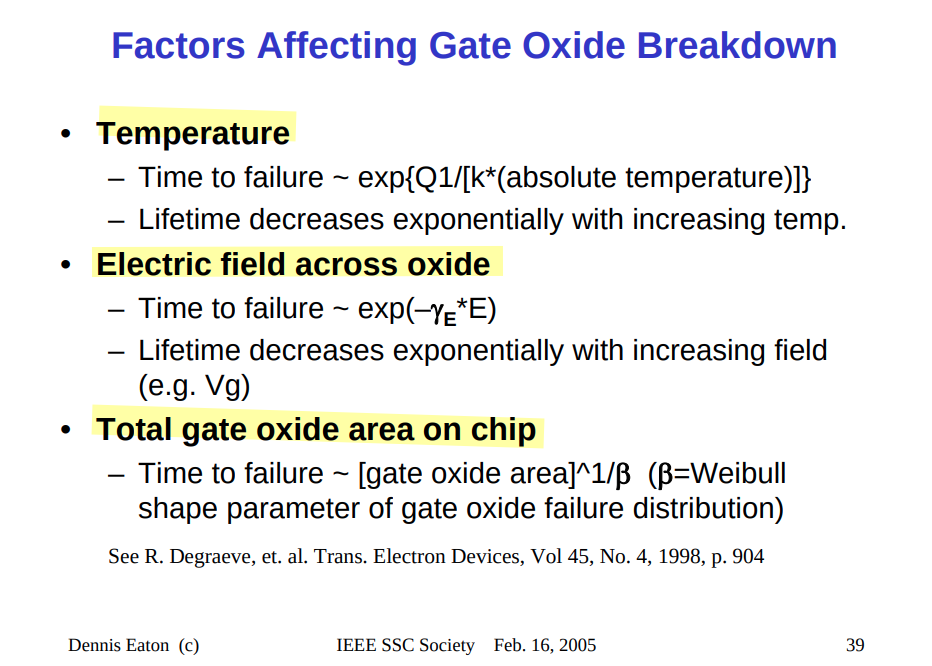
Gate Oxide Integrity (GOI)
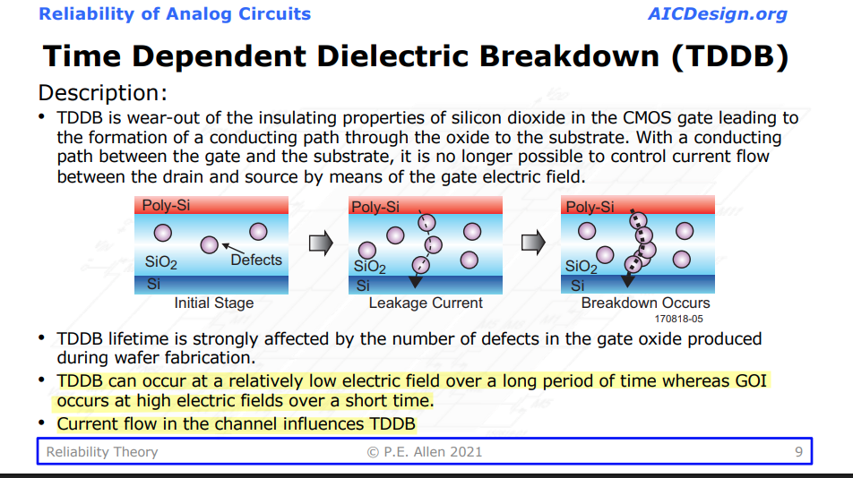
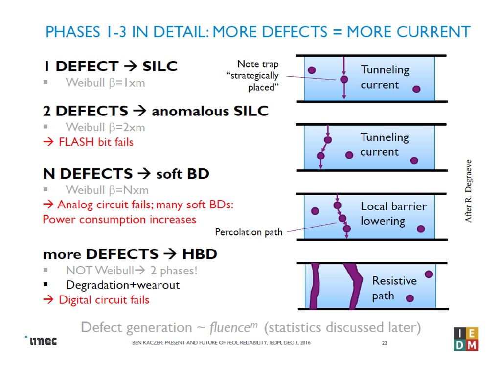
Time dependent dielectric breakdown (TDDB)
M. A. Alam, ECE 695A Reliability Physics of Nanotransistors [link], [https://nanohub.org/resources/17208/download/2013.03.01-ECE695A-L21.pdf]
K. Yang, R. Zhang, T. Liu, D. -H. Kim and L. Milor, "Optimal Accelerated Test Regions for Time- Dependent Dielectric Breakdown Lifetime Parameters Estimation in FinFET Technology," 2018 Conference on Design of Circuits and Integrated Systems (DCIS), Lyon, France, 2018 [https://par.nsf.gov/servlets/purl/10104486]
Scaling drive more concerns in TDDB
waveform-dependent nature
The figure below illustrates the waveform-dependent nature of these mechanisms – as described earlier, BTI and HCI depend upon the region of active device operation. The slew rate of the circuit inputs and output will have a significant impact upon these mechanisms, especially HCI.
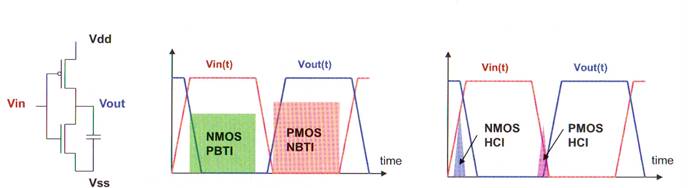
- Negative bias temperature instability (NBTI). This is caused by constant electric fields degrading the dielectric, which in turn causes the threshold voltage of the transistor to degrade. That leads to lower switching speeds. This effect depends on the activity level of the circuits, with heavier impact on parts of the design that don’t switch as often, such as gated clocks, control logic, and reset, programming and test circuitry.
- Hot carrier injection (HCI). This is caused by fast-moving electrons inserting themselves into the gate and degrading performance. It primarily occurs on higher-voltage modes and fast switching signals.
- longer channel length help both BTI and HCI
- larger \(V_{ds}\) help BTI, but hurt HCI
- lower temperature help BTI of core device, but hurt that of IO device for 7nm FinFET
aging model
MOSRA
MOSRA is a 2-step simulation: 1) Age computation, 2) Post-age analysis
TMI
BTI recovery effect NOT included for N7
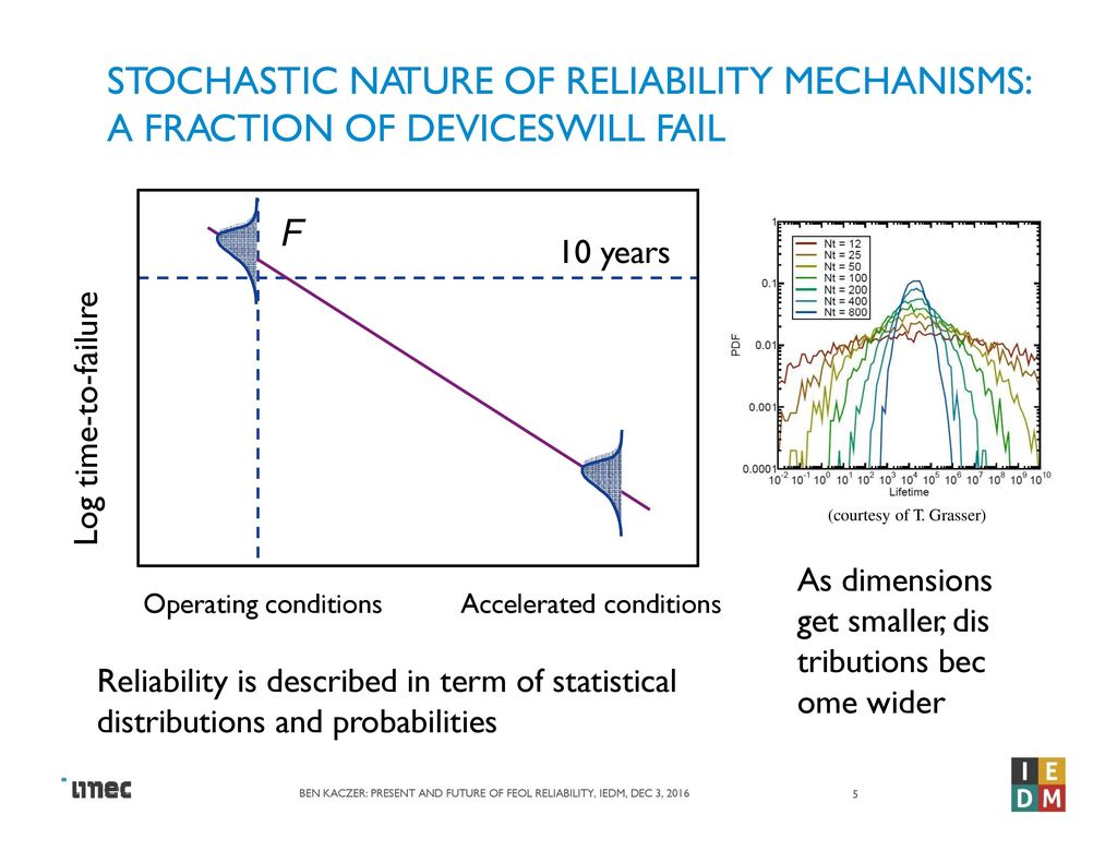
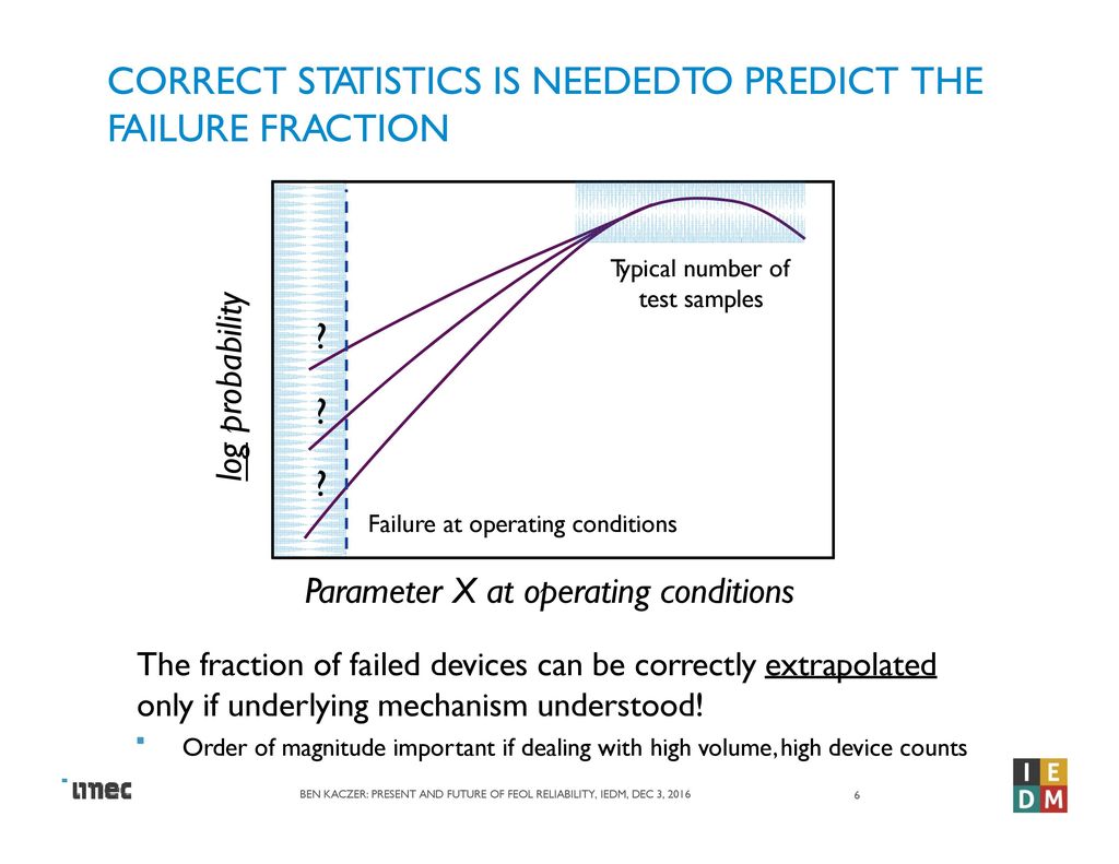
Stochastic Nature of Reliability Mechanisms
A fraction of devices will fail
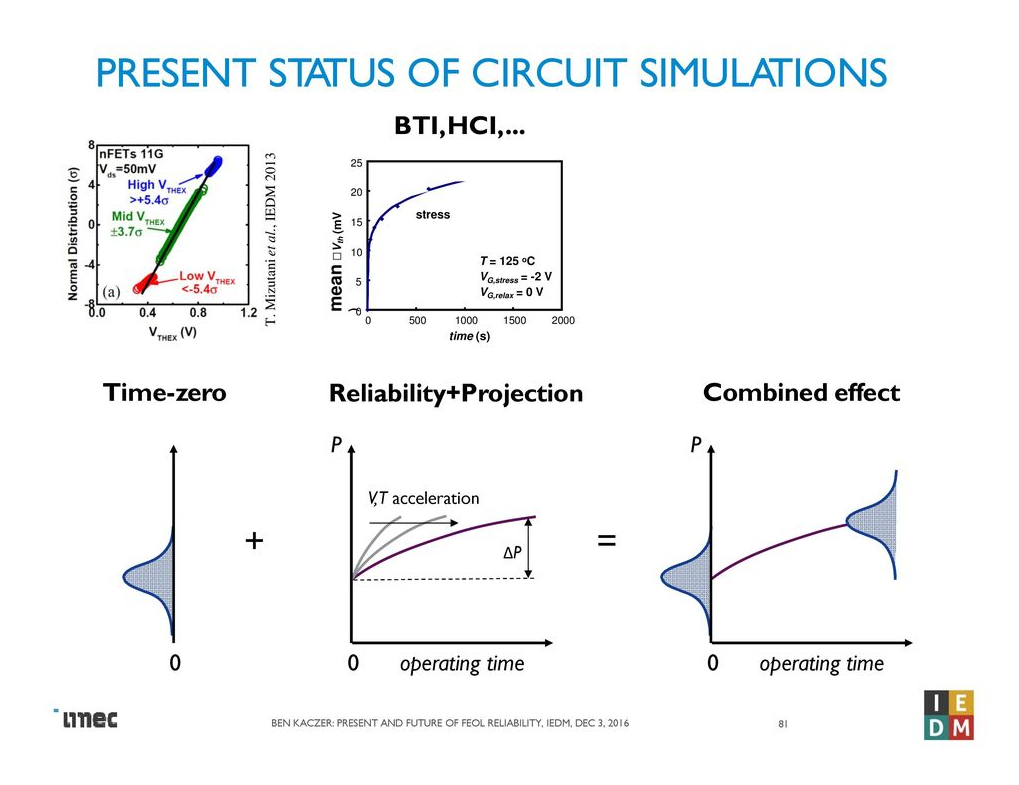
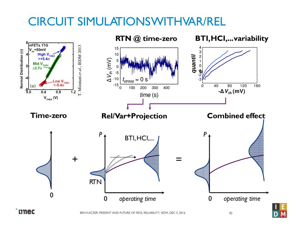
Circuit Simulations
Burn-in & High-temperature operating life (HTOL)
- HTOL:
- characterization test
- characterize the life expectancy
- Burn-in:
- production test
- weed out defective products
HTOL and Burn-in Testing capture the two ends of the reliability characterization graph known as the "bathtub curve"
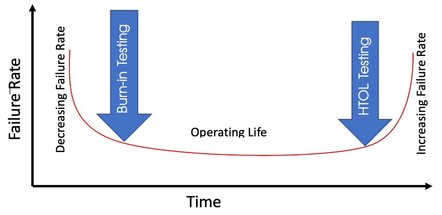
[https://arworld.us/the-importance-of-htol-and-burn-in-testing-methods/]
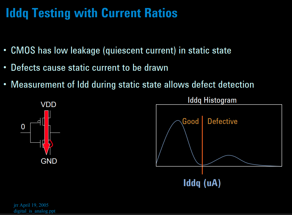
Iddq Testing
Jeff Rearick. Analog Adventures in Digital Chip Testing [https://ewh.ieee.org/r5/denver/sscs/Presentations/2005_04_Rearick.pdf]
reference
Phillip Allen. Reliability of Analog Circuits [https://aicdesign.org/wp-content/uploads/2021/04/Reliability_Theory210224-1.pdf]
M. A. Alam. ECE 695A Reliability Physics of Nanotransistors [https://nanohub.org/groups/ece695alam]
Dennis Eaton Agilent Technologies 2005. Integrated Circuit Intrinsic Reliability [https://ewh.ieee.org/r5/denver/sscs/Presentations/2005_02_Eaton.pdf]
Tanya Nigam and Andreas Kerber. Global Foundaries. CICC2014 Session 15 - Challenges for Analog Nanoscale Technologies: Reliability challenges and modeling of HK MG Technologies
Spectre Tech Tips: Device Aging? Yes, even Silicon wears out - Analog/Custom Design (Analog/Custom design) - Cadence Blogs - Cadence Community https://shar.es/afd31p
S. Liao, C. Huang, and A. C. J. X. T. Guo, "New Generation Reliability Model," Dec 2016. [Online]. Available: http://www.mos-ak.org/berkeley_2016/publications/T11_Xie_MOS-AK_Berkeley_2016.pdf. [Accessed Aug 2018]
Tianlei Guo, Jushan Xie, "A Complete Reliability Solution: Reliability Modeling, Applications, and Integration in Analog Design Environment" [https://mos-ak.org/beijing_2018/presentations/Tianlei_Guo_MOS-AK_Beijing_2018.pdf]
FinFET Reliability Analysis with Device Self-Heating via @DanielNenni https://semiwiki.com/eda/synopsys/5085-finfet-reliability-analysis-with-device-self-heating/
Chris Changze Liu 刘长泽,Hisilicon, Huawei, "Reliability Challenges in Advanced Technology Node" https://www.tek.com.cn/sites/default/files/2018-09/reliability-challenges-in-advanced-technology-node.pdf
Ben Kaczer, imec. FEOL reliability: from essentials to advanced and emerging devices and circuits. 2016 IRPS Tutorial
Ben Kaczer, imec. Present and Future of FEOL Reliability—from Dielectric Trap Properties to Reliable Circuit Operation. 2016 IEDM 2016 [link]
Kang, Sung-Mo Steve, Yusuf Leblebici and Chulwoo Kim. “CMOS Digital Integrated Circuits: Analysis & Design, 4th Edition.” (2014).
Behzad Razavi. "Design of Analog CMOS Integrated Circuits" (2016)
Basel Halak. Ageing of Integrated Circuits : Causes, Effects and Mitigation Techniques. Cham, Switzerland: Springer, 2020.
Elie Maricau, and Georges Gielen. Analog IC Reliability in Nanometer CMOS. Springer Science & Business Media, 2013.
Transistor Aging Intensifies At 10/7nm And Below https://semiengineering.com/transistor-aging-intensifies-10nm/
Modeling Effects of Dynamic BTI Degradation on Analog and Mixed-Signal CMOS Circuits. MOS-AK/GSA Workshop, April 11-12, 2013, Munich https://www.mos-ak.org/munich_2013/presentations/05_Leonhard_Heiss_MOS-AK_Munich_2013.pdf
Challenges and Solutions in Modeling and Simulation of Device Self-heating, Reliability Aging and Statistical Variability Effects https://www.mos-ak.org/beijing_2018/presentations/Dehuang_Wu_MOS-AK_Beijing_2018.pdf
New Generation Reliability Model https://www.mos-ak.org/berkeley_2016/publications/T11_Xie_MOS-AK_Berkeley_2016.pdf
FinFET SPICE Modeling: Synopsys Solutions to Simulation Challenges of Advanced Technology Nodes https://www.mos-ak.org/washington_dc_2015/presentations/T03_Joddy_Wang_MOS-AK_Washington_DC_2015.pdf
A. Zhang et al., "Reliability variability simulation methodology for IC design: An EDA perspective," 2015 IEEE International Electron Devices Meeting (IEDM), Washington, DC, USA, 2015, pp. 11.5.1-11.5.4, doi: 10.1109/IEDM.2015.7409677.
W. -K. Lee et al., "Unifying self-heating and aging simulations with TMI2," 2014 International Conference on Simulation of Semiconductor Processes and Devices (SISPAD), Yokohama, Japan, 2014, pp. 333-336, doi: 10.1109/SISPAD.2014.6931631.
Aging and Self-Heating in FinFETs - Breakfast Bytes - Cadence Blogs - Cadence Community https://community.cadence.com/cadence_blogs_8/b/breakfast-bytes/posts/aging-and-self-heating
Article (20482350) Title: Measure the Impact of Aging in Spectre Technology
Karimi, Naghmeh, Thorben Moos and Amir Moradi. “Exploring the Effect of Device Aging on Static Power Analysis Attacks.” IACR Trans. Cryptogr. Hardw. Embed. Syst. 2019 (2019): 233-256.[link]
Self-Heating Issues Spread https://semiengineering.com/self-heating-issues-spread/
Y. Zhao and Y. Qu, "Impact of Self-Heating Effect on Transistor Characterization and Reliability Issues in Sub-10 nm Technology Nodes," in IEEE Journal of the Electron Devices Society, vol. 7, pp. 829-836, 2019 [https://sci-hub.se/10.1109/JEDS.2019.2911085]