Circuit insight
Gain-boosted cascode
TODO 📅
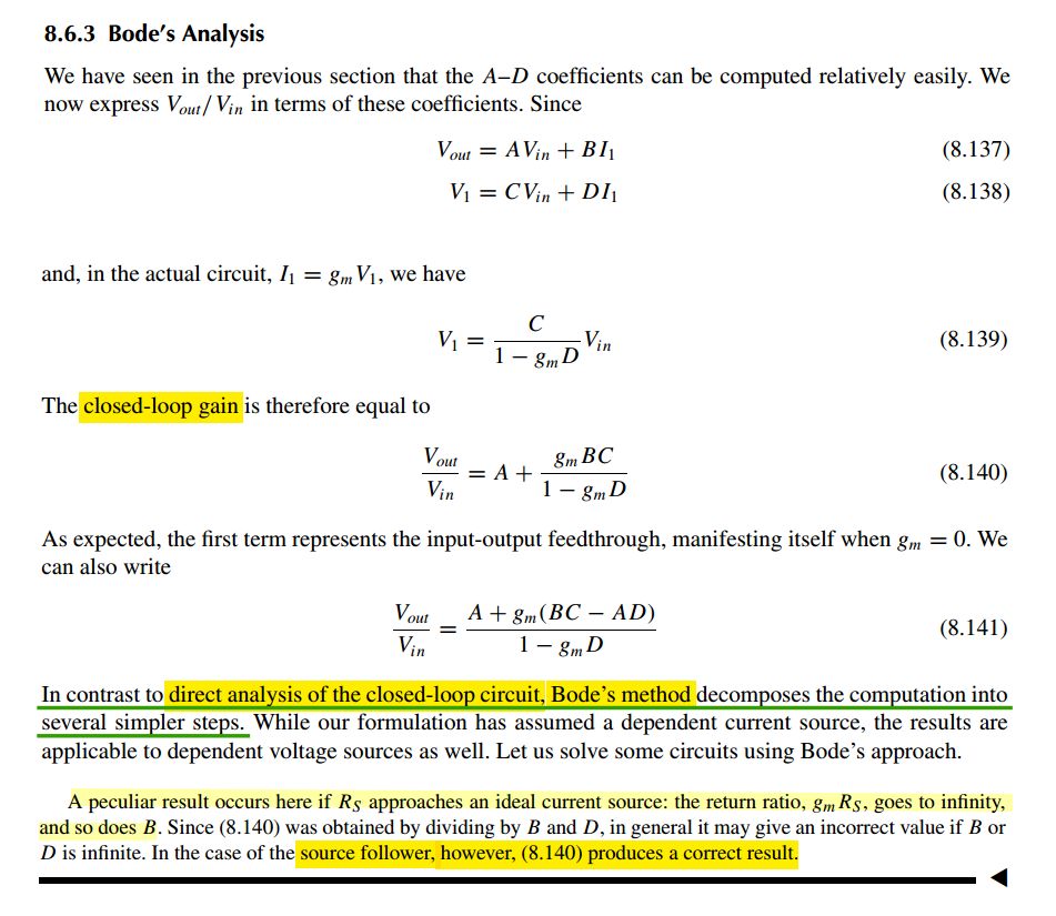
Bode's Analysis
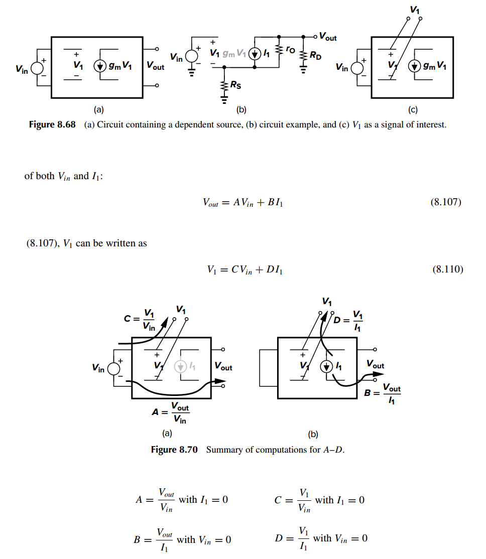
Note that ABCD here does not denote the transmission matrix of a two-port network
total sigma and correlation
\[ \sigma_{X+Y} = \sqrt{\sigma_{X}^2 + \sigma_{Y}^2 + 2\rho\sigma_{X}\sigma_{Y}} \]
\(\rho\): Pearson correlation coefficient between \(X\) and \(Y\) (ranges from \(-1\) to \(1\))
\(\rho\sigma_{X}\sigma_{Y}\): Covariance between \(X\) and \(Y\)
Perfect Positive Correlation \(\rho = 1\): the variables move exactly together, \(\sigma_{total} = \sigma_{X} + \sigma_{Y}\)
Zero Correlation \(\rho = 0\): the geometric sum of individual variations, \(\sigma_{total} = \sqrt{\sigma_{X}^2 + \sigma_{Y}^2}\)
Perfect Negative Correlation \(\rho = -1\): variables offset each other's fluctuations, \(\sigma_{total} = \vert{}\sigma_X - \sigma_Y\vert{}\)
Zero-Value Time Constant Analysis
TODO 📅
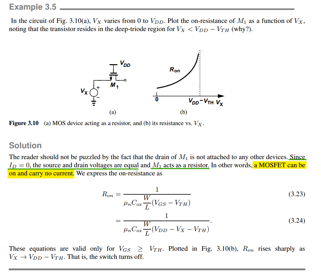
MOS as resistor
MOSFET can be on and carry no current
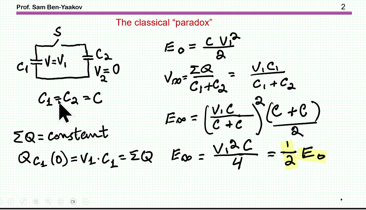
Two capacitor paradox
Intuitive examination of the two-capacitors "paradox"l [https://youtu.be/WNpxV5qAUMU]
The two-capacitor paradox is a classic puzzle in circuit theory where energy seems to vanish
If there is any resistance $R $ (always true in reality). $R $ dissipates heat
If the resistance is genuinely zero, Then you can't ignore inductance — With pure $LC $, the circuit becomes an oscillator
Two capacitors \(C\) in series around the loop give an effective capacitance \(C_{eq} = C/2\). With inductance \(L\) in the loop, the resonant frequency is \[ \omega_0 = \frac{1}{\sqrt{LC_{eq}}} = \frac{1}{\sqrt{L(C/2)}} = \sqrt{\frac{2}{LC}} \]
.png) \[
v_1(t) = \frac{V_0}{2}\left(1 + \cos\omega_0 t\right), \qquad
v_2(t) = \frac{V_0}{2}\left(1 - \cos\omega_0 t\right)
\] the \(y\)-axis is in units of
\(V_0\), so the curves run between 0
and 1 \[
v_1(t) + v_2(t) = V_0 \quad \text{at all times}
\]
\[
v_1(t) = \frac{V_0}{2}\left(1 + \cos\omega_0 t\right), \qquad
v_2(t) = \frac{V_0}{2}\left(1 - \cos\omega_0 t\right)
\] the \(y\)-axis is in units of
\(V_0\), so the curves run between 0
and 1 \[
v_1(t) + v_2(t) = V_0 \quad \text{at all times}
\]
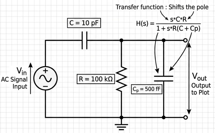
RC High-Pass Filter (R in parallel with \(C_p\))
1 | import numpy as np |
Transmission Gate
Equivalent Resistance is defined by large signal
[https://www.ece.ucdavis.edu/~ramirtha/EEC116/F11/TGlecture.pdf]
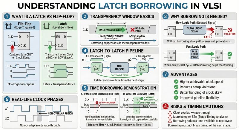
latch borrowed time
Kunal Saraswat [link]
Digital DC Offset Correction
 \[
X- Y\cdot \beta z^{-1}\cdot \frac{1}{1-z^{-1}} = Y
\] therefore \[
\frac{Y}{X} = \frac{1-z^{-1}}{1-(1-\beta)z^{-1}}
\]
\[
X- Y\cdot \beta z^{-1}\cdot \frac{1}{1-z^{-1}} = Y
\] therefore \[
\frac{Y}{X} = \frac{1-z^{-1}}{1-(1-\beta)z^{-1}}
\]
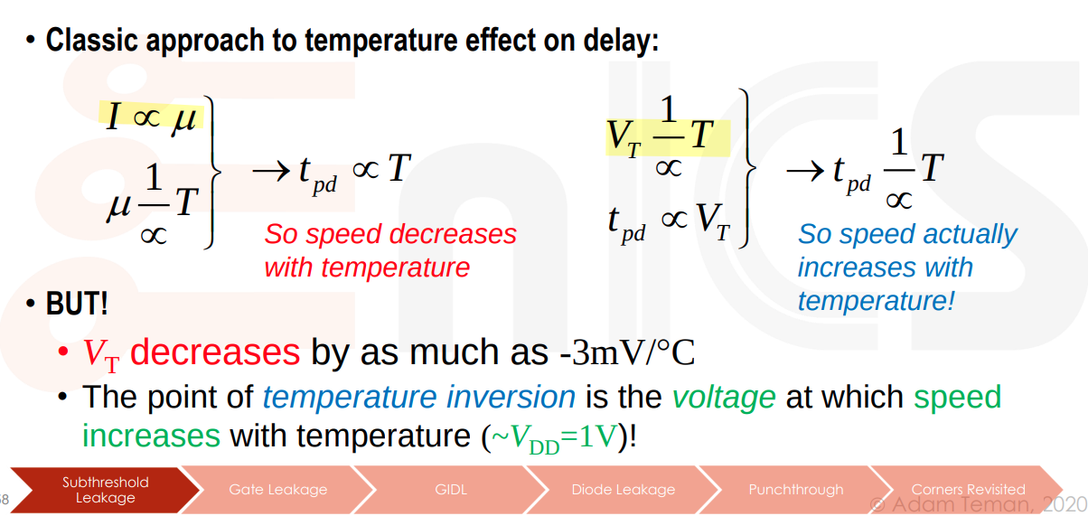
Temperature Inversion
Adam Teman. Digital Integrated Circuits (83-313) Lecture 3: MOSFET Modeling [pdf]
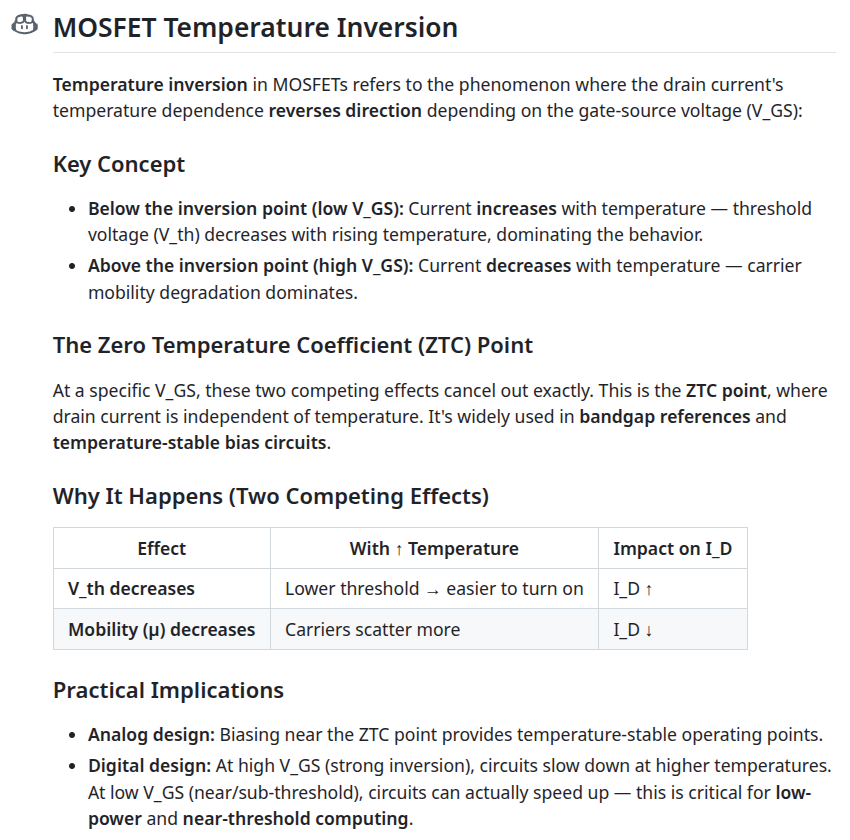
Zero Temperature Coefficient (ZTC) Bias Points
M. Coelho et al., "Is There a ZTC Biasing Point in the Leading-Edge FET Intrinsic Gain gmrDS?," 2025 9th International Young Engineers Forum on Electrical and Computer Engineering (YEF-ECE), Caparica / Lisbon, Portugal, 2025
M. Coelho et al., "Analysis of the ZTC Bias Points in the FinFET Gate Capacitance and Transition Frequency," 2025 37th International Conference on Microelectronics (ICM), Cairo, Egypt, 2025, pp. 1-6, doi: 10.1109/ICM66518.2025.11322461
there's a specific bias point where the MOSFET transition frequency (fT) becomes almost temperature‑independent
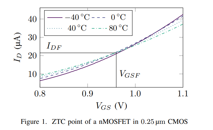
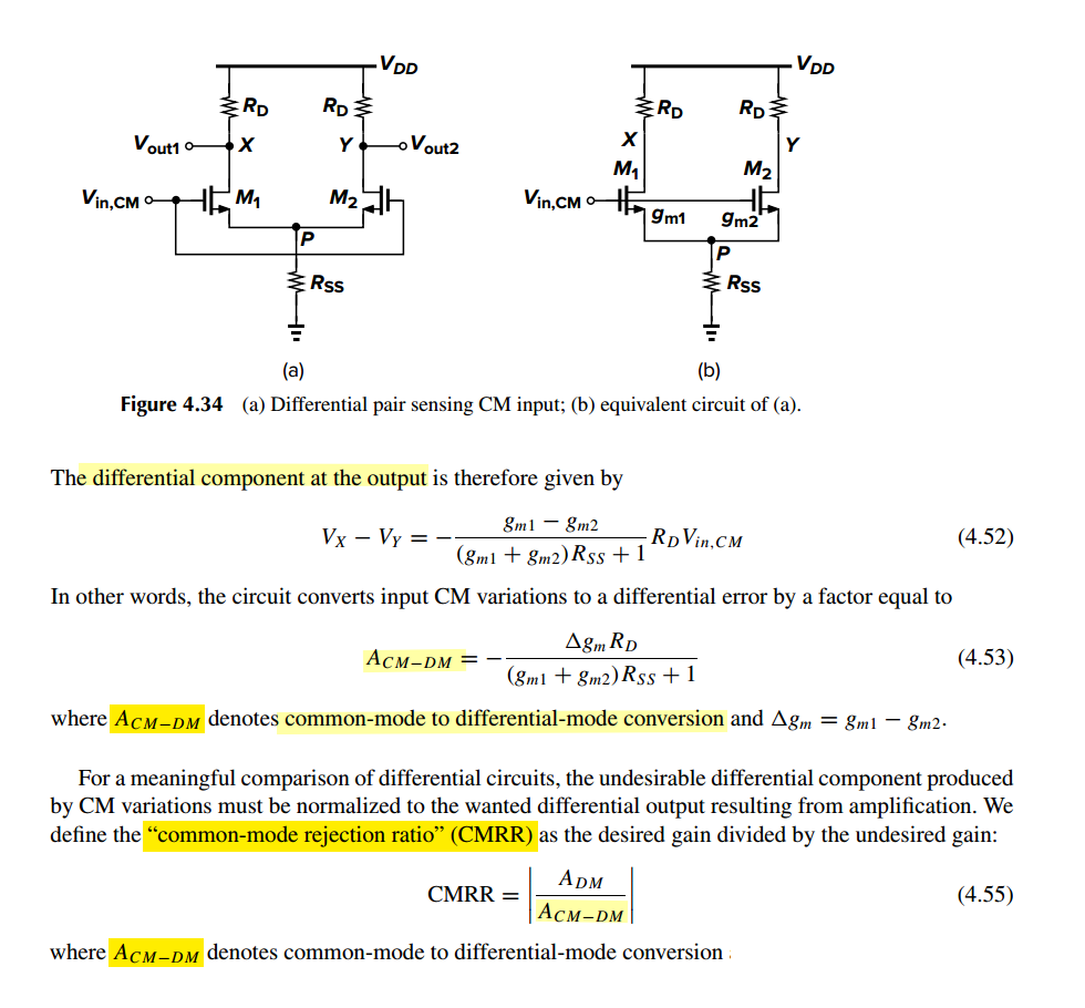
CMRR (Common-Mode Properties)
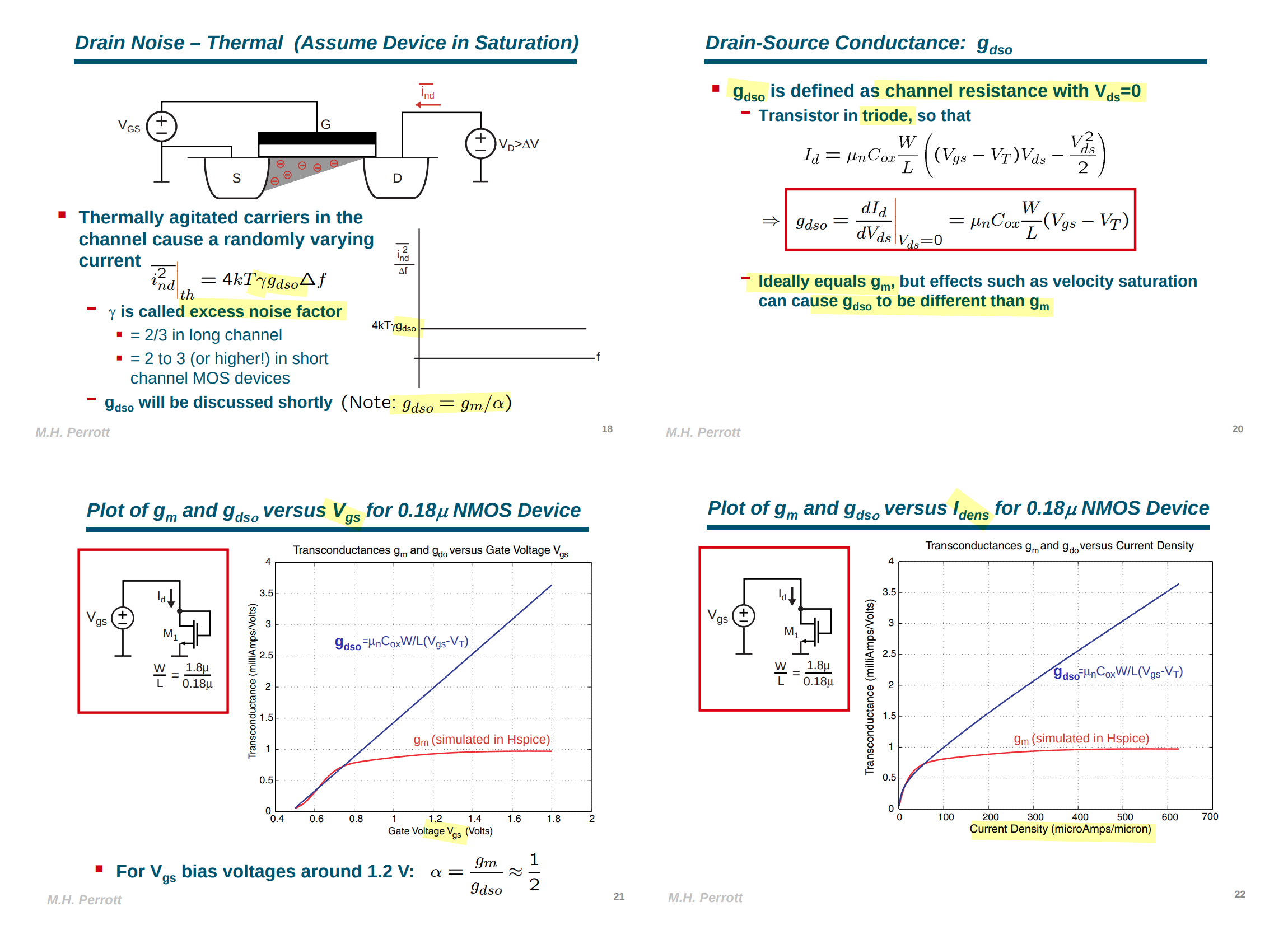
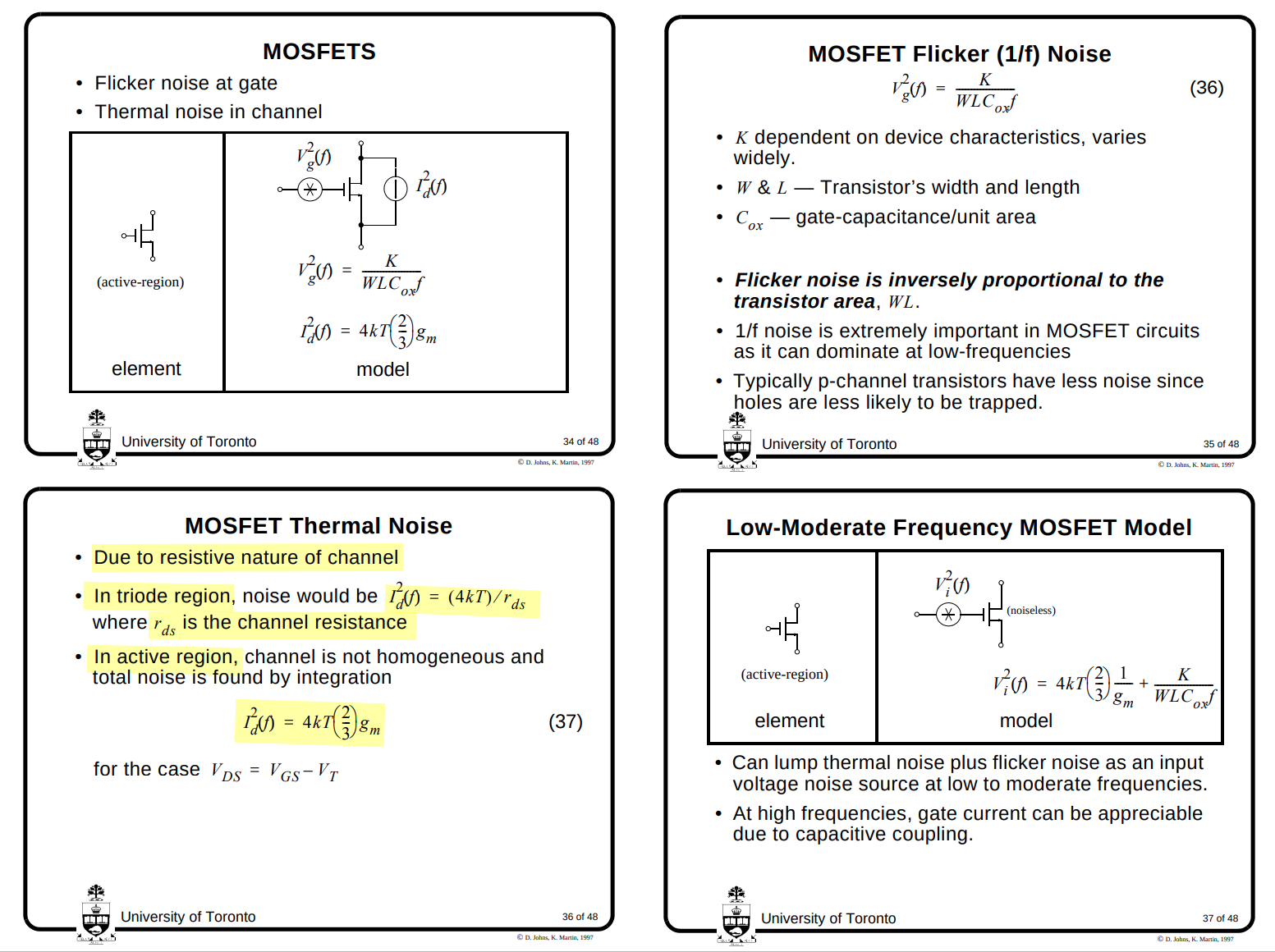
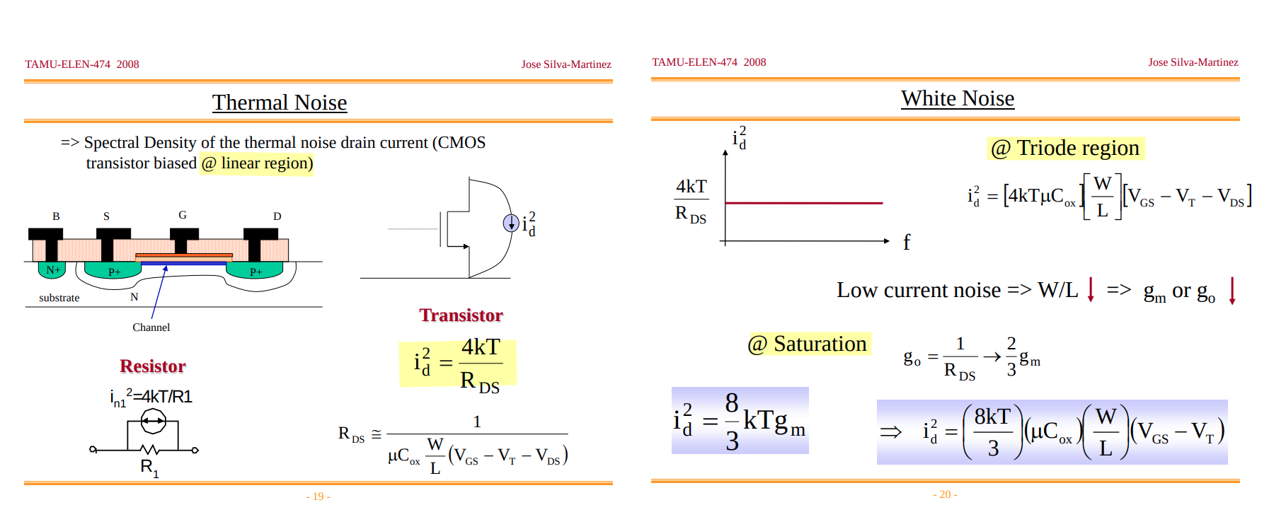
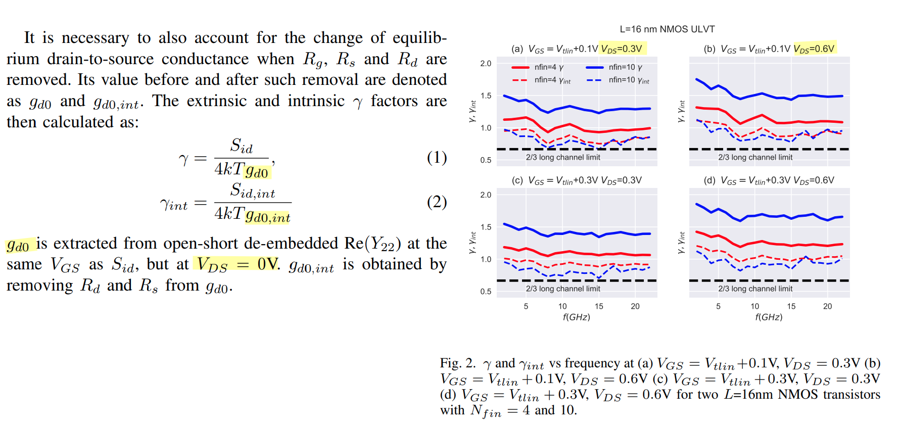
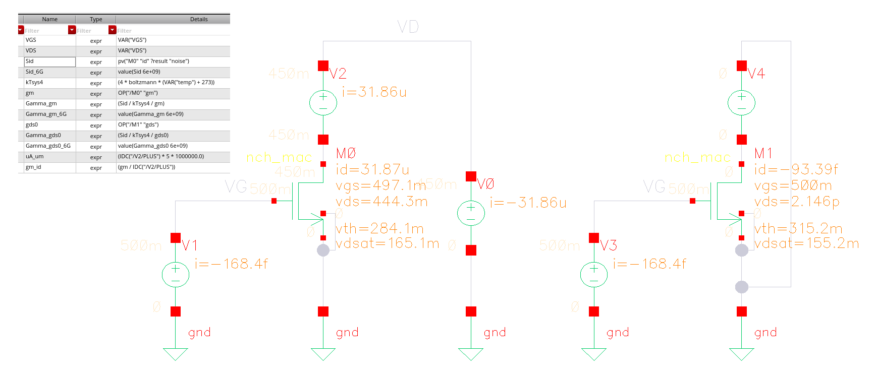
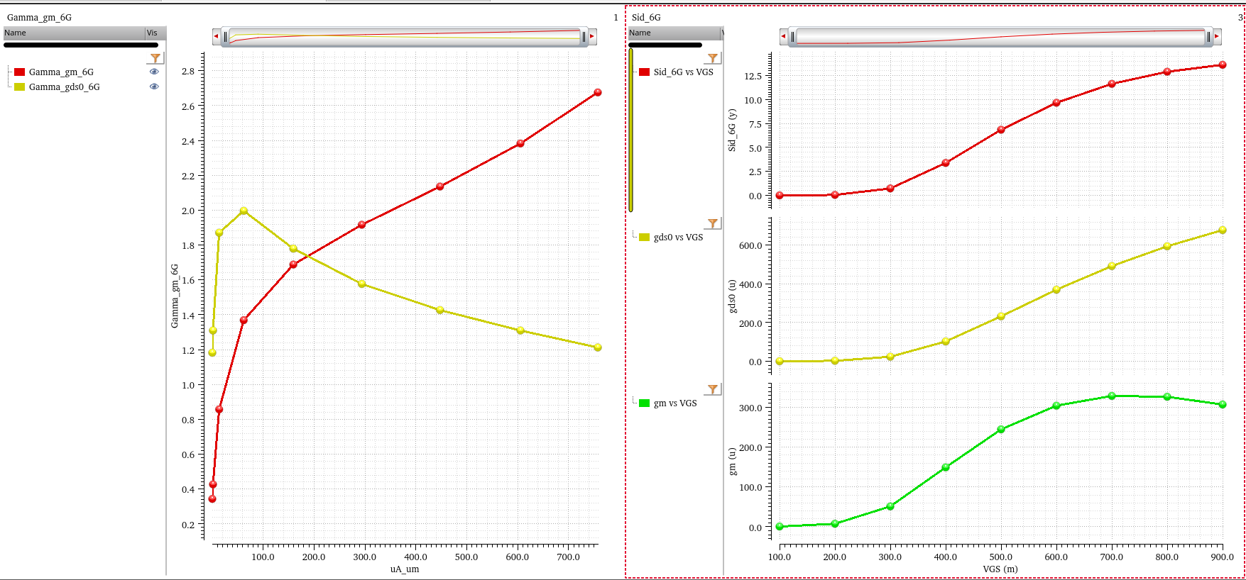
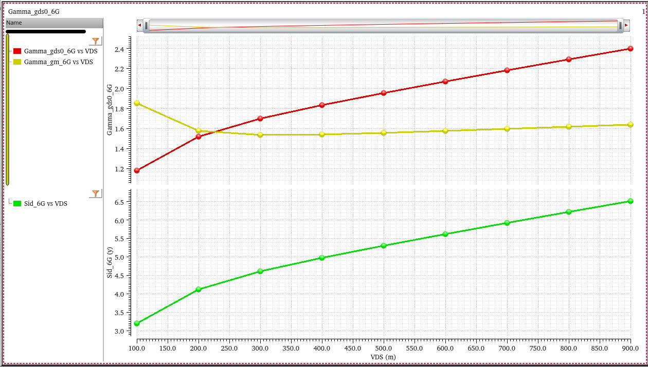
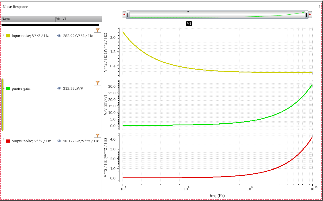
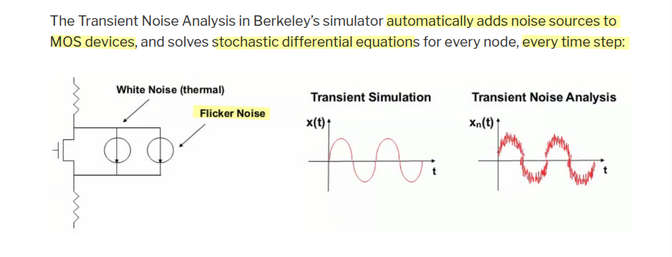
MOS Noise
MOS Thermal Noise
Michael H. Perrott. Analysis and Design of Analog Integrated Circuits Lecture 14 Noise Spectral Analysis for Circuit Elements [https://www.cppsim.com/CircuitLectures/Lecture14.pdf]
Legacy Long-Channel Model
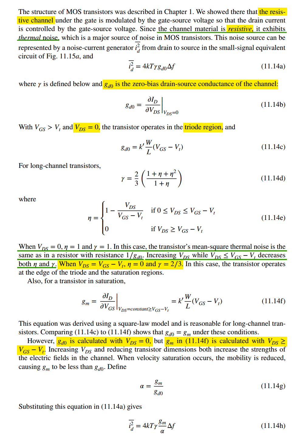 \[
\color{red} \overline{i^2_d} \propto \gamma \propto \eta \propto
\frac{1}{V_{DS}}
\]
\[
\color{red} \overline{i^2_d} \propto \gamma \propto \eta \propto
\frac{1}{V_{DS}}
\]
[https://www.eecg.toronto.edu/~johns/ece512/lecture_notes/04_noise_2_per_page.pdf]
[https://people.engr.tamu.edu/spalermo/ecen474/lecture12_ee474_noise.pdf]
Short-Channel Effects
Gildenblat, G. S. (2010). Compact modeling : principles, techniques and applications. Springer.
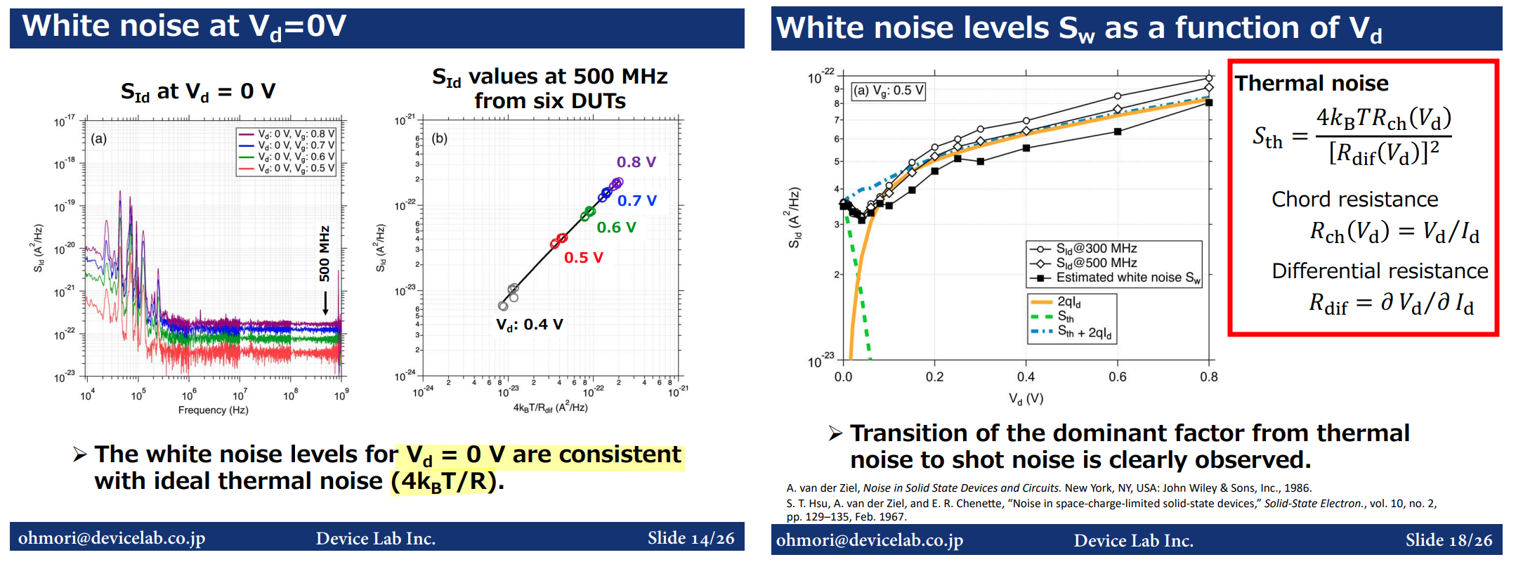
VDS Effect On Channel Noise
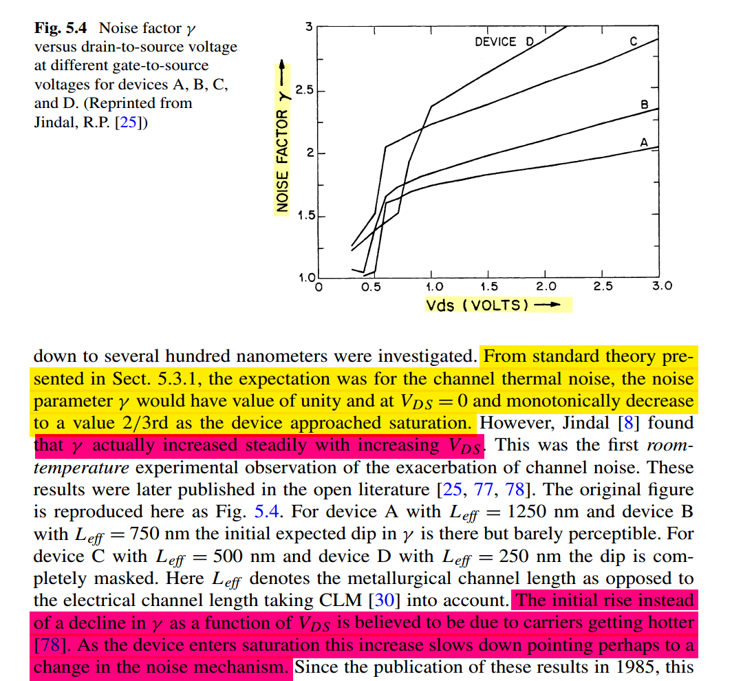
\[
\color{red} \overline{i^2_d} \propto V_{DS}
\] 
K. Ohmori and S. Amakawa, "Direct White Noise Characterization of Short-Channel MOSFETs," in IEEE Transactions on Electron Devices, vol. 68, no. 4, pp. 1478-1482, April 2021 [pdf, slides]
X. Ding, G. Niu, A. Zhang, W. Cai and K. Imura, "Experimental Extraction of Thermal Noise γ Factors in a 14-nm RF FinFET technology," 2021 IEEE 20th Topical Meeting on Silicon Monolithic Integrated Circuits in RF Systems (SiRF), San Diego, CA, USA, 2021[https://sci-hub.se/10.1109/SiRF51851.2021.9383331]
NF50
TODO 📅
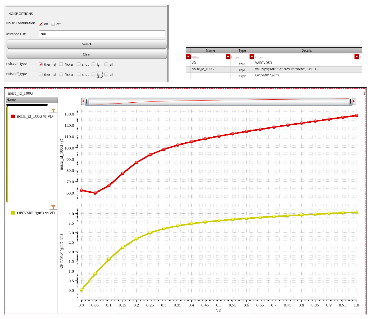
\(\gamma\) vs VDS, VGS in simulation
N28
fix VDS, sweep VGS
fix VGS, sweep VDS
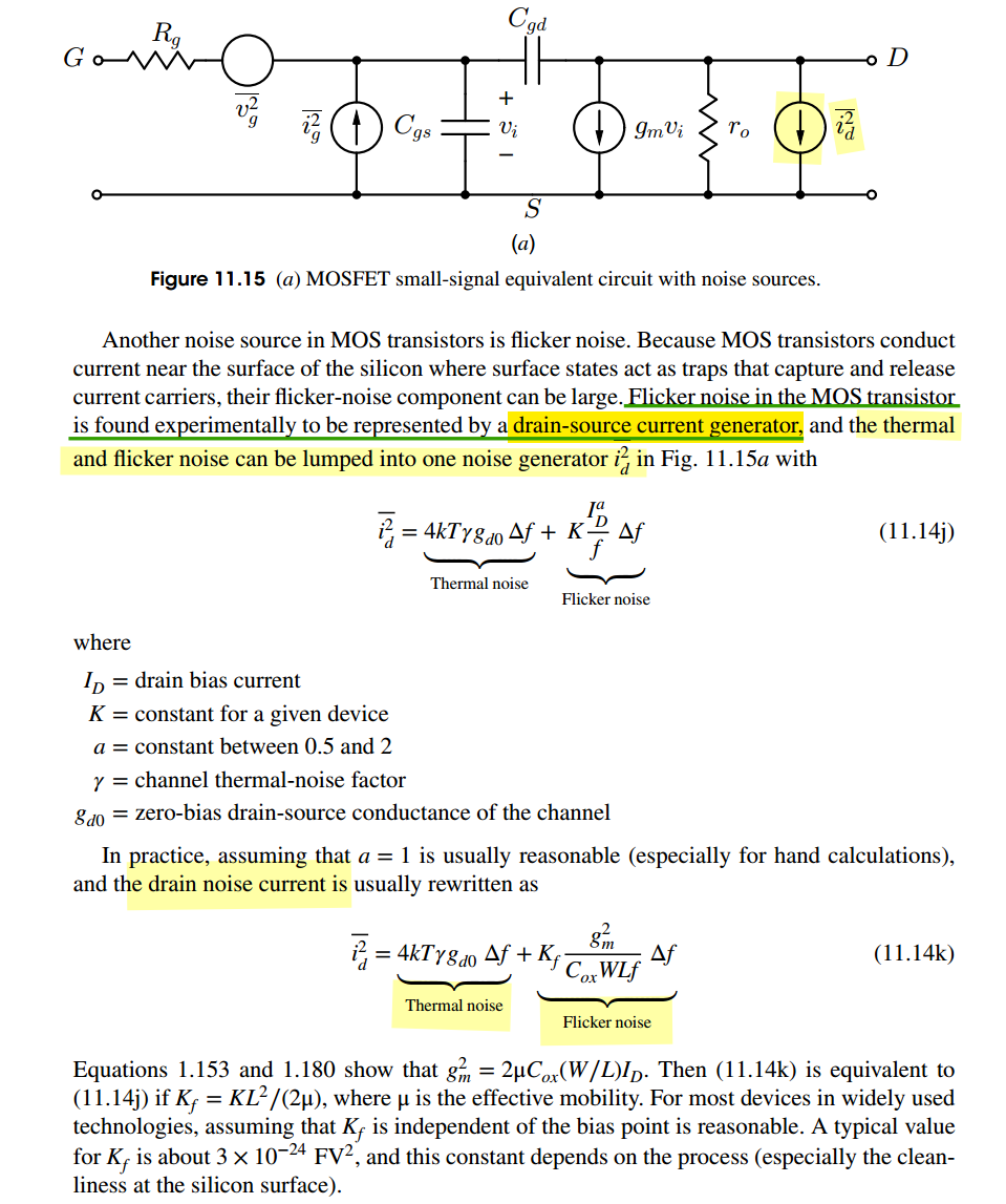
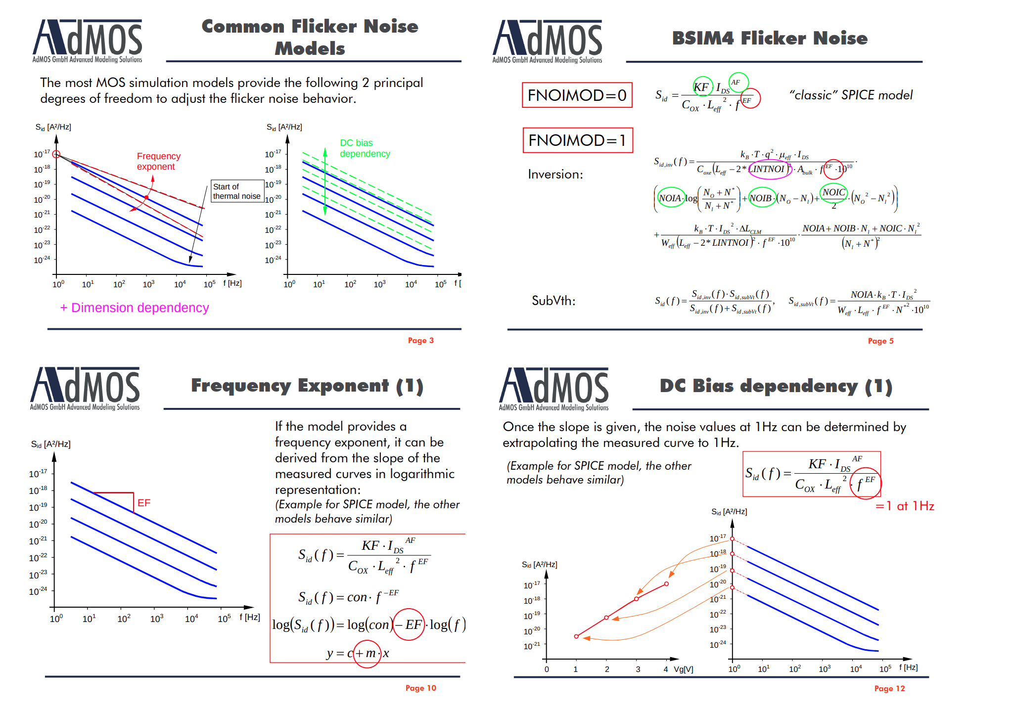
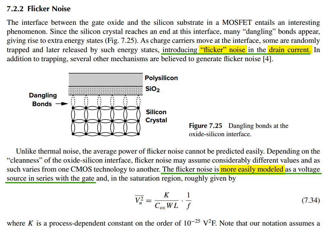
MOS Flicker Noise
T. Noulis, "CMOS process transient noise simulation analysis and benchmarking," 2016 26th International Workshop on Power and Timing Modeling, Optimization and Simulation (PATMOS), Bremen, Germany, 2016 [https://sci-hub.ru/10.1109/PATMOS.2016.7833428]
Dr. Thomas Gneiting, AdMOS GmbH. Flicker Noise Extraction for Scalable MOS Simulation Models [https://www.mos-ak.org/premstaetten/papers/MOS-AK_T.Gneiting.pdf]
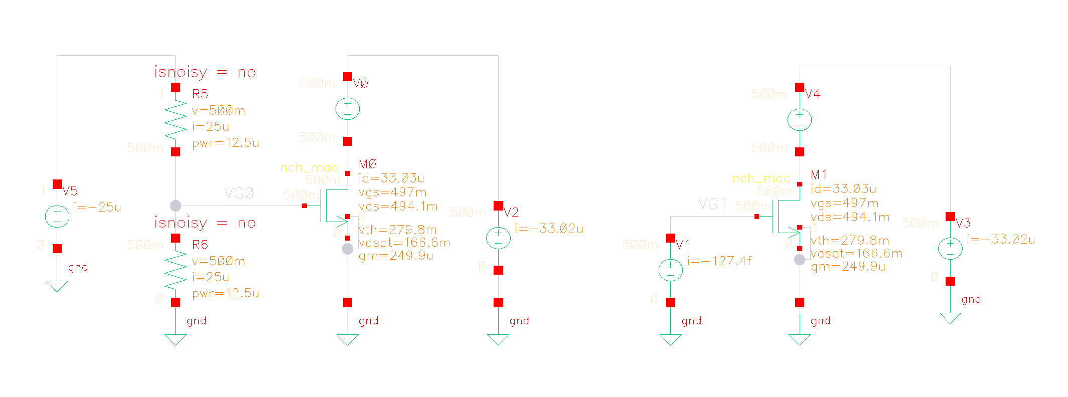
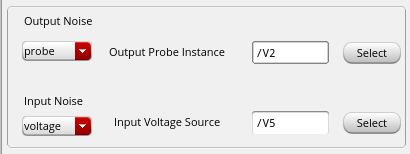
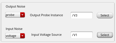
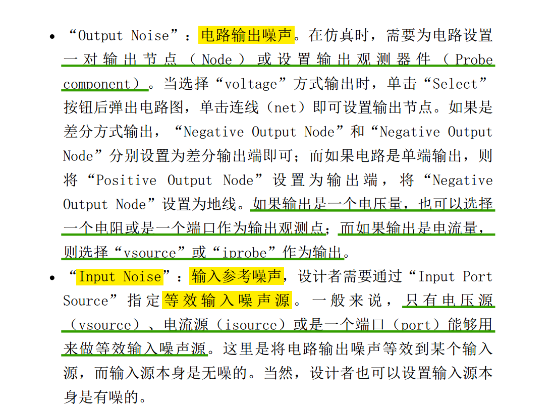
| Noise analysis ON,IN cfg | input noise, noise gain, output noise | |
|---|---|---|
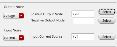 |
 |
i: Id o: Vg |
 |
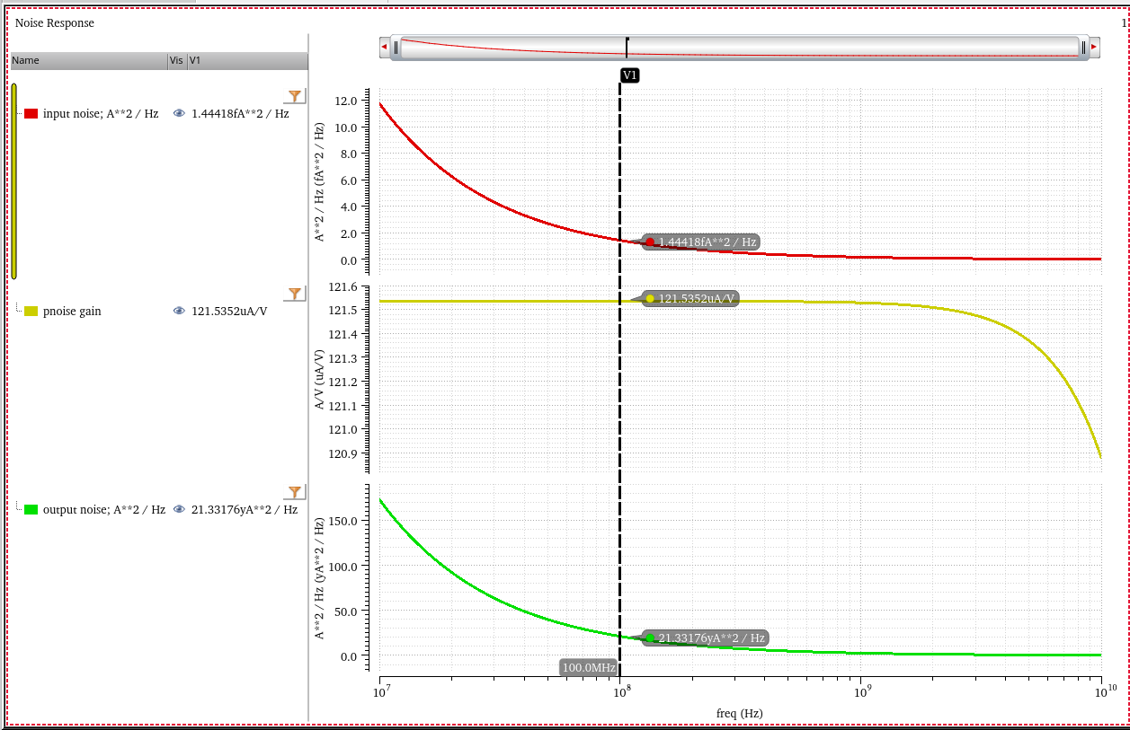 |
i: V5 o: Id |
 |
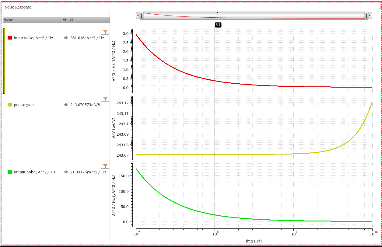 |
i: V1 o: Id |
Above simulation demonstrate that flicker noise is represented by a drain-source current in BSIM model, however modeled as a voltage source in series with the gate is just for calculating convenience
David Lee, Berkeley DA. Device Noise Analysis of Switched-Cap Circuits [https://semiwiki.com/eda/2900-device-noise-analysis-of-switched-cap-circuits/]
Sam Palermo. Lecture 12: Noise. ECEN474: (Analog) VLSI Circuit Design Fall 2012 [https://people.engr.tamu.edu/spalermo/ecen474/lecture12_ee474_noise.pdf]
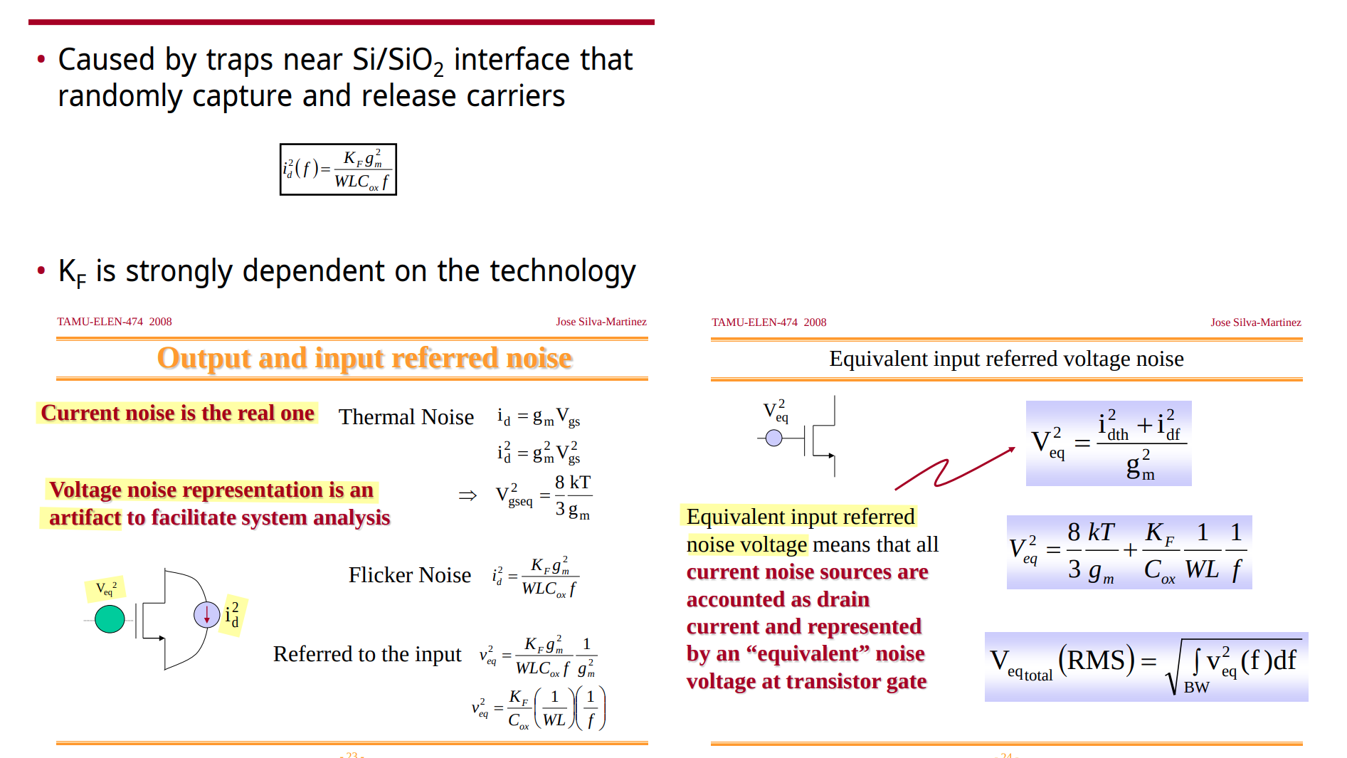
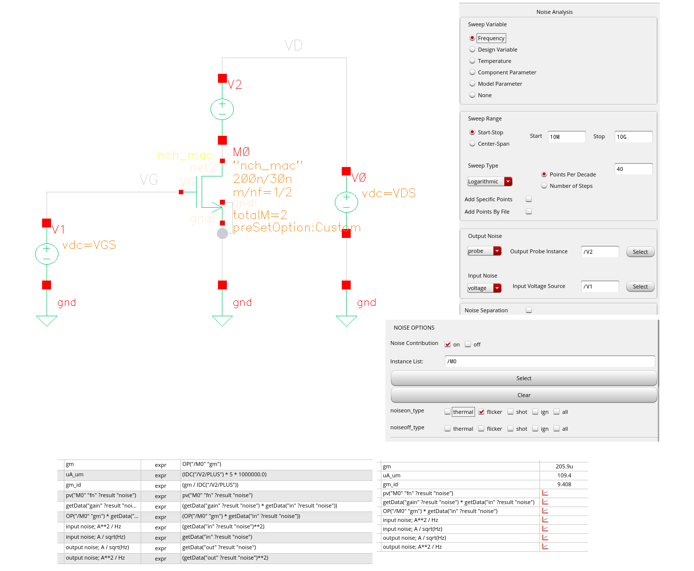
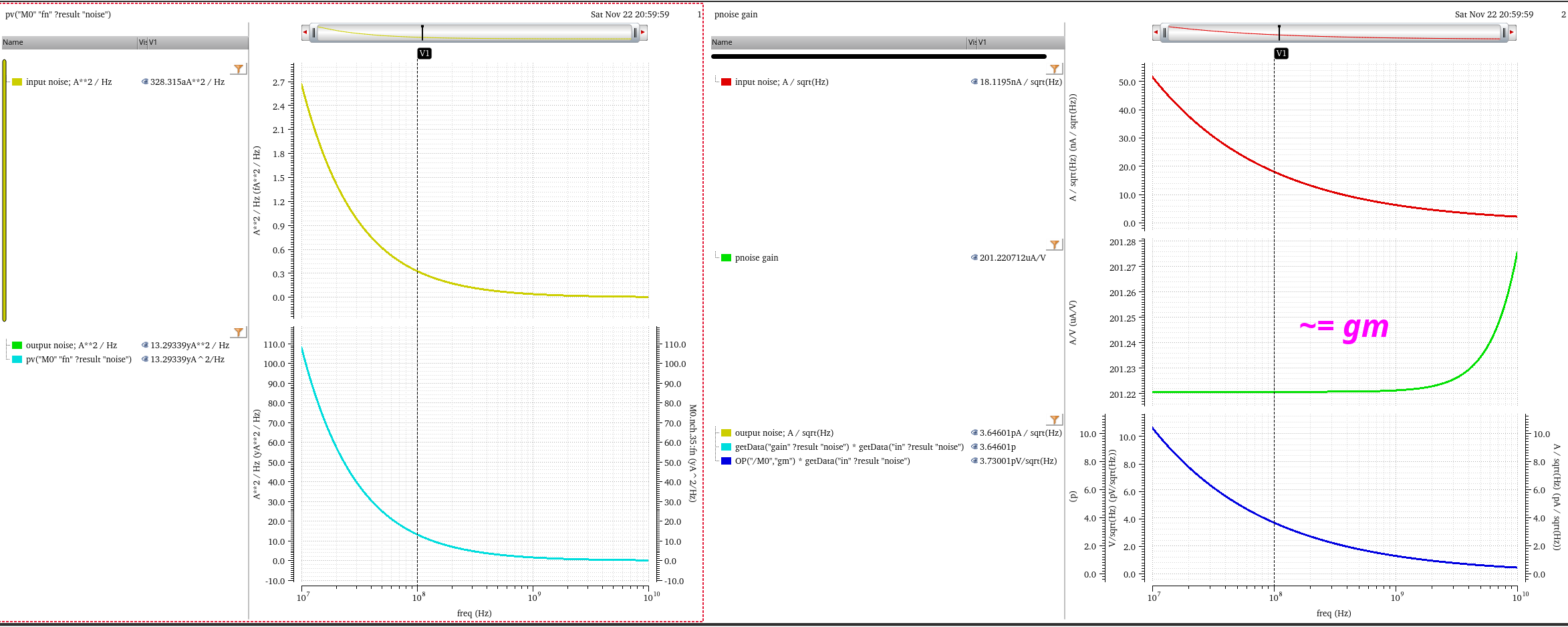
Notice, input referred noise unit follow output noise's unit
陈铖颖,杨丽琼,王统. CMOS模拟集成电路设计与仿真实例:基于CadenceADE. 电子工业出版社,2013
Ma, Mb are parallel MOS, with width \(W_a\) and \(W_b\), Since flicker noise current \(\overline{I_{D}^2}(\Delta f) = K_f\frac{g_{m}^2}{C_{ox}WL}\frac{\Delta f}{f}\) and \(g_{m,tot}=g_{m,a} + g_{m,b}\), \(W_{tot} = W_a + W_b\), \(g_{m,a} = \beta W_a\), \(g_{m,b}=\beta W_b\) \[ \overline{I_{D,a}^2}(f) =K_f\frac{\beta^2W_a}{C_{ox}L}\frac{\Delta f}{f} \quad \overline{I_{D,b}^2}(f) = K_f\frac{\beta^2W_b}{C_{ox}L}\frac{\Delta f}{f} \quad \overline{I_{D,tot}^2}(f) = K_f\frac{\beta^2(W_a+W_b)}{C_{ox}L}\frac{\Delta f}{f} \\ \]
Then \[ \color{green}\overline{I_{D,tot}^2} \equiv \overline{I_{D,a}^2} + \overline{I_{D,b}^2} \]
MOS Shot Noise
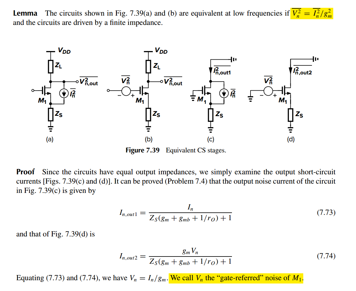
Gate-Referred Noise Lemma
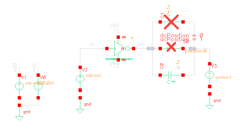
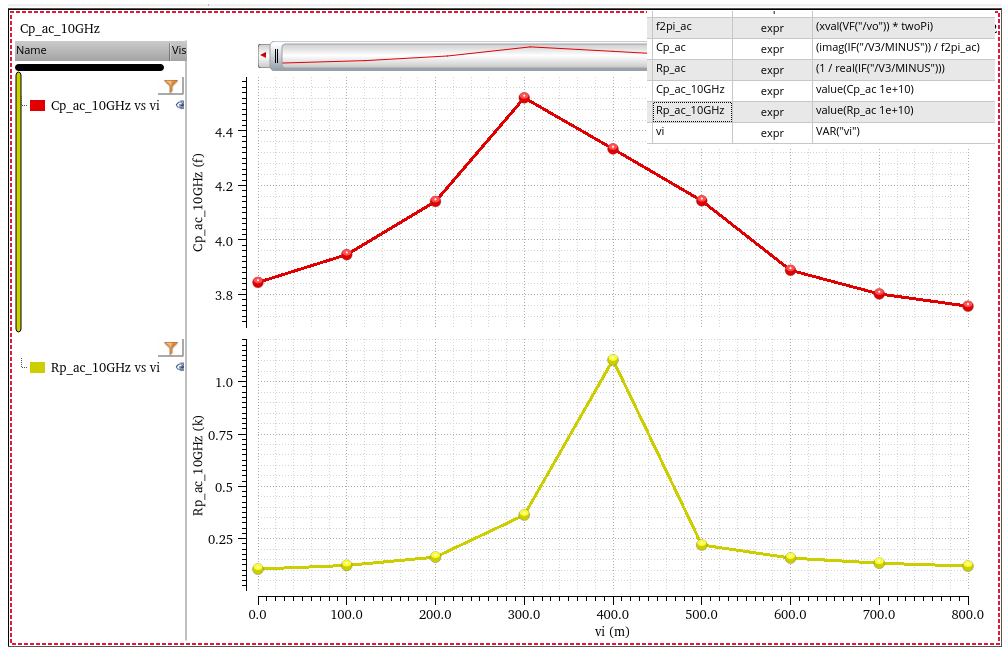
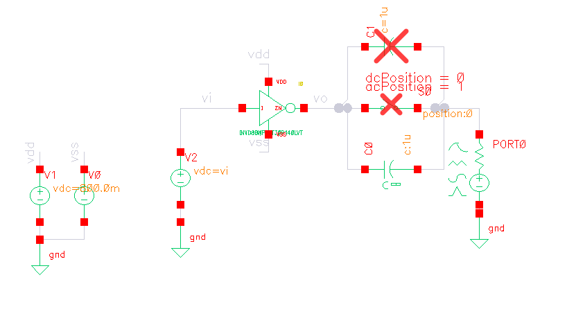
inverter capacitance simulation
inverter input
R-C, series equivalent circuit
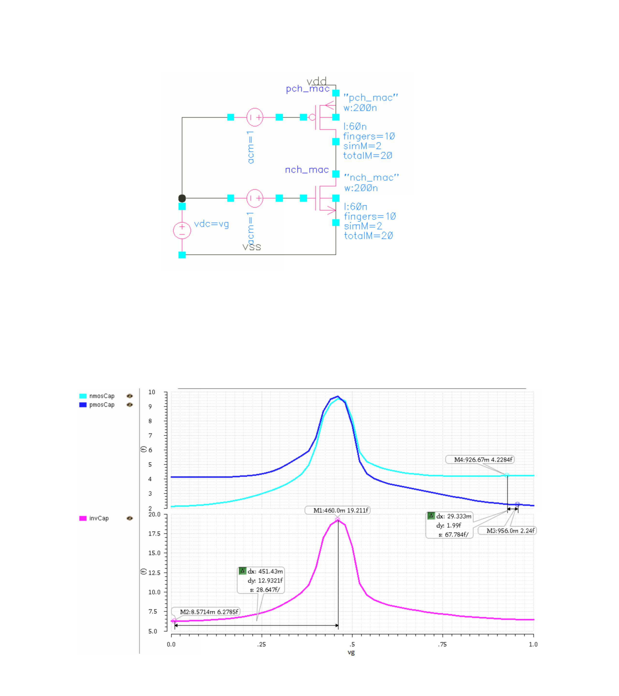
inverter output
R-C, parallel equivalent circuit
AC simulation
@vi = 0
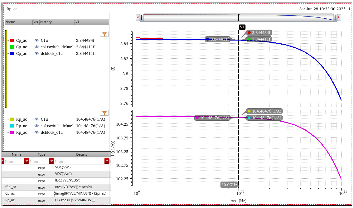
sweep vi from 0 to 800mV (vdd)
SP simulation
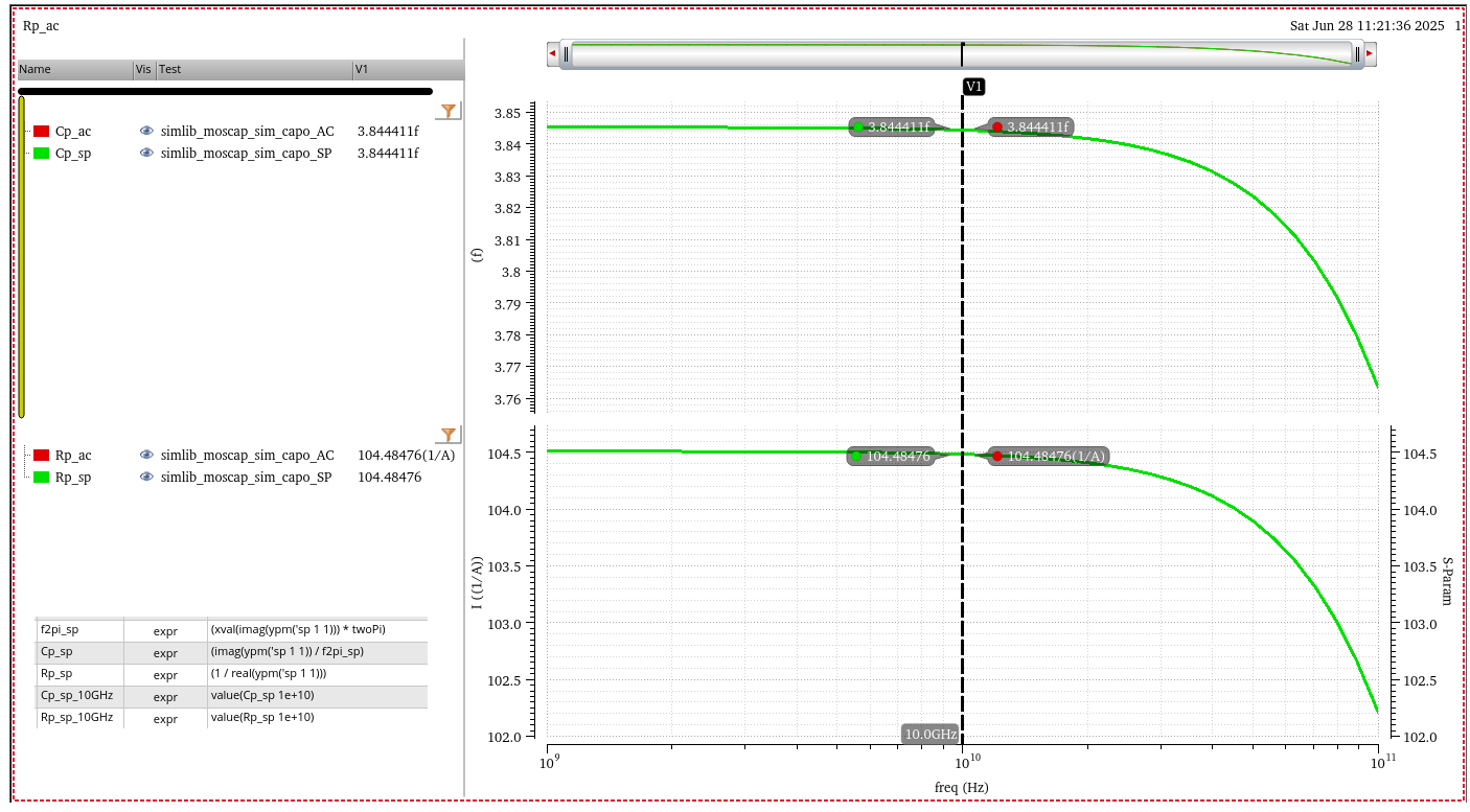
EEStream. Cadence - How to find device capacitance - DC simulation, SP simulation and Large-signal SP simulation [https://www.youtube.com/watch?v=M3zP6eJnONk]
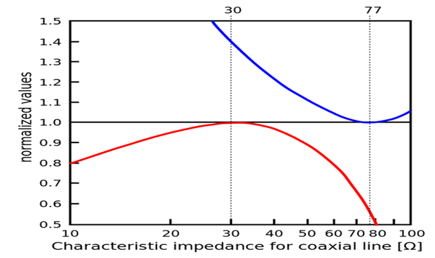
50-ohm?
Why is 50-ohm characteristic impedance standardized in RF and Microwave systems? [link]
[https://www.microwaves101.com/encyclopedias/why-fifty-ohms]
It was a compromise made and a tradeoff between power handling (red curve) and losses (blue curve)
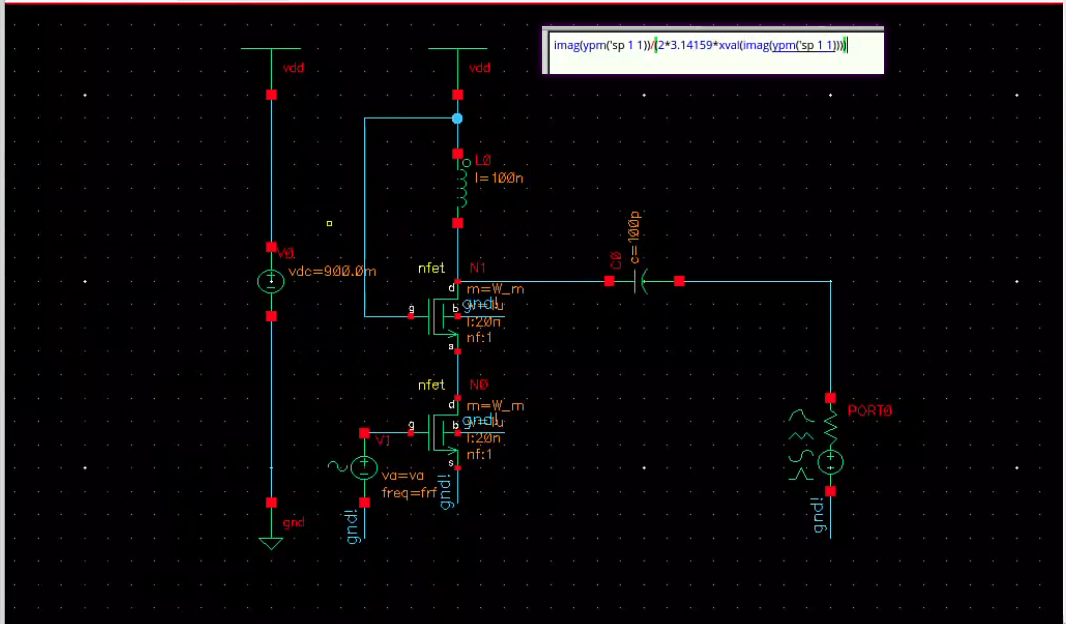
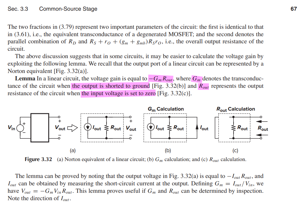
Gm Rout Lemma
\[ A_V = -G_m R_{out} \]
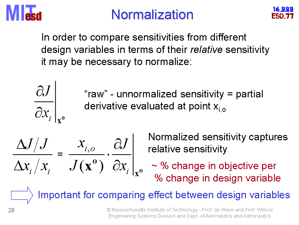
Relative Sensitivity
Olivier de Weck, Karen Willcox. MIT, Gradient Calculation and Sensitivity Analysis [pdf]
Karti Mayaram, ECE 521 Fall 2016 Analog Circuit Simulation, Sensitivity and noise analyses [https://web.engr.oregonstate.edu/~karti/ece521/lec16_11_09.pdf]
Assuming Target \(T\) ( for example, the total resistance) is function of \(x_1,x_2,...,x_N\), then total variation can be expressed as
\[\begin{align} \mathrm{d}T &= \sum_{n=1}^N\frac{\partial T}{\partial x_n}dx_n = \sum_{n=1}^N\frac{\partial T}{\partial x_n}x_n\cdot \frac{\mathrm{d}x_n}{x_n} \end{align}\]
Then, we obtain relative variation \[\begin{align} \frac{\mathrm{d}T}{T} &= \sum_{n=1}^N\frac{\partial T}{\partial x_n}\frac{x_n}{T}\cdot \frac{\mathrm{d}x_n}{x_n} = \sum_{n=1}^N S_{x_n}^T \cdot \frac{\mathrm{d}x_n}{x_n} \end{align}\]
⭐ where \(S_{x_n}^T=\frac{\partial T}{\partial x_n}\frac{x_n}{T}\) is relative sensitivity
relative sensitivity connect \(\frac{\mathrm{d}x_n}{x_n}\) with total relative variation \(\frac{\mathrm{d}T}{T}\)
And \(\mathrm{d}T\) can be expressed as \[ dT =\sum_{n=1}^N S_{x_n}^T T\cdot \frac{\mathrm{d}x_n}{x_n} = \sum_{n=1}^N x_n'\cdot \frac{\mathrm{d}x_n}{x_n} \] ⭐ where \(x_n'= S_{x_n}^T T\) is the contribution of \(x_n\) in \(T\)
⭐ For parallel or series resistors, it can prove \(\sum_{n=1}^N S_{x_n}^T = 1\) and \(\sum_{n=1}^N x_n'=T\)

Here \(T= R_1 \parallel R_2 = \frac{R_1R_2}{R_1+R_2}\), and \(T|_{R_1=8000, R_2=2000} = 1600\)
We obtain relative sensitivity: \[\begin{align} S_{R_1}^T = \frac{R_2}{R_1+R_2} \qquad S_{R_2}^T = \frac{R_1}{R_1+R_2} \end{align}\]
The contribution of \(R_1\) and \(R_2\) to \(T\) \[\begin{align} R_1' &= S_{R_1}^T T | _{R_1=8000, R_2=2000} = 320 \\ R_2' &= S_{R_2}^T T | _{R_1=8000, R_2=2000} = 1280 \end{align}\]
Normalized sensitivity captures relative sensitivity
change in objective per change in design variable
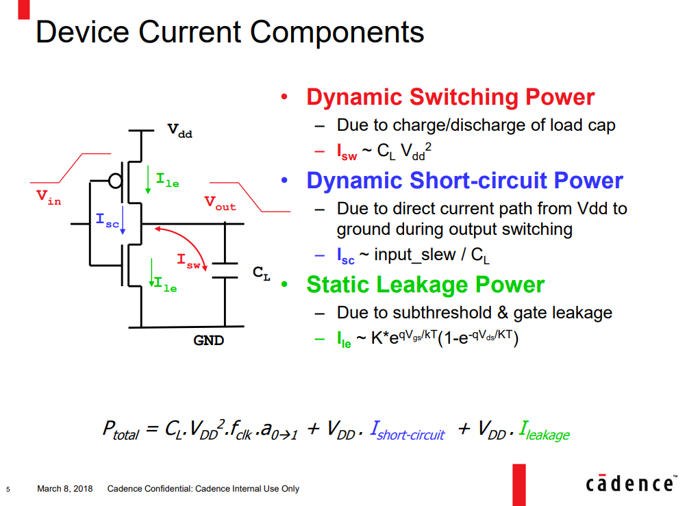
Device Current Components
common gate amplifiers
Level Shifter
TIA
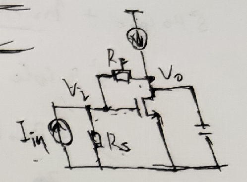
\[\begin{align} I_{in} &= \frac{V_i}{R_S} + \frac{V_i - V_o}{R_F} \\ \frac{V_i - V_o}{R_F} &= g_m V_i \end{align}\]
Then
\[\begin{align} V_o &= \frac{I_{in}R_F}{\frac{R_S+R_F}{R_S}\frac{1}{1-g_mR_F}- 1} \\ V_i &= \frac{I_{in}R_F}{\frac{R_F}{R_S}+g_mR_F} \end{align}\] If \(R_S \gg R_F\) \[\begin{align} V_o &= \frac{I_{in}}{g_m}(1-g_mR_F) \\ V_i &= \frac{I_{in}}{g_m} \end{align}\]
linearity > TIA stage allows for improved gain with better linearity, as mostly signal current passes through \(R_F\) TODO 📅 ??? Quantitative analysis
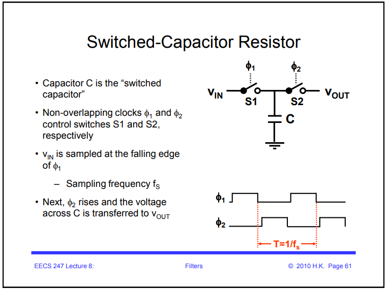
Switched-Capacitor Resistor
\[ R_{eq} = \frac{1}{f_sC} \]
Channel-Length Modulation & Pinched off
- \(\lambda \propto \frac{1}{L_g}\)
- \(\lambda \propto \frac{1}{V_{DS}}\)
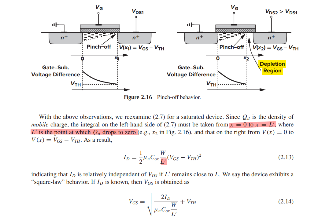
- If \(V_{DS}\) is slightly greater than \(V_{GS} - V_{TH}\), then the inversion layer stops at \(x \leq L\), and we say the channel is "pinched off"
- Upon passing the pinchoff point, the electrons simply shoot through the depletion region near the drain junction and arrive at the drain terminal
\(L^{'}\) is the function of \(V_{DS}\)
with \(\frac{1}{L^{'}} = \frac{1}{L-\Delta L}=\frac{L+\Delta L}{L^2-\Delta L^2}\approx \frac{1}{L}\left(1+\frac{\Delta L}{L}\right)\), we have \[ I_D \approx \frac{1}{2}\mu_n C_{ox}\frac{W}{L}\left(1+\frac{\Delta L}{L}\right)(V_{GS}-V_{TH})^2 = \frac{1}{2}\mu_n C_{ox}\frac{W}{L}(V_{GS}-V_{TH})^2 (1+\lambda V_{DS}) \] assuming \(\frac{\Delta L}{L} = \lambda V_{DS}\)
\(\lambda\) represents the relative variation in length for a given increment in \(V_{DS}\). Thus, for longer channels, \(\lambda\) is smaller
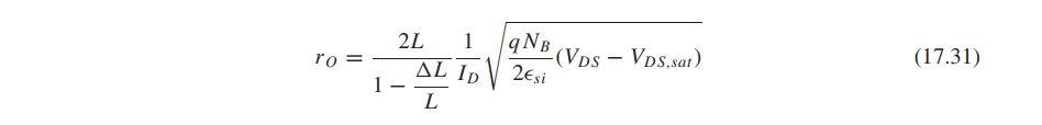
In reality, however, \(r_O\) varies with \(V_{DS}\). As \(V_{DS}\) increases and the pinch-off point moves toward the source, the rate at which the depletion region around the source becomes wider decreases, resulting in a higher incremental output impedance.
Early Voltage indicator
\[ g_m r_o = \frac{g_m}{I_D}I_D \cdot \frac{V_A}{I_D} = \frac{g_m}{I_D} \cdot V_A \]
$g_m r_o $ is the indicator of \(V_A\), if \(\frac{g_m}{I_D}\) is same
Cgd of Common-Source Stage
Miller effect of Cgd during layout
Nonlinearity of Differential Circuits
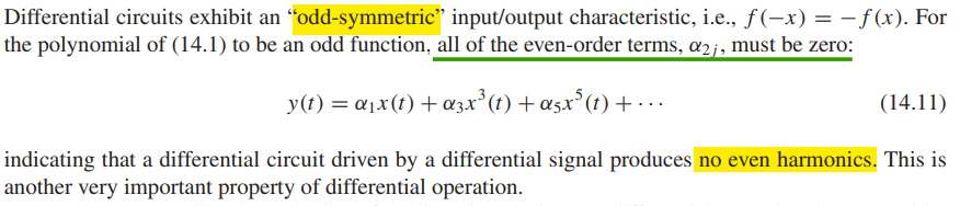
\[ \cos^3\omega t = \frac{3\cos \omega t + \cos(3\omega t)}{4} \]
Zero in differential pair with active current mirror
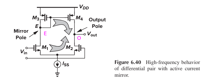
Noting the circuit consists of a "slow path" (M1, M3, M4) in parallel with a "fast path" (M2)
"slow path" \[ H_\text{slow}(s) = \frac{A_0}{(1+s/\omega _{pE})(1+s/\omega _{pO})} \]
"fast path" \[ H_\text{fast}(s) = \frac{A_0}{1+s/\omega _{pO}} \]
Then \[\begin{align} \frac{V_\text{out}}{V_\text{in}} &= H_\text{slow}(s) + H_\text{fast}(s) \\ &= \frac{A_0}{1+s/\omega _{pO}}\left(\frac{1}{1+s/\omega _{pE}} + 1 \right) \\ &= \frac{A_0(1+s/2\omega _{pE})}{(1+s/\omega _{pO})(1+s/\omega _{pE})} \end{align}\]
That is, the system exhibits a zero at \(2\omega_{pE}\)
signals traveling through two paths within an amplifier may cancel each other at one frequency, creating a zero in the transfer function
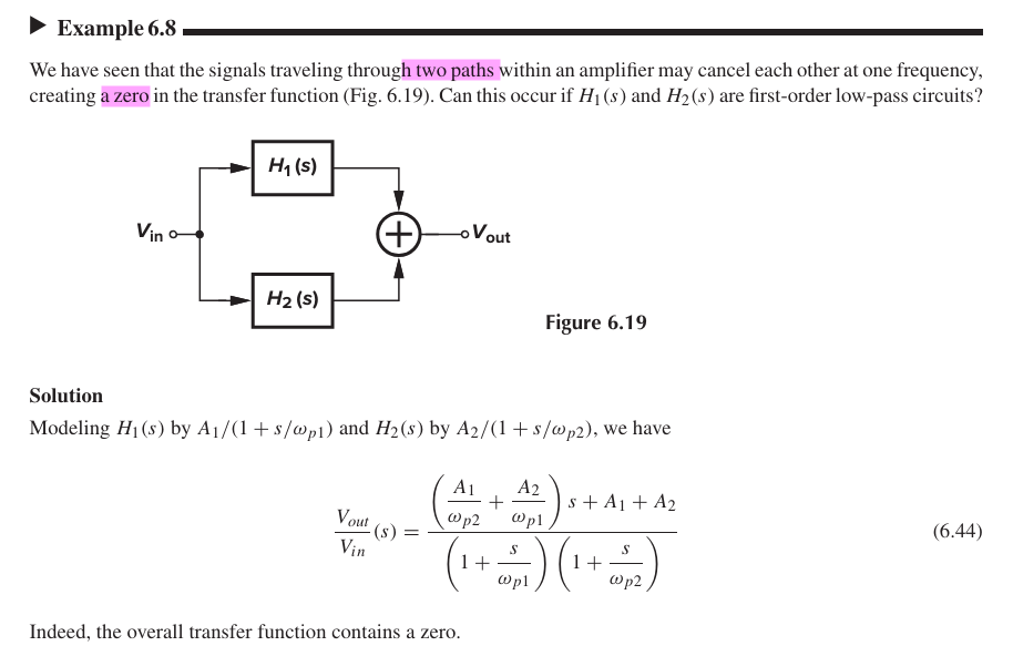
\[ \omega_z = \frac{(A_1+A_2)\omega_{p1}\omega_{p2}}{A_1\omega_{p1}+A_2\omega_{p2}} \] noting \(\omega_{p1}\lt \omega_z \lt \omega_{p2}\)
"Zero" by Inspection
a method to predict the existence of "zero" by inspection, based on the concept of "Analog Phase Interpolation"
TODO 📅
Debashis Dhar, How to Recognize "Zero" by Inspection (Utilizing Analog Phase Interpolation) [https://www.linkedin.com/posts/debashis-dhar-12487024_how-to-recognize-zero-by-inspection-activity-7163364364329160704-9qOq?utm_source=share&utm_medium=member_desktop]
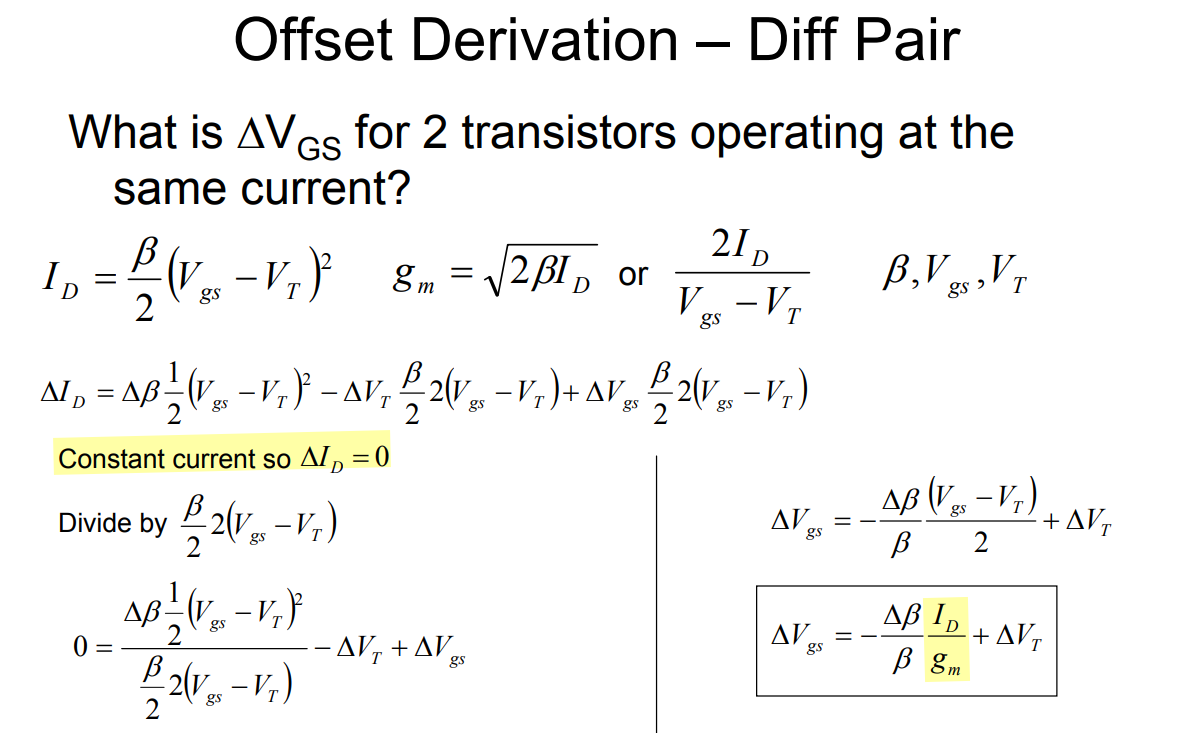
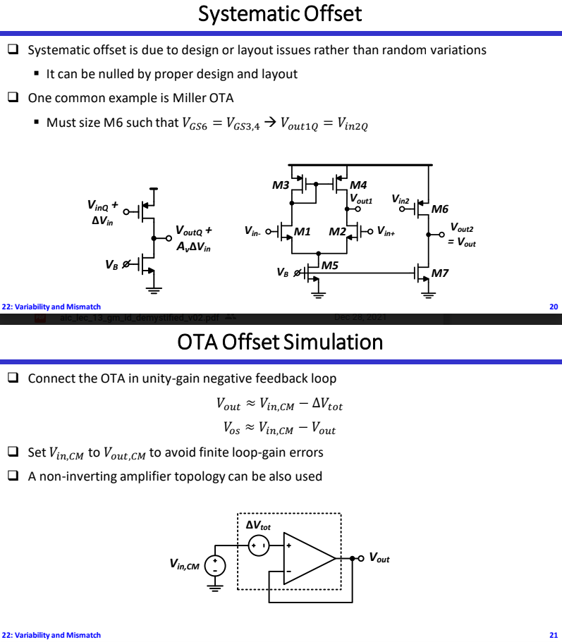
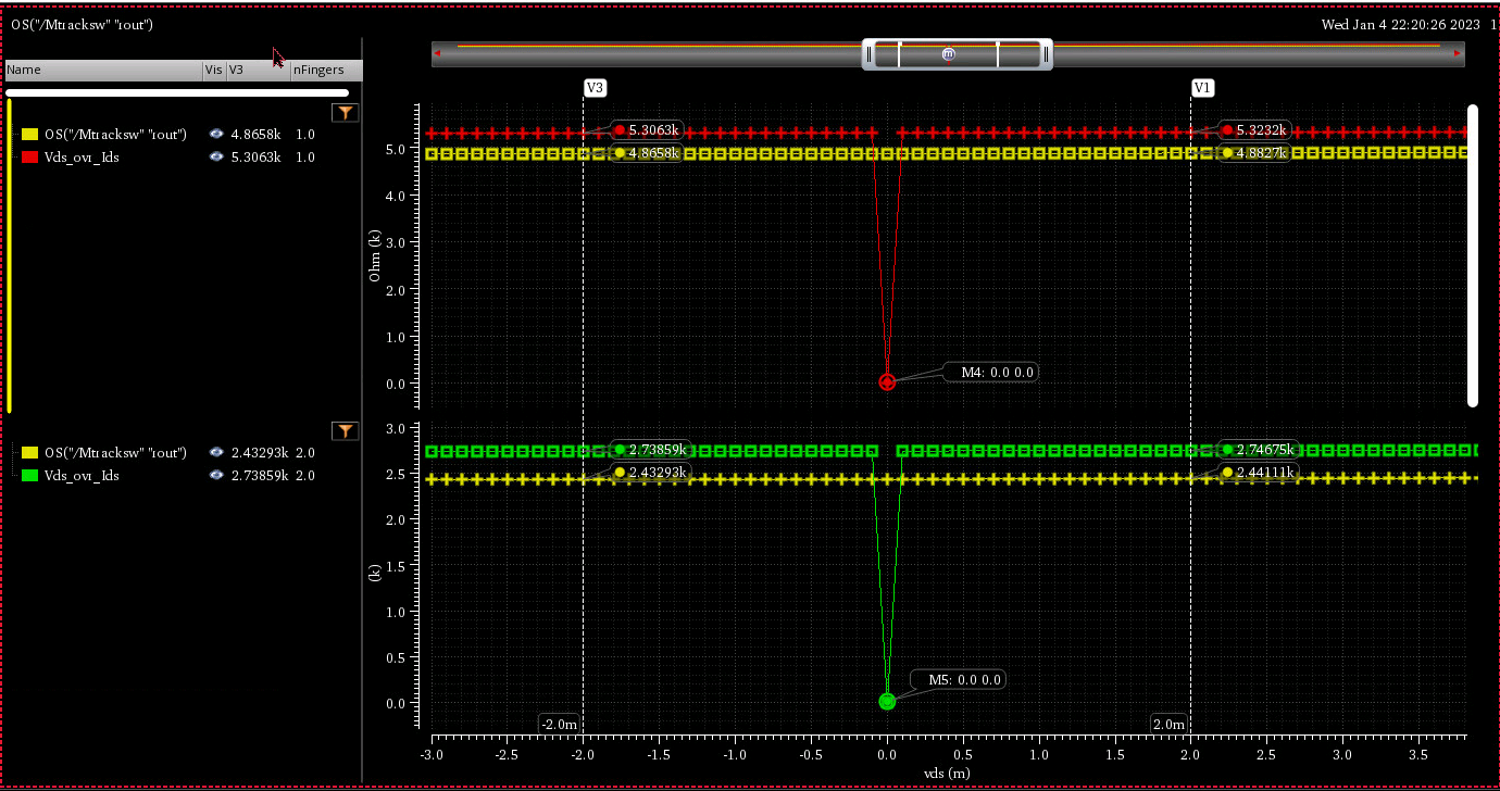
Random offset
Art Zirger, Random Offset in CMOS IC Design [https://designers-guide.org/forum/Attachments/mismatch_presentation.pdf]
The dependence of offset voltage and current mismatches upon the overdrive voltage is similar to our observations for corresponding noise quantities
current mirror
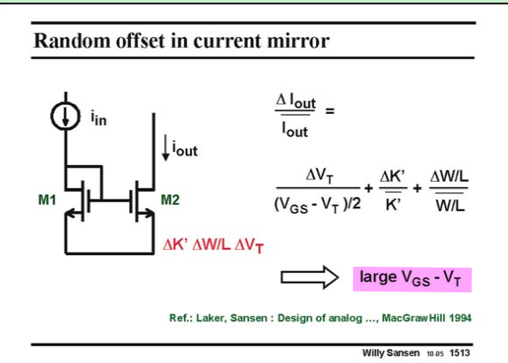
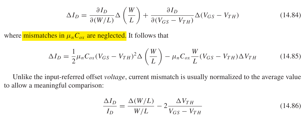
To minimize current mismatch, the overdrive voltage must be maximized, a trend opposite to that in differential pair.
This is because as \(V_{GS}-V_{TH}\) increases, threshold mismatch has a lesser effect on the device currents
\(\Delta I_D= g_m \Delta V_{TH} = \frac{2I_D}{V_{OV}}\Delta V_{TH}\)
differential pair
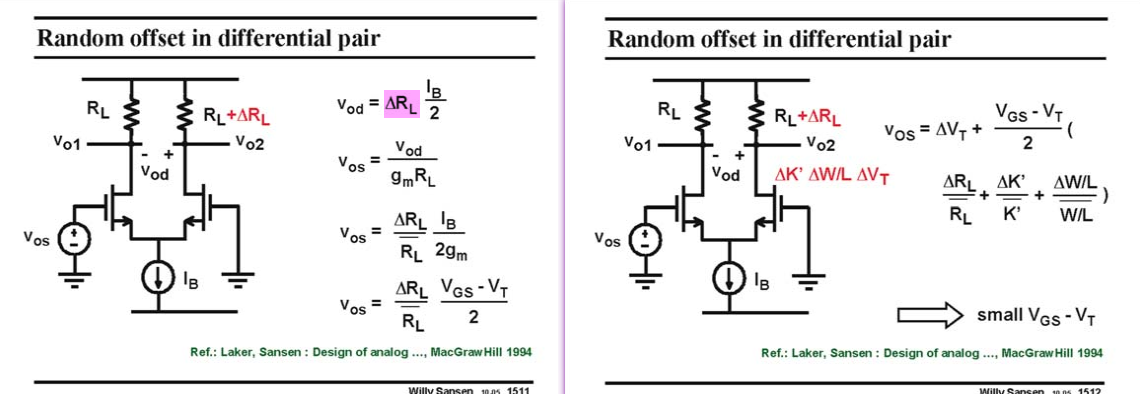
In reality, since mismatches are independent statistical variables
Above shows that the input transistors must be designed for high gain (\(g_mr_o = \frac{2}{V_{OV}\lambda}\)), which means they must be designed for small \(V_{GS}-V_{TH}\).
It is desirable to minimize \(V_{GS}-V_{TH}\) by lowering the tail current or increasing the transistor widths
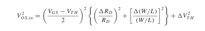
For \(\frac{\Delta K}{K}\)
\[\begin{align} v_{os} g_m &= \Delta K \frac{W}{L}(V_{GS}-V_{TH})^2 \\ v_{os} 2K\frac{W}{L}(V_{GS}-V_{TH}) &= \Delta K \frac{W}{L}(V_{GS}-V_{TH})^2 \\ v_{os} &= \frac{V_{GS}-V_{TH}}{2} \frac{\Delta K}{K} \end{align}\]
The derivation for \(\frac{\Delta W/L}{W/L}\) is same with \(\frac{\Delta K}{K}\)
alternative derivation
\[\begin{align} \Delta V_\beta \cdot g_m &= \frac{\partial I_D}{\partial \beta} \Delta \beta \\ &= I_D \frac{\Delta \beta}{\beta} \end{align}\]
That is \(\Delta V_\beta = \frac{I_D}{g_m}\frac{\Delta \beta}{\beta}\)
\[ \Delta V_R \cdot g_m R = I_D \cdot \Delta R \]
That is \(\Delta V_R = \frac{I_D}{ g_m} \cdot \frac{\Delta R}{R}\)
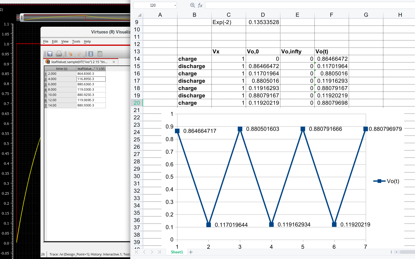
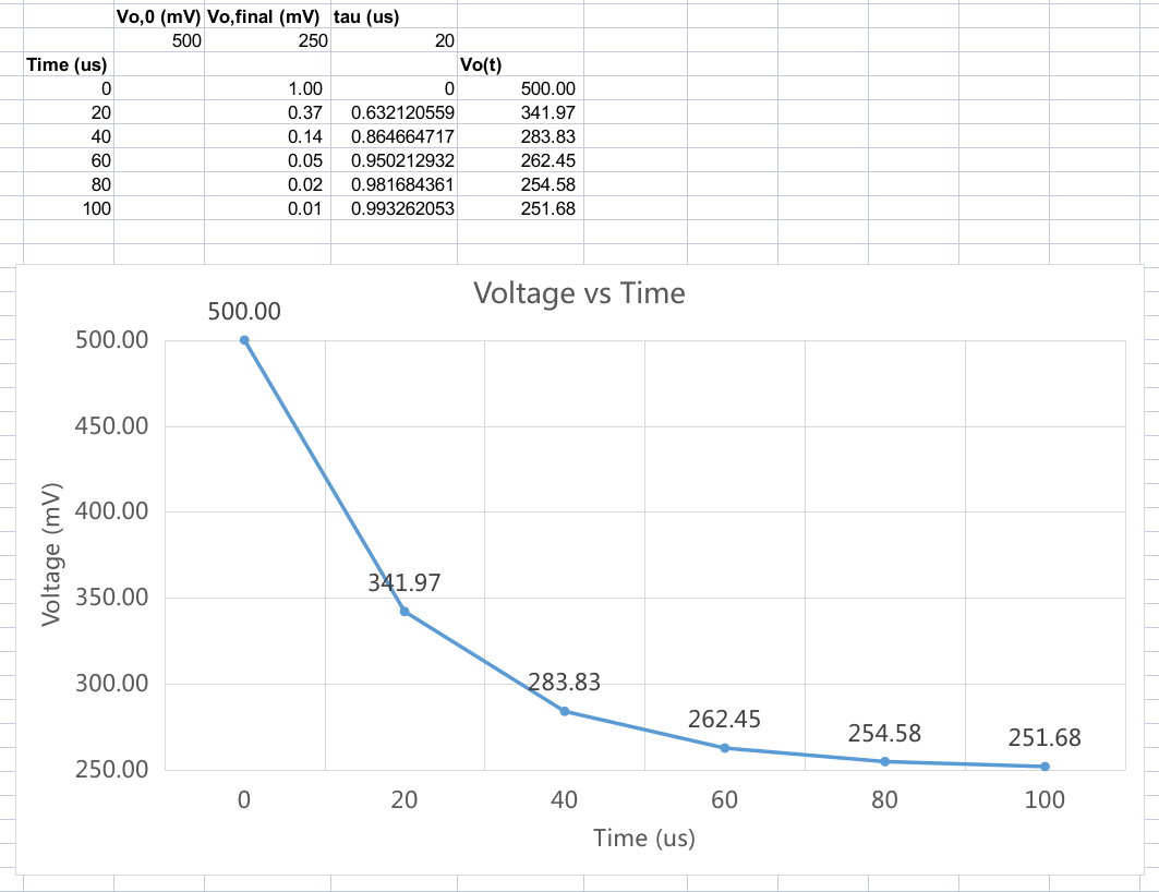
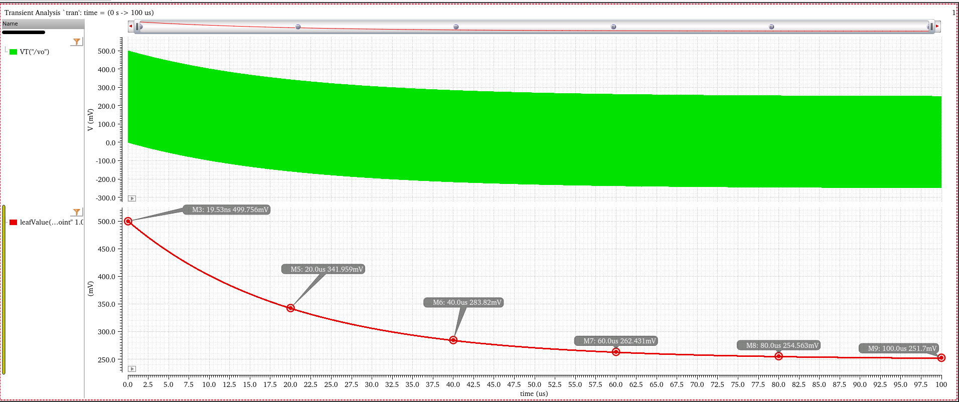
RC charge & discharge
charge: \[ V_o(t) = V_{X}(1-e^{-\frac{t}{\tau}}) + V_{o,0}\cdot e^{\frac{-t}{\tau}} \]
discharge: \[ V_o(t) = V_{o,0}\cdot e^{-\frac{t}{\tau}} + V_{o,\infty}\cdot(1-e^{-\frac{t}{\tau}}) \]
- \(e^{-\frac{t}{\tau}}\) item determine the initial state
- \((1-e^{-\frac{t}{\tau}})\) item determine the final state
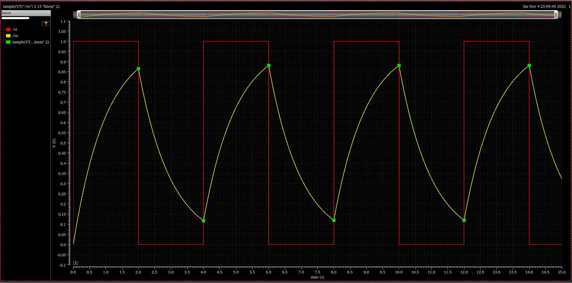
AC coupling
\(V_m=\frac{1}{4},\space \frac{3}{4}\) and its common voltage \(\frac{1}{2}\)
\(V_o=-\frac{1}{4},\space \frac{1}{4}\) and its common voltage \(0\)
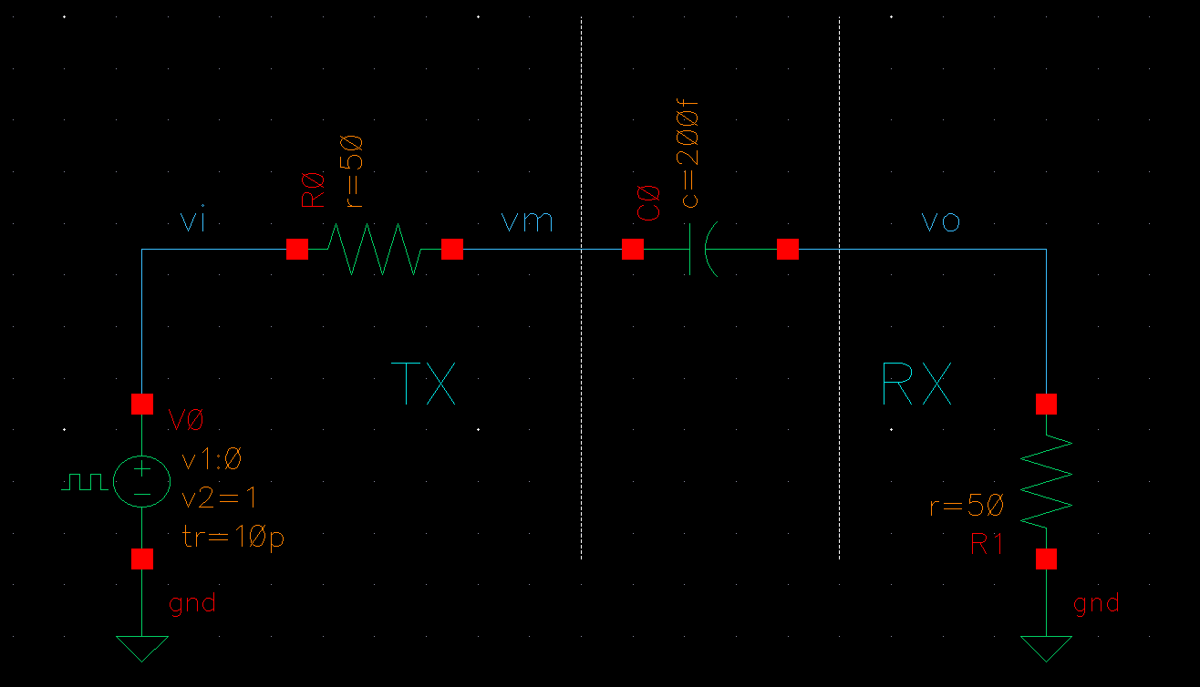
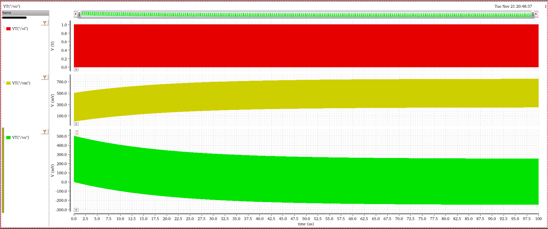
\[ \tau = 200 \text{nF} \times (50+50)\text{ohm} = 20 \mu s \]
high level envelope:
Current mirror with source degeneration
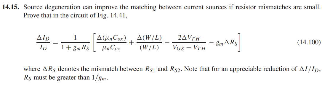
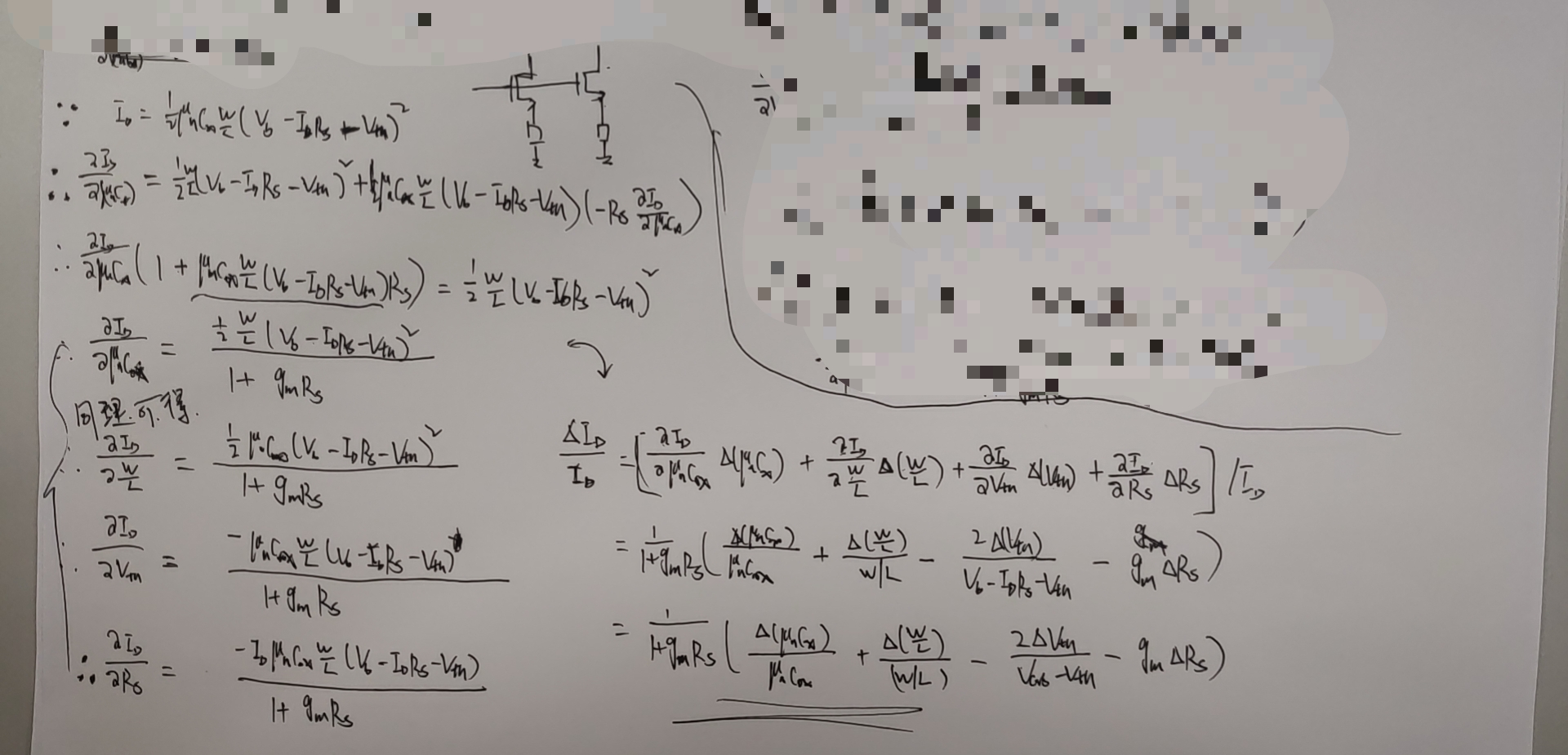
Razavi 2nd, problem 14.15
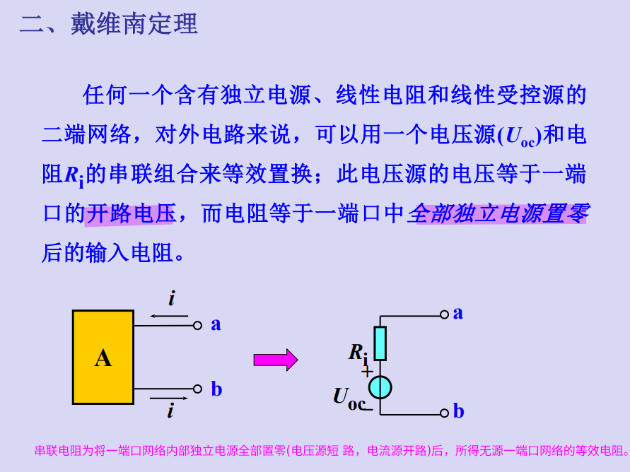
Thevenin and Norton Equivalent Circuits
戴维南定理
等效电阻的计算方法
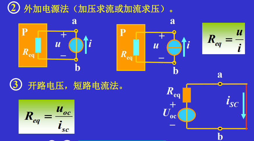
使用外加电源法时, 全部独立电源需要置零
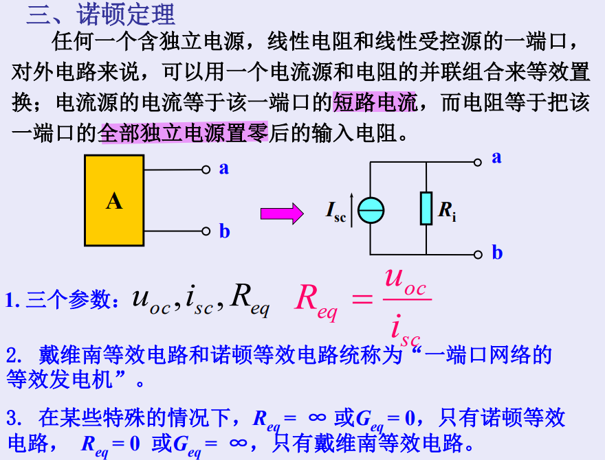
诺顿定理
Miller's Approximation: right-half-plane zero
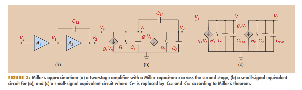
A quick inspection of this circuit reveals that a zero lies at a frequency where the current through \(C_{12}\) becomes equal to \(g_2V_1\).
When this occurs, the current through the parallel combination of \(C_2\) and \(R_2\) becomes zero, creating a zero in the transfer function.
In other words, we can write
\[\begin{align} g_2V_1 &= V_1sC_{12} \\ s &= \frac{g_2}{C_{12}} \end{align}\]
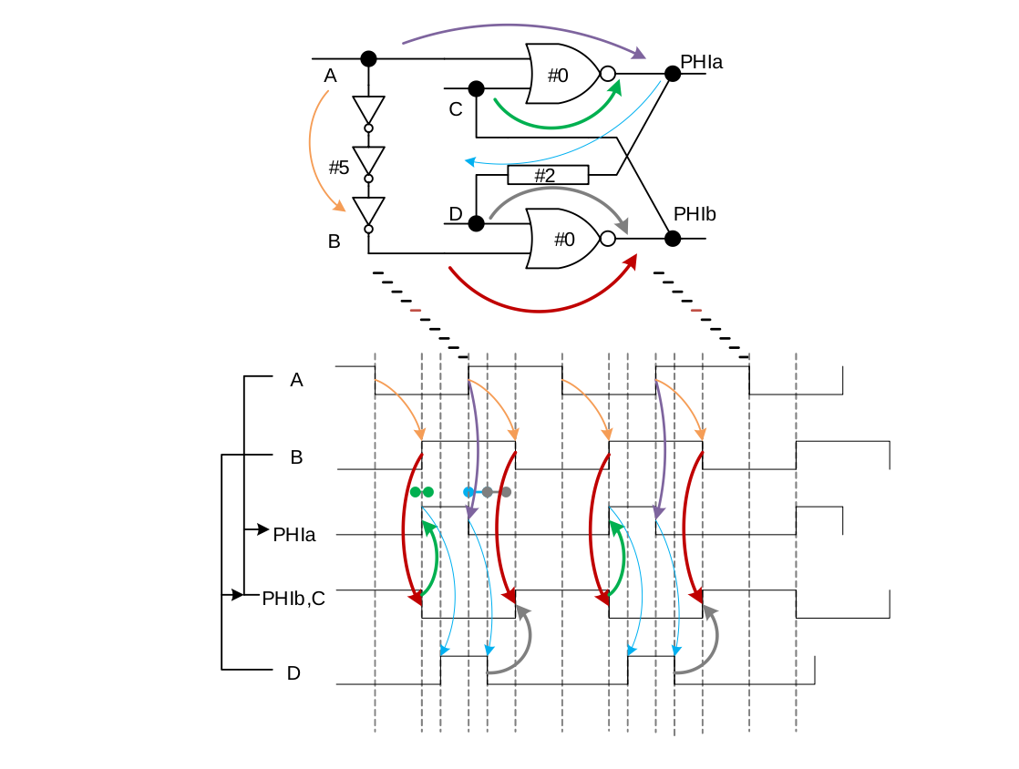
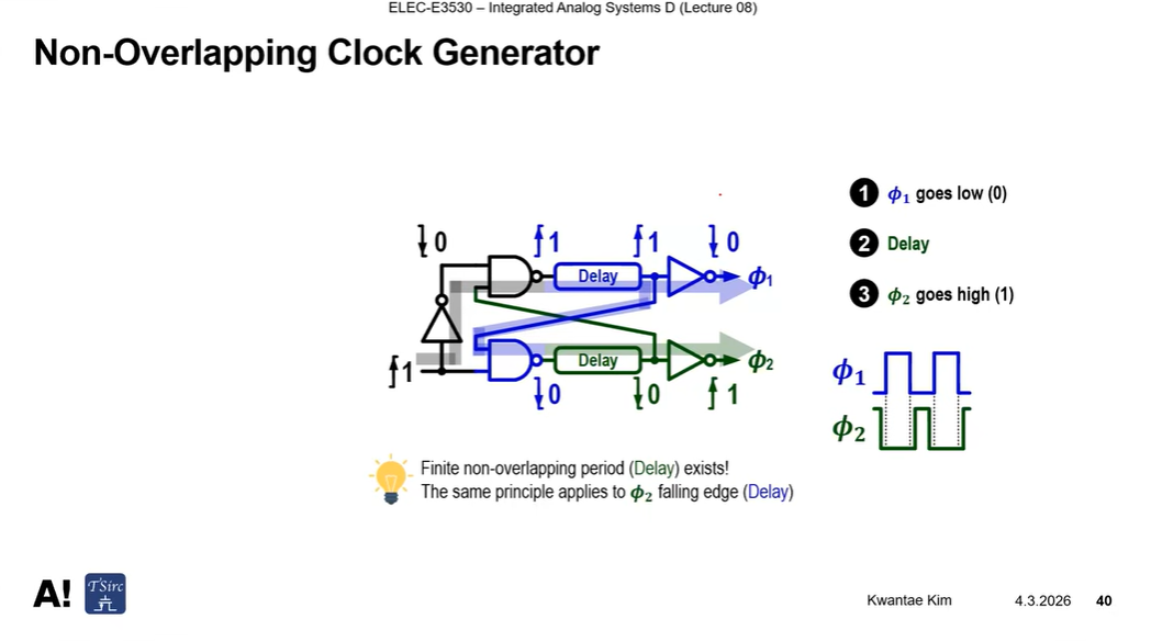
Nonoverlapping clock
Classical
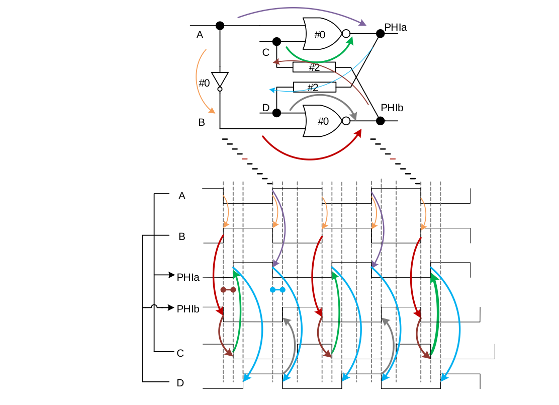
DWC
C2PHIa is important to ensure nonoverlapping and DelayA2B is due to level shifter
Single ended Amplifier Offset Voltage
unity gain buffer
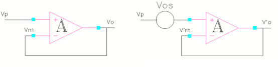
\[\begin{align} V_o &= V_{o,dc}+A(V_p-V_m) \\ V_o' &= V_{o,dc}+A(V_p+V_{os}-V_m') \end{align}\]
Then, we get \[ V_{os}=\frac{V_o'-V_o}{A}+(V_m'-V_m) \] Due to \(V_o=V_m\) and \(V_o'=V_m'\) \[ V_{os}=(1/A+1)\Delta{V_m} \] or \[ V_{os}=(1/A+1)\Delta{V_o} \] if \(A \gg 1\) \[ V_{os}=\Delta{V_o} \]
non-inverting amplifier
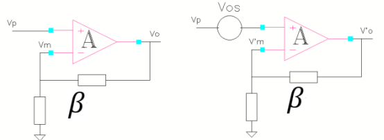 \[\begin{align}
V_o &= V_{o,dc}+A(V_p-V_m) \\
V_o' &= V_{o,dc}+A(V_p+V_{os}-V_m') \\
V_m &= \beta V_o \\
V_m' &= \beta V_o'
\end{align}\]
\[\begin{align}
V_o &= V_{o,dc}+A(V_p-V_m) \\
V_o' &= V_{o,dc}+A(V_p+V_{os}-V_m') \\
V_m &= \beta V_o \\
V_m' &= \beta V_o'
\end{align}\]
we get \[ V_{os}=\frac{V_o'-V_o}{A}+(V_m'-V_m) \] or \[ V_{os}=\frac{\Delta V_o}{A}+\beta \Delta V_o \] if \(A \gg 1\) \[ V_{os}=\beta \Delta V_o \] or \[ V_{os}=\Delta V_m \]
Lecture 22 Variability and Mismatch of Dr. Hesham A. Omran's Analog IC Design
URL: https://www.master-micro.com/professional-courses/analog-ic-design/course-resources
Gotcha MOS ron
There is discrepancy between model operating point and \(V_{ds}/I_{ds}\)
I believe that the equation \(V_{ds}/I_{ds}\) is more appropriate where mos is used as switch, though \(V_{ds}=0\) is an outlier.
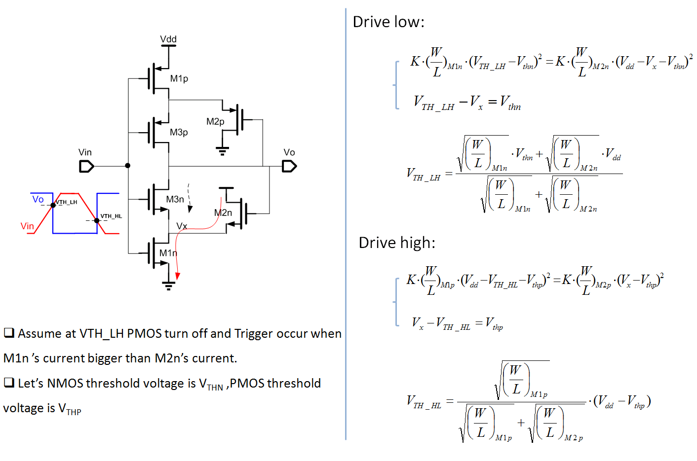
Schmitt Inverter
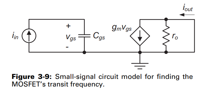
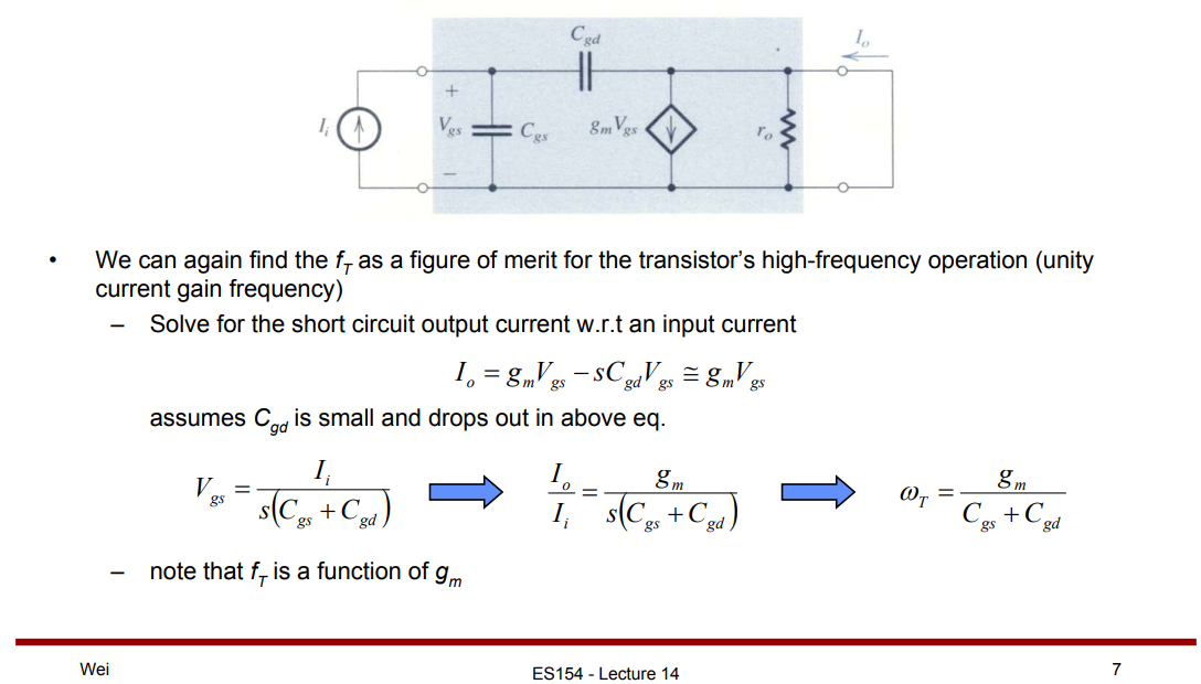
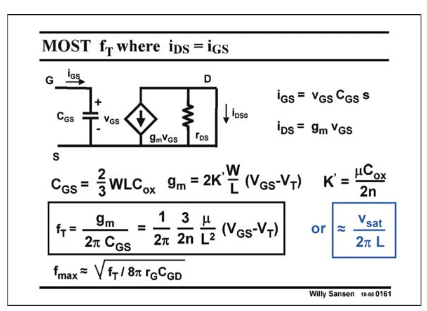
transition frequency \(f_T\)
Defined as the frequency at which the small-signal current gain of a device is unity
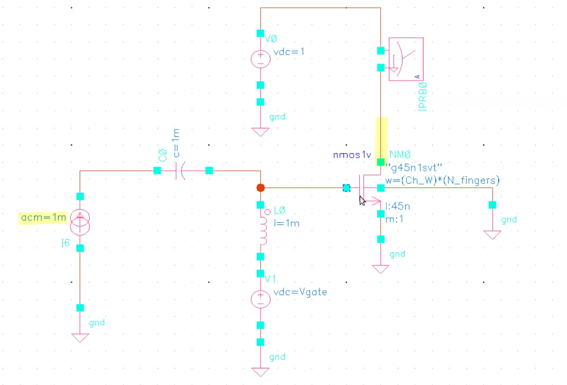
mag(Ids@ft) = Ig(1mA)
Aditya Varma Muppala. MMIC 08: High Frequency Device Characterization in Cadence - Fmax, Ft, NFmin vs Jd [https://youtu.be/kgEypIA8eus]
fmax
Art3, Measuring Fmax for MOS Transistors [https://community.cadence.com/cadence_blogs_8/b/rf/posts/measuring-fmax-for-mos-transistors]
TODO 📅
Miller multiplication of Capacitor
Positive Cap
Negative Cap
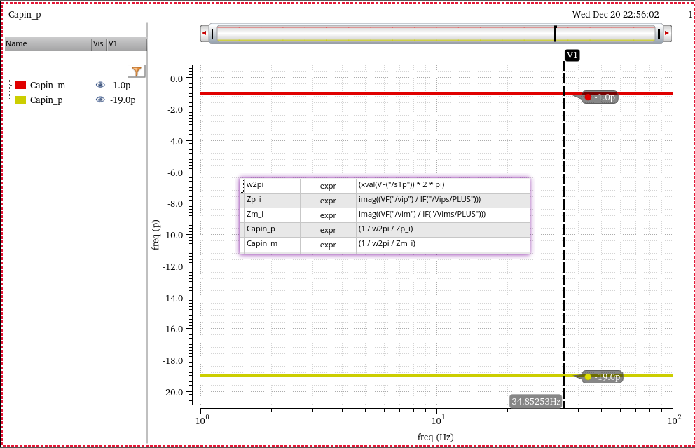
gain has limited bandwidth
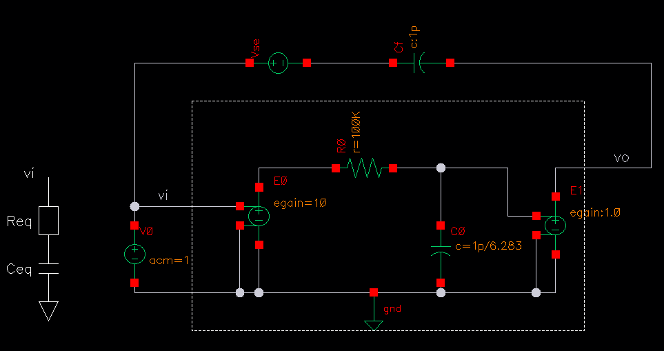
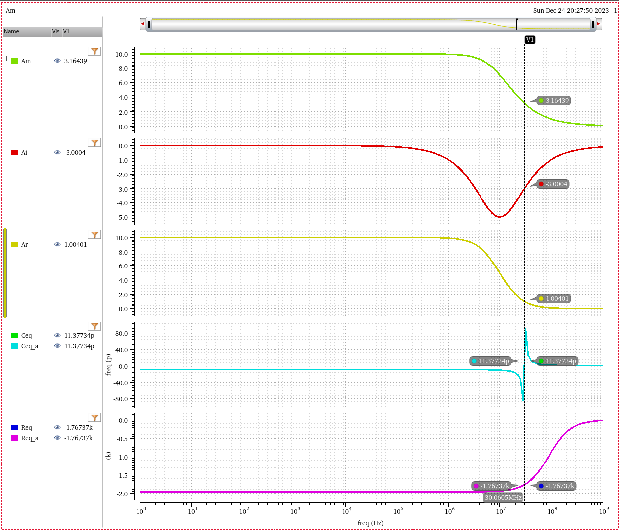
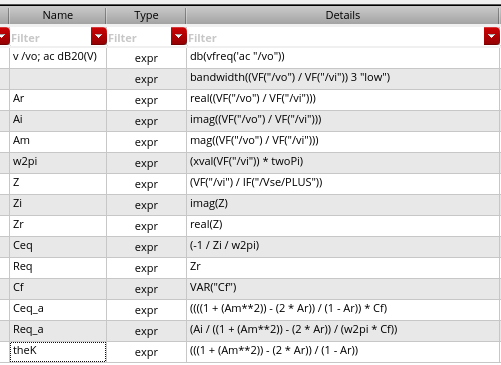
\(V_o = V_i |A|e^{j\theta}\), and \(A_r = |A|\cos\theta\), \(A_i = |A|\sin\theta\)
Then \(I_i = (V_i - V_o)sC_f= V_i(1-|A|e^{j\theta})sC_f\), impedance is shown as below
\[\begin{align} Z &= \frac{V_i}{I_i} \\ &= \frac{1}{(1-|A|e^{j\theta})j\omega C_f} \\ &= -\frac{j}{\omega C_f\frac{1+|A|^2-2|A|\cos\theta}{1-|A|\cos\theta}} + \frac{|A|\sin\theta}{\omega C_f (1+|A|^2-2|A|\cos\theta)} \\ \end{align}\]
\(C_\text{eq}\) and \(R_\text{eq}\) are obtained \[\begin{align} C_\text{eq} &= \frac{1+|A|^2-2A_r}{1-A_r}\cdot C_f \\ R_\text{eq} &= \frac{A_i}{1+|A|^2-2A_r}\cdot \frac{1}{\omega C_f} \end{align}\]
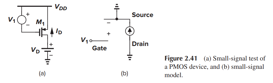
D/S small signal model
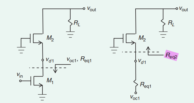
The
DrainandSourceof MOS are determined in DC operating point, i.e. large signal.
That is, top of \(M_2\) is
drain and bottom is source, \[\begin{align}
R_\text{eq2} &= \frac{r_\text{o2}+R_L}{1+g_\text{m2}r_\text{o2}} \\
& \simeq \frac{1}{g_\text{m2}}
\end{align}\]
PMOS small signal model polarity
The small-signal models of NMOS and PMOS transistors are identical
A negative \(\Delta V_\text{GS}\) leads to a negative \(\Delta I_D\).
Recall that \(I_D\), in the direction shown here, is negative because the actual current of holes flows from the source to the drain.
Conversely, a positive \(\Delta V_\text{GS}\) produces a positive \(\Delta I_D\), as is the case for an NMOS device.
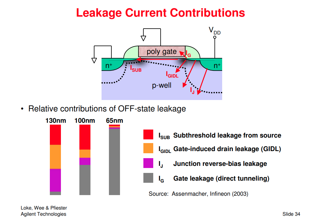
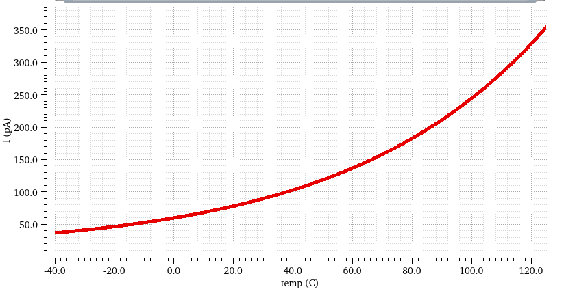
Leakage in MOS
Alvin L.S. Loke. 2004. Introduction to Deep Submicron CMOS Device Technology & Its Impact on Circuit Design [https://ewh.ieee.org/r5/denver/sscs/Presentations/2004_12_Loke.pdf]
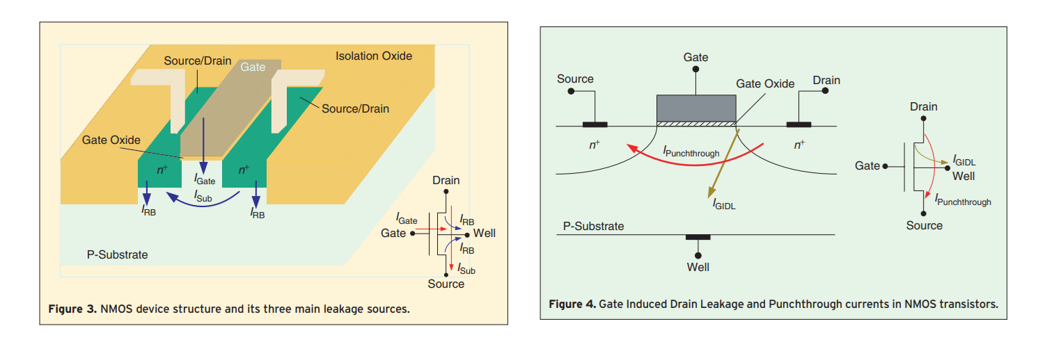
- Subthreshold leakage
- Drain-Induced Barrier Lowering (DIBL)
- Reverse-bias Source/Drain junction leakages
- Gate leakage
- two other leakage mechanisms
- Gate Induced Drain Leakage (GIDL)
- Punchthrough
W. M. Elgharbawy and M. A. Bayoumi, "Leakage sources and possible solutions in nanometer CMOS technologies," in IEEE Circuits and Systems Magazine, vol. 5, no. 4, pp. 6-17, Fourth Quarter 2005, doi: 10.1109/MCAS.2005.1550165.
X. Qi et al., "Efficient subthreshold leakage current optimization - Leakage current optimization and layout migration for 90- and 65- nm ASIC libraries," in IEEE Circuits and Devices Magazine, vol. 22, no. 5, pp. 39-47, Sept.-Oct. 2006, doi: 10.1109/MCD.2006.272999.
P. Monsurró, S. Pennisi, G. Scotti and A. Trifiletti, "Exploiting the Body of MOS Devices for High Performance Analog Design," in IEEE Circuits and Systems Magazine, vol. 11, no. 4, pp. 8-23, Fourthquarter 2011, doi: 10.1109/MCAS.2011.942751.
Andrea Baschirotto, ISSCC2015 "ADC Design in Scaled Technologies"
Joachim Assenmacher Infineon Technologies, "BSIM4 Modeling and Parameter Extraction" [https://ewh.ieee.org/r5/denver/sscs/References/2003_03_Assenmacher.pdf]
Stefan Rusu, Intel ISSCC 2008 Tutorial: "Leakage Reduction Techniques" [https://www.nishanchettri.com/isscc-slides/2008%20ISSCC/Tutorials/T06_Pres.pdf]
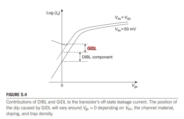
Drain-Induced Barrier Lowering (DIBL)

As a result of DIBL, threshold voltage is reduced with shorter channel lengths and, consequently, the subthreshold leakage current is increased
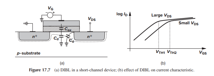
impact on output impedance
The principal impact of DIBL on circuit design is the degraded output impedance.
In short-channel devices, as \(V_{DS}\) increases further, drain-induced barrier lowering becomes significant, reducing the threshold voltage and increasing the drain current
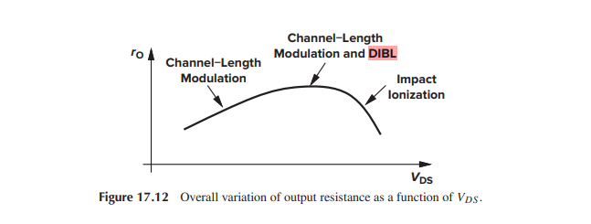
Impact Ionization and GIDL are different, however both increase drain current, which flowing from the drain into the substrate
Gate induced drain leakage (GIDL)
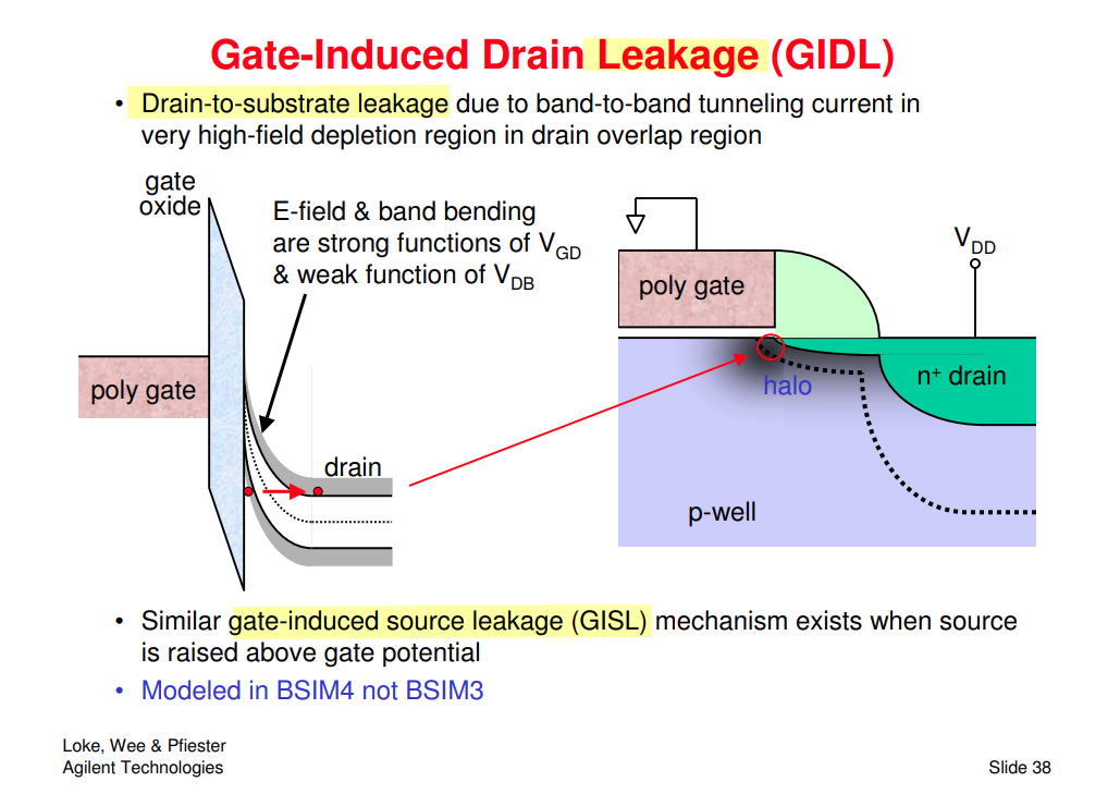
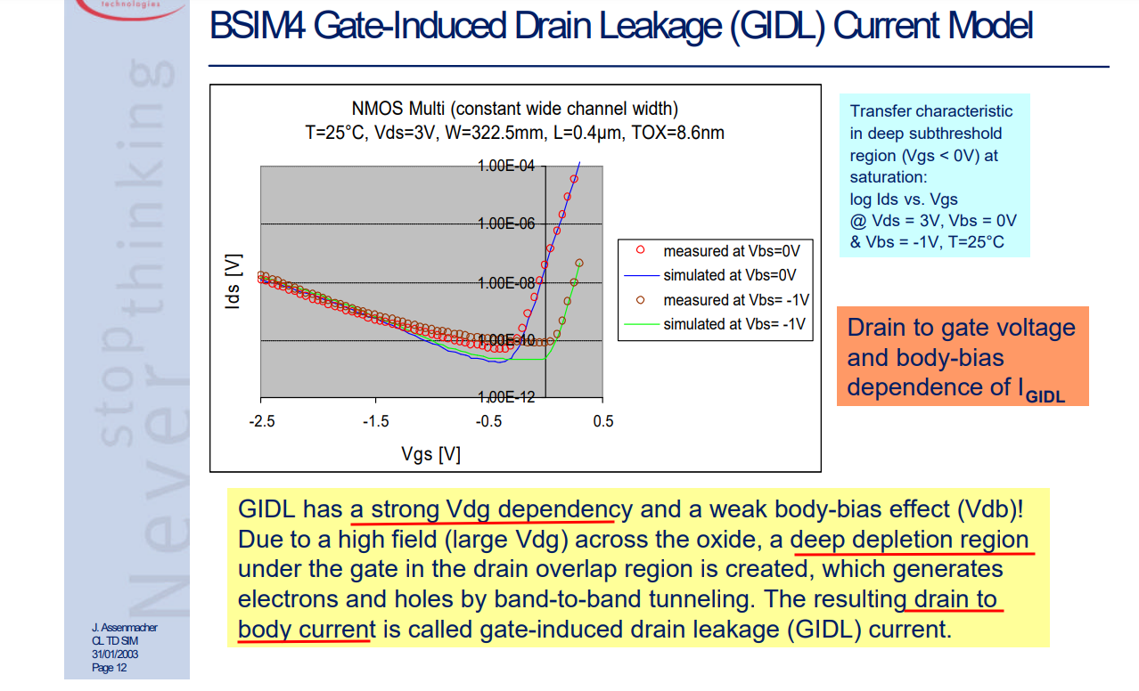
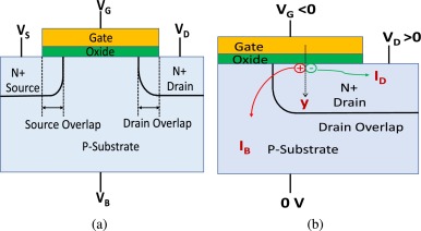
The large current flows from the drain to bulk and this drain leakage current is named gate-induced drain leakage (GIDL) since it is due to a gate-induced high electric field present in the gate-to-drain overlap region
gate-induced drain leakage (GIDL) increases exponentially due to the reduced gate oxide thickness
Chauhan, Yogesh Singh, et al. FinFET modeling for IC simulation and design: using the BSIM-CMG standard. Academic Press, 2015.
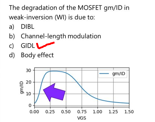
\[ \frac{g_m}{I_D} = \frac{2}{V_{GS}-V_{TH}} \] Decrease of gm/Id results from decrease in VT.
GIDL (Gate induced drain leakage) as at weak inversion may results in a weak lateral electric field causing leakage current between drain and bulk, which degrade the efficiency of the transistor (gm/ID).
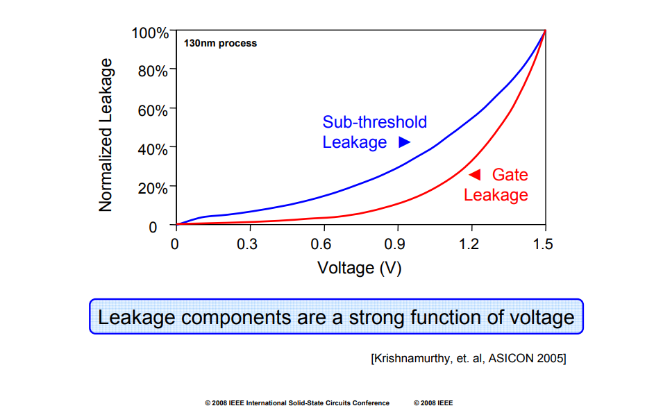
Voltage Dependence
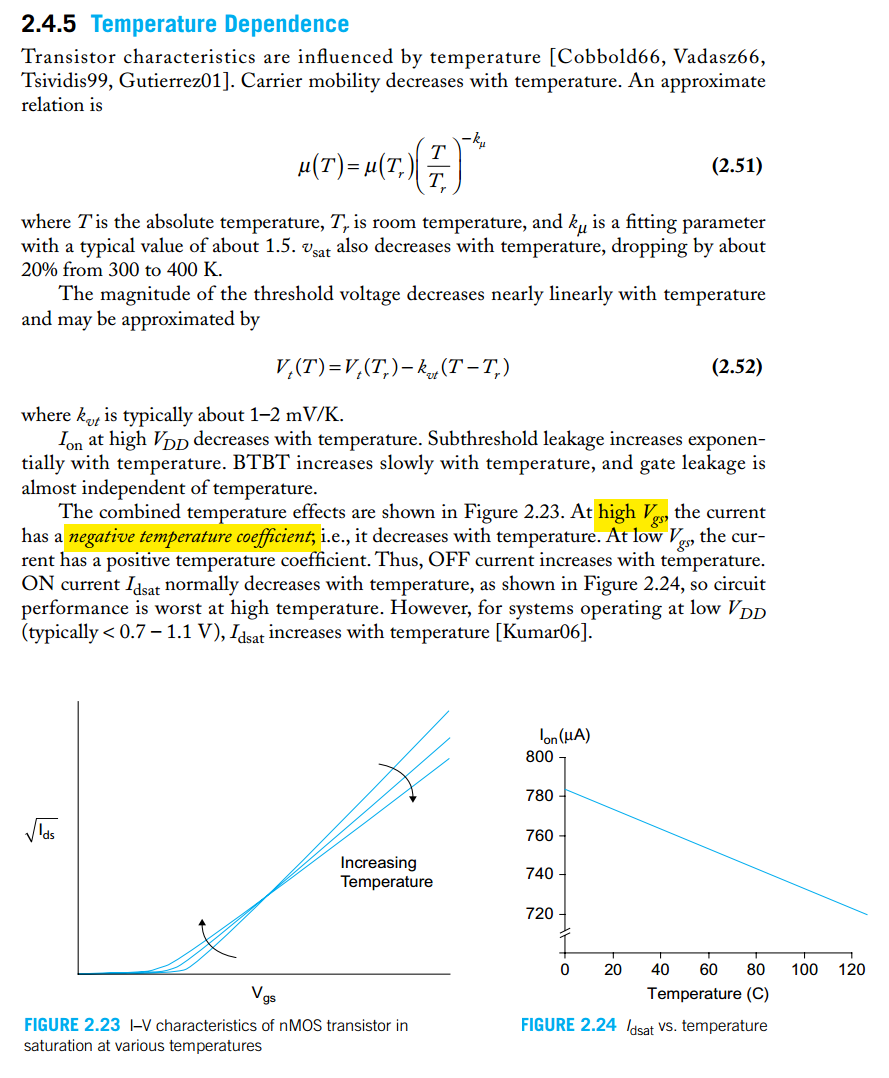
Temperature Dependence
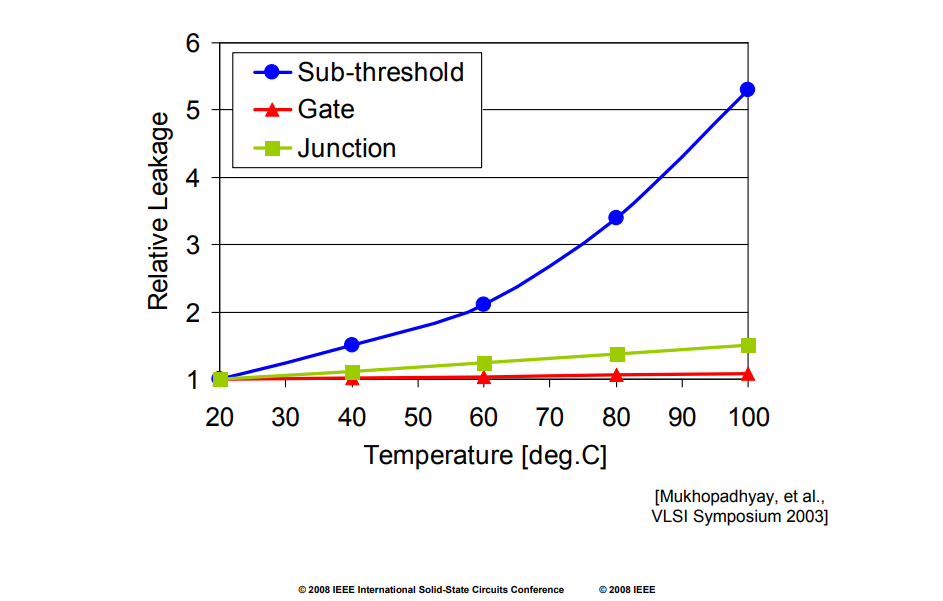
In advanced node, gate leakage is also a strong function of temperature
Power/Ground and I/O Pins
Power / Ground Pin Information
In both digital and analog I/O, power and ground pins appear at the sub-circuit definiton, allowing user to use the I/O in voltage islands. They follow certain naming conventions.
- digital I/O sub-circuit
- VDD: pre-driver core voltage (supplied by PVDD1CDGM)
- VSS: pre-driver ground and also global ground (supplied by PVDD1CDGM)
- VDDPST: I/O post-driver voltage, i.e. 1.8V (supplied by PVDD2CDGM or PVDD2POCM)
- VSSPOST: I/O post-driver ground (supplied by PVDD2CDGM or PVDD2POCM)
- POCCTRL: POCCTRL signal (supplied by PVDD2POCM)
- analog I/O placed in a core voltage domain, the convention is
- TACVDD: analog core voltage (supplied by PVDD3ACM)
- TACVSS: analog core ground (supplied by PVDD3ACM)
- VSS: global core ground
- analog I/O placed in an I/O voltage domain, the convention is:
- TAVDD: analog I/O voltage, i.e. 1.8V (supplied by PVDD3AM)
- TAVSS: analog I/O ground (supplied by PVDD3AM)
- VSS: global core ground
Power/Ground Combo Cells
| power/ground combo pad cell | pins to be connected to bump | to core side pin name |
|---|---|---|
| PVDD1CDGM | VDD VSS | VDD VSS |
| PVDD2CDGM PVDD2POCM | VDDPST VSSPST | N/A |
| PVDD3AM | TAVDD TAVSS | AVDD AVSS |
| PVDD3ACM | TACVDD TACVSS | AVDD AVSS |
Note for the retention mode
- At initial state, IRTE must be 0 when VDD is off.
- IRTE must be kept >= 10us after VDD turns on again (from the retention mode to the normal operation mode).
- IRTE can be switched only when both VDD and VDDPST are on.

When the rention function is needed, IRTE signal must come from an "always-on" core power domain. If you don't need the rention function, it is required to tie IRTE to ground. In other words, no matter the rention feature is needed or not, it is required to have PCBRTE in each domain.

Note: PCBRTE does not need PAD connection.
Internal Pins
There are 3 internal global pins, i.e. ESD, POCCTRL, RTE, in all digital domain cells.
In real application,
- ESD pin is an internal signal and active in ESD event happening
- POCCTRL is an internal signal and active in Power-on-control event.
However, these special events (i.e. ESD event and Power-on-control event) are not modeled in NLDM kit (.lib), only normal function is covered, so ESD and POCCTRL pins are simply defined as ground in NLDM kit (.lib).
These 3 global pins will be connected automatically after cell-to-cell abutting in physical layout.
Power-Up sequence in Digital Domain
Power up the I/O power (VDDPST) first, then the core power (VDD)

- PVDDD2POCM cell would generate Power-On-Control signal (POCCTRL) to have the post-driver NMOS and PMOS off, so that the crowbar current would not occur in the post-driver fingers when the I/O voltage is on while the core voltage remains off. As such, I/O cell would be in the Hi-Z state. when POCCTRL is on, the pll-up/down resistor is disabled and C is 0.
- The POCCTRL signal is transmitted to I/O cells through cell abutment. There is no need to have routing for POCCTTRL nor give a control signal to the POCCTRL pin any of I/O cells. Note that the POCCTRL signal would be cut if inserting a power-cut (PRCUT) cell.

Power-Down sequence in Digital Domain
It's the reverse of power-up sequence.
Use model in Innovus
1 | set init_gnd_net "vss_core vss DUMMY_ESD DUMMY_POCCTRL" |
1 | set pins [get_object_name [get_ports *]] |
reference
The Analog Designer's Toolbox (ADT) | Invited Talk by IEEE Santa Clara Valley Section CAS Society, https://youtu.be/FT6kKC5OdE0
ESSCIRC2023 Circuit Insights Ali Sheikholeslami [https://youtu.be/2xFIZM5_FPw]
Ali Sheikholeslami, Circuit Intuitions: Thevenin and Norton Equivalent Circuits, Part 3 IEEE Solid-State Circuits Magazine, Vol. 10, Issue 4, pp. 7-8, Fall 2018.
—, Circuit Intuitions: Thevenin and Norton Equivalent Circuits, Part 2 IEEE Solid-State Circuits Magazine, Vol. 10, Issue 3, pp. 7-8, Summer 2018.
—, Circuit Intuitions: Thevenin and Norton Equivalent Circuits, Part 1 IEEE Solid-State Circuits Magazine, Vol. 10, Issue 2, pp. 7-8, Spring 2018.
—, Circuit Intuitions: Miller's Approximation IEEE Solid-State Circuits Magazine, Vol. 7, Issue 4, pp. 7-8, Fall 2015.
—, Circuit Intuitions: Miller's Theorem IEEE Solid-State Circuits Magazine, Vol. 7, Issue 3, pp. 8-10, Summer 2015.
Shanthi Pavan, "Demystifying Linear Time Varying Circuits"
ecircuitcenter. Switched-Capacitor Resistor [http://www.ecircuitcenter.com/Circuits/SWCap/SWCap.htm]
Jørgen Andreas Michaelsen. INF4420 Switched-Capacitor Circuits. [https://www.uio.no/studier/emner/matnat/ifi/INF4420/v13/undervisningsmateriale/inf4420_v13_07_switchedcapacitor_print.pdf]
chembiyan T. OC Lecture 10: A very basic introduction to switched capacitor circuits [https://youtu.be/SaYtemYp4rQ
Robert Bogdan Staszewski, Poras T. Balsara. "All‐Digital Frequency Synthesizer in Deep‐Submicron CMOS"
Mayank Parasrampuria, Sandeep Jain, Burn-in 101 [link]
Kevin Zheng. Circuit Artists [https://circuit-artists.com/posts/]