Deep N-well
Substrate noise
A variety of techniques can be used to minimize this noise, for example by keeping analog devices surrounded by guard rings, or using a separate supply for the substrate/well taps.
However guard rings alone cannot prevent noise coupling deep in the substrate, only surface currents.
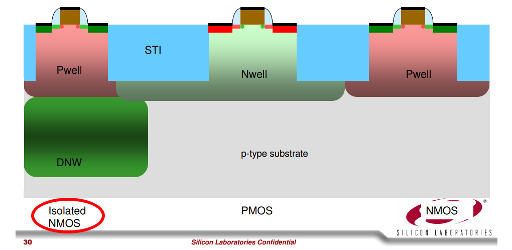
PMOS are less noisy than NMOS since PMOS has its nwell which isolates the substrate noise, but such is not valid for NMOS .
DNW
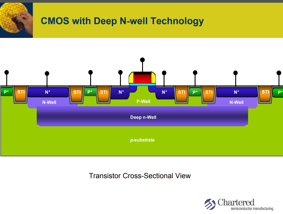
The N-channel devices built directly into the P-type substrate are not as effectively isolated as P-channel devices in their N-wells. This is because despite creating a P+ guard ring around the devices, there remains an electrical path below the guard ring for charge to flow.
To overcome this issue, a deep N-well can be used to more effectively isolate these N-channel devices.
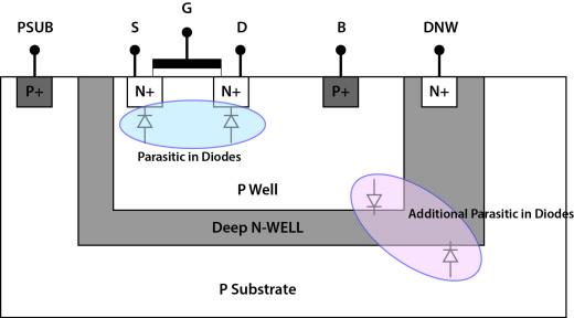
pwdnw: PW/DNW diode
dnwpsub: DNW/PSUB diode
Together At Last – Combining Netlist and Layout Data for Power-Aware Verification
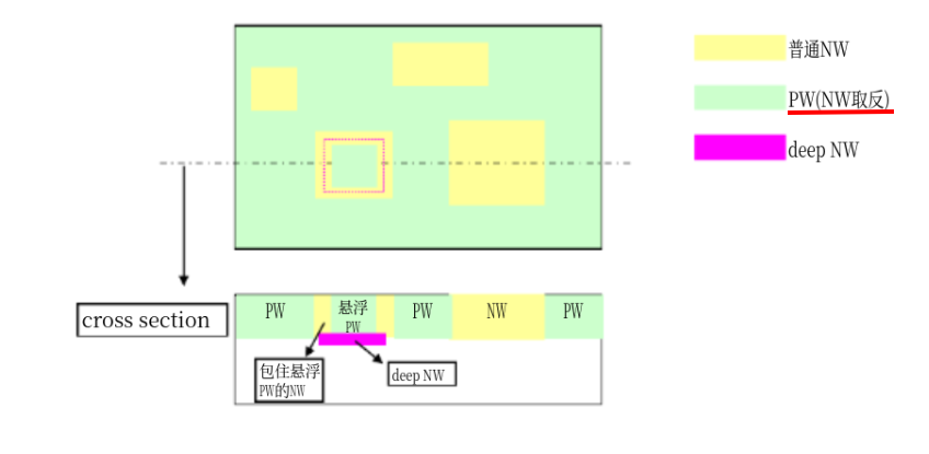
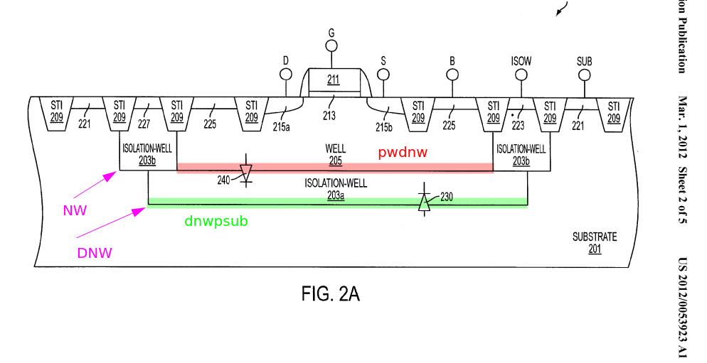
- the P-well is separated, allowing the voltage to be controlled
- because the circuit within the deep N-well is separated from the p-substrate in this structure, there is the benefit that this circuitry is less susceptible to noise that propagates through the p-substrate.
reference
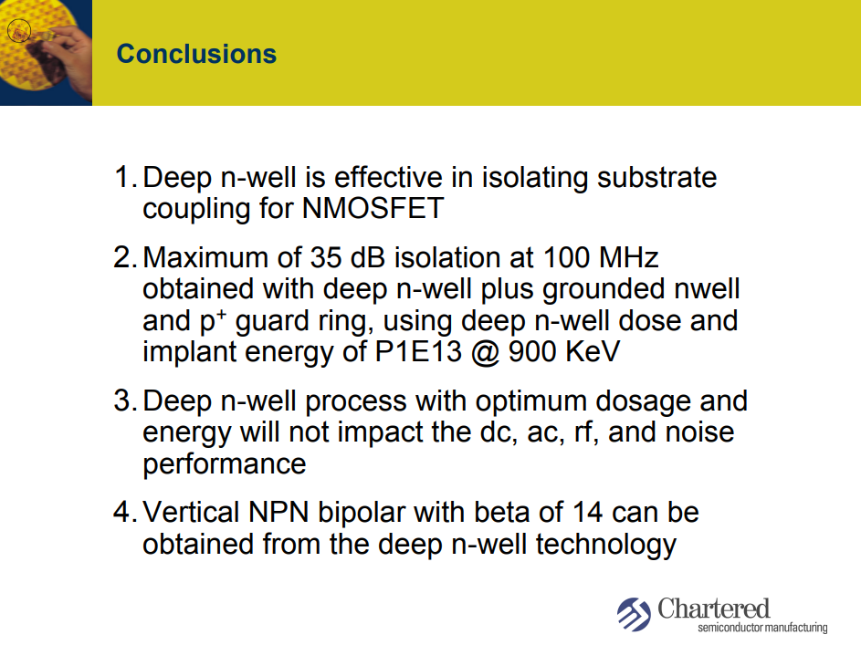
Chew, K.W., Zhang, J., Shao, K., Loh, W., & Chu, S.F. (2002). Impact of Deep N-well Implantation on Substrate Noise Coupling and RF Transistor Performance for Systems-on-a-Chip Integration. 32nd European Solid-State Device Research Conference, 251-254. URL:[slides, paper]
Mark Waller, Analog layout: Why wells, taps, and guard rings are crucial
KEITH SABINE Using Deep N Wells in Analog Design
Faricelli, J. (2010). Layout-dependent proximity effects in deep nanoscale CMOS. IEEE Custom Integrated Circuits Conference 2010, 1-8.
cmos_processing, URL:http://users.ece.utexas.edu/~athomsen/cmos_processing.pdf
Kuo-Tsai LiPaul ChangAndy Chang, TSMC, US20120053923A1, "Methods of designing integrated circuits and systems thereof"