Native NMOS Blocked Implant (NT_N)
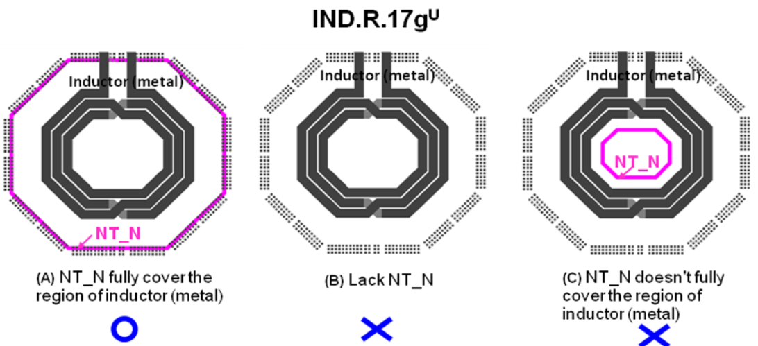
A native layer (NT_N) is usually added under inductors or transformers in the nanoscale CMOS to define the non-doped high-resistance region of substrate, which decreases eddy currents in the substrate thus maintaining high Q of the coils.
For T* PDK offered inductor, a native substrate region is created under the inductor coil to minimize eddy currents
OD inside NT_N only can be used for NT_N potential pickup purpose, such as the guarding-ring of MOM and inductor
Derived Geometries
| Term | Definition |
|---|---|
| PW | {NOT NW} |
| N+OD | {NP AND OD} |
| P+OD | {PP AND OD} |
| GATE | {PO AND OD} |
| TrGATE | {GATE NOT PODE_GATE} |
NP: N+ Source/Drain Ion Implantation
PP: P+ Source/Drain Ion Implantation
OD: Gate Oxide and Diffustion
NW: N-WELL
PW: P-WELL
CMOS Processing Technology
Four main CMOS technologies:
- n-well process
- p-well process
- twin-tub process
- silicon on insulator
Triple well, Deep N-Well (optional):
- NWell: NMOS svt, lvt, ulvt ...
- PWell: PMOS svt, lvt, ulvt ...
- DNW: For isolating P-Well from the substrate
The NT_N drawn layer adds no process cost and no extra mask
The N-well / P-well technology, where n-type diffusion is done over a p-type substrate or p-type diffusion is done over n-type substrate respectively.
The Twin well technology, where NMOS and PMOS transistor are developed over the wafer by simultaneous diffusion over an epitaxial growth base, rather than a substrate.
reference
Principles of VLSI Design CMOS Processing CMPE 413 [https://redirect.cs.umbc.edu/~cpatel2/links/315/lectures/chap3_lect09_processing2.pdf]
CMOS processing [http://users.ece.utexas.edu/~athomsen/cmos_processing.pdf]
The Fabrication Process of CMOS Transistor [https://www.elprocus.com/the-fabrication-process-of-cmos-transistor/#:~:text=latch%2Dup%20susceptibility.-,N%2D%20well%2F%20P%2D%20well%20Technology,well%20it%20is%20vice%2D%20verse.]