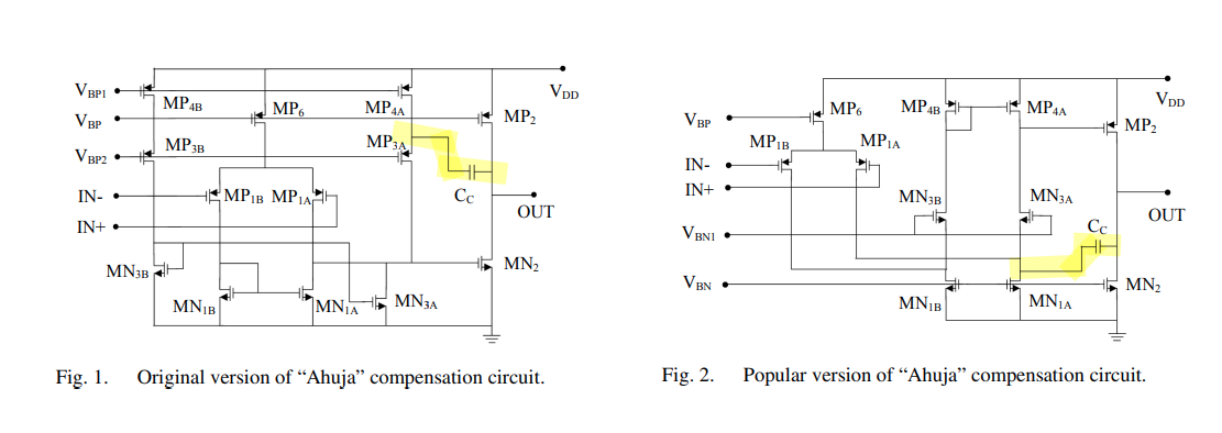
ahuja compensation
This cascode compensation topology is popularly known as ahuja compensation
The cause of the positive zero is the feedforward current through \(C_m\).
To abolish this zero, we have to cut the feedforward path and create a unidirectional feedback through \(C_m\).
Adding a resistor(nulling resistor) is one way to mitigate the effect of the feedforward current.
Another approach uses a current buffer cascode to pass the small-signal feedback current but cut the feedforward current
People name this approach after the author Ahuja
The benefits of Ahuja compensation over Miller compensation are severa
better PSRR
higher unity-gain bandwidth using smaller compensation capacitor
ability to cope better with heavy capacitive and resistive loads
Miller's approximation
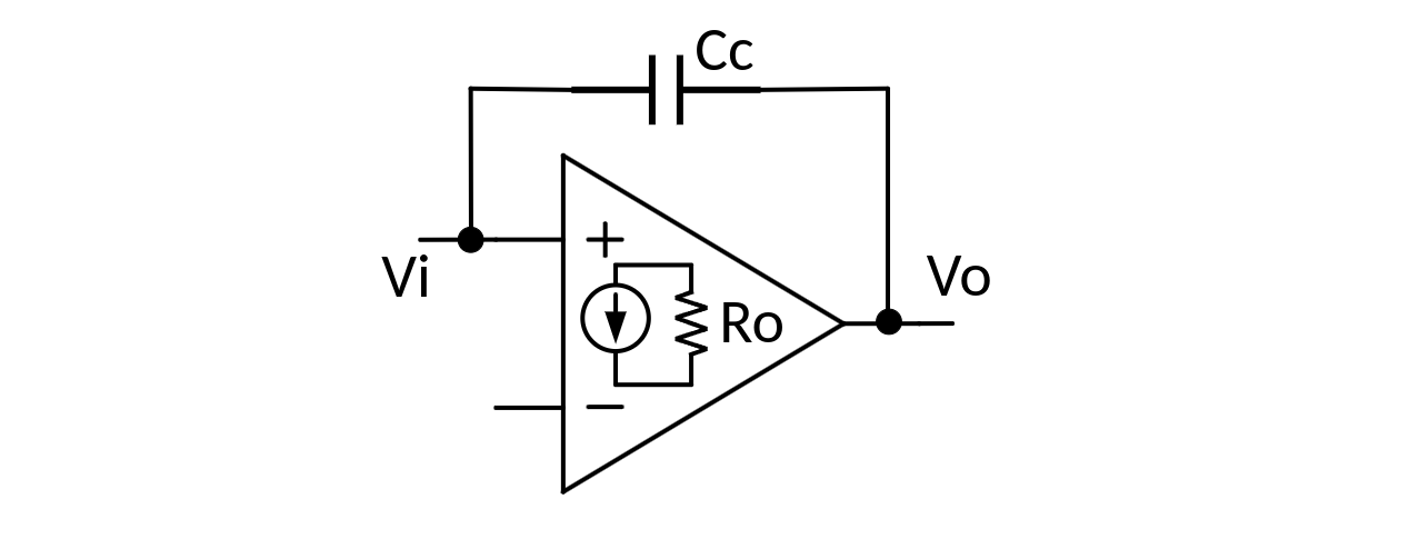
Right-Half-Plane Zero
\[ \left[(v_i - v_o)sC_c - g_m v_i\right]R_o = v_o \] Then \[ \frac{v_o}{v_i} = -g_mR_o\frac{1-s\frac{C_c}{g_m}}{1+sR_oC_c} \] right-half-plane Zero \(\omega _z = \frac{g_m}{C_c}\)
Equivalent cap
The amplifier gain magnitude \(A_v = g_m R_o\) \[ I_\text{c,in} = (v_i - v_o)sC_c \] Then \[\begin{align} I_\text{c,in} &= (v_i + A_v v_i)sC_c \\ & = v_i s (1+A_v)C_c \end{align}\]
we get \(C_\text{in,eq}= (1+A_v)C_c\simeq A_vC_c\)
Similarly \[\begin{align} I_\text{c,out} &= (v_o - v_i)sC_c \\ & = v_o s (1+\frac{1}{A_v})C_c \end{align}\]
we get \(C_\text{out,eq}= (1+\frac{1}{A_v})C_c\simeq C_c\)
cascode compensation
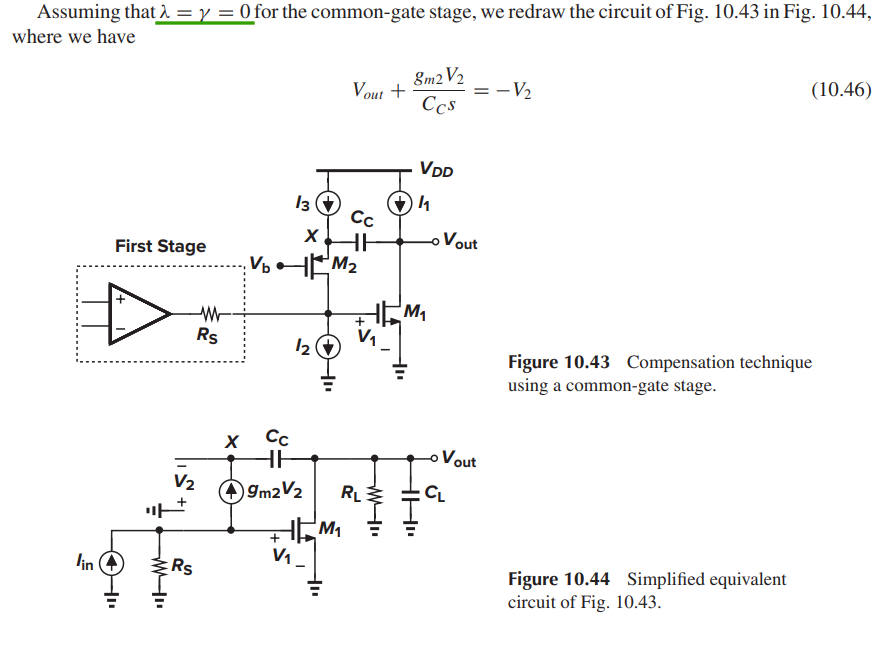
Of course, , if the capacitance at the gate of \(M_1\) is taken into account, pole splitting is less pronounced.
including \(r_\text{o2}\)
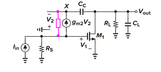 \[
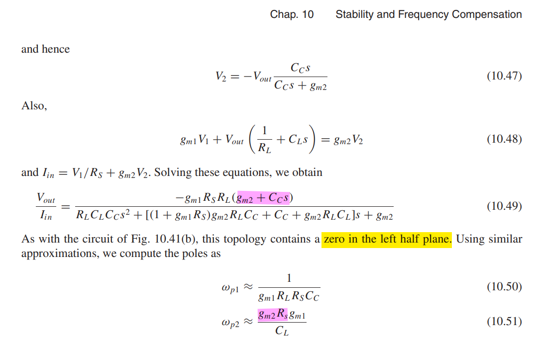
\frac{V_{out}}{I_{in}} \approx
\frac{-g_{m1}R_SR_L(g_{m2}+C_Cs)}{\frac{R_S+r_\text{o2}}{r_\text{o2}}R_LC_LC_Cs^2+g_{m1}g_{m2}R_LR_SC_Cs+g_{m2}}
\] The poles as
\[
\frac{V_{out}}{I_{in}} \approx
\frac{-g_{m1}R_SR_L(g_{m2}+C_Cs)}{\frac{R_S+r_\text{o2}}{r_\text{o2}}R_LC_LC_Cs^2+g_{m1}g_{m2}R_LR_SC_Cs+g_{m2}}
\] The poles as
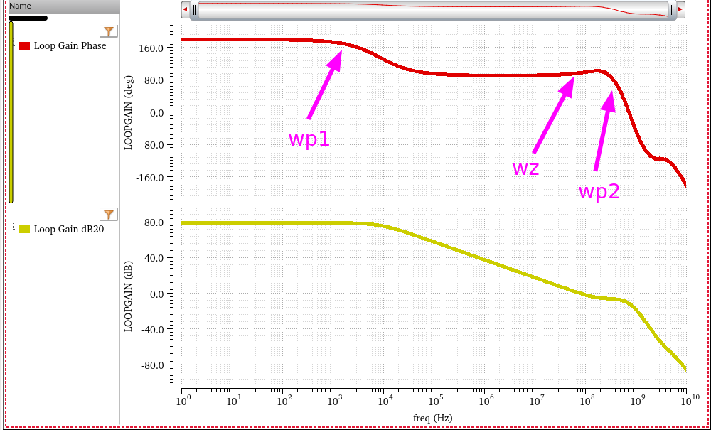
\[\begin{align} \omega_{p1} &\approx \frac{1}{g_{m1}R_LR_SC_c} \\ \omega_{p2} &\approx \frac{g_{m2}R_Sg_{m1}}{C_L}\frac{r_\text{o2}}{R_S+r_\text{o2}} \end{align}\]
and zero is not affected, which is \(\omega_z =\frac{g_{m2}}{C_C}\)
the above model simulation result is shown below
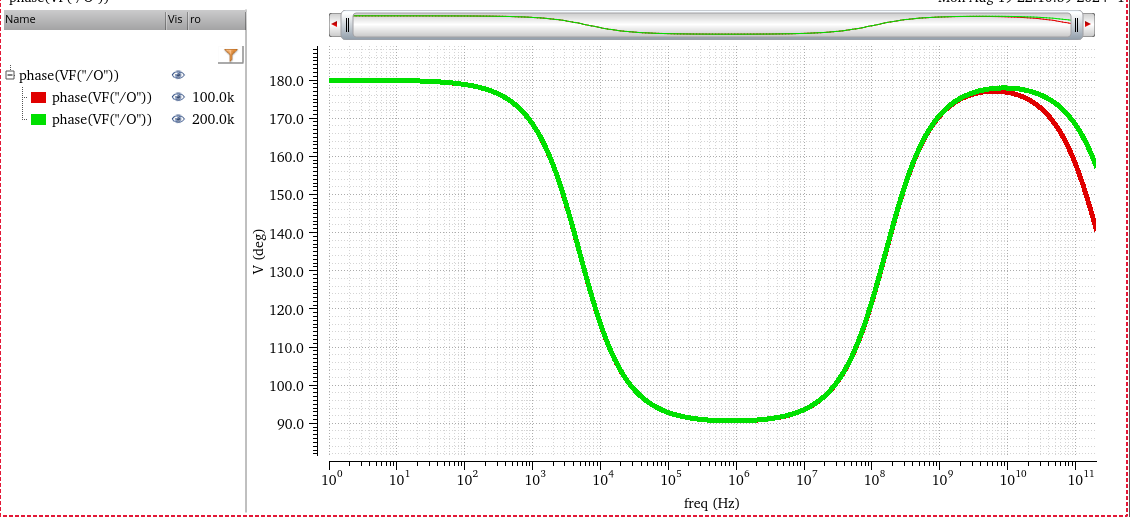
the zero is located between two poles
take into the capacitance at the gate of \(M_1\) and all other second-order effect
intuitive analysis of zero
miller compensation
- zero in the right half plane \[ g_\text{m1}V_P = sC_c V_P \]
cascode compensation
- zero in the left half plane \[ g_\text{m2}V_X = - sC_c V_X \]

How to Mitigate Impact of Zero
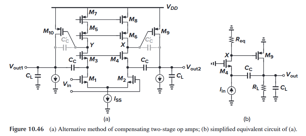
dominant pole \[ \omega_\text{p,d} = \frac {1} {R_\text{eq}g_\text{m9}R_{L}C_{c}} \] first nondominant pole \[ \omega_\text{p,nd} = \frac {g_\text{m4}R_\text{eq}g_\text{m9}} {C_L} \] zero \[ \omega_\text{z} = (g_\text{m4}R_\text{eq})(\frac {g_\text{m9}} {C_c}) \] a much greater magnitude than \(g_\text{m9}/C_C\)
Lectures
EE 240B: Advanced Analog Circuit Design, Prof. Bernhard E. Boser [OTA II, Multi-Stage]
Papers
B. K. Ahuja, "An improved frequency compensation technique for CMOS operational amplifiers," in IEEE Journal of Solid-State Circuits, vol. 18, no. 6, pp. 629-633, Dec. 1983, doi: 10.1109/JSSC.1983.1052012.
D. B. Ribner and M. A. Copeland, "Design techniques for cascoded CMOS op amps with improved PSRR and common-mode input range," in IEEE Journal of Solid-State Circuits, vol. 19, no. 6, pp. 919-925, Dec. 1984, doi: 10.1109/JSSC.1984.1052246.
Abo, Andrew & Gray, Paul. (1999). A 1.5V, 10-bit, 14MS/s CMOS Pipeline Analog-to-Digital Converter.
Book's chapters
Design of analog CMOS integrated circuits, Behzad Razavi
- 10.5 Compensation of Two-Stage Op Amps
- 10.7 Other Compensation Techniques
Analog Design Essentials, Willy M.C. Sansen
- chapter #5 Stability of operational amplifiers - Compensation of positive zero
Analysis and Design of Analog Integrated Circuits 5th Edition, Paul R. Gray, Paul J. Hurst, Stephen H. Lewis, Robert G. Meyer
- 9.4.3 Two-Stage MOS Amplifier Compensation
CMOS Analog Circuit Design 3rd Edition, Phillip E. Allen, Douglas R. Holberg
- 6.2.2 Miller Compensation of the Two-Stage Op Amp
Ahuja variations
reference
B. K. Ahuja, "An Improved Frequency Compensation Technique for CMOS Operational Amplifiers," IEEE 1. Solid-State Circuits, vol. 18, no. 6, pp. 629-633, Dec. 1983. [https://sci-hub.se/10.1109/JSSC.1983.1052012]
U. Dasgupta, "Issues in "Ahuja" frequency compensation technique", IEEE International Symposium on Radio-Frequency Integration Technology, 2009. [https://sci-hub.se/10.1109/RFIT.2009.5383679]
R. 1. Reay and G. T. A. Kovacs, "An unconditionally stable two-stage CMOS amplifier," IEEE 1. Solid-State Circuits, vol. 30, no. 5, pp. 591- 594, May 1995.
A. Garimella and P. M. Furth, "Frequency compensation techniques for op-amps and LDOs: A tutorial overview," 2011 IEEE 54th International Midwest Symposium on Circuits and Systems (MWSCAS), 2011, pp. 1-4, doi: 10.1109/MWSCAS.2011.6026315.
H. Aminzadeh, R. Lotfi and S. Rahimian, "Design Guidelines for Two-Stage Cascode-Compensated Operational Amplifiers," 2006 13th IEEE International Conference on Electronics, Circuits and Systems, 2006, pp. 264-267, doi: 10.1109/ICECS.2006.379776.
H. Aminzadeh and K. Mafinezhad, "On the power efficiency of cascode compensation over Miller compensation in two-stage operational amplifiers," Proceeding of the 13th international symposium on Low power electronics and design (ISLPED '08), Bangalore, India, 2008, pp. 283-288, doi: 10.1145/1393921.1393995.
Stabilizing a 2-Stage Amplifier URL:https://a2d2ic.wordpress.com/2016/11/10/stabilizing-a-2-stage-amplifier/