Asynchronous SAR ADC
assign the amount of time based on the time needed for each step
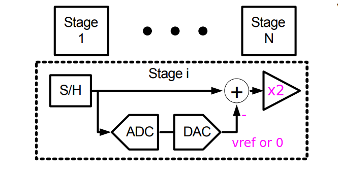
pipeline ADC

\[ V_{N-1} = \sum_{i=0}^{N-2} B[i]\frac{1}{2^{N-i}}+ B[N-1]\frac{1}{2} \] Compare with \(\frac{1}{2}\), and determine \(B[N-1]\) \[\begin{align} V_{N-2} &= \left(V_{N-1} - B[N-1]\frac{1}{2}\right)\cdot 2 \\ &= \left(\sum_{i=0}^{N-1} B[i]\frac{1}{2^{N-i}} - B[N-1]\frac{1}{2}\right) \cdot 2 \\ &= \sum_{i=0}^{N-2} B[i]\frac{1}{2^{N-i}} \cdot 2 \\ &= \sum_{i=0}^{N-3} B[i]\frac{1}{2^{N-i}}\cdot 2 + B[N-2]\frac{1}{2} \end{align}\]
On your intuition, input can be expressed as below \[\begin{align} V_{N-1} &= \sum_{i=0}^{N-1} B[i] \frac{1}{2}\cdot 2^{i-N+1} \\ &= B[N-1]\frac{1}{2} + B[N-2]\frac{1}{2}\cdot 2^{-1} + B[N-3]\frac{1}{2}\cdot 2^{-2 }... \end{align}\]
It divides the process into several comparison stages, the number of which is proportional to the number of bits
Due to the pipeline structure of both analog and digital signal path, inter-stage residue amplification is needed which consumes considerable power and limits high speed operation
reduced residue amplification gain
Synchronous SAR ADC
It also divides a full conversion into several comparison stages in a way similar to the pipeline ADC, except the algorithm is executed sequentially rather than in parallel as in the pipeline case.
However, the sequential operation of the SA algorithm has traditionally been a limitation in achieving high-speed operation
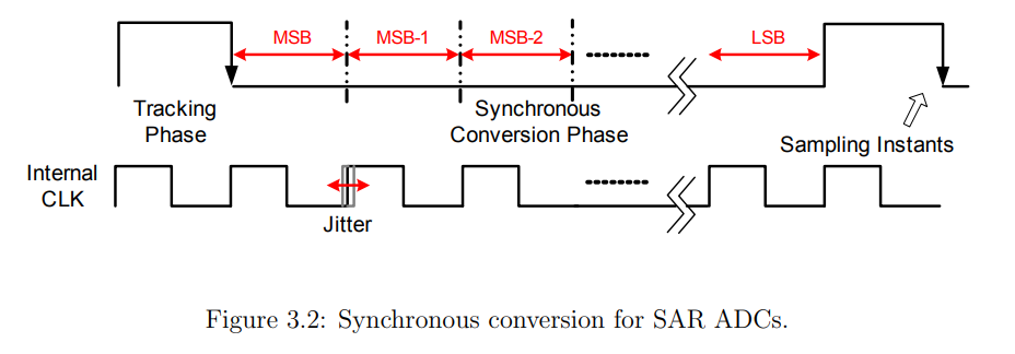
- a clock running at least \((N + 1) \cdot F_s\) is required for an \(N\)-bit converter with conversion rate of \(F_s\)
- every clock cycle has to tolerate the worst case comparison time
- every clock cycle requires margin for the clock jitter
The power and speed limitations of a synchronous SA design comes largely from the high-speed internal clock
Non-Binary Successive Approximation
The overlapped search range compensates for wrong decisions made in earlier stages as long as they are within the error tolerance range
Kuttner, Franz. “A 1.2V 10b 20MSample/s non-binary successive approximation ADC in 0.13/spl mu/m CMOS.” 2002 IEEE International Solid-State Circuits Conference. Digest of Technical Papers (Cat. No.02CH37315) 1 (2002): 176-177 vol.1.
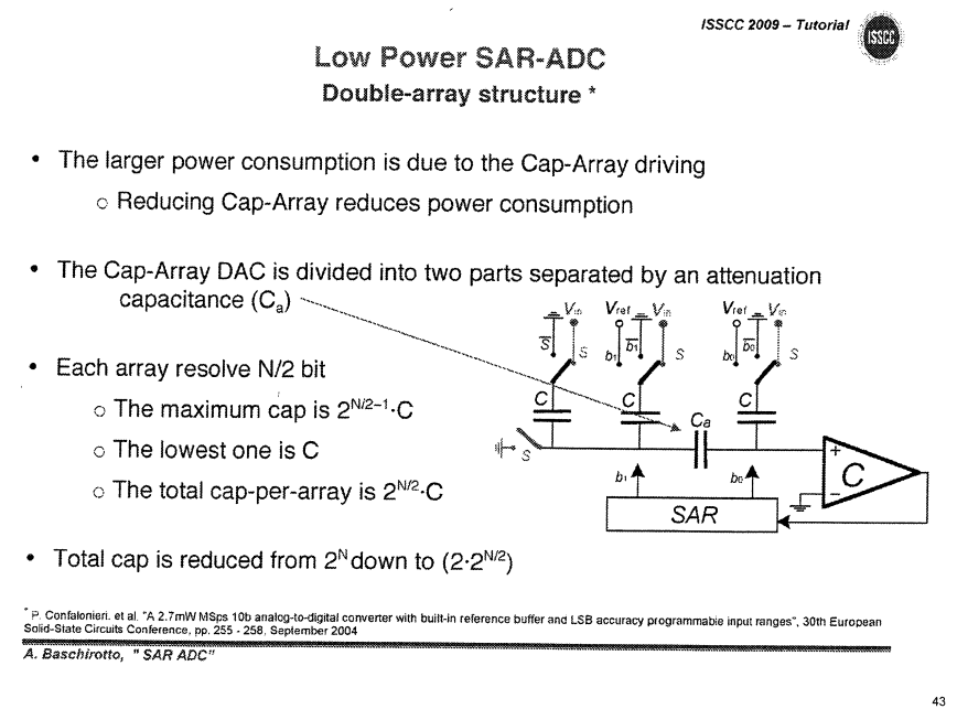
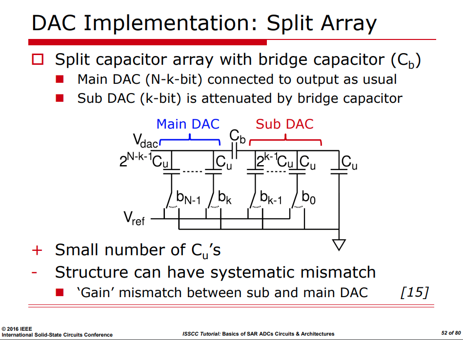
Split Arrary CDAC
Split capacitor, double-array cap
attenuation capacitance \(C_a\)

\[\begin{align} \Delta V_{dac} &= \frac{1}{2}b_3+\frac{1}{4}b_2+\frac{1}{4}\left(\frac{1}{2}b_1+\frac{1}{4}b_0 \right) \\ &= \frac{1}{2}b_3+\frac{1}{4}b_2 + \frac{1}{8}b_1+\frac{1}{16}b_0 \end{align}\]
Asynchronous processing
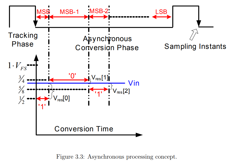
a global clock running at the sample rate is still used for an uniform sampling
The concept of asynchronous processing is to trigger the internal comparison from MSB to LSB like dominoes.
reference
S. -W. M. Chen and R. W. Brodersen, "A 6-bit 600-MS/s 5.3-mW Asynchronous ADC in 0.13-μm CMOS," in IEEE Journal of Solid-State Circuits, vol. 41, no. 12, pp. 2669-2680, Dec. 2006
Shuo-Wei Chen, Power Efficient System and A/D Converter Design for Ultra-Wideband Radio [http://www2.eecs.berkeley.edu/Pubs/TechRpts/2006/EECS-2006-71.pdf]
Andrea Baschirotto, "T6: SAR ADCs" ISSCC2009
Pieter Harpe, ISSCC 2016 Tutorial: "Basics of SAR ADCs Circuits & Architectures"