Analog Front-End (AFE)
Push-Pull
TODO 📅
Rinaldo Castello, "LINEARIZATION TECHNIQUES FOR PUSH-PULL AMPLIFIERS" [https://www.ieeetoronto.ca/wp-content/uploads/2020/06/AMPLIFIERS_Stanf_Tor_2016_Last.pdf]
Noise and Distortion
TODO 📅
Ali Sheikholeslami, University of Toronto, A-SSCC 2024 Circuit Insights:FT1 Noise and Distortion [link]
Response Speed in Analog Circuits
Hyun-Sik Kim, KAIST, A-SSCC 2024 Circuit Insights: FT3 Accelerating Response Speed in Analog Circuits [link]
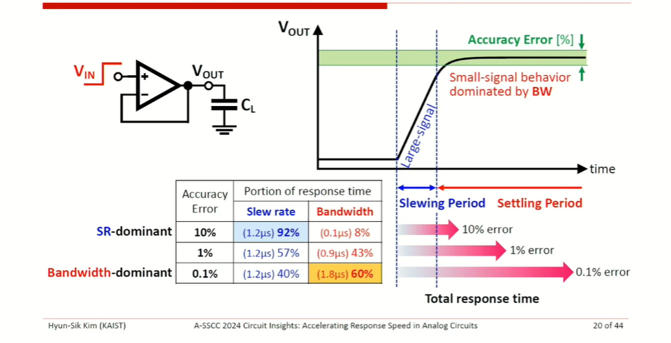
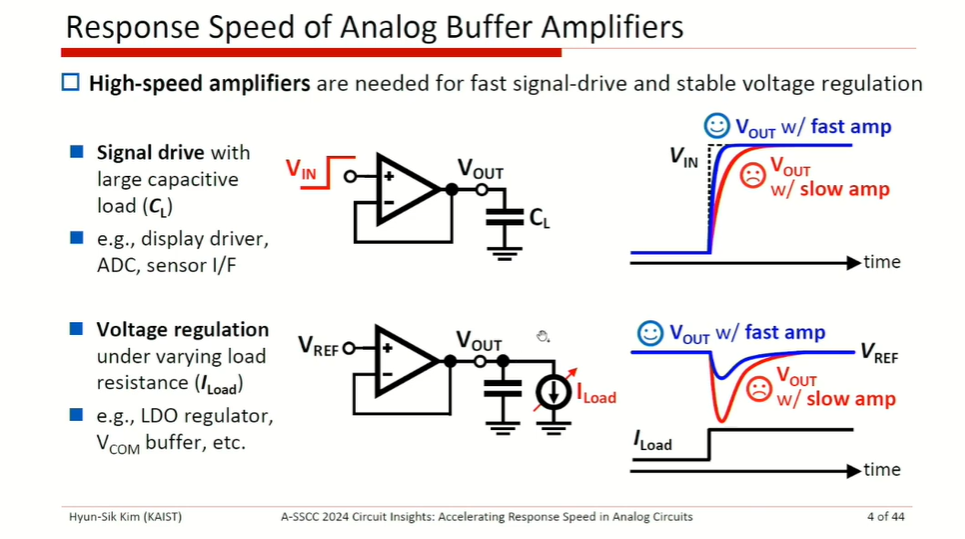
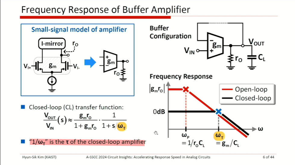
Bandwidth limitation
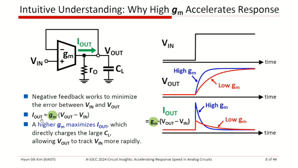
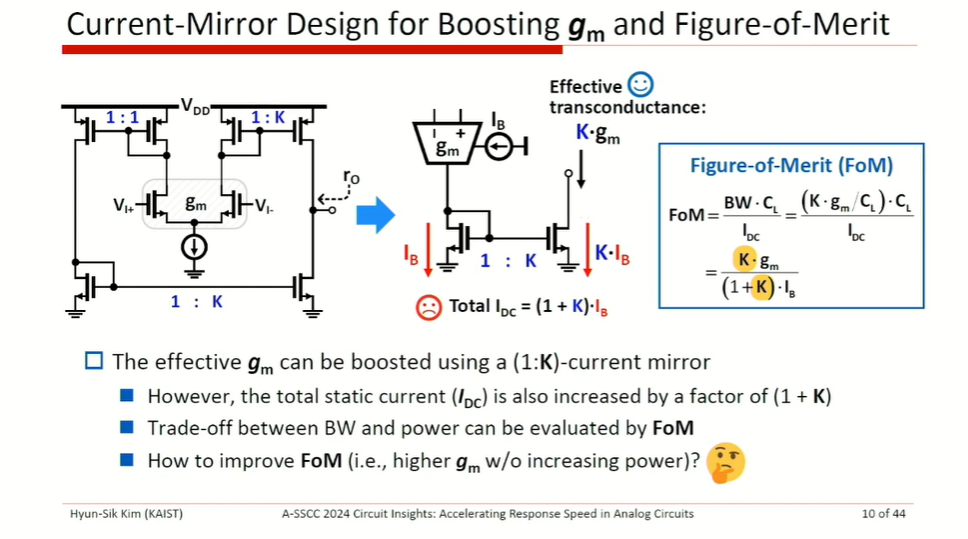

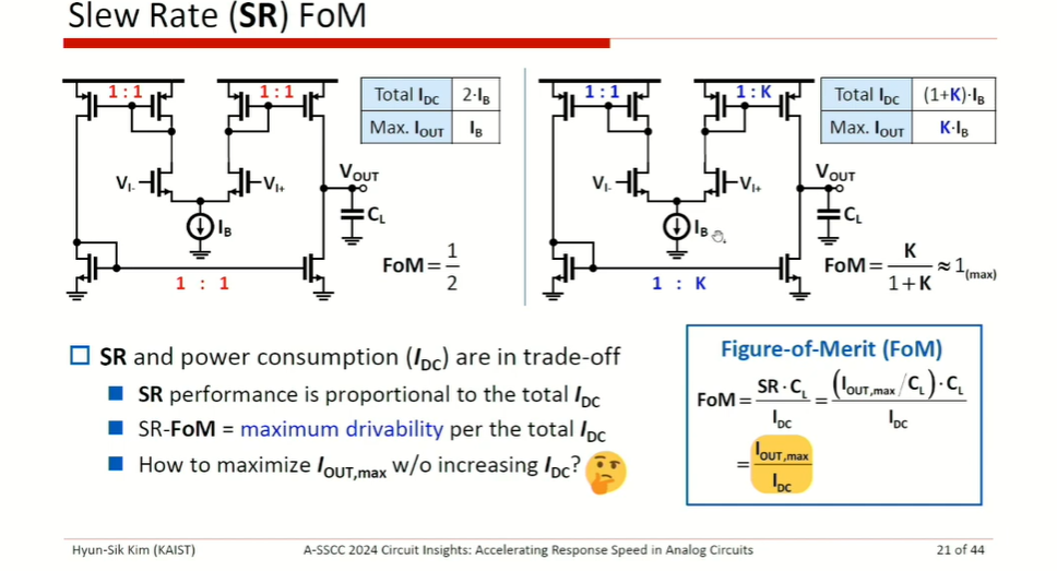
slew rate limitation
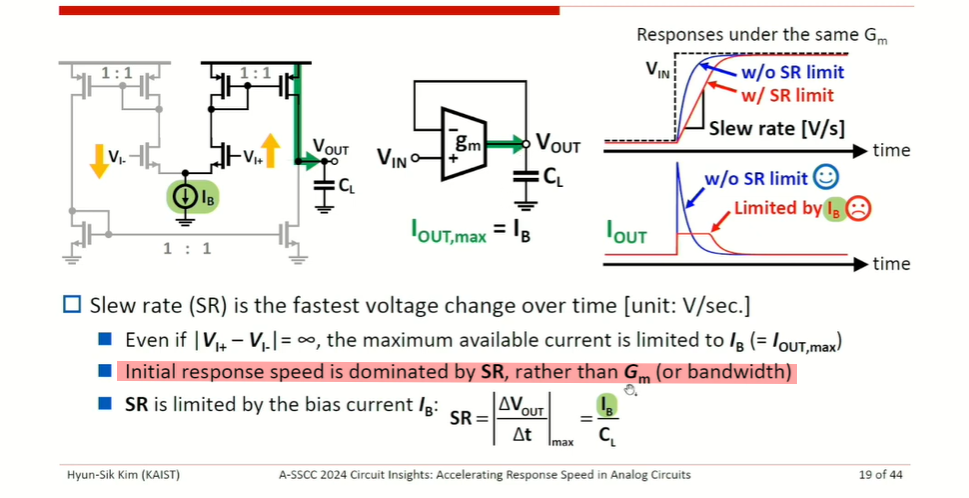
Assuming linear response \[ V_o(t) = 1 - e^{-\omega_T t} \]
\[ \frac{dV_o}{dt} = \omega_Te^{-\omega_T t} = \frac{g_m}{C_L}e^{-\omega_T t} = \frac{g_m}{I_B}\cdot \frac{I_B}{C_L}\cdot e^{-\omega_T t} \gt \frac{I_B}{C_L} \]
where \(\frac{g_m}{I_B} e^{-\omega_T t} \gt 1\) at initial response
Therefore, initial response speed is dominated by SR, rather than \(G_m\) (or bandwidth)
MOS parasitic Rd&Rs, Cd&Cs
Decrease the parasitic R&C
priority: \(R_s \gt R_d\), \(C_s \gt C_d\)
XCP as Negative Impedance Converter (NIC)
The Cross-Coupled Pair (XCP) can operate as an impedance negator [a.k.a. a negative impedance converter (NIC)]
A common application is to create a negative capacitance that can cancel the positive capacitance seen at a port, thereby improving the speed
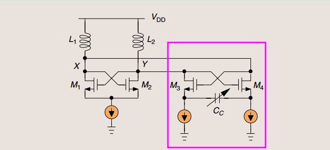 \[
I_{NIC} =\frac{V_{im} - V_{ip}}{\frac{2}{g_m}+\frac{1}{sC_c}} =
\frac{-2V_{ip}}{\frac{2}{g_m}+\frac{1}{sC_c}}
\] Therefore \[
Z_{NIC} = \frac{V_{ip} - V_{im}}{I_{NIC}}=\frac{2V_{ip}}{I_{NIC}} =-
\frac{2}{g_m}-\frac{1}{sC_c}
\] half-circuit
If \(C_{gd}\) is considered, and apply miller effect. half equivalent circuit is shown as below
B. Razavi, "The Cross-Coupled Pair - Part III [A Circuit for All Seasons]," IEEE Solid-State Circuits Magazine, Issue. 1, pp. 10-13, Winter 2015. [https://www.seas.ucla.edu/brweb/papers/Journals/BR_Magzine3.pdf]
S. Galal and B. Razavi, "10-Gb/s Limiting Amplifier and Laser/Modulator Driver in 0.18um CMOS Technology,” IEEE Journal of Solid-State Circuits, vol. 38, pp. 2138-2146, Dec. 2003. [https://www.seas.ucla.edu/brweb/papers/Journals/G&RDec03_2.pdf]
source follower
A. Sheikholeslami, "Voltage Follower, Part III [Circuit Intuitions]," in IEEE Solid-State Circuits Magazine, vol. 15, no. 2, pp. 14-26, Spring 2023, doi: 10.1109/MSSC.2023.3269457
—, ESSCIRC2023 Circuit Insights [https://youtu.be/2xFIZM5_FPw?si=536cMdIXyIny27Uk]
—, CICC2025 Circuit Insights: From Simple to Super Source Follower [https://youtu.be/CWfMKltPIQ8?si=s0npv2GSQKYBv513]
Paul R. Gray. 2009. Analysis and Design of Analog Integrated Circuits (5th. ed.). Wiley Publishing. [pdf]
Super-source follower (SSF)
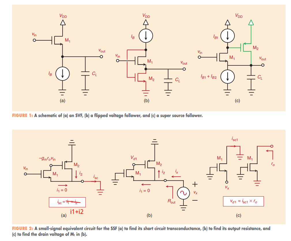


Flipped Voltage Follower (FVF)
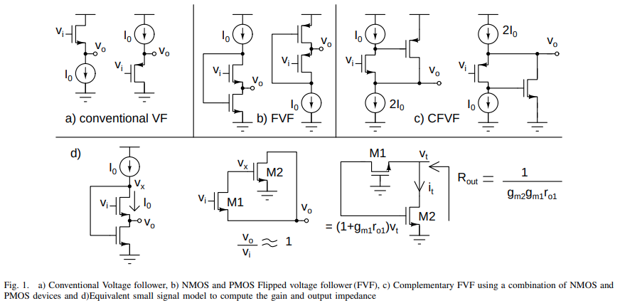
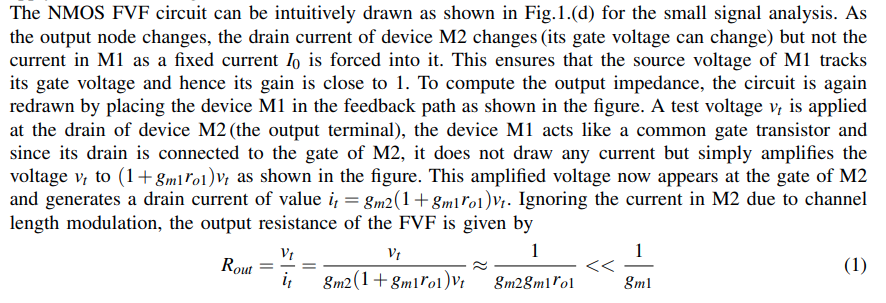
T&H buffer in ADC
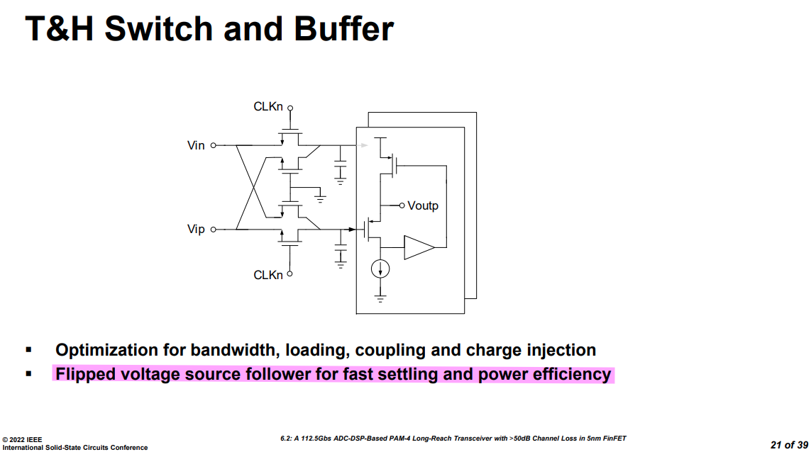
Z. Guo et al., "A 112.5Gb/s ADC-DSP-Based PAM-4 Long-Reach Transceiver with >50dB Channel Loss in 5nm FinFET," 2022 IEEE International Solid-State Circuits Conference (ISSCC), San Francisco, CA, USA, 2022, pp. 116-118, doi: 10.1109/ISSCC42614.2022.9731650.
Double differential Pair
\(V_\text{ip}\) and \(V_\text{im}\) are input, \(V_\text{rp}\) and \(V_\text{rm}\) are reference voltage \[ V_o = A_v(\overline{V_\text{ip} - V_\text{im}} - \overline{V_\text{rp} - V_\text{rm}}) \]
In differential comparison mode, the feedback loop ensure \(V_\text{ip} = V_\text{rp}\), \(V_\text{im} = V_\text{rm}\) in the end
assume input and reference common voltage are same
Pros of (b)
- larger input range i.e., \(\gt \pm \sqrt{2}V_\text{ov}\) of (a), it works even one differential is off due to lower voltage
- larger \(g_m\) (smaller input difference of pair)
Cons of (b)
- sensitive to the difference of common voltage between \(V_\text{ip}\), \(V_\text{im}\) and \(V_\text{rp}\), \(V_\text{rm}\)
common-mode voltage difference
copy aforementioned formula here for convenience \[ V_o = A_v(\overline{V_\text{ip} - V_\text{im}} - \overline{V_\text{rp} - V_\text{rm}}) \]
at sample phase \(V_\text{ip}= V_\text{im}= V_\text{cmi}\) and \(V_\text{rp}= V_\text{rm}= V_\text{cmr}\)
- \(I_\text{ip0}= I_\text{im0} = I_\text{i0}\)
- \(I_\text{rp0}= I_\text{rm0} = I_\text{r0}\)
i.e. \(\overline{I_\text{ip} + I_\text{rm}} - \overline{I_\text{im} + I_\text{rp}} = 0\)
at compare start
\(V_\text{ip}= V_\text{im}= V_\text{cmi}\) and \(V_\text{rp}= V_\text{cmr}+\Delta\), \(V_\text{rp}= V_\text{cmr}-\Delta\)
\(I_\text{ip}\lt I_\text{ip0}\), \(I_\text{rp} \gt I_\text{rp0}\)
\(I_\text{im}\gt I_\text{im0}\), \(I_\text{rm} \lt I_\text{rm0}\)
i.e. \(\overline{I_\text{ip} + I_\text{rm}} - \overline{I_\text{im} + I_\text{rp}} \lt 0\), we need to increase \(V_\text{ip}\) and decrease \(V_\text{im}\).
at the compare finish
\[\begin{align} V_\text{ip}= V_\text{cmi} + \Delta \\ V_\text{im}= V_\text{cmi} - \Delta \end{align}\]
and \(I_\text{ip0}= I_\text{im0} = I_\text{i0}\), \(I_\text{rp0}= I_\text{rm0} = I_\text{r0}\)
i.e. \(\overline{I_\text{ip} + I_\text{rm}} - \overline{I_\text{im} + I_\text{rp}} = 0\)
If \(V_\text{cmr} - V_\text{cmi} = \sqrt{2}V_{OV} + \delta\), and \(\delta \gt 0\). one transistor carries the entire tail current
- \(I_\text{ip} =0\) and \(I_\text{rp} = I_{SS}\), all the time
At the end, \(V_\text{im} = V_\text{cmi} - (\Delta - \delta)\), the error is \(\delta\)
In closing, \(V_\text{cmr} - V_\text{cmi} \lt \sqrt{2}V_{OV}\) for normal work
Furthermore, the difference between \(V_\text{cmr}\) and \(V_\text{cmi}\) should be minimized due to limited impedance of current source and input pair offset
In the end \[ V_\text{cmr} - V_\text{cmi} \lt \sqrt{2}V_{OV} - V_{OS} \]
Under the condition, every transistor of pairs are on in equilibrium
pair mismatch
\[\begin{align} I_{SE} &= g_m(\sigma_{vth,0} + \sigma_{vth,1}) \\ I_{DE} &= g_m(\sigma_{vth,0} + \sigma_{vth,1}) \end{align}\]
The input equivalient offset voltage \[\begin{align} V_{os,SE} &= \frac{I_{SE}}{2g_m} = \frac{\sigma_{vth,0} + \sigma_{vth,1}}{2} \\ V_{os,DE} &= \frac{I_{DE}}{g_m} = \sigma_{vth,0} + \sigma_{vth,1} \end{align}\]
Then \[\begin{align} \sigma_{vos,SE} &= \sqrt{\frac{2\sigma_{vth}^2}{4}} = \frac{\sigma_{vth}}{\sqrt{2}} \\ \sigma_{vos,DE} &= \sqrt{2\sigma_{vth}^2} = \sqrt{2}\sigma_{vth} \end{align}\]
We obtain \[ \sigma_{vos,DE} = 2\sigma_{vos,SE} \]
peaking without inductor
TODO 📅
How to generate complex poles without inductor? [https://a2d2ic.wordpress.com/2020/02/19/basics-on-active-rc-low-pass-filters/]
Input Diff-Pair
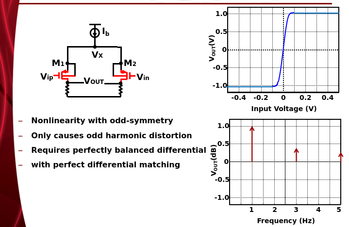
DM Distortion
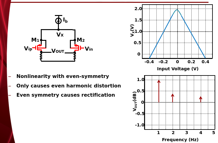
CM Distortion
Resistive Degeneration
Resistive degeneration in differential pairs serves as one major technique for linear amplifier
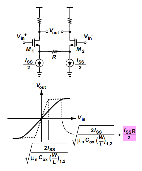
The linear region for CMOS differential pair would be extended by \(±I_{SS}R/2\) as all of \(I_{SS}/2\) flows through \(R\). \[\begin{align} V_{in}^+ -V_{in}^- &= V_{OV} + V_{TH}+\frac{I_{SS}}{2}R - V_{TH} \\ &= \sqrt{\frac{2I_{SS}}{\mu_nC_{OX}\frac{W}{L}}} + \frac{I_{SS}R}{2} \end{align}\]
Jri Lee, "Communication Integrated Circuits." https://cc.ee.ntu.edu.tw/~jrilee/publications/Comm_IC.pdf
Figure 14.12, Design of Analog CMOS Integrated Circuits, Second Edition [https://electrovolt.ir/wp-content/uploads/2014/08/Design-of-Analog-CMOS-Integrated-Circuit-2nd-Edition-ElectroVolt.ir_.pdf]
Biasing Tradeoffs in Resistive-Degenerated Diff Pair
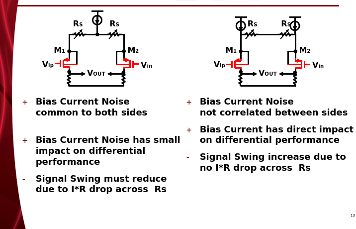
Todd Brooks, Broadcom "Input Programmable Gain Amplifier (PGA) Design for ADC Signal Conditioning" [https://classes.engr.oregonstate.edu/eecs/spring2021/ece627/Lecture%20Notes/OSU%20Classroom%20Presentaton%20042511.ppt]
Source-Degenerated Differential Pairs
TODO 📅
reference
Elad Alon, ISSCC 2014, "T6: Analog Front-End Design for Gb/s Wireline Receivers" [https://picture.iczhiku.com/resource/eetop/wHKfZPYpAleAKXBV.pdf]
Byungsub Kim, ISSCC 2022, "T11: Basics of Equalization Techniques: Channels, Equalization, and Circuits"
Minsoo Choi et al., "An Approximate Closed-Form Channel Model for Diverse Interconnect Applications," IEEE Transactions on Circuits and Systems-I: Regular Papers, vol. 61, no. 10, pp. 3034-3043, Oct. 2014.
K. Yadav, P. -H. Hsieh and A. Chan Carusone, "Linearity Analysis of Source-Degenerated Differential Pairs for Wireline Applications," in IEEE Open Journal of Circuits and Systems [https://ieeexplore.ieee.org/stamp/stamp.jsp?tp=&arnumber=10769573]