Digital Phase-Locked Loops
BB PD
Youngdon Choi, Deog-Kyoon Jeong and W. Kim, "Jitter transfer analysis of tracked oversampling techniques for multigigabit clock and data recovery," in IEEE Transactions on Circuits and Systems II: Analog and Digital Signal Processing, vol. 50, no. 11, pp. 775-783, Nov. 2003 [https://sci-hub.st/10.1109/TCSII.2003.819070]
John T. Stonick, ISSCC 2011 TUTORIALS T5: DPLL-Based Clock and Data Recovery
Walker, Richard. (2003). Designing Bang-Bang PLLs for Clock and Data Recovery in Serial Data Transmission Systems. [pdf]
—, Clock and Data Recovery for Serial Data Communications, focusing on bang-bang CDR design methodology, ISSCC Short Course, February 2002. [slides]
It's ternary, because early, late and no transition
notice the transition density = 1 in digital PLL
Linearization
The effective PD gain is a function of the input jitter pdf, it enables one to anticipate the effects of input jitter on loop characteristics
BB Gain is the slope of average BB output \(\mu\), versus phase offset \(\phi\), i.e. \(\frac {\partial \mu}{\partial \phi}\),
BB only produces output for a transition and this de-rates the gain. Transition density = 0.5 for random data
\[ K_{BB} = \frac{1}{2}\frac {\partial \mu}{\partial \phi} \]
where \(\mu = (1)\times \mathrm{P}(\text{late}|\phi) + (-1)\times \mathrm{P}(\text{early}|\phi)\)

Both jitter and amplitude noise distribution are same, just scaled by slope
Self-Noise Term
One price we pay for BB PD versus linear PD is the self-noise term. For small phase errors BB output noise is the full magnitude of the sliced data
The PD output should be almost 0 for small phase errors. i.e. ideal PD output noise should be 0
\[ \sigma_{BB}^2 = 1^2 \cdot \mathrm{P}(\text{trans}) + 0^2\cdot (1-\mathrm{P}(\text{trans})) = 0.5 \]

Input referred jitter from BB PD is proportional to incoming jitter
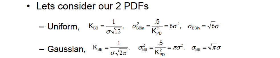
gain simulation
L. Avallone, M. Mercandelli, A. Santiccioli, M. P. Kennedy, S. Levantino and C. Samori, "A Comprehensive Phase Noise Analysis of Bang-Bang Digital PLLs," in IEEE Transactions on Circuits and Systems I: Regular Papers, vol. 68, no. 7, pp. 2775-2786, July 2021 [https://sci-hub.st/10.1109/TCSI.2021.3072344]
T. -K. Kuan and S. -I. Liu, "A Bang Bang Phase-Locked Loop Using Automatic Loop Gain Control and Loop Latency Reduction Techniques," in IEEE Journal of Solid-State Circuits, vol. 51, no. 4, pp. 821-831, April 2016 [https://sci-hub.st/10.1109/JSSC.2016.2519391]
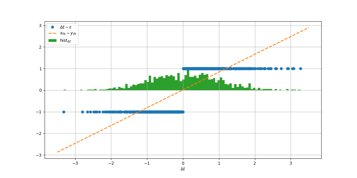
1 | import matplotlib.pyplot as plt |
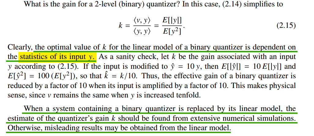
Pavan, Shanthi, Richard Schreier, and Gabor Temes. (2016). Understanding Delta-Sigma Data Converters. 2nd ed. Wiley. - 2.2.1 Quantizer Modeling
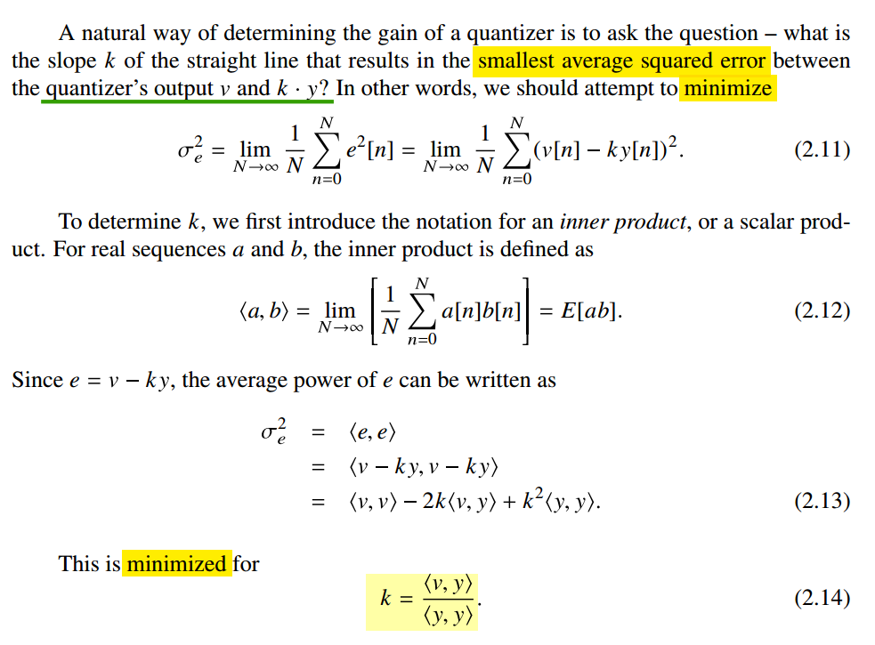 \[
\frac{\mathrm{d}\sigma_e^2}{\mathrm{d}k}
=0\space\space\Rightarrow\space\space
k=\frac{\left\langle v,y\right\rangle}{\left\langle y,y \right\rangle}
\]
\[
\frac{\mathrm{d}\sigma_e^2}{\mathrm{d}k}
=0\space\space\Rightarrow\space\space
k=\frac{\left\langle v,y\right\rangle}{\left\langle y,y \right\rangle}
\]
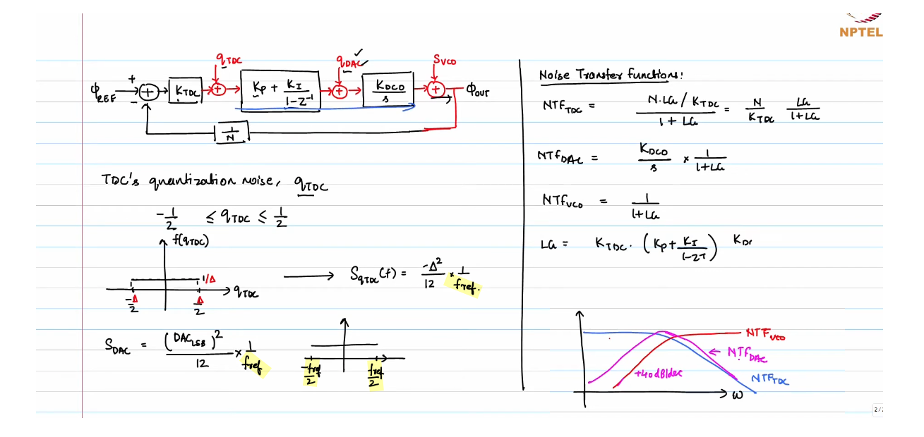
DCO Quantization Noise
TODO 📅
TDC Quantization Noise
TODO 📅
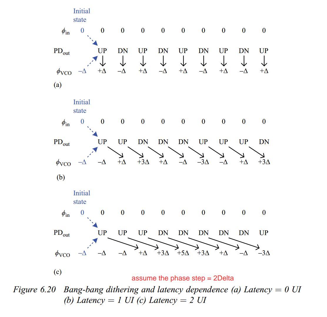
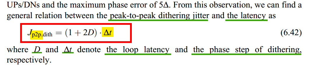
Hunting Jitter
S. Jang, S. Kim, S. -H. Chu, G. -S. Jeong, Y. Kim and D. -K. Jeong, "An Optimum Loop Gain Tracking All-Digital PLL Using Autocorrelation of Bang–Bang Phase-Frequency Detection," in IEEE Transactions on Circuits and Systems II: Express Briefs, vol. 62, no. 9, pp. 836-840, Sept. 2015 [https://sci-hub.st/10.1109/TCSII.2015.2435691] [phd thesis]
Deog-Kyoon Jeong. Topics in IC (Wireline Transceiver Design). Lec 3 - All-Digital PLL [https://ocw.snu.ac.kr/sites/default/files/NOTE/Lec%203%20-%20ADPLL.pdf]
—. Topics in IC (Wireline Transceiver Design). Lec 6 - Clock and Data Recovery [https://ocw.snu.ac.kr/sites/default/files/NOTE/Lec%206%20-%20Clock%20and%20Data%20Recovery.pdf]
Lee Hae-Chang.: ‘An estimation approach to clock and data recovery’, PhD Thesis, Stanford University, November 2006 [https://www-vlsi.stanford.edu/people/alum/pdf/0611_HaechangLee_Phase_Estimation.pdf]
J. Kim, Design of CMOS Adaptive-Supply Serial Links, Ph.D. Thesis, Stanford University, December 2002. [https://vlsiweb.stanford.edu/people/alum/pdf/0212_Kim_______Design_Of_CMOS_AdaptiveSu.pdf)]
High-speed Serial Interface 2013. Lect. 16 – Clock and Data Recovery 3 [http://tera.yonsei.ac.kr/class/2013_1_2/lecture/Lect16_CDR-3.pdf]
CC Chen. Why Hunting Jitter Happens in CDR: The Role of Input Jitter and Latency? [https://youtu.be/hPDielPsFgY]
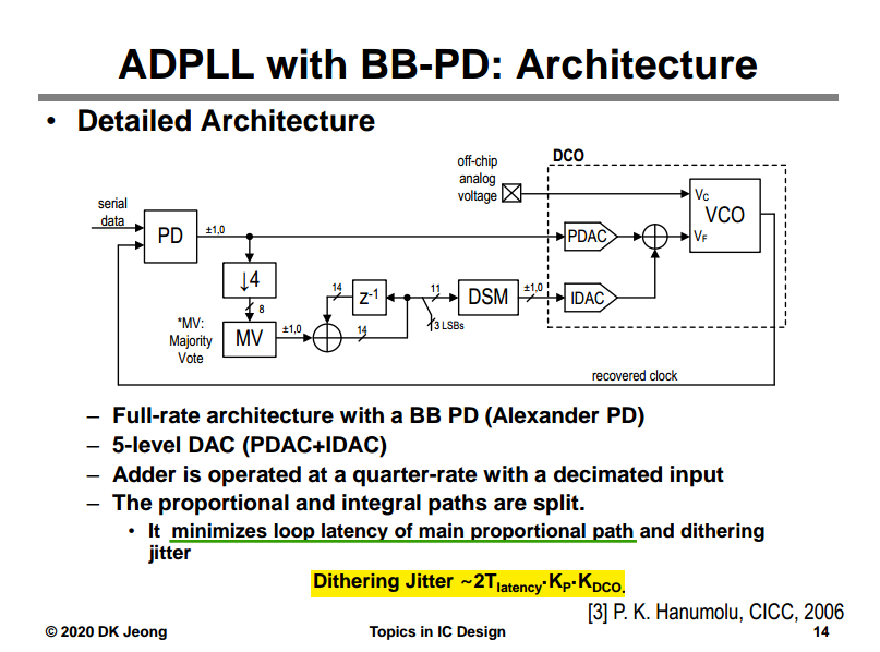
Hunting jitter is often referred to as dithering jitter, the periodic time error between data clock and input data, which exhibits a limit-cycle behavior
DT & CT Spectral Density
Sam Palermo, ECEN620: Network Theory Broadband Circuit Design Fall 2025 Lecture 9: Digital PLLs [https://people.engr.tamu.edu/spalermo/ecen620/lecture09_ee620_digital_PLLs.pdf]
Michael Perrott, August 14, 2008. Short Course On Phase-Locked Loops and Their Applications Day 4, AM Lecture Digital Frequency Synthesizers [https://www.cppsim.com/PLL_Lectures/day4_am.pdf]
—, "A modeling approach for Sigma Delta fractional-N frequency synthesizers allowing straightforward noise analysis," in IEEE Journal of Solid-State Circuits, vol. 37, no. 8, pp. 1028-1038, Aug. 2002 [https://www.cppsim.com/Publications/JNL/perrott_jssc02.pdf]
—. "Techniques for high data rate modulation and low power operation of fractional-N frequency synthesizers." 1997. [https://www.cppsim.com/Publications/Theses/perrott_phdthesis.pdf]
Hsu, Chun-Ming, Ph. D. Massachusetts Institute of Technology. "Techniques for high-performance digital frequency synthesis and phase control." 2008. [http://hdl.handle.net/1721.1/45870]
J. R. Barry, E. A. Lee, and D. G. Messerschmitt, Digital Communication, 3rd ed., Boston, MA: Kluwer Academic Publishers, 2003.

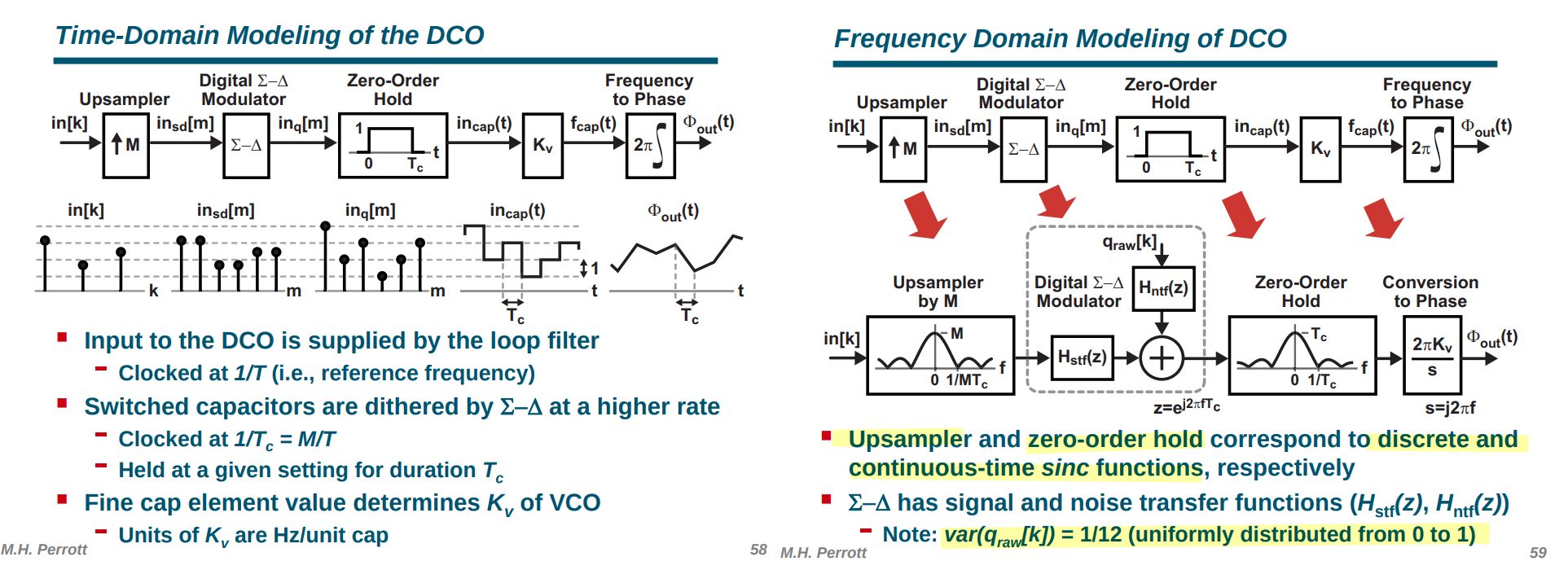
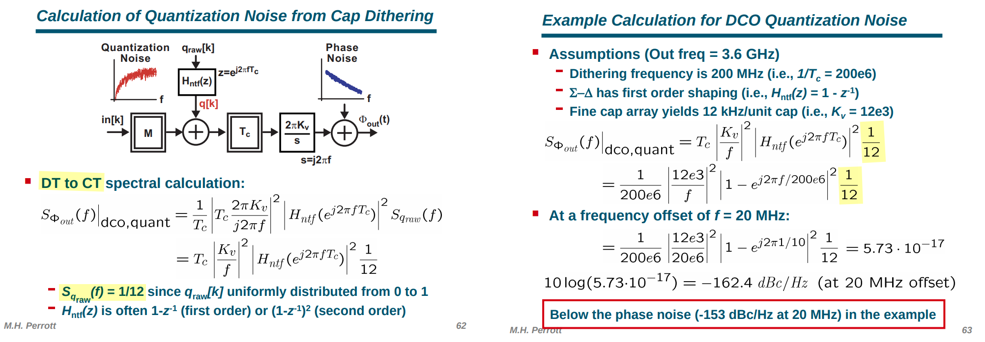
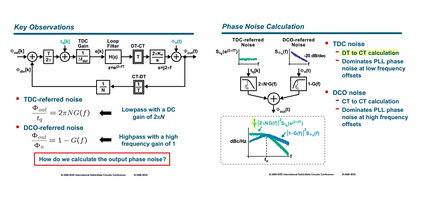
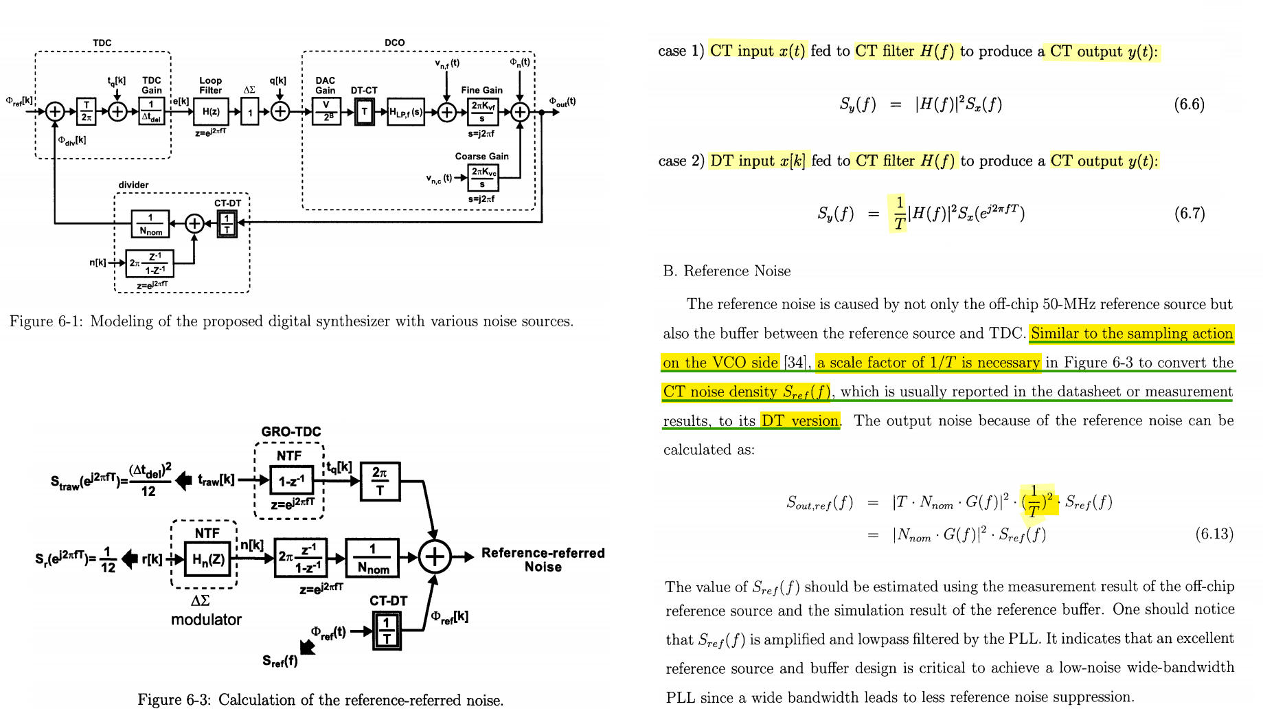
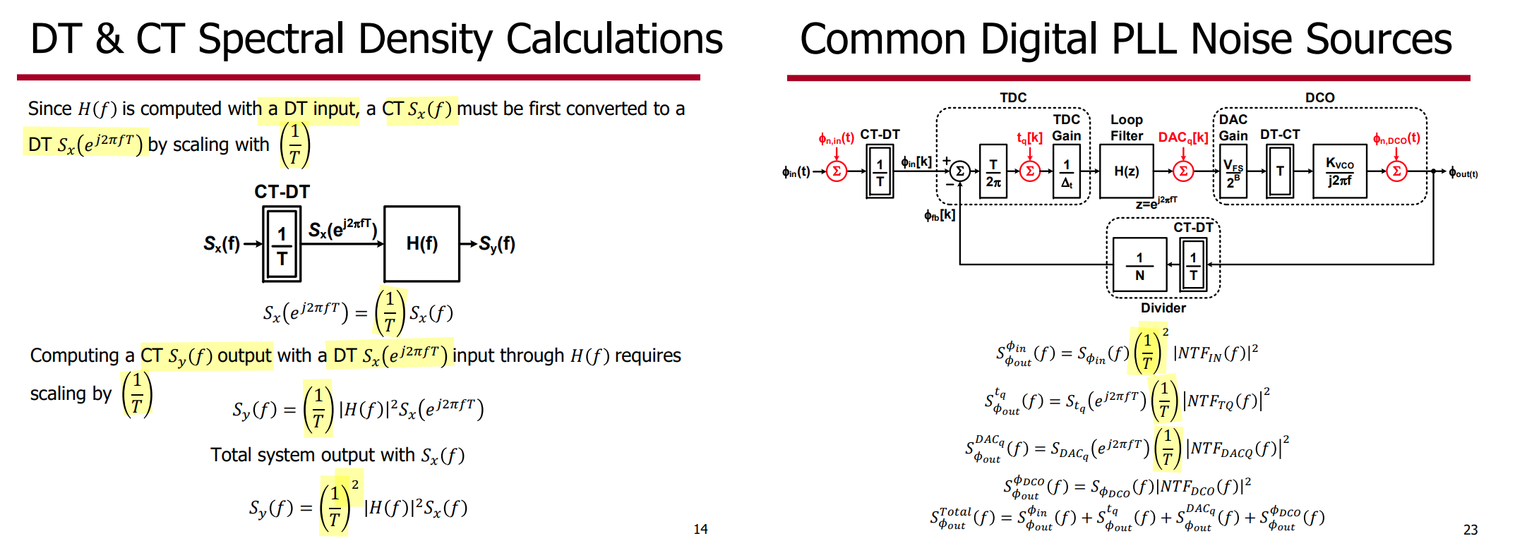
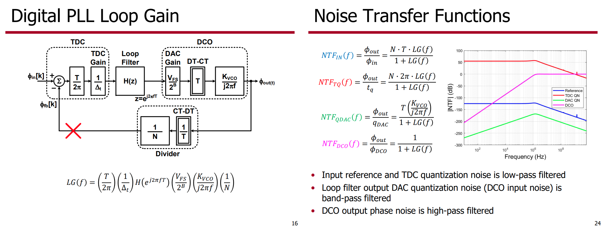
- \(\color{red}\frac{1}{T}\) of CT-DT originates from CT to sampled sequence to impulse train Fourier transform, which is explicit in frequency-domain model
- \(\color{red}\frac{1}{T}\) originates from DT spectrum to CT impulse spectrum is implicit in frequency-domain model
- \(\color{red}T\) of DT-CT originates from ZOH approximation following impulse train, which is explicit in frequency-domain model
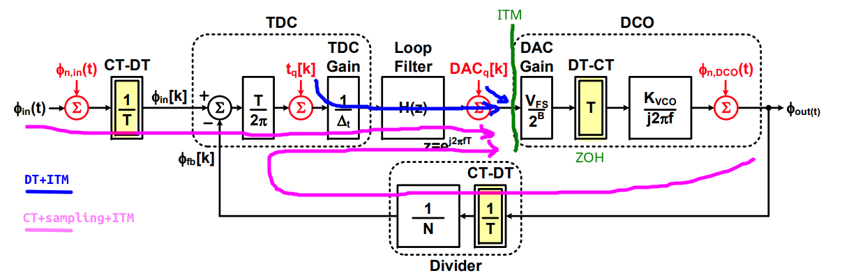
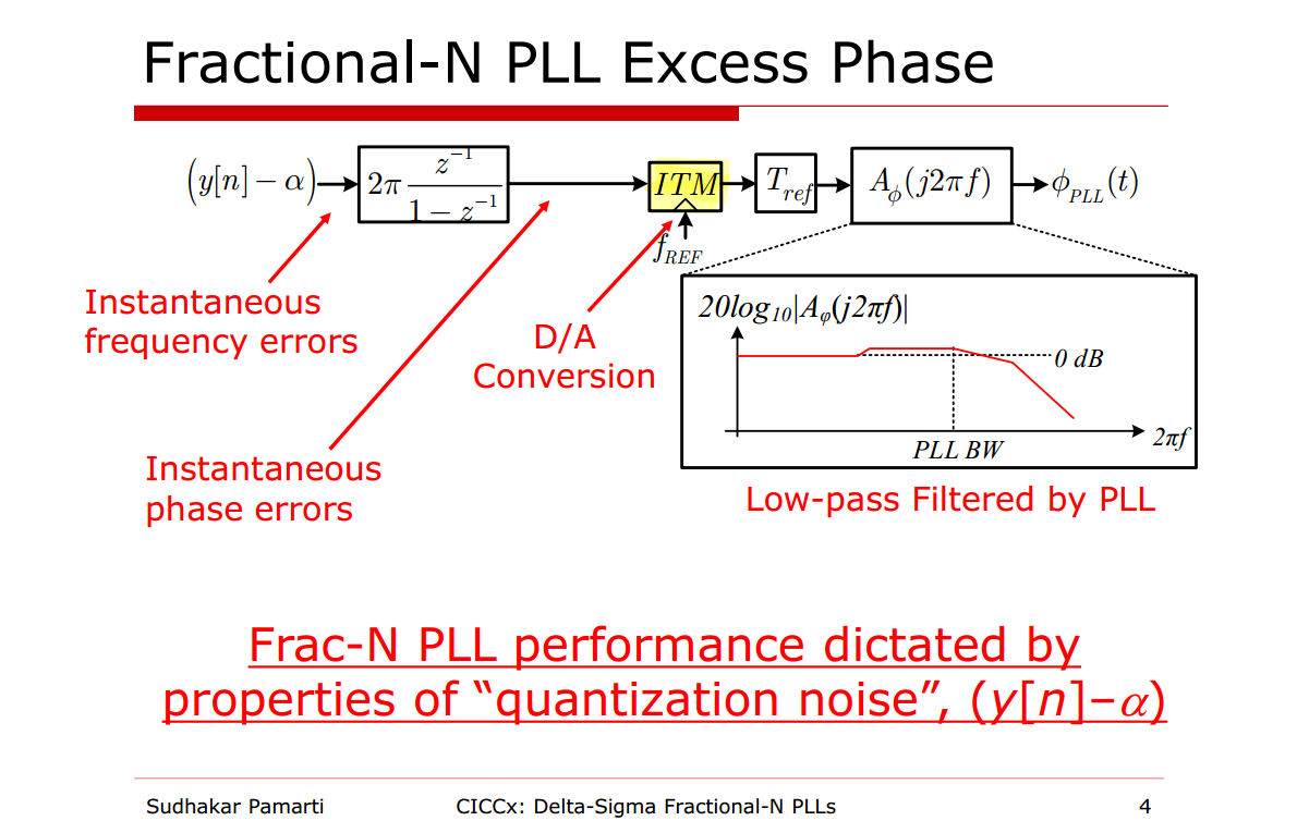
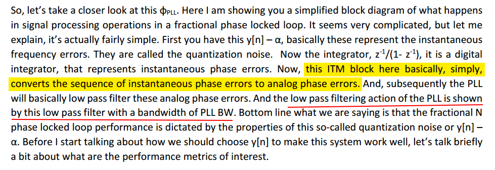
Divider Sampling Operation & ITM
Impulse Train Modulator (ITM)
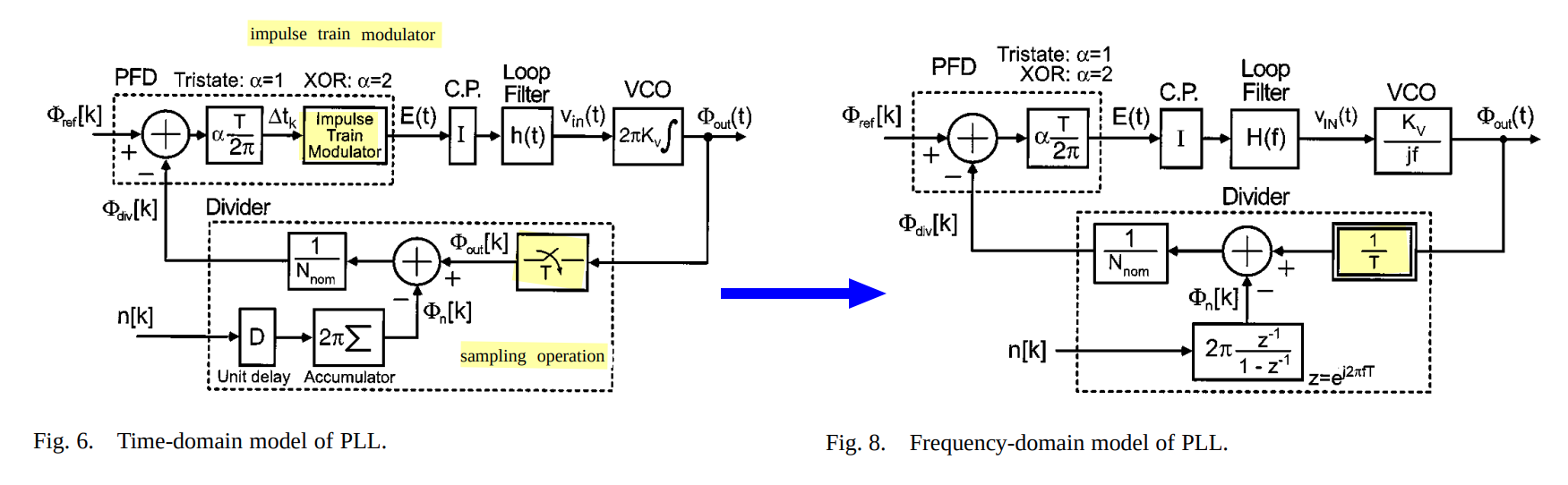
The double outline of the box in the figure is meant to serve as a reminder that a sampling operation is taking place
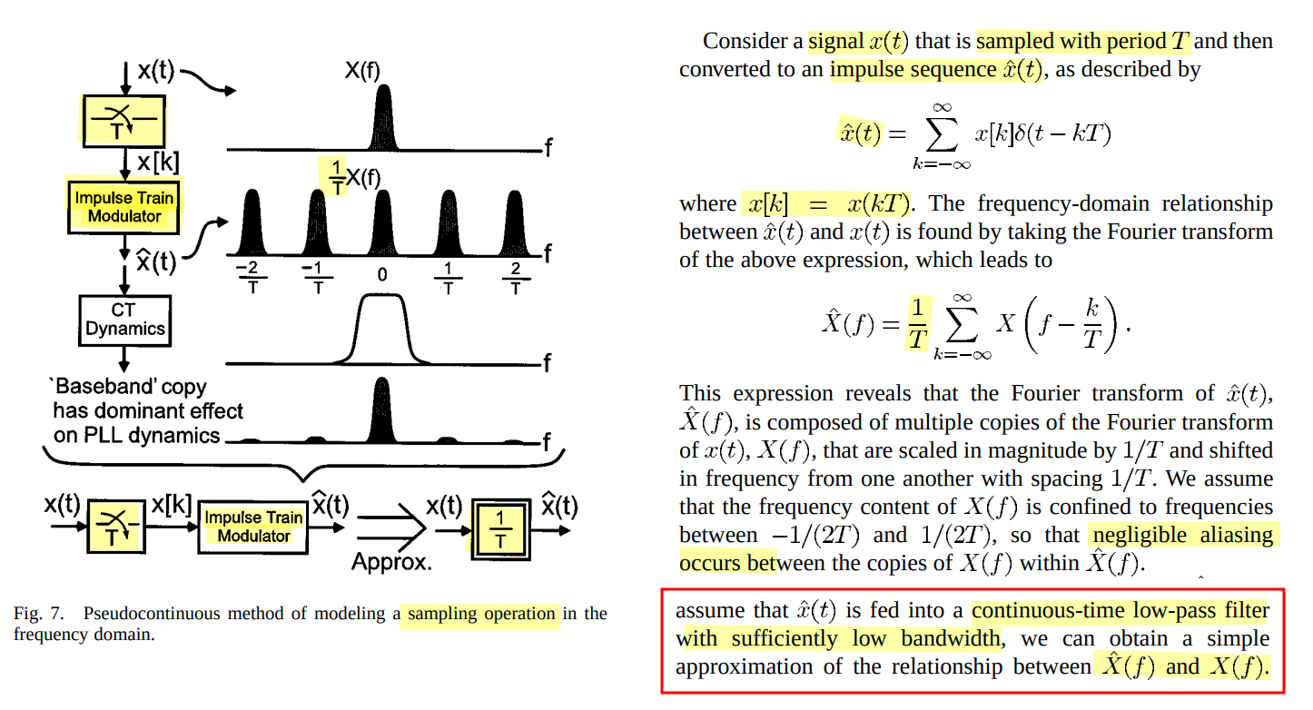
DT -> CT
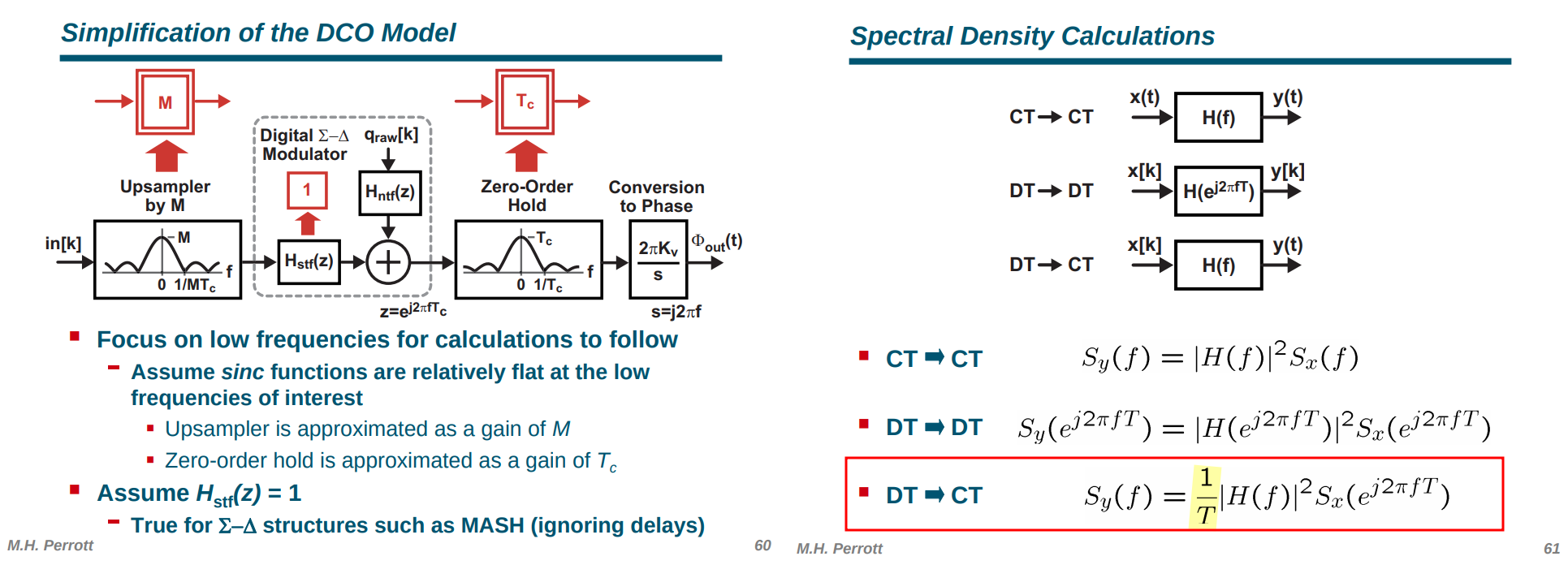
\(\boxed{S_x(e^{j2\pi fT}) = S_d(f)\cdot \textcolor{blue}{\frac{1}{T}}=S_c(f)\cdot \textcolor{blue}{\frac{1}{T}}}\), For example, the quantization noise spectrum is given by \(S_x(e^{j2\pi fT}) = \frac{1}{12f_s}\cdot \frac{1}{T} = \frac{1}{12}\). To convert the sequence spectrum into a continuous impulse train spectrum, we multiply by \(\color{blue}\frac{1}{T^2}\) \[ S_y(f) = S_x(e^{j2\pi fT}) \cdot \textcolor{blue}{T\cdot \frac{1}{T^2}\cdot |H(f)|^2 } = S_x(e^{j2\pi fT}) \cdot \textcolor{blue}{\frac{1}{T}|H(f)|^2} \]
CT -> DT -> CT
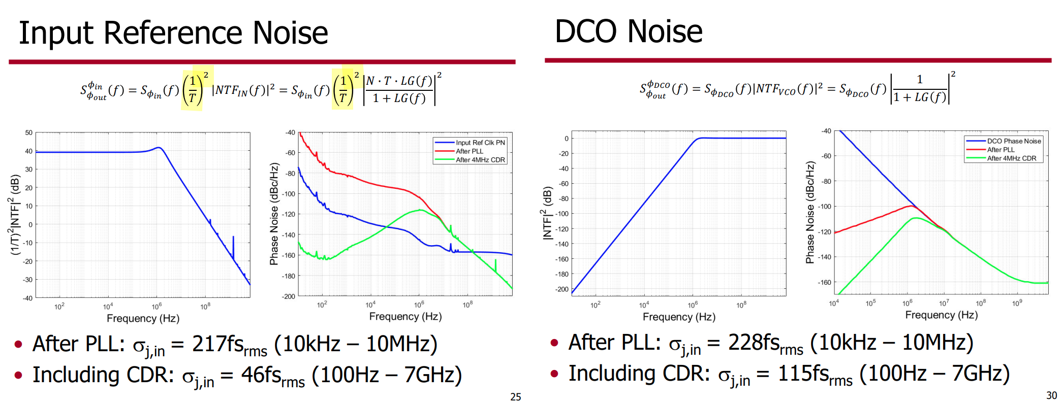
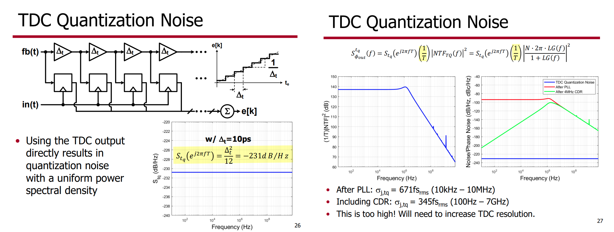
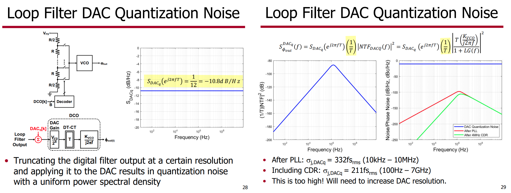
Assume that the lower \(m\) bits of the digital filter output are discarded by truncation. The truncation error is therefore modeled as a uniformly distributed random variable,
\[ E_t \sim U[0,2^m\text{LSB}] \]
Because the effective output resolution is reduced, the new least significant bit becomes
\[ \text{LSB}_t = 2^m\text{LSB} \]
and the DAC quantization error is correspondingly modeled as
\[ Q_{DAC} \sim U[0,1] \space \text{in}\space \text{LSB}_t \]
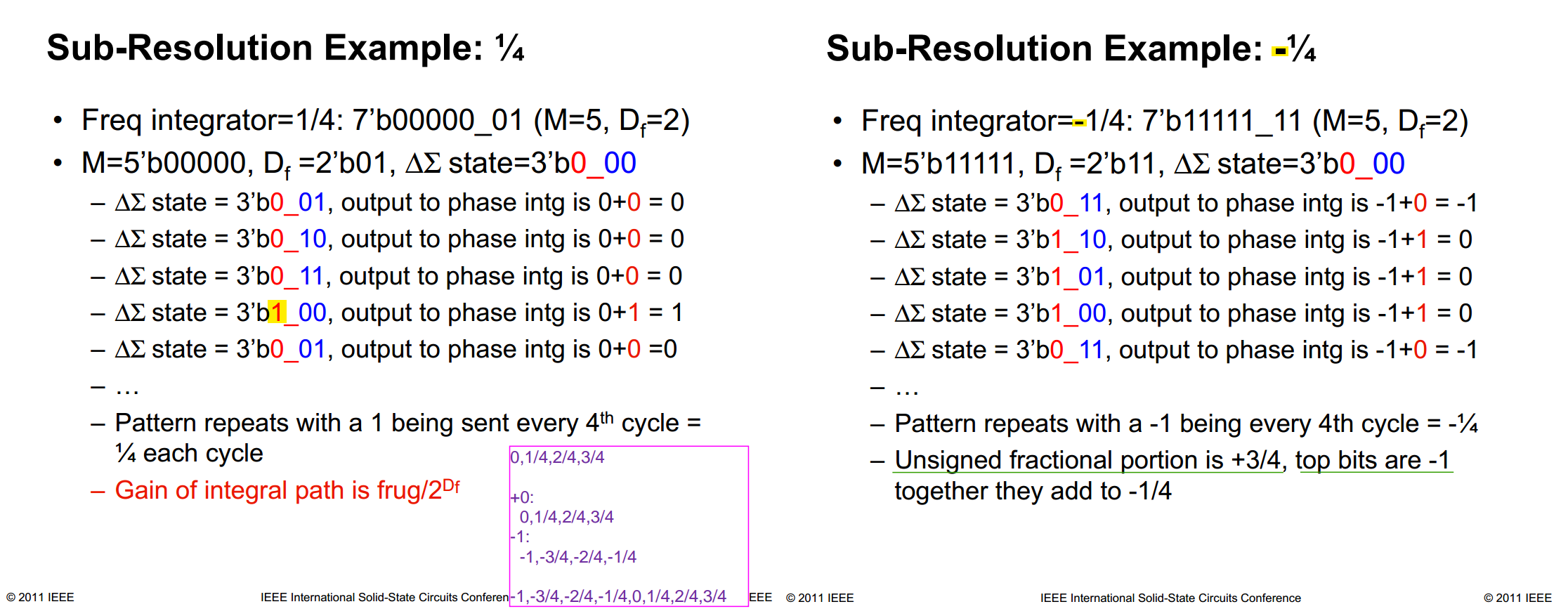
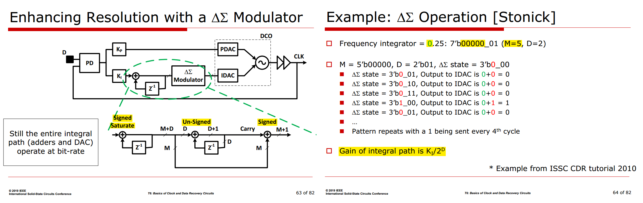
Enhancing Resolution w/ DSM
J. Stonick. ISSCC 2011 tutorials, T5: "DPLL-Based Clock and Data Recovery"
Amir Amirkhany. ISSCC 2019 "Basics of Clock and Data Recovery Circuits"
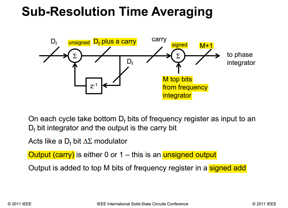
\(M+1\) bits ensure on overflow or underflow in the signed adder
MRDT (Multi-rate Discrete-Time) Modeling
Y. Hu, T. Siriburanon and R. B. Staszewski, "Multirate Timestamp Modeling for Ultralow-Jitter Frequency Synthesis: A Tutorial," in IEEE Transactions on Circuits and Systems II: Express Briefs, vol. 69, no. 7, pp. 3030-3036, July 2022 [https://ieeexplore.ieee.org/stamp/stamp.jsp?arnumber=9765581]
There are two key features associated with the behavior of DPLLs, namely, the multi-rate and discrete-time properties
reference & DCO model
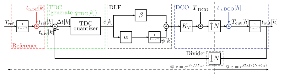
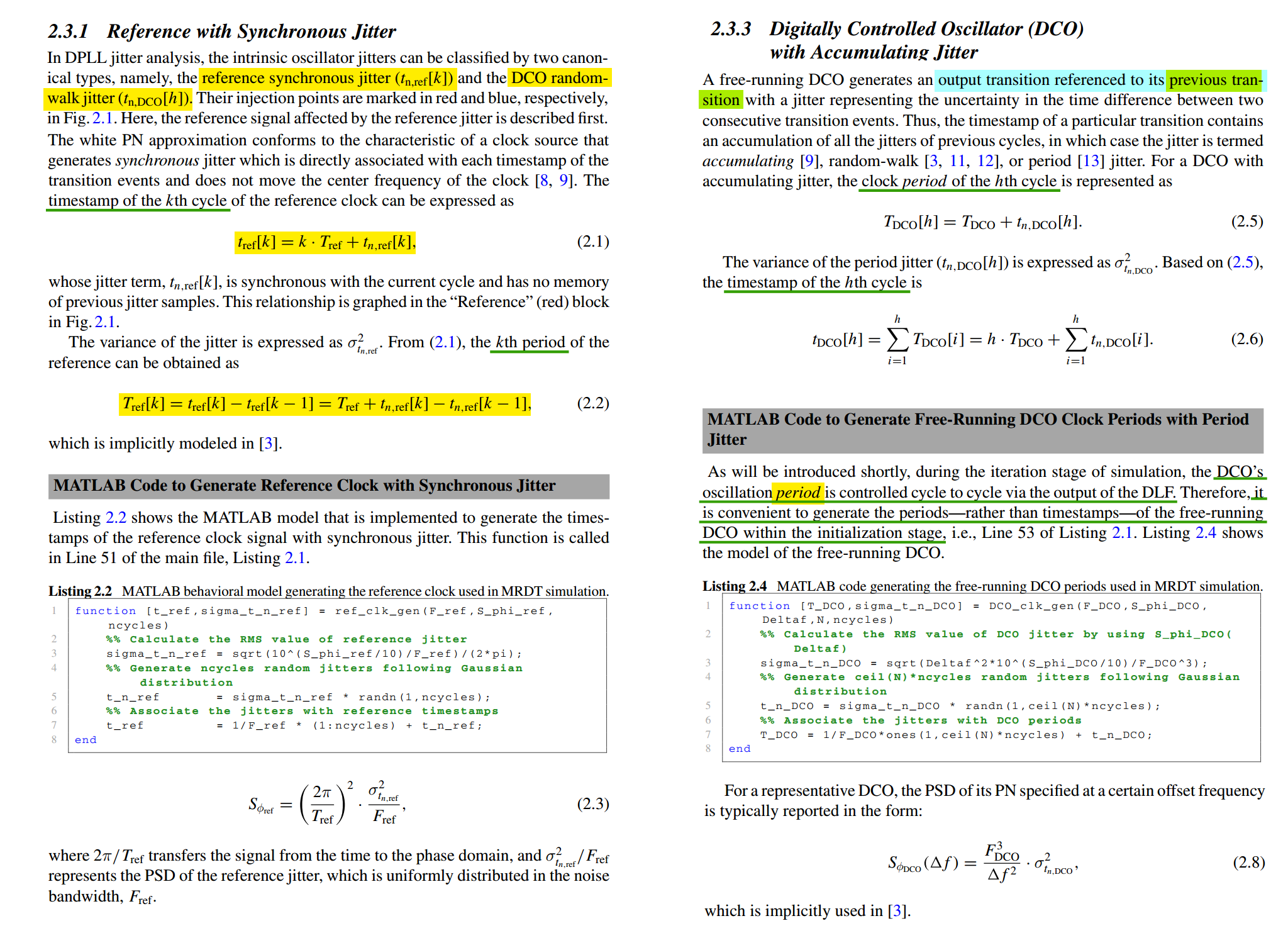
timestamps with synchronous jitter for reference clock signal
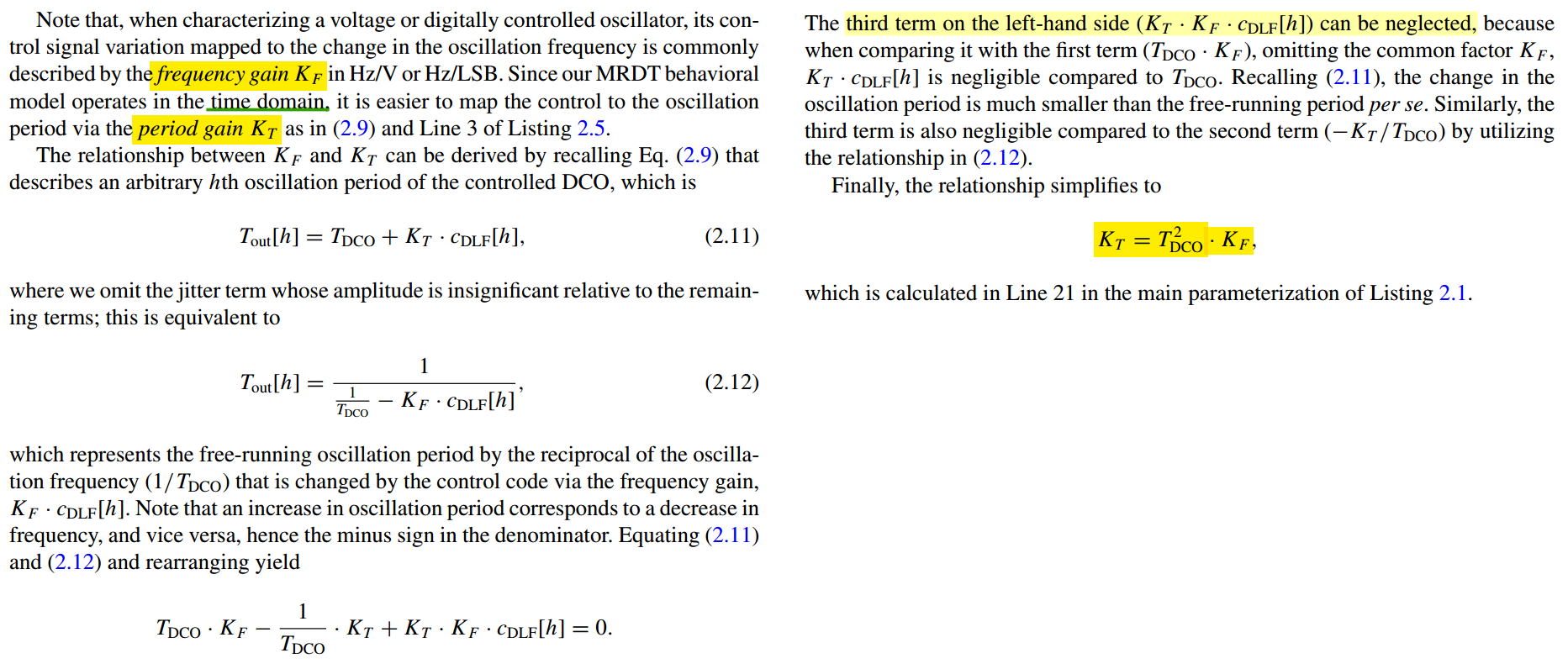
periods with period jitter for free-running DCO

output jitter, PN & input jitter
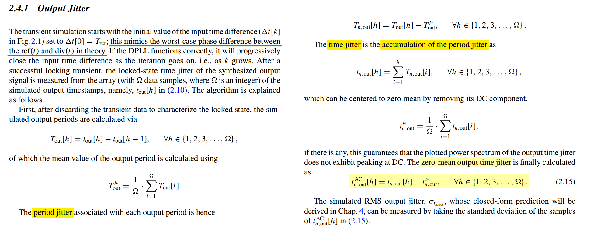
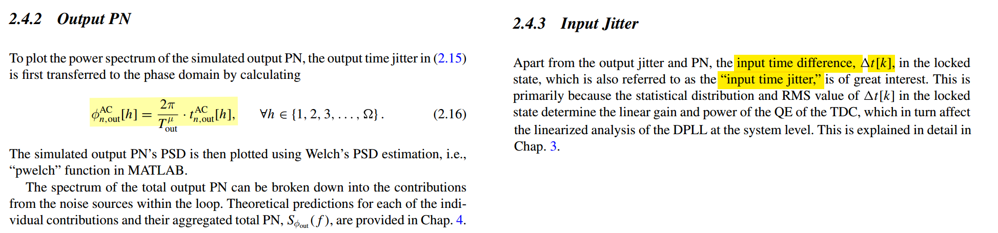
Determine quantitatively the system jitters and PN from behavioral simulation of the MRDT DPLL
1 | %% Wang, Xu and Michael Peter Kennedy. “Jitter and Spur Minimization in Fractional-N Digital Frequency Synthesizers - Modeling, Simulation, Analysis, and Design Methodologies.” *Analog Circuits and Signal Processing* (2026). |
cross-domain scaling for PSD-consistent
N. Da Dalt, "Linearized Analysis of a Digital Bang-Bang PLL and Its Validity Limits Applied to Jitter Transfer and Jitter Generation," in IEEE Transactions on Circuits and Systems I: Regular Papers, vol. 55, no. 11, pp. 3663-3675, Dec. 2008 [https://sci-hub.st/10.1109/TCSI.2008.925948]
—, “Theory and implementation of digital bang-bang frequency synthesizers for high speed serial data communications,” Ph.D. dissertation, RWTH Aachen University, Aachen, Germany, 2007. [https://publications.rwth-aachen.de/record/62439/files/DaDalt_Nicola.pdf]
H. Lu and P. P. Mercier, "Linear Periodically Time-Variant Digital PLL Phase Noise Modeling Using Conversion Matrices and Uncorrelated Upsampling," in IEEE Transactions on Circuits and Systems I: Regular Papers, vol. 71, no. 12, pp. 6021-6033, Dec. 2024, doi: 10.1109/TCSI.2024.3415001
At low frequencies, the transfer function from \(t_{r}\) to \(T_{v}\) can be approximated as: \[ H_{t_r,T_v} \approx \frac{1-z^{-1}}{Nz^{-1}} \]


\[ \boxed{ \text{For deriving Eq. (10), the }\uparrow N\text{ block must be treated as unity-amplitude rate conversion} } \]
The statement
\[ \uparrow N_{\text{Da Dalt}}=N\,\uparrow N_{\text{standard}} \]
cannot be inserted as a scalar gain \(N\) when deriving Eq. (10). If we do that, the explicit \(1/N\) in Fig. 10 cancels:
\[ N\times \frac1N=1 \]
and Eq. (10) would become \(N\) times larger. Its DC phase gain would then be \(N^2\), instead of the correct \(N\).
| \(H_{t_r,t_v}(1)\) | correct for | |
|---|---|---|
| without \(1/N\) | \(N\) | tracing waveforms, step responses |
| with \(1/N\) — Eq. (10) | \(1\) | PSD via (9), variance via (13) |
Da Dalt only ever uses the second. Hence the printed \(1/N\).
Equation (10) is never used to trace a waveform, while exists to be squared and multiplied into a spectrum, via (9):
\[ S_{\phi_v}(f) = \left|H_{\phi_r,\phi_v}(f)\right|^2\cdot\left(S_{\phi_r}+S_{\phi_{\mathrm{bpd}}}(f)\right) + \left|H_{\phi_{\mathrm{dco}},\phi_v}(f)\right|^2 S_{\phi_{\mathrm{dco}}}(f) \]
and to be integrated for jitter variance in (13). Both uses require a PSD-consistent transfer function, and for a slow-in/fast-out path that is not the same as the transform ratio.
Write the cross-domain path as
\[ y[n] = \sum_k h[n-kN]\,x[k] \]
with \(x\) zero-mean, white, and of variance \(\sigma^2\) on the slow grid \(T_{r0}\), and with real-valued \(h\). Then
\[ E\{y^2[n]\} = \sigma^2\sum_k h^2[n-kN] \]
The variance is \(N\)-periodic, but it need not differ between output phases. The output is generally cyclostationary; even when its variance is constant, its autocorrelation can depend on \(n\bmod N\).
Averaging the variance over \(N\) fast samples: \[ \overline{\sigma_y^2} = \frac{\sigma^2}{N}\sum_j h^2[j] \]
Now demand the ordinary form \[ S_y = c\,|H|^2 S_x \]
With the paper's convention \(S_x(f) = T_{r0}\sigma^2\), integrating over the fast Nyquist band \(F = N/T_{r0}\) and applying Parseval \(\int_{-F/2}^{F/2}|H|^2\,df = F\sum_j h^2[j]\):
\[ \overline{\sigma_y^2} = c\,T_{r0}\sigma^2\cdot\frac{N}{T_{r0}}\sum_j h^2[j] \quad\Longrightarrow\quad \textcolor{red}{c = \frac{1}{N^2}} \]
Finally
\[ \boxed{\;S_y(f) = \frac{|H|^2}{N^2}\,S_x(f)\;} \]
So the transfer function you may legitimately plug into \(S_y = |H|^2 S_x\) is \(\textcolor{red}{H/N}\), not \(H\). That is equation (10)
For the hold stage alone, \(H_{\mathrm{ZOH}}(z)=(1-z^{-N})/(1-z^{-1})\), whose impulse response is rectangular. For the complete cross-domain path, \(h\) denotes the full effective impulse response.
The root cause in one line: \(S_x\) is normalized on \(T_{r0}\) while \(S_y\) is normalized on \(T_{v0} = T_{r0}/N\). The \(1/N\) reconciles the two normalizations.

Assume real-valued \(h\) and zero-mean white input:
\[ E\{x[k]\}=0,\qquad E\{x[k]x[\ell]\}=\sigma^2\delta_{k\ell}. \]
Here \(k\) indexes slow samples, while \(n\) indexes fast samples; one slow interval contains \(N\) fast samples.
Starting from
\[ y[n]=\sum_k h[n-kN]x[k], \]
we have \(E\{y[n]\}=0\), so its variance equals its second moment. Expanding the square:
\[ \begin{aligned} \operatorname{Var}(y[n]) &=E\!\left\{ \left(\sum_k h[n-kN]x[k]\right) \left(\sum_\ell h[n-\ell N]x[\ell]\right) \right\}\\ &=\sum_k\sum_\ell h[n-kN]h[n-\ell N]\, E\{x[k]x[\ell]\}\\ &=\boxed{\sigma^2\sum_k h^2[n-kN]}. \end{aligned} \]
Every term with \(k\ne\ell\) vanishes because distinct input samples are uncorrelated. Independence is unnecessary.
Write \(n=qN+r\), where \(r\in\{0,\ldots,N-1\}\). Then
\[ \operatorname{Var}(y[qN+r]) =\sigma^2\sum_k h^2[r-(k-q)N] =\sigma^2\sum_m h^2[r-mN]. \]
The result depends only on the phase \(r\), not the period number \(q\).
Thus, at each output phase, the variance uses only the filter coefficients whose indices have that particular remainder modulo \(N\).
Take the arithmetic average of these \(N\) phase variances:
\[ \overline{\sigma_y^2} =\frac1N\sum_{r=0}^{N-1}\operatorname{Var}(y[r]) =\frac{\sigma^2}{N} \sum_{r=0}^{N-1}\sum_k h^2[r-kN]. \]
Every integer \(j\) has exactly one representation
\[ j=r-kN,\qquad 0\le r<N. \]
Consequently, the double sum includes every \(h^2[j]\) exactly once:
\[ \boxed{\overline{\sigma_y^2} =\frac{\sigma^2}{N}\sum_j h^2[j]}. \]
This is the average of the variances, not the variance of an averaged output signal.
\[ \boxed{\text{Physically: zero stuff }T_v\rightarrow\text{ZOH}\rightarrow\text{accumulate; no }1/N} \]
Because \(f_{\mathrm{mod}} = 1\,\mathrm{kHz}\) is near DC relative to the loop bandwidth, you should get approximately \[ j_v(t) \approx j_r(t) \]
and therefore
\[ \frac{A_{\mathrm{out}}}{A_{\mathrm{in}}} \approx 1 \]
or
\[ 20\log_{10}\left|\frac{J_v}{J_r}\right| \approx 0\,\mathrm{dB}. \]
Here \(J_v\) and \(J_r\) are the Fourier components of the output and reference timing jitter at \(f_{\mathrm{mod}}\).
At the same time,
\[ \Delta t = j_r - j_v \approx 0. \]
[Github Gist — dpll_in_out.py]
1 | # ============================================================ |
So, specifically for Python model:
\[ \boxed{ \texttt{np.repeat(x,N)} = \uparrow N+ \frac{1-z^{-N}}{1-z^{-1}} } \]
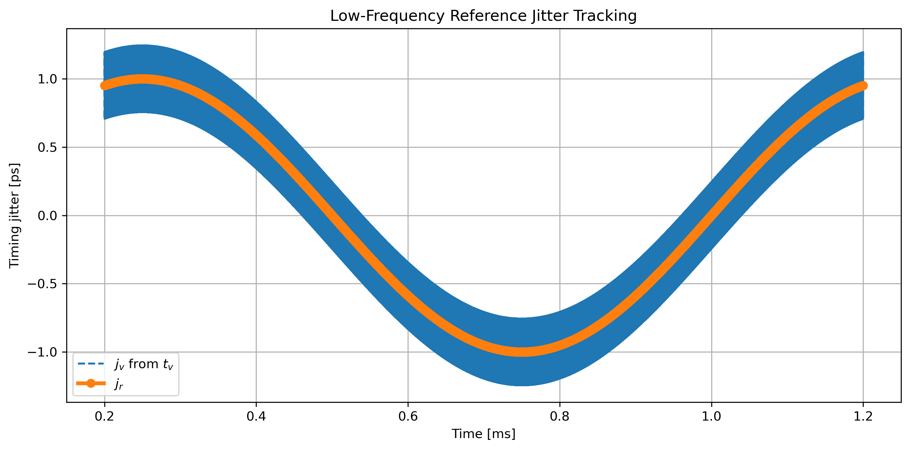
1 | ============================================================ |
!!DPLL time-domain model
L. Avallone, M. Mercandelli, A. Santiccioli, M. P. Kennedy, S. Levantino and C. Samori, "A Comprehensive Phase Noise Analysis of Bang-Bang Digital PLLs," in IEEE Transactions on Circuits and Systems I: Regular Papers, vol. 68, no. 7, pp. 2775-2786, July 2021 [https://sci-hub.st/10.1109/TCSI.2021.3072344]
—, “Contributions to the Theory and Development of Low-Jitter Bang-Bang Integrated Frequency Synthesizers.” University College Dublin. School of Electrical and Electronic Engineering, 2022. [http://hdl.handle.net/10197/13372]
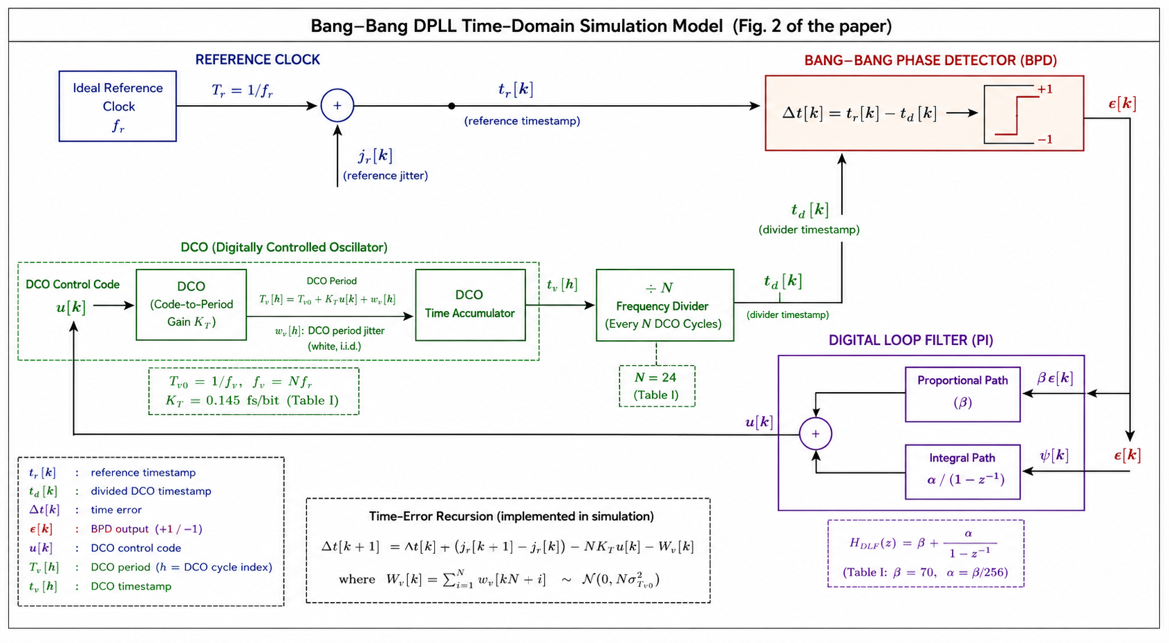
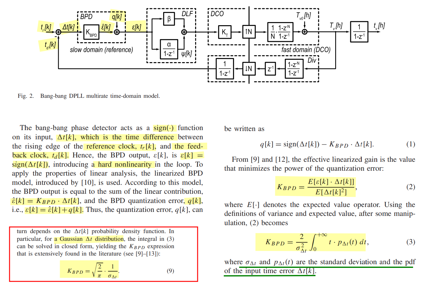
The paper defines the BPD input as
\[ \boxed{\Delta t[k]=t_r[k]-t_d[k]} \]
where \(t_r[k]\) is the reference-edge timestamp and \(t_d[k]\) is the divider-output timestamp.
The signal chain is essentially \[ \epsilon[k] \rightarrow \underbrace{\beta\epsilon[k]+\psi[k]}_{u[k]} \rightarrow \underbrace{K_T u[k]}_{\text{DCO period change}} \rightarrow T_v. \]
A useful distinction is that \(K_T\) is not the usual DCO frequency gain \(K_{\mathrm{DCO}}\) in Hz/code. This paper models the DCO in the period domain, so its gain is period/code. Around the nominal operating point, \(f=\frac{1}{T}\)
hence for a small period change,
\[ \Delta f \approx -\frac{\Delta T}{T_0^2}. \]
Therefore the corresponding frequency gain would be approximately
\[ \boxed{ K_{\mathrm{DCO}} \approx -\frac{K_T}{T_0^2} = -K_T f_v^2 } \]
in Hz/code. The minus sign means increasing the period lowers the frequency.

with \(t_A = t_B - d_t[k]=j_r[k]-d_t[k]\) \[ t_C = t_A + NT_{v0}+NK_T u[k]+W_v[k] = j_r[k]-d_t[k] + NT_{v0}+NK_T u[k]+W_v[k] \] with \(t_D = N T_{v0} + j_r[k+1]\) \[ \textcolor{red}{d_t[k+1]} = t_D - t_C = \textcolor{red}{\boxed{d_t[k] + (j_r[k+1] - j_r[k]) - NK_T u[k]-W_v[k]}} \]
1 | %% DPLL parameters from the paper |
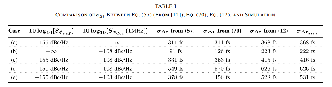
There are two different random sequences: \[ \boxed{j_r[k] = \text{absolute reference edge jitter}} \]
versus
\[ \boxed{\delta T_r[k]=j_r[k+1]-j_r[k] =\text{reference period jitter}}. \]
Our simulation generates
1 | jr = sigma_ref * randn(...); |
because the paper assumes white absolute reference jitter. The paper explicitly calls \(\sigma_{t_r}^2\) the absolute jitter variance of the reference.
Then the model naturally converts that absolute jitter into reference-period variation using
1 | jr(k+1) - jr(k) |
There is also a subtle but important consequence. If \(j_r[k]\sim\mathcal N(0,\sigma_{t_r}^2)\) is i.i.d., then \(\operatorname{Var}\{j_r[k+1]-j_r[k]\} = 2\sigma_{t_r}^2.\)
But consecutive period errors are correlated:
\[ \operatorname{Cov} \left( j_r[k+1]-j_r[k], j_r[k+2]-j_r[k+1] \right) = -\sigma_{t_r}^2. \]
So you should not replace the code with independent samples such as
1 | djr = sqrt(2)*sigma_ref*randn(...); |
because that gets the variance right but loses the required correlation.
In short:
\[ \boxed{ \texttt{jr[k]}=\text{edge jitter} \quad\Rightarrow\quad \texttt{jr[k+1]-jr[k]}=\text{period jitter} } \]
and the DPLL recursion evolves from one edge interval to the next, which is why the difference appears.
\(\boxed{\sigma_{\Delta t}}\) at the BPD input, not directly the RMS DCO-output jitter. To obtain actual DCO-output jitter, we should also simulate/store \(t_v[h]\), rather than only the reference-rate recursion for \(\Delta t[k]\).
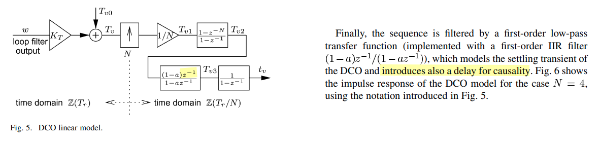
causality z-1 in linear model
\(\textcolor{red}{z^{-1}}\) makes the loop causal, and it represents the one-reference-cycle latency that is physically unavoidable in a digital PLL
With the indexing used in this slide,
\[ \boxed{\Delta t[k]=t_r[k]-t_v[k-1]} \]
so in the \(z\)-domain,
\[ \Delta T(z)=T_r(z)-z^{-1}T_v(z) \]
That is exactly the \(z^{-1}\) shown in the feedback path.
The timing sequence is essentially
\[ t_v[k-1] \;\longrightarrow\; \Delta t[k] \;\longrightarrow\; \text{TDC/filter} \;\longrightarrow\; u[k] \;\longrightarrow\; t_v[k] \]
Meanwhile the DCO timing recursion is
\[ t_v[k]=t_v[k-1]+N K_T u[k] \]
which gives
\[ \frac{T_v(z)}{U(z)} = \frac{N K_T}{1-z^{-1}} \]
So the two appearances of \(z^{-1}\) have related but different meanings:
- Inside \(\displaystyle \frac{NK_T}{1-z^{-1}}\): the DCO accumulates period/time increments.
- In the feedback path: the TDC at iteration \(k\) sees the previous DCO/divider timing state \(t_v[k-1]\).
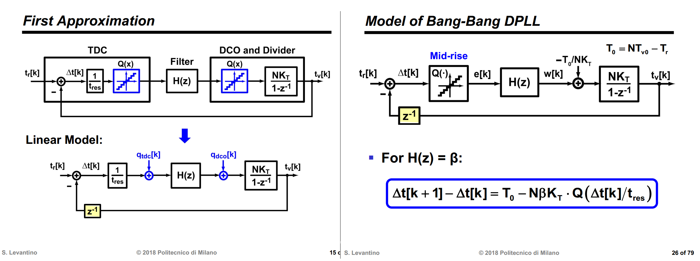
A useful way to read the lower figure is therefore:
\[ \boxed{ t_r[k] - \underbrace{t_v[k-1]}_{\text{available feedback edge}} \rightarrow \text{TDC} \rightarrow H(z) \rightarrow \text{DCO} \rightarrow t_v[k] } \]
Model at Reference Rate
S. Levantino, "Digital phase-locked loops," 2018 IEEE Custom Integrated Circuits Conference (CICC), San Diego, CA, USA, 2018
—, "Advanced digital phase-locked loops," Proceedings of the IEEE 2013 Custom Integrated Circuits Conference, San Jose, CA, USA, 2013, pp. 1-95 [https://sci-hub.jp/10.1109/CICC.2013.6658505]
 \[
\boxed{\frac{T_V}{W}(z) = \frac{NK_T}{z-1} =
\frac{NK_T}{\textcolor{red}{1-z^{-1}}}\cdot\textcolor{red}{z^{-1}}}
\]
\[
\boxed{\frac{T_V}{W}(z) = \frac{NK_T}{z-1} =
\frac{NK_T}{\textcolor{red}{1-z^{-1}}}\cdot\textcolor{red}{z^{-1}}}
\]

\[\begin{align} y[n] &= y[n-1] + x[n-1] \quad &\Rightarrow\quad\quad \bbox[yellow]{\frac{Y}{X}(z) = \frac{z^{-1}}{1-z^{-1}}} \\ y[n] &= y[n-1] + x[n] \quad &\Rightarrow\quad\quad \frac{Y}{X}(z) = \frac{1}{1-z^{-1}} \end{align}\]
N. Da Dalt, "Linearized Analysis of a Digital Bang-Bang PLL and Its Validity Limits Applied to Jitter Transfer and Jitter Generation," in IEEE Transactions on Circuits and Systems I: Regular Papers, vol. 55, no. 11, pp. 3663-3675, Dec. 2008 [https://sci-hub.st/10.1109/TCSI.2008.925948]


Model at DCO Rate
L. Avallone, M. Mercandelli, A. Santiccioli, M. P. Kennedy, S. Levantino and C. Samori, "A Comprehensive Phase Noise Analysis of Bang-Bang Digital PLLs," in IEEE Transactions on Circuits and Systems I: Regular Papers, vol. 68, no. 7, pp. 2775-2786, July 2021 [https://sci-hub.st/10.1109/TCSI.2021.3072344]

tr[h] in Fig. 5 is up-sampled and
zero-padded from tr[k] in Fig. 2. — zero-padded
transform of a signal in the slow domain \[
\boxed{\Delta t[h] = \left\{ \begin{array}{cl}
t_r[h]-t_d[h] & \text{when } h=0,\pm N,\pm 2N,... \\
0 & \text{otherwise}
\end{array} \right.}
\] 

Taking the \(\mathcal{Z}\)-transform of the discrete-time accumulator
\[ t_v^\prime[k] = t_v^\prime[k-1] + w[k-1] \]
results in the system function
\[ \boxed{\frac{T_v^\prime}{W}(z) = \frac{z^{-1}}{1-z^{-1}}} \]


DLF proportional coefficient \(\beta_{opt}\)
L. Avallone, M. Mercandelli, A. Santiccioli, M. P. Kennedy, S. Levantino and C. Samori, "A Comprehensive Phase Noise Analysis of Bang-Bang Digital PLLs," in IEEE Transactions on Circuits and Systems I: Regular Papers, vol. 68, no. 7, pp. 2775-2786, July 2021 [https://sci-hub.st/10.1109/TCSI.2021.3072344]
M. Zanuso, D. Tasca, S. Levantino, A. Donadel, C. Samori and A. L. Lacaita, "Noise Analysis and Minimization in Bang-Bang Digital PLLs," in IEEE Transactions on Circuits and Systems II: Express Briefs, vol. 56, no. 11, pp. 835-839, Nov. 2009 [https://sci-hub.st/10.1109/TCSII.2009.2032470]
TODO 📅
reference
Wang, Xu and Michael Peter Kennedy. “Jitter and Spur Minimization in Fractional-N Digital Frequency Synthesizers - Modeling, Simulation, Analysis, and Design Methodologies.” Analog Circuits and Signal Processing (2026).
Brandonisio, F., & Kennedy, M. P. (2014). Noise-Shaping All-Digital Phase-Locked Loops: Modeling, Simulation, Analysis and Design. Springer.
Staszewski, Robert Bogdan and Poras T. Balsara. “All-digital frequency synthesizer in deep-submicron CMOS.” (2006).
Michael H. Perrott, ISSCC 2008 Tutorial on Digital Phase-Locked Loops
—, CICC 2009 Tutorial on Digital Phase-Locked Loops [https://www.cppsim.com/PLL_Lectures/digital_pll_cicc_tutorial_perrott.pdf]
Ping-Ying Wan, CMOS-Crystal, ISSCC 2017 T7: Design Trade-Offs in Digital Intensive PLLs
Matt Straayer,Maximm, ISSCC 2017 T5: Fundamentals of Time-Based Circuits
Robert Bogdan Staszewski, CICC 2020: Beyond All-Digital PLL for RF and Millimeter-Wave Frequency Synthesis [link]
Mike Shuo-Wei Chen, CICC 2020 ES2-3: Low-Spur PLL Architectures and Techniques [https://youtu.be/sgPDchYhN-4]
Akihide Sai, ISSCC 2023 T5: All-digital PLLs From Fundamental Concepts to Future Trends
Saurabh Saxena, IIT Madras. Phase-Locked Loops: Noise Analysis in Digital PLL [https://youtu.be/mddtxcqfiKU]
Topics in IC (Wireline Transceiver Design) [https://ocw.snu.ac.kr/sites/default/files/NOTE/Lec%203%20-%20ADPLL.pdf]
D. Pfaff, R. Abbott, X. -J. Wang, S. Moazzeni, R. Mason and R. R. smith, "A 14-GHz Bang-Bang Digital PLL With Sub-150-fs Integrated Jitter for Wireline Applications in 7-nm FinFET CMOS," in IEEE Journal of Solid-State Circuits, vol. 55, no. 3, pp. 580-591, March 2020 [https://sci-hub.ru/10.1109/JSSC.2019.2946134]
N. Da Dalt, "Markov Chains-Based Derivation of the Phase Detector Gain in Bang-Bang PLLs," in IEEE Transactions on Circuits and Systems II: Express Briefs, vol. 53, no. 11, pp. 1195-1199, Nov. 2006 [https://sci-hub.st/10.1109/TCSII.2006.883197]
—, "A design-oriented study of the nonlinear dynamics of digital bang-bang PLLs," in IEEE Transactions on Circuits and Systems I: Regular Papers, vol. 52, no. 1, pp. 21-31, Jan. 2005 [https://sci-hub.se/10.1109/TCSI.2004.840089]
—, "Theory and Implementation of Digital Bang-Bang Frequency Synthesizers for High Speed Serial Data Communications", PhD Dissertation, RWTH Aachen University, Aachen, North Rhine-Westphalia, Germany, 2007 [pdf]
Neil Robertson. Digital PLL's -- Part 1 [https://www.dsprelated.com/showarticle/967.php]
—. Digital PLL's -- Part 2 [https://www.dsprelated.com/showarticle/973.php]
—. Digital PLL's -- Part 3 [https://www.dsprelated.com/showarticle/1177.php]
Daniel Boschen. GRCon24 - Quick Start on Control Loops with Python Workshop [video, slides]