A default sequence is a root sequence, so the pre/post
body methods are executed and objection are raised/dropped
there
Test sequence:
A test sequence is a root sequence, so the pre/post
body methods are executed. However, for a test sequence,
starting_phase is null and so the objection is
not handled in the sequence. The test must raise and drop objections
Subsequence:
Not a root sequence, so pre/post body methods are
not executed. The root sequence which ultimately called the subsequence
handles the objections, using one of the two options above.
If a sequence is call via a `uvm_do
variant, the it is defined as a subsequence and its
pre/post_body() methods are not executed.
objection change in UVM1.2
Raising or dropping objections directly from
starting_phase is deprecated
The system task has no versions to accept octal data or decimal
data.
The 1st argument is the data file name.
The 2nd argument is the array to receive the data.
The 3rd argument is an optional start address, and if you provide
it, you can also provide
The 4th argument optional end address.
Note, the 3rd and 4th argument address is for array not data
file.
If the memory addresses are not specified anywhere, then the system
tasks load file data sequentially from the lowest address toward the
highest address.
The standard before 2005 specify that the system tasks load file data
sequentially from the left memory address bound to the right memory
address bound.
A range of contiguous bits can be selected and is known as
part-select. There are two types of part-selects, one
with a constant part-select and another with an
indexed part-select
1
2
reg [31:0] addr;
addr [23:16] = 8'h23; //bits 23 to 16 will be replaced by the new value 'h23 -> constant part-select
Having a variable part-select allows it to be used effectively in
loops to select parts of the vector. Although the starting bit can be
varied, the width has to be
constant.
[<start_bit +: ] // part-select increments from
start-bit
[<start_bit -: ] // part-select decrements from
start-bit
-lca: Enables Limited Customer Availability feature,
which is not fully test
+vpi: Enables the use of VPI PLI access
routines.
Verilog PLI (Programming Language Interface) is a mechanism to
invoke C or C++ functions from Verilog code.
-P <pli.tab>: Specifies a PLI table file
${VERDI_HOME}/share/PLI/VCS/LINUX64/novas.tb
+define+=: Define a text macro,
Test for this definition in your Verilog source code using the
`ifdef compiler directive
+define+SIMULATION when compiling
`ifdef SIMULATOIN in code
-debug_access: Enables dumping to FSDB/VPD, and
limited read/callback capability. Use -debug_access+classs
for testbench debug, and debug_access+all for all debug
capabilities. Refer the VCS user guide for more granular options for
debug control under the switch debug_access and refer to
debug_region for region control
-y : Specifies a Verilog library
directory to search for module definitons
-v <filename>: Specifies a Verilog library
file to search for module definitons
+nospecify: Suppresses module path delays and time
checks in specify blocks
-l <filename>: (lower case L) Specifies a log
file where VCS records compilation message and runtime messages if you
include the -R, -RI, or -RIG option
+vcs+fsdbon: A compile-time
substitute for $fsdbDumpvars system task. The
+vcs+fsdbon switch enables dumping for the entire
design. If you do not add a corresponding
-debug_access* switch, then -debug_access is
automatically added. Note that you must also set
VERDI_HOME.
$ ./simv
FSDB Dumper for VCS, Release Verdi_S-2021.09-SP2-2, Linux
x86_64/64bit, 05/22/2022 (C) 1996 - 2022 by Synopsys, Inc. *Verdi* :
Create FSDB file 'novas.fsdb' *Verdi* : Begin traversing the scopes,
layer (0). *Verdi* : End of traversing.
+vcs+vcdpluson: A compile-time
substitute for $vcdpluson system task. The
+vcs+vcdpluson switch enables dumping for the entire
design. If you do not add a corresponding
-debug_access* switch, then -debug_access is
automatically added
$ ./simv
VCD+ Writer S-2021.09-SP2-2_Full64 Copyright (c) 1991-2021 by
Synopsys Inc.
+incdir+<directory>: Specifies the directories
that contain the files you specified with the `include
compiler directive. You can specify more than on directory, separating
each path name with the + character.
Compile time Use Model
Just add the -kdb option to VCS executables when running
simulation
Three steps flow:
vlogan/vhdlan/syscan -kdb
Compile design and generate un-resolved KDB to
./work
vcs -kdb -debug_access+all <other option>
Generate elaborated KDB to ./sim.dadir
Two steps flow:
vcs -kdb -debug_access+all <other option>
Compile design and generate elaborated KDB to
./simv.dadir
Common simv Option
-gv <gen=value>: override runtime VHDL generics
*
-ucli: stop at Tcl prompt upon start-up
-i <run.tcl>: execute specified Tcl script upon
start-up
-l <logfile>: create runtime logfile
-gui: create runtime logfile
-xlrm: allow relaxed/non-LRM compliant code
-cm <options>: enable coverate options
verdi binkey
SHIFT+A: Find Signal/Find Instance/Find
Instport
SHIFT+S: Find Scope
module traverse
Show Calling
Show Definition
Double-Click instance name is same with click
Show Definition
Double-Click module name is same with click Show
Calling
signal traverse
Driver
Load
Double-Click signal name is same with click
Driver
-simBin <simv_executable>: Specify the path of the
simulation binary file.
-dbdir: Specify the daidir (simv.daidir ) directory to
load
In the VCS two-step flow, the VCS generated KDB (kdb.elab++) is saved
under the simv.daidir/ directory (like
simv.daidir/kdb.elab++).
-f file_name / -file file_name: Load an ASCII file
containing design source files and additional simulator options
Import Design from UFE
Knowledge Database (KDB): As it compiles the design,
the Verdi platform uses its internal synthesis technology to recognize
and extract specific structural, logical, and functional information
about the design and stores the resulting detailed design information in
the KDB
The Unified Compiler Flow (UFE) uses VCS with the -kdb
option and the generated simv.daidar includes the
KDB information
verdi -dbdir simv.daidir
Use the new -dbdir option to specify the simv.daidir
directory
verdi -simBin simv
Load simv.daidir from the same
directory as simv and invoke Verdi if
simv.daidir is available
verdi -ssf novas.fsdb
Load KDB automatically from FSDB,
For 2 and 3, use the -dbdir option to load
simv.dadir if you have move it to somewhere else
module load vcs
module load verdi
both vcs and verdi are needed for design import
Reference Design
and FSDB on the Command Line
1
verdi -f <source_file_name> -ssf <fsdb_file_name>
Where, source_file_name is the source file name and fsdb_file_name is
the name of the FSDB file
a[0] = 2; for (int n = 1; n < na; n++) a[n] = a[n-1] + 1;
#ifdef DEBUG // Only kept by preprocessor if DEBUG defined for (int n = 0; n < na; n++) { std::cout << "a[" << n << "] = " << a[n] << std::endl; } #endif return0; }
Before inserting sign-off metal fill, stream out a GDSII stream file
of the current database. Specify the mapping file and units that match
with the rule deck you specify while inserting metal fill. If necessary,
include the detailed-cell (-merge option) Graphic Database
System (GDS).
Just replace run_pvs_metal_fill with
run_pegasus_metal_fill
Note: Innovus metal fill (e.g.
addMetalFill, addViaFill, etc.) does not
support 20nm and below node design rules. We strongly recommend the
Pegasus/PVS metal fill solution for 20nm and below. If you have sign-off
metal fill rule deck for 28nm and above available, we recommend you to
move to Pegasus/PVS solution too.
trimMetalFillNearNet does not check DRC rules. It
only removes the metal fill with specified spacing
Do not perform ECO operations after dump in
sign-off metal fill (by run_pvs_metal_fill or
run_pegasus_metal_fill), especially, at 20nm and below
nodes.
If you perform an ECO action, the tool cannot get DRC clean
because trimMetalFill does not support 20nm and below node
design rules.
The sign-off metal fill typically does not cause DRC issues with
regular wires.
The run_pvs_metal_fill command does the following:
Runs PVS with the fill rules to create a GDSII output file.
Converts the GDSII to a DEF format file based on the GDSII to DEF
layermap provided.
Loads the resulting DEF file into Innovus.
Pegasus is similar to PVS, shown as below,
The run_pegasus_metal_fill command does the
following:
Runs Pegasus with the fill rules to create a GDSII output file.
Converts the GDSII to a DEF format file based on the GDSII to DEF
layermap provided.
Loads the resulting DEF file into Innovus.
Reference:
Innovus User Guide, Product Version 21.12, Last Updated in November
2021
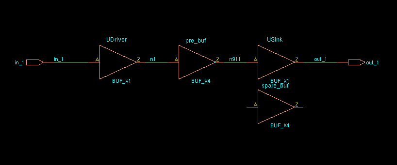
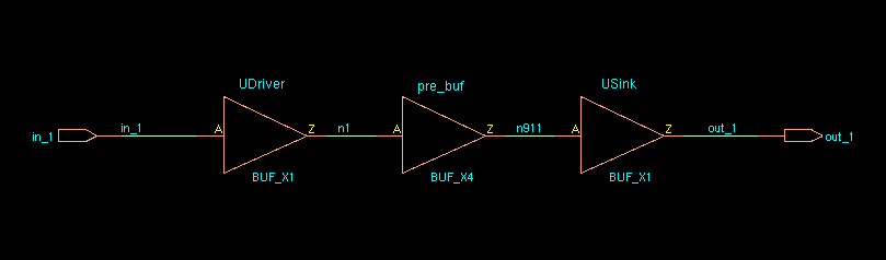
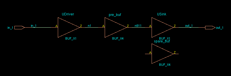
How
does EDI System identify spare cells in a post-mask ECO flow?
How
does EDI System identify spare cells in a post-mask ECO flow?
Spare cells should have a unique string in their instance name to
identify them. Then the command specifySpareGate or
ecoDesign -useSpareCells patternName is run to identify the
spare instances. For example, if all spare cells have _spare_ in their
name then they are identified using:
1
specifySpareGate -inst *_spare_*
OR
1
ecoDesign -spareCells *_spare_* ...
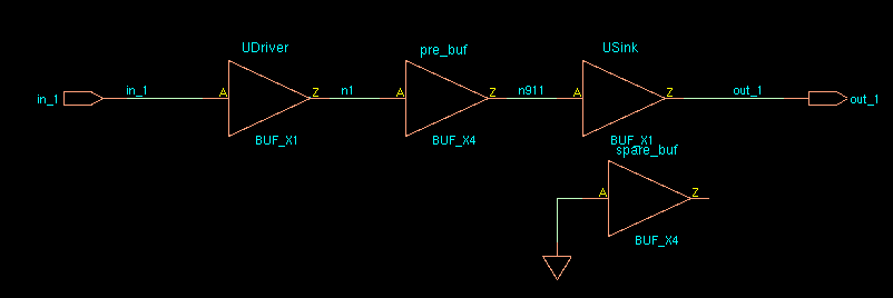
Note: if you are making manual ECO
changes to a netlist and converting a spare cell to a logical instance,
it's important to change the instance name. Otherwise,
the instance may be identified as a spare cell if a future ECO is
performed because it still has the spare cell instance name.
Note: sparecell's pointer and name is swapped with
the placed cell.
Error in "Innovus
Text Command Reference 21.12"
ecoSwapSpareCell
If the cell to be swapped is unplaced, it is mapped to the spare
cell. *instName* is deleted, and its connection is
transferred to the spare cell. If the cell to be swapped is placed, it
is swapped with the spare cell and is renamed to
*instNameSuffix* if the -suffix option is
used. If a suffix is not specified, the *instName* cell is
renamed to *spareCellInstName*. The *instName*
cell's connections are transferred to *spareCellInstName*.
The input of *instName* is tielo, based on the
global connection definition.