devops
OBS 无声录制带有声音的视频
录制视频时,想要 obs 能录制声音,但是不想人耳听到。
pactl load-module module-virtual-sink sink_name=VAC
unfortunately, Virtual audio sinks & settings gone after reboot
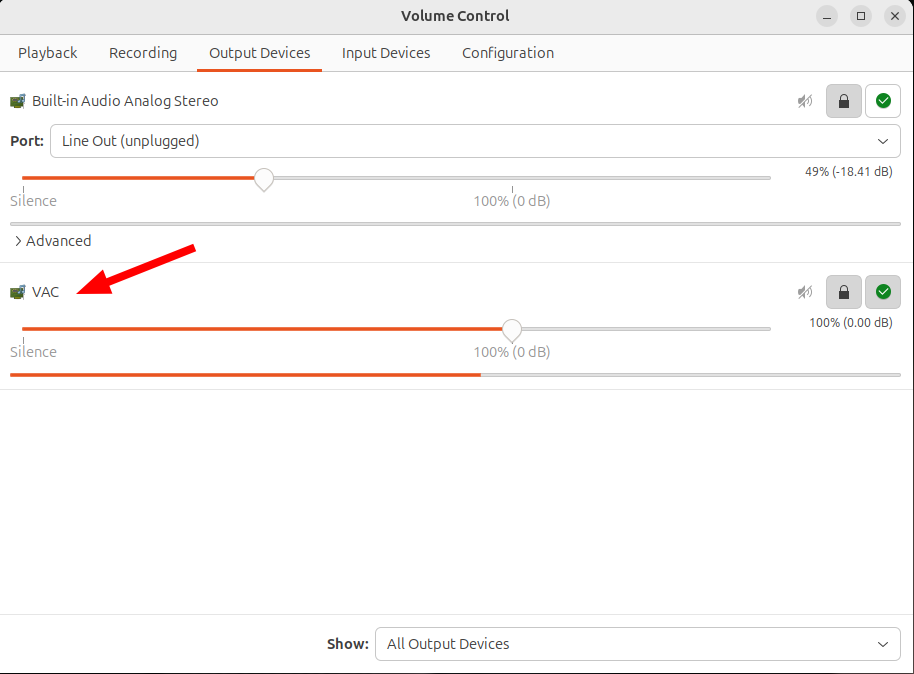
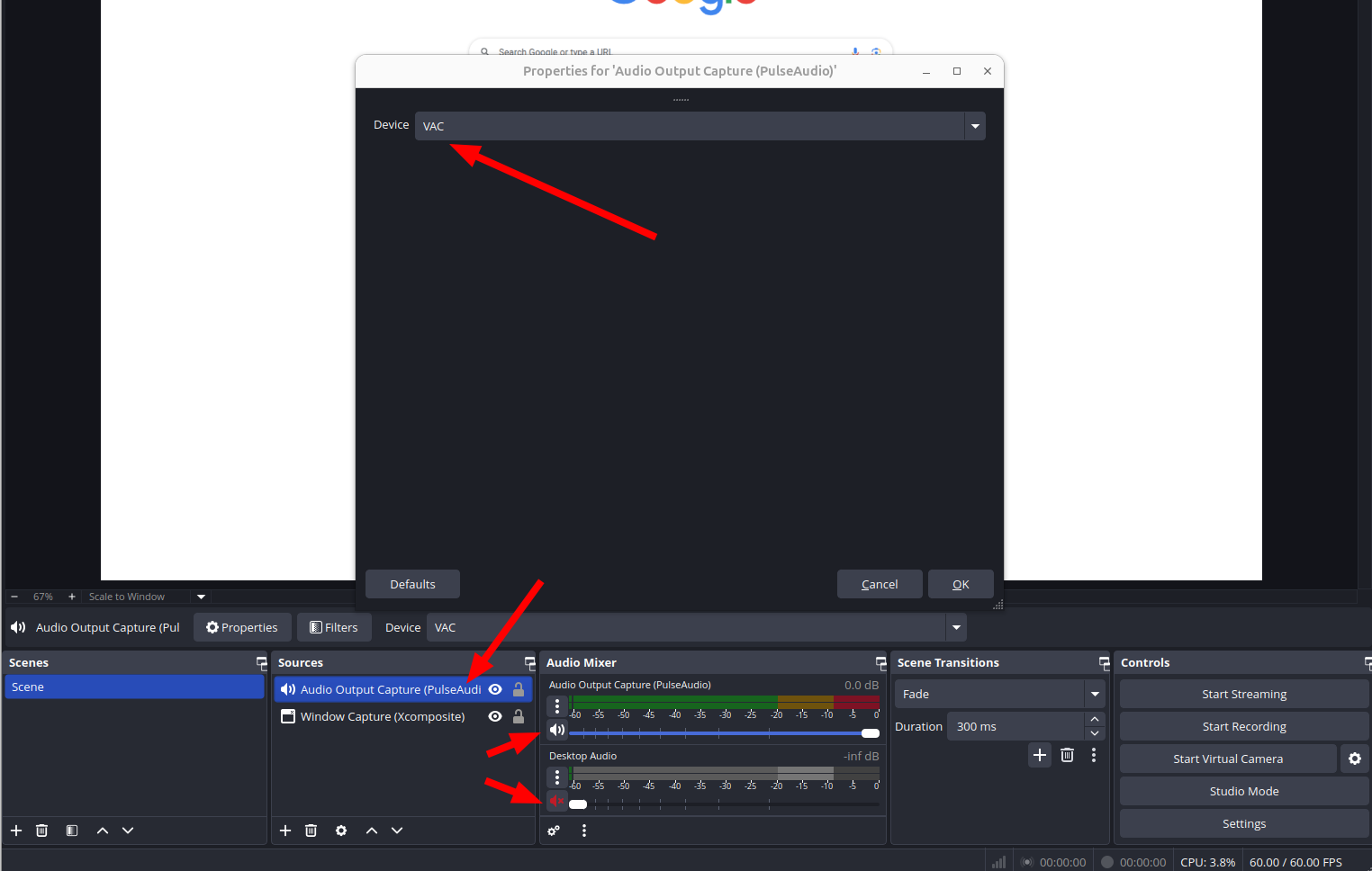
obs 无声录制带有声音的视频 [https://www.cnblogs.com/wztshine/p/17764073.html]
Virtual Audio Cable For Ubuntu [https://askubuntu.com/a/1268269/845522]
能不能设置个定时器,让录像自动停? [https://www.reddit.com/r/obs/comments/j5j1qa/comment/g7sk588/]
wget fetch a directory
1 | $ wget -r -np -R "index.html*" http://example.com/configs/.vim/ |
Using wget to recursively fetch a directory with arbitrary files in it [https://stackoverflow.com/a/273776/8037585]
mount/umount ISO
1 | $ sudo mount -t auto -o loop /path/to/matlab.iso /mnt/matlab |
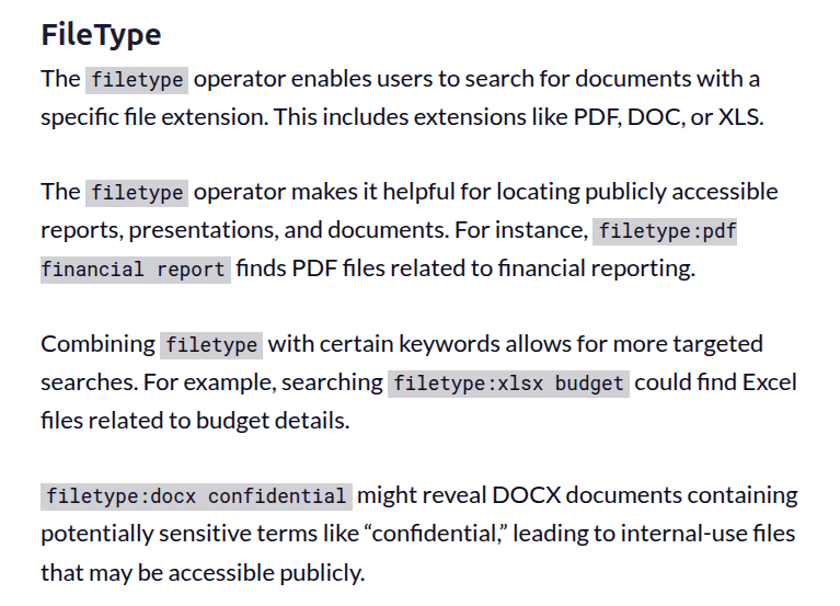
Google search tips

Restart Xfce panel
1 | xfce4-panel -r |
Rocky Linux 8 rpm for cadence binary and cdnshelp
qt5 and openssl
1 | sudo yum install openssl compat-openssl10 qca-qt5-ossl.x86_64 openssl-devel |
library preparation for EDA installation
1 | libc6, gdb |
Rocky Linux 8 extend LVM in VMware
1 | 1) gparted extend |
compile vim from source with GUI support
1 | # gtk3 in Rocky Linux 8.5 |
binkey
Inserting a new line below: o
above: O
To insert before the cursor: i
After: a
Before the line (home): I
Append at the end of line: A
network connection using nmcli
Problem
There is no network connection and device is not managed
1 | $ nmcli device status |
solution
1 | sudo nmcli networking on |
Then, eth0 is connected
1 | $ nmcli device status |
What is the proper method to remove old kernels from a Red Hat Enterprise Linux system?
Red Hat Enterprise Linux 8
The YUM version 4 (based on the upstream DNF project)
method for removing kernels and keeping only the latest version and
running kernel:
1 | $ yum remove --oldinstallonly |
From the yum man page:
1 | dnf [options] remove --oldinstallonly |
New windows and forms appear behind the Library Manager in background when using GNOME 3
Using Red Hat Enterprise Linux 8, Rocky Linux 8 and the GNOME 3 window manager, the new Virtuoso Schematic/Layout/ADE windows and forms sometimes pop up under or below the Library Manager or on the desktop in the background instead of the foreground and cannot be seen. Sometimes, they are iconized; they do not come on the top in front, though it is the most recent window opened.
solution
Install Focus my window GNOME Shell extension
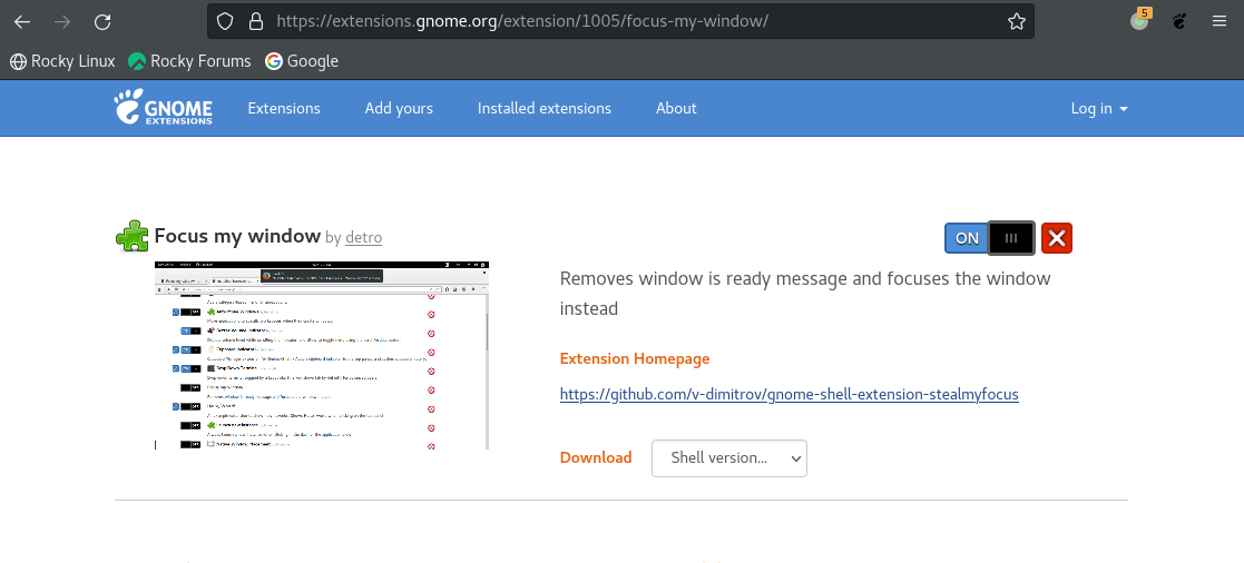
reference
Article (11612426) Title: New windows and forms appear behind the Library Manager in background or iconized instead of foreground on RHEL and SuSE Linux in GNOME, KDE Desktop, Metacity window manager URL: https://support.cadence.com/apex/ArticleAttachmentPortal?id=a1Od0000000nSXCEA2
VMware Disk Shrink
In Guest OS and run
1 | sudo vmware-toolbox-cmd disk shrink / |
https://superuser.com/q/211798
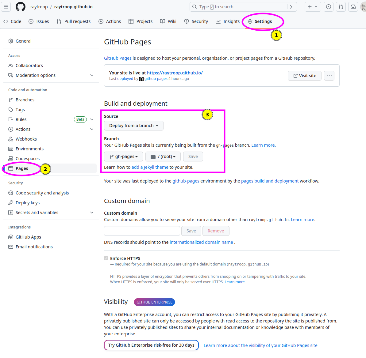
GitHub Pages Build and deployment
The repository visibility shall be public
How to squash all git commits into one?
https://stackoverflow.com/a/9254257/8037585
As of git
1.6.2, you can use git rebase --root -i
For each commit except the first, change pick to
squash.
this works find, but I had to do a forced push. be careful!
git push -f
Build VMware host modules
1 | git clone git@github.com:mkubecek/vmware-host-modules.git |
AWT-EventQueue-0 Matlab
1 | Renaming libstdc++.so.6 to libstdc++.so.6old solved it for me in MATLAB 2021B UBUNTU 20.04. Thanks! |
[https://www.mathworks.com/matlabcentral/answers/329796-issue-with-libstdc-so-6#comment_2316900]