Logic Gate & Synthesis
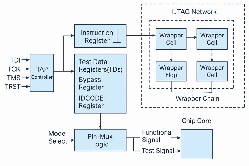
IJTAG
While JTAG connects chips externally, IJTAG extends it inside the chip — linking embedded instruments (MBIST, sensors, monitors, etc.) through a reconfigurable network.
Pin-Mux Logic Pins are precious in SoC design!
- Pin-Mux Logic lets functional and test signals share the same pins depending on the mode.
- During test mode, JTAG/IJTAG signals are routed internally via multiplexers — saving pins and silicon area.
Digital Delay Model
Akio Kitagawa, Analog layout design https://mixsignal.files.wordpress.com/2013/03/analog-layout.pdf
THE WIRE http://bwrcs.eecs.berkeley.edu/Classes/icdesign/ee141_f01/Notes/chapter4.pdf
Anoop Veliyath, Design Engineer, Cadence Design Systems. Accurately Modeling Transmission Line Behavior with an LC Network-based Approach [pdf]
Mark Horowitz. Lecture 2: Wires and Wire Models [pdf]
Neil Weste and David Harris. 2010. CMOS VLSI Design: A Circuits and Systems Perspective (4th. ed.). Addison-Wesley Publishing Company, USA.
Cheng-Kok Koh. EE695K Modeling and Optimization of High Performance Interconnect [lec3a_pdf]
Vishal Saxena. ECE 445 Intro to VLSI Design: Lectures for Spring 2019 https://www.eecis.udel.edu/~vsaxena/courses/ece445/s19/ECE445.htm
Effective Switching resistance
https://www.eecis.udel.edu/~vsaxena/courses/ece445/s19/Lecture%20Notes/lec15_ece445.pdf
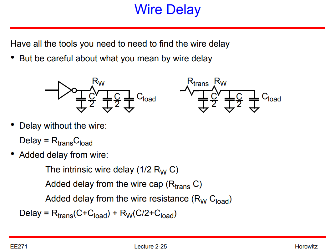
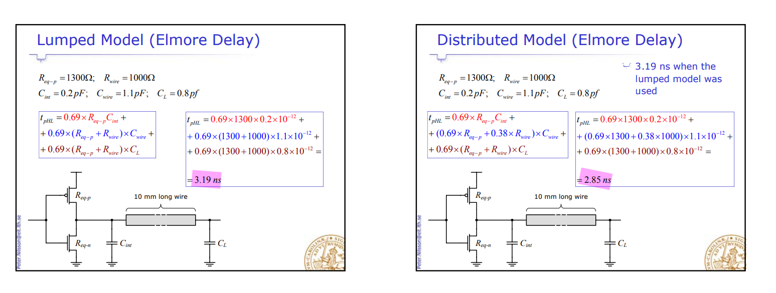
wire delay
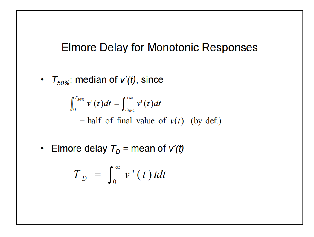
Elmore Delay
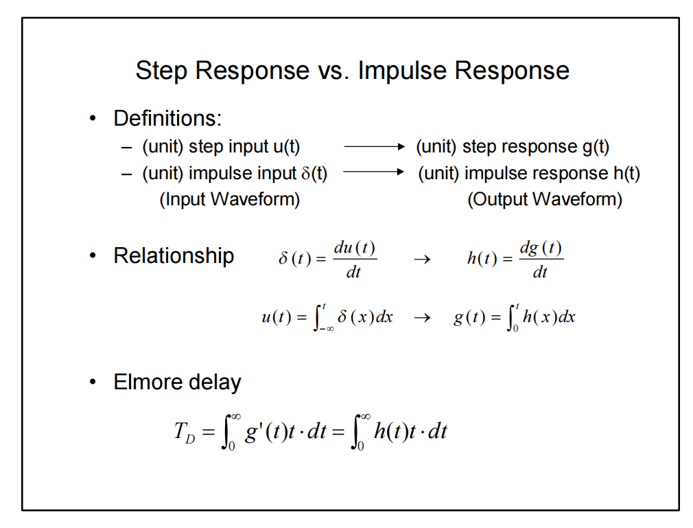
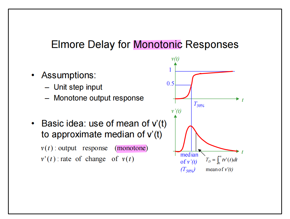
Basic idea: use of mean of \(v'(t)\) to approximate median of \(v'(t)\)
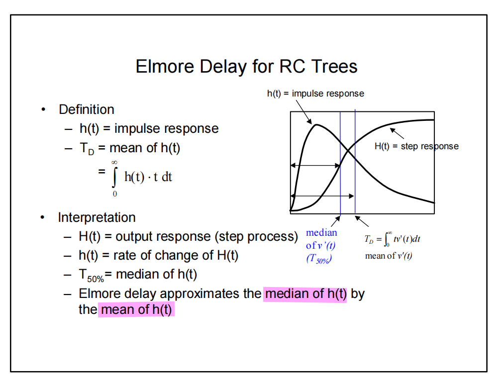
Elmore delay approximates the median of \(h(t)\) by the mean of \(h(t)\)
Distributed RC-Line
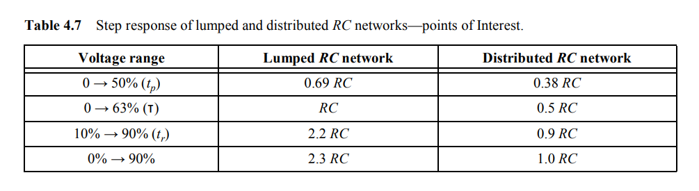
Lumped approximations
\(rc\)-models
If your simulator does not support a distributed \(rc\)-model, or if the computational complexity of these models slows down your simulation too much, you can construct a simple yet accurate model yourself by approximating the distributed \(rc\) by a lumped RC network with a limited number of elements
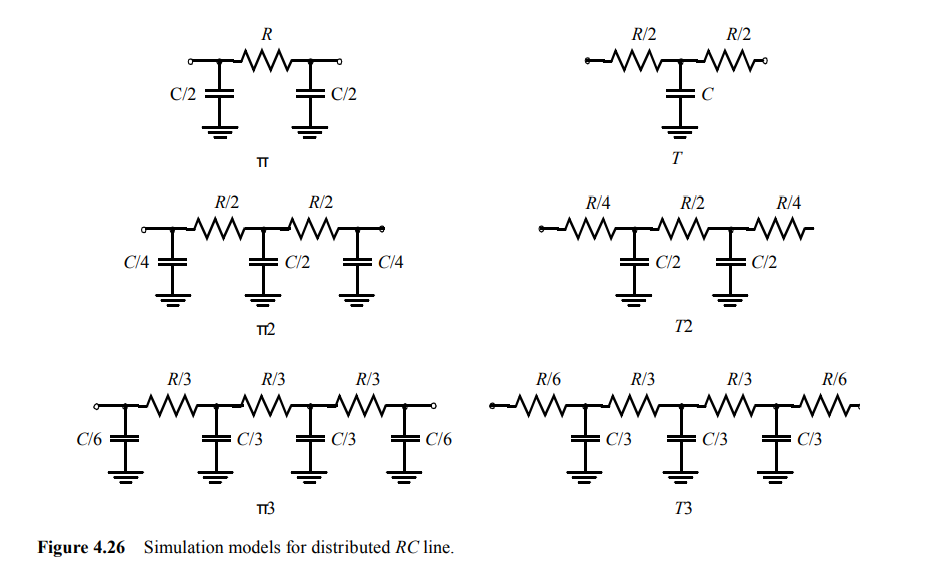
The accuracy of the model is determined by the number of stages. For instance, the error of the \(\Pi -3\) model is less than 3%, which is generally sufficient.
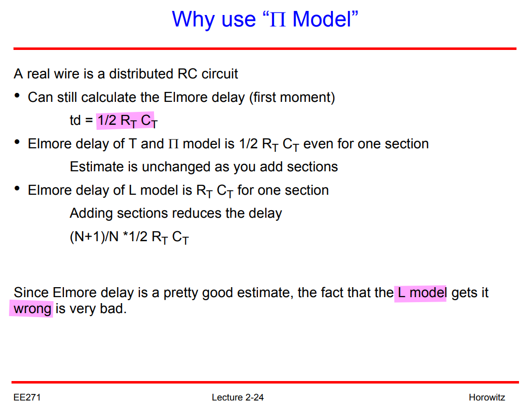
Why use "\(\Pi\) Model"
examples
Wire Inductive Effect
- RC delay increases quadratically with length
- LC delay (speed of light flight time) increases linearly with length
Inductance will only be important to the delay of low-resistance signals such as wide clock lines
wave
Signal propagates over the wire as a wave (rather than diffusing as in \(rc\) only models)
Signal propagates by alternately transferring energy from capacitive to inductive modes
Glitches & Hazards
CPE166/EEE 270 Advanced Logic Design-Digital Design: Time Behavior of Combinational Networks: https://www.csus.edu/indiv/p/pangj/166/f/sram/Handout_Hazard.pdf
John Knight, ELEC3500 Glitches and Hazards in Digital Circuits http://www.doe.carleton.ca/~shams/ELEC3500/hazards.pdf
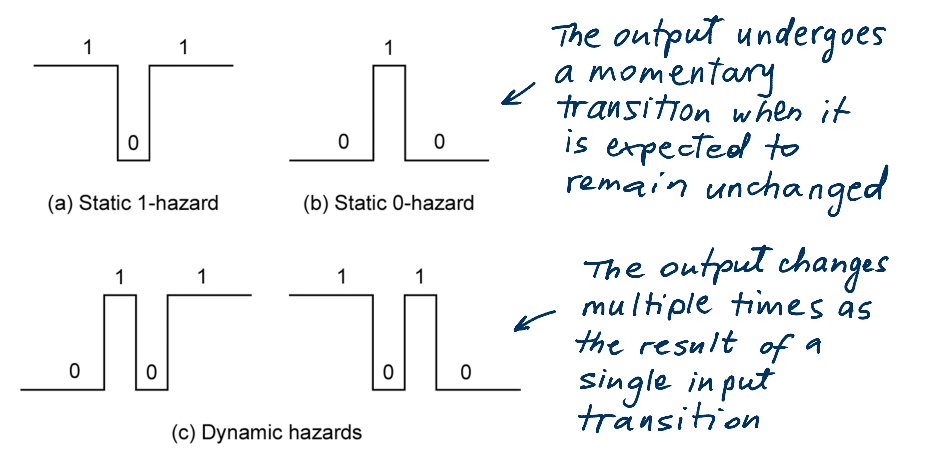
- A glitch is an unwanted pulse at the output of a combinational logic network – a momentary change in an output that should not have changed
- A circuit with the potential for a glitch is said to have a hazard
- In other words a hazard is something intrinsic about a circuit; a circuit with hazard may or may not have a glitch depending on input patterns and the electric characteristics of the circuit.
When do circuits have hazards ?
Hazards are potential unwanted transients that occur in the output when different paths from input to output have different propagation delays
Types of Hazards (on an output)
static 1-hazard, static 0-hazard, dynamic hazard
Hazard's Concern
- Hazards do not hurt synchronous circuits
- Hazards Kill Asynchronous Circuits
- Glitches Increase Power Consumption
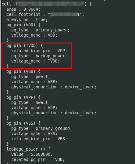
Isolation cells
Isolation cells and Level Shifter cells URL: https://vlsitutorials.com/isolation-cells-level-shifter-cells-low-power-vlsi/
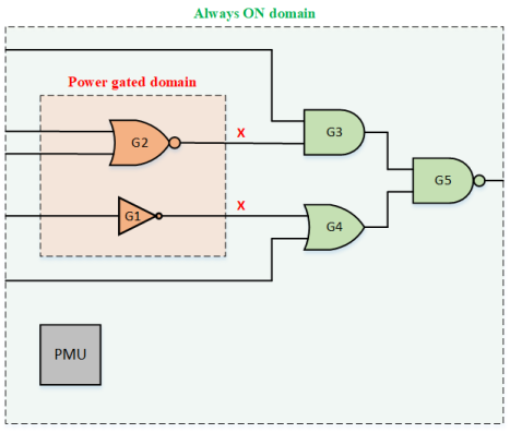
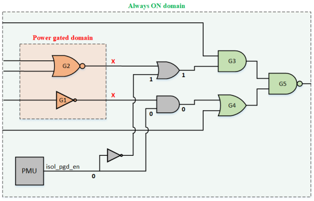
Isolation cells are additional cells inserted by the synthesis tools for isolating the buses/wires crossing from power-gated domain of a circuit to its always-on domain (AON).
To prevent corruption of always-on domain, we clamp the nets crossing the power domains to a value depending upon the design.
A simple circuit having a switchable (or gated) power domain
The circuit shown in Figure 1, after isolation cells are inserted
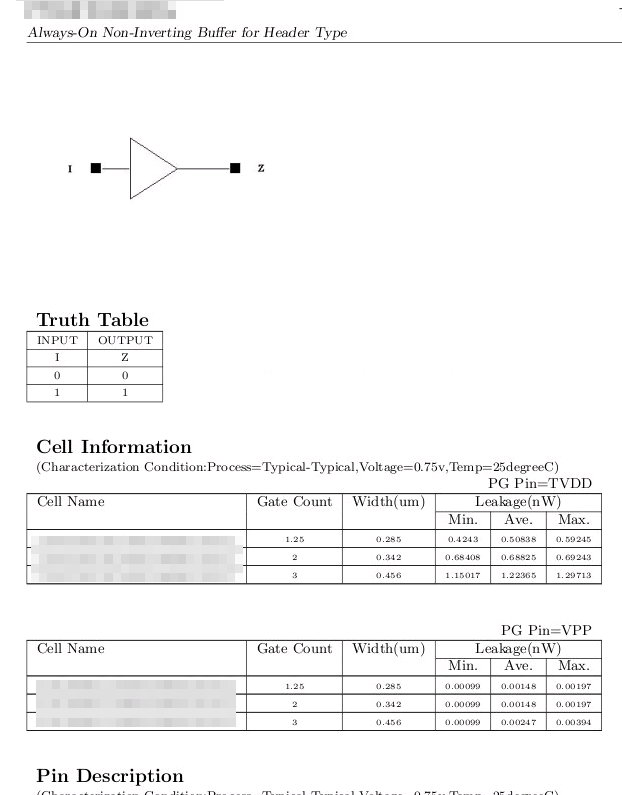
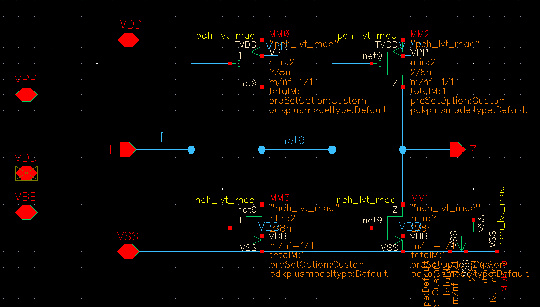
Always-On Buffer
Clock Gating
The Ultimate Guide to Clock Gating https://anysilicon.com/the-ultimate-guide-to-clock-gating/
Clock Gating is defined as: "Clock gating is a technique/methodology to turn off the clock to certain parts of the digital design when not needed".
AND gate-based clock gating
In simplest form a clock gating can be achieved by using an AND gate as shown in picture below
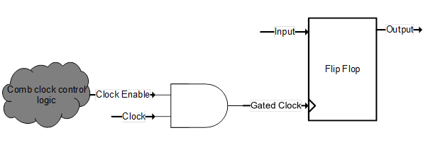
However, this simplest form of clock gating technique has some problem of generating glitches in the clock provide to the FF, which are not desirable.
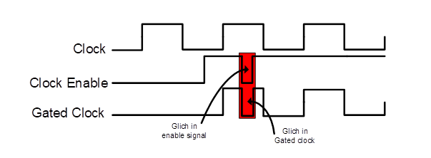
Glitches in enable/gated clock
Latch based clock gating
These glitches can be removed by introducing a negative edge triggered FF (assuming downstream FFs are positive edge) or low-level sensitive latch at the output of the clock enable signal.
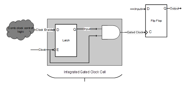
This will make sure that any glitch in the clock enable signal will not be visible to the gated clock output. The Latch output will only be updated during the negative clock cycle and thus input to AND gate will be stable high.
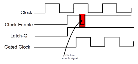
Glitch Free Gated Clock
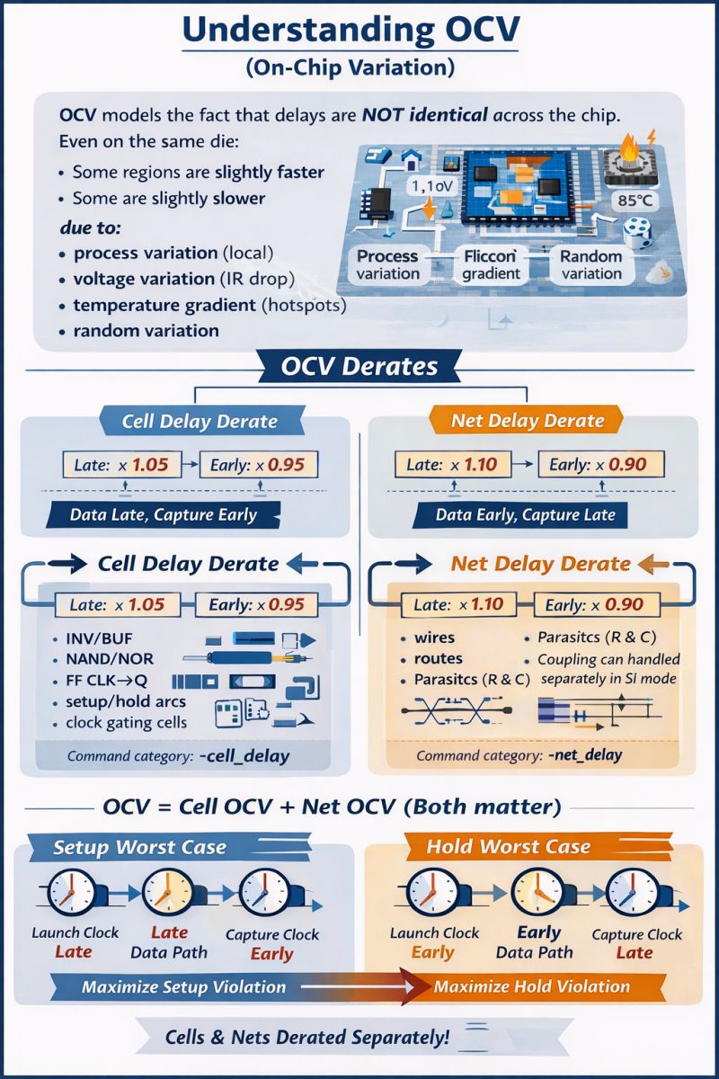
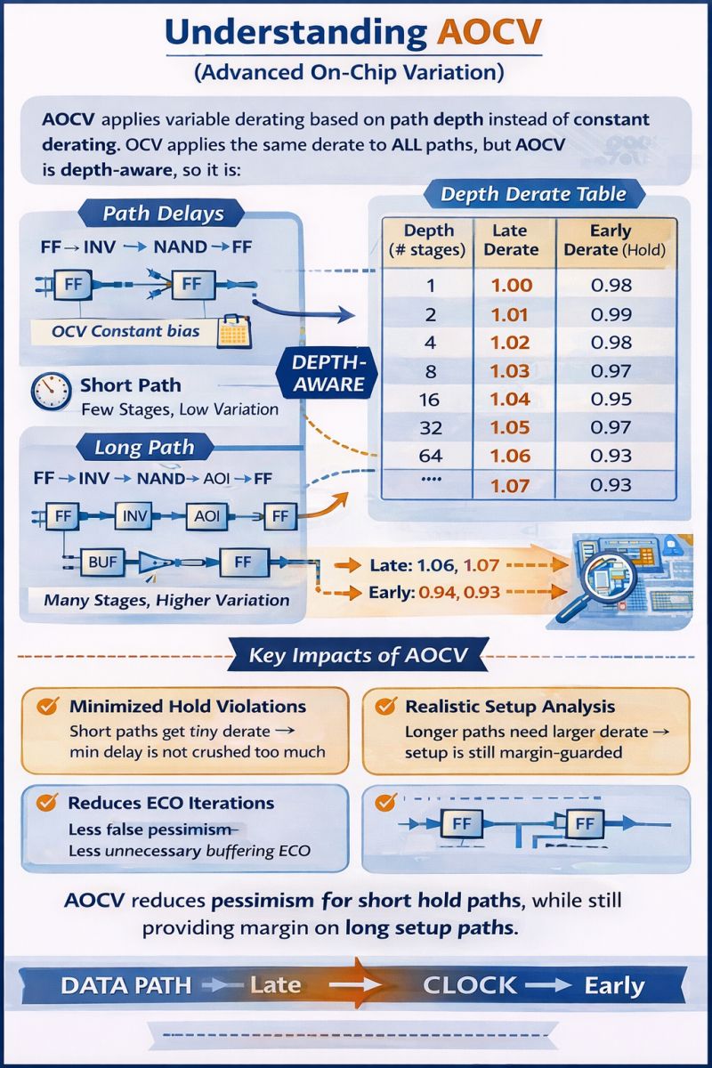
OCV Derating With AOCV
Genus Attribute Reference 22.1
Innovus Text Command Reference 22.10
Article (20416394) Title: Analysis with Advanced On-chip Variation (AOCV) derating in EDI system and ETS
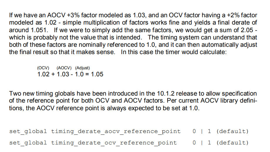
timing_aocv_derate_mode
1 | timing_aocv_derate_mode{aocv_multiplicative | aocv_additive} |
Default: aocv_multiplicative
Controls the AOCV derating mode.
When set to aocv_multiplicative, the derating factor
will be calculated as AOCV derating * OCV derating, which is set using
the set_timing_derate command.
When set to aocv_additive, the derating factor will be
calculated as AOCV derating + OCV derating values.
When you use this global variable, the report_timing
command shows the total_derate column in the timing report
output, which allows you to view and cross-check the calculated total
derate factor.
To set this global variable, use the set_global
command.
Sulege Vivek [link]
preserve hand-instantiated cells
To preserve the hand-instantiated cells
1 | set_dont_touch [get_cells -hierarchical *dont_touch_*] |
The instances whose name contain "dont_touch_" shall be preserved during synthesis
1 | // no performace concerns, rest sync use sync3 is enough |