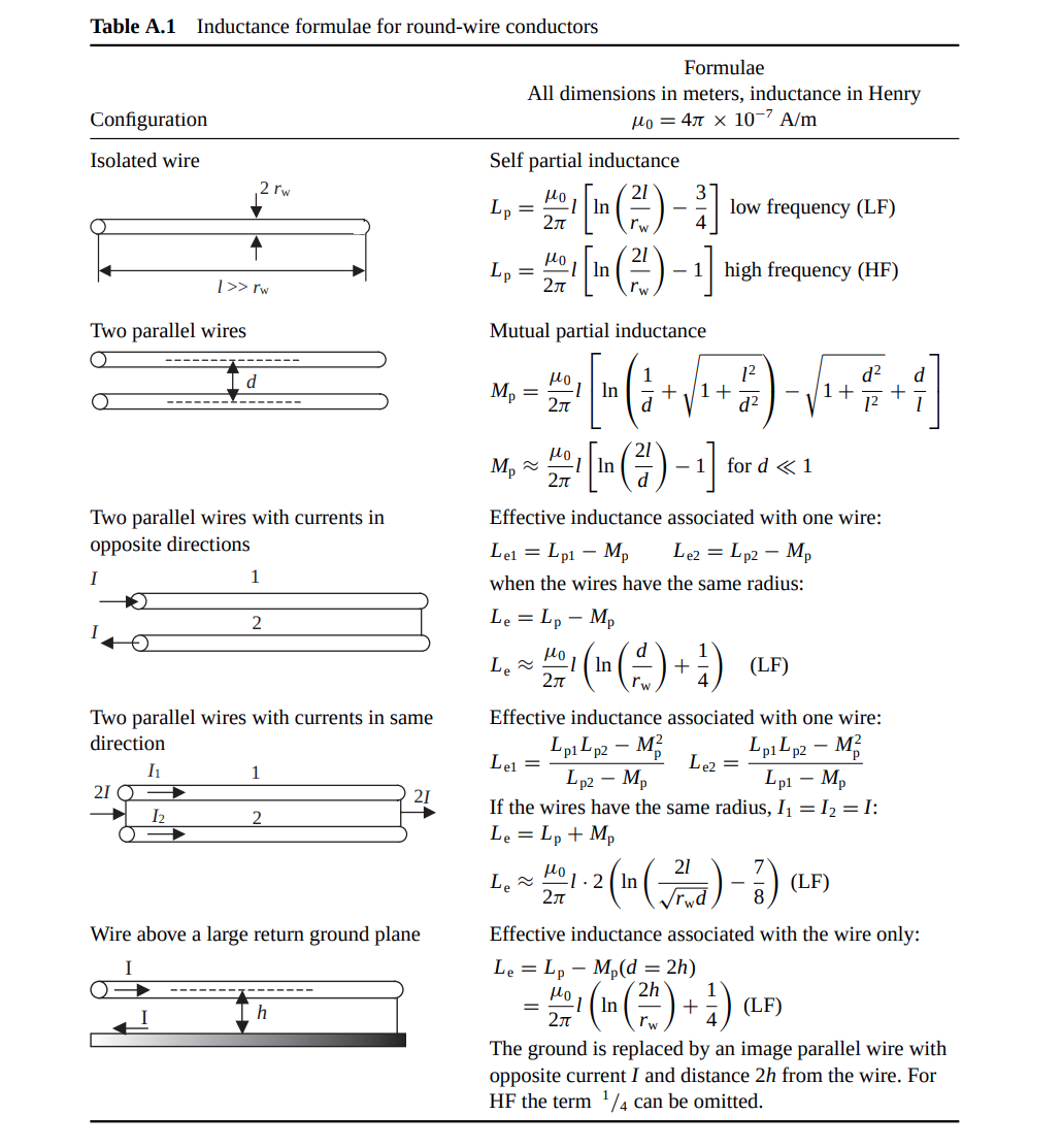
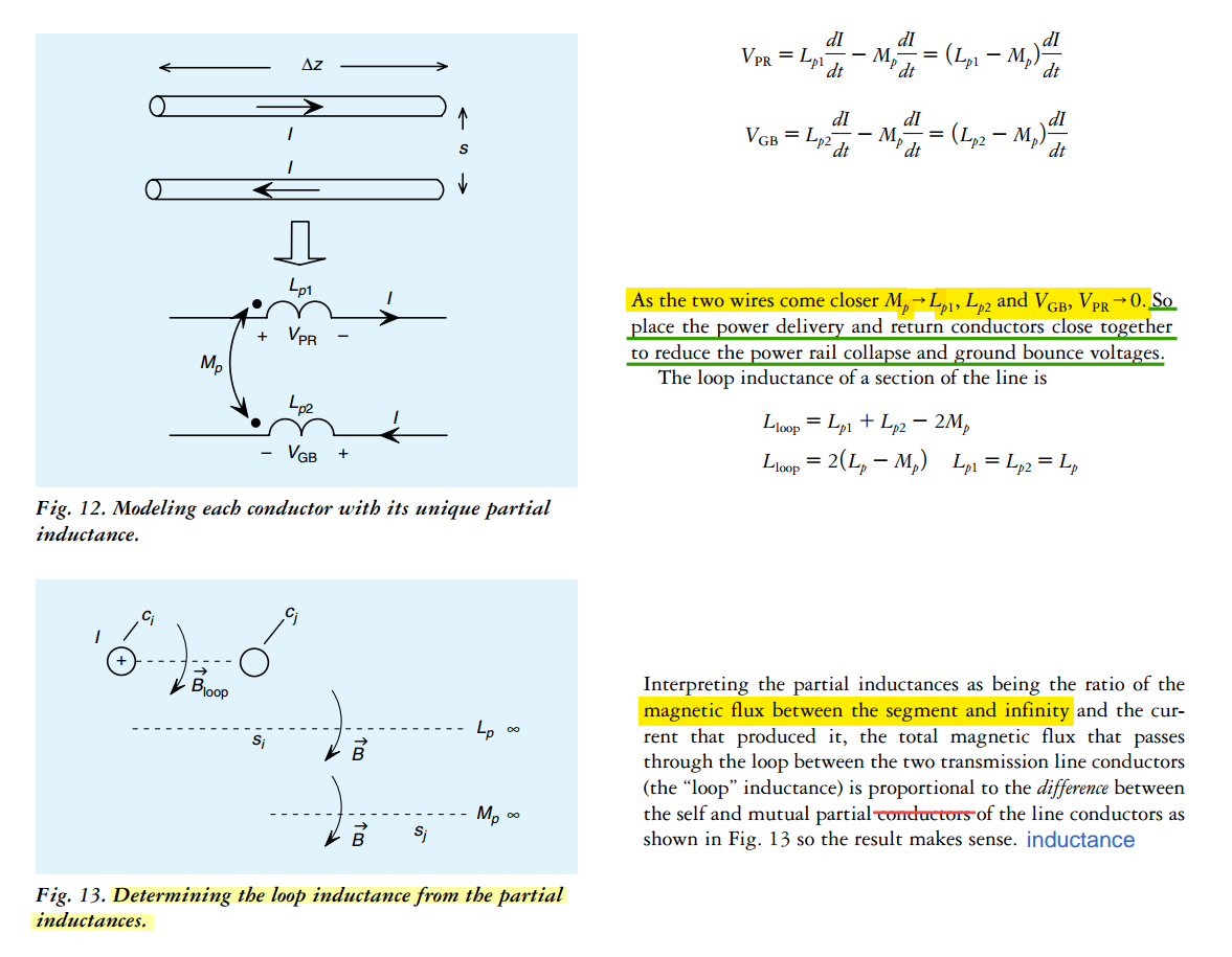
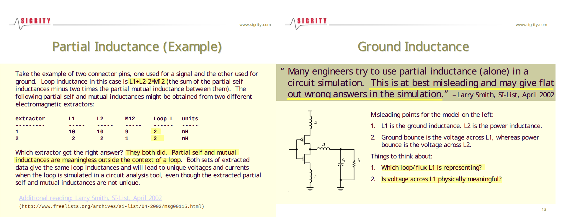
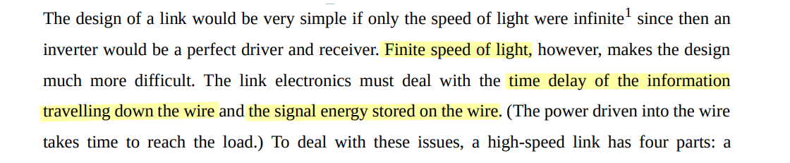
Partial Inductance
Loop Inductance is the sum of partial self-inductance and partial-mutual inductance
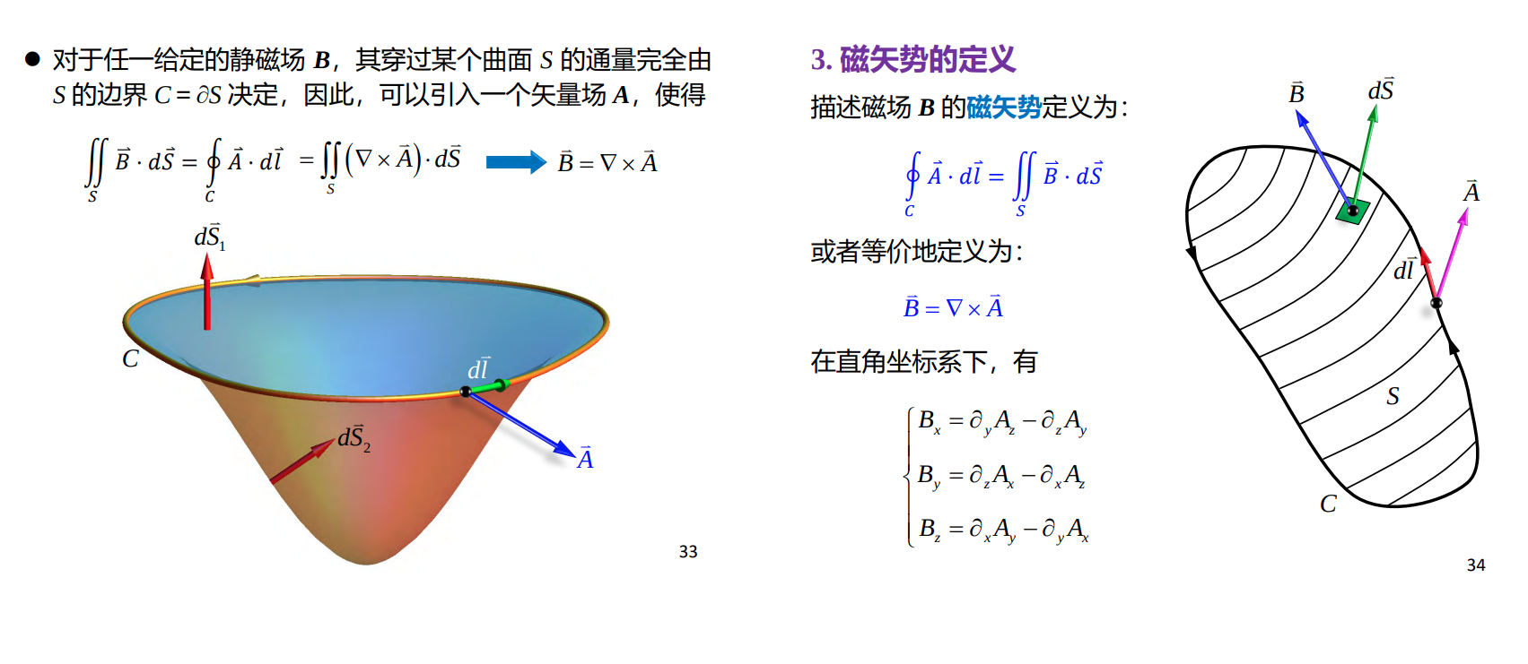
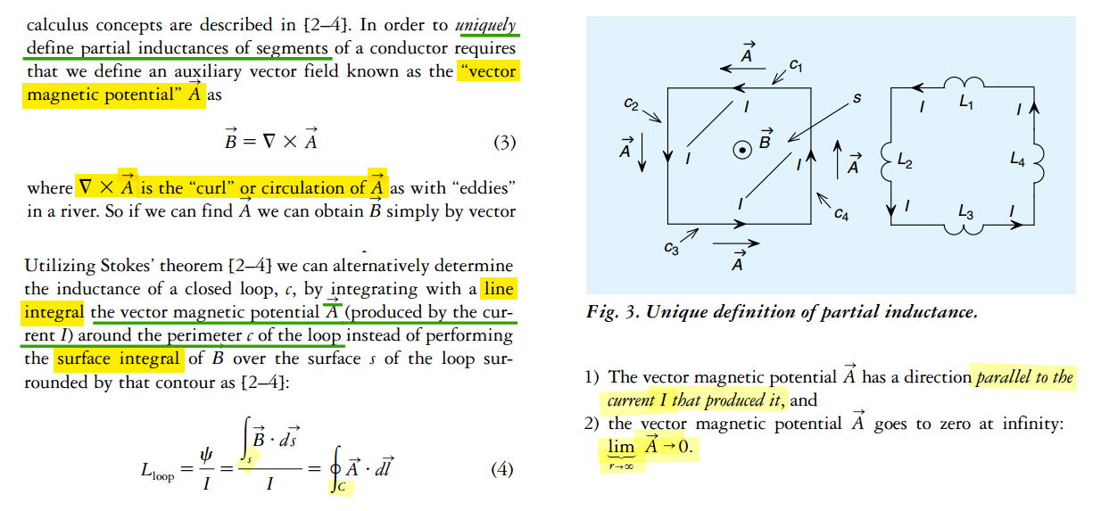
Magnetic Vector Potential (磁矢势)
Youjin Deng. 5-3 静磁场的基本规律 [http://staff.ustc.edu.cn/~yjdeng/EM2022/pdf/5-2(2022).pdf]
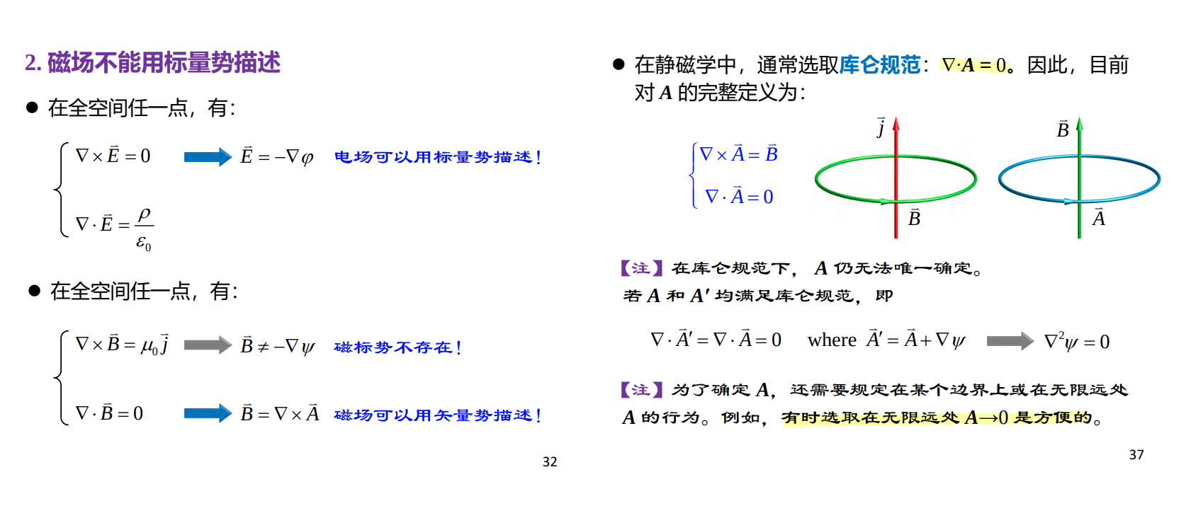
磁场不能用标量势描述
Partial Inductance
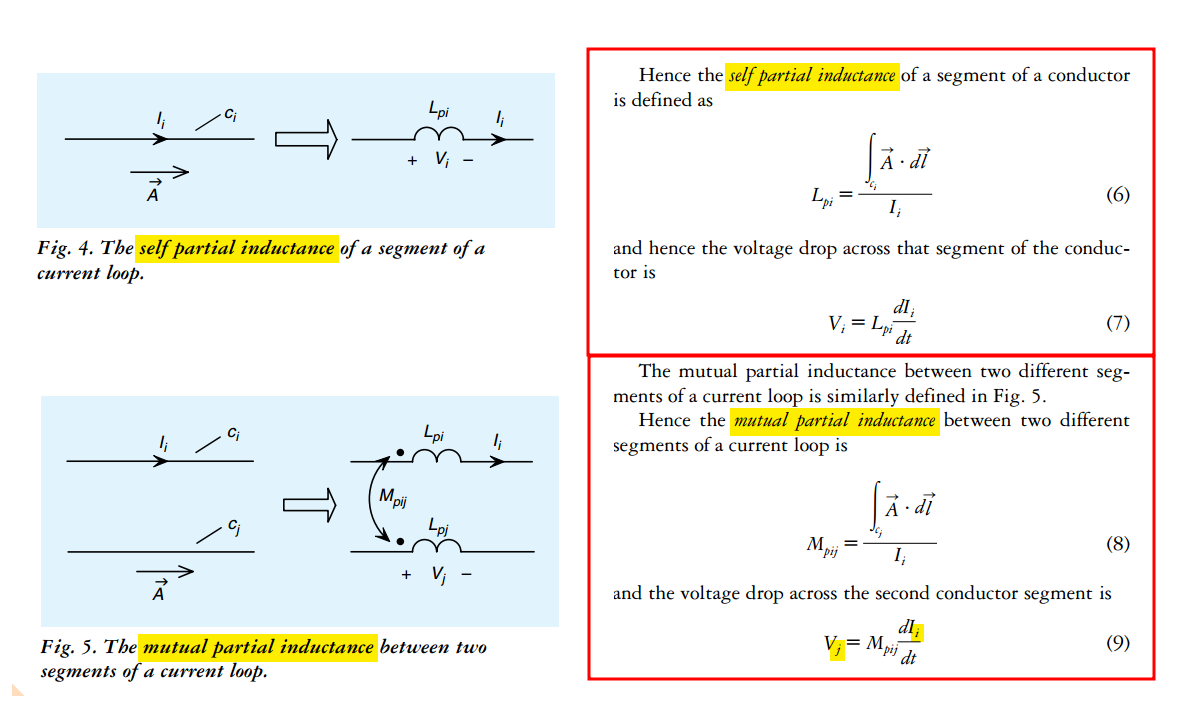
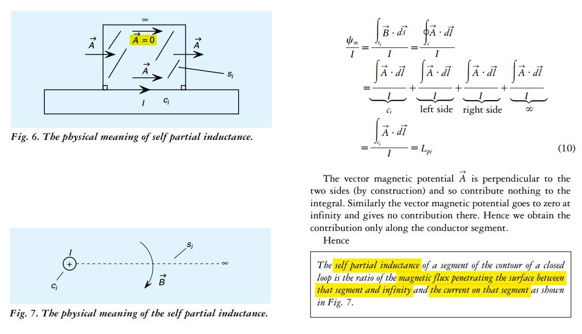
self partial inductance
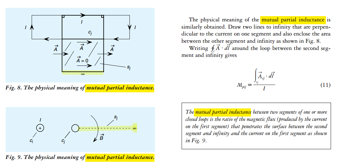
mutual partial inductance
Ex. two-wire
[https://www.oldfriend.url.tw/Q3D/ansys_ch_Partial_Loop_Inductance.html]
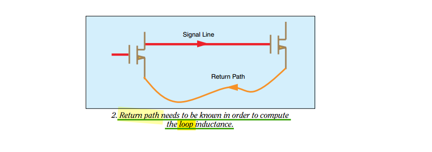
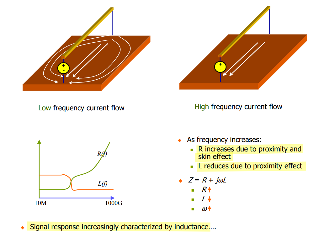
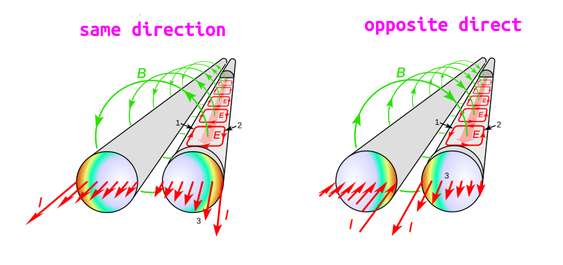
Current Return Path
Current return paths are frequency dependent \(Z = R +j\omega L\)
- Low frequency
- \(R\) dominates - current use as many returns as possible to have parallel resistances
- High frequency
- \(j\omega L\) dominates - current use the closest possible return path to form the smallest possible loop inductance
- Very high frequency
- The current would be confined to the nearest possible return only at ultra-high frequencies (skin effect)
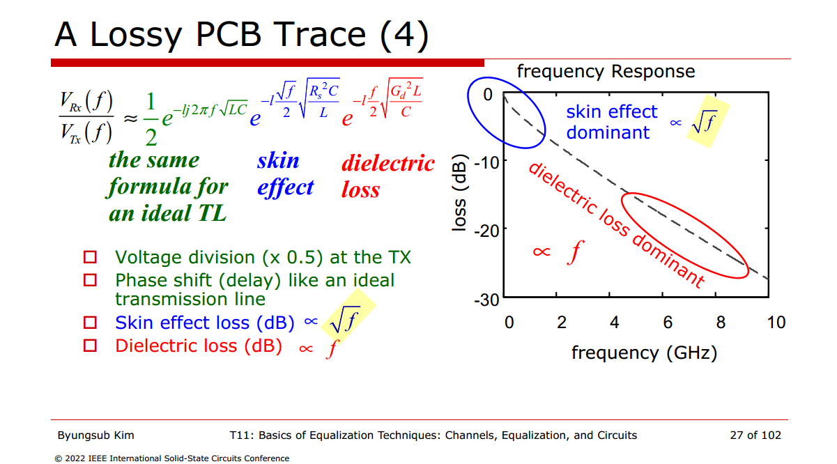
skin effect & Dielectric loss
EMX simulation
setup:
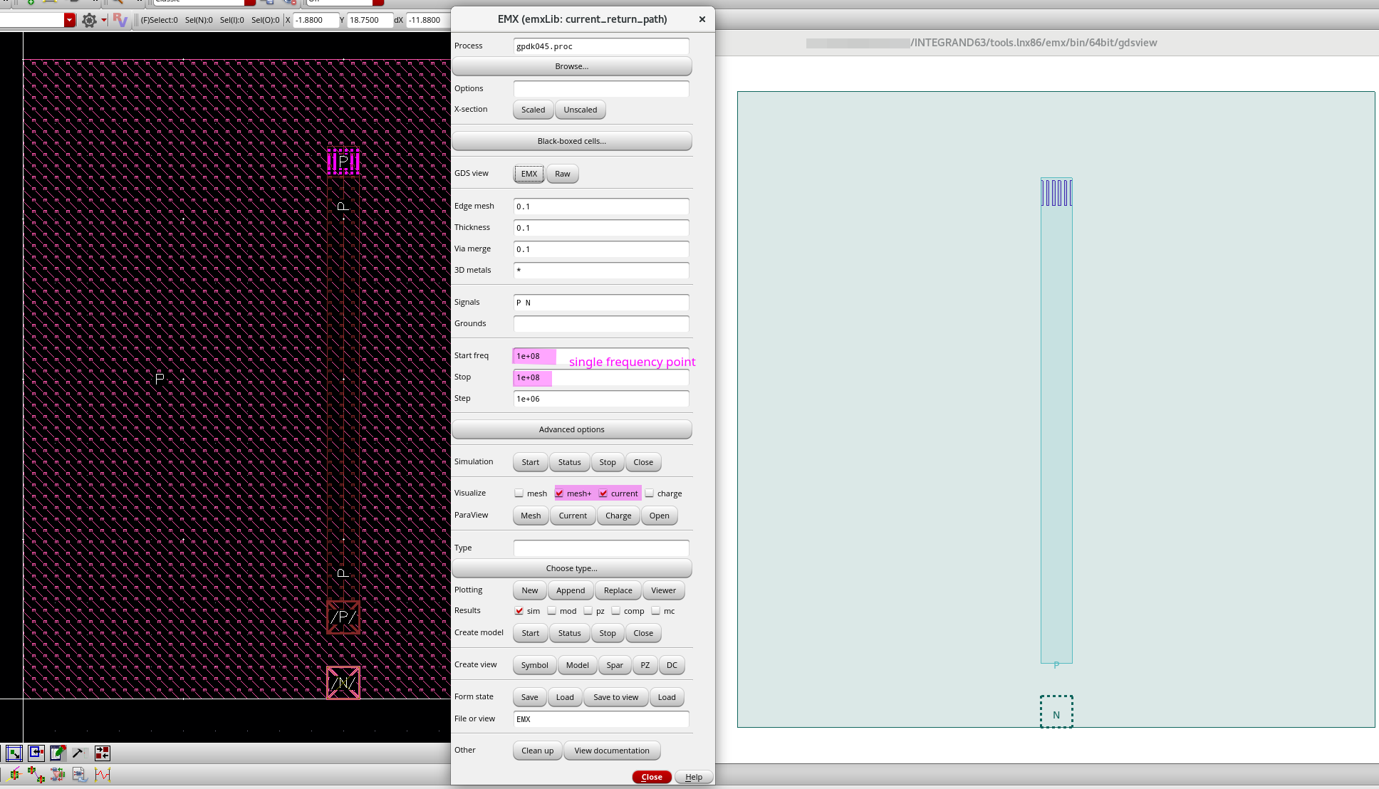
frequency sweep:
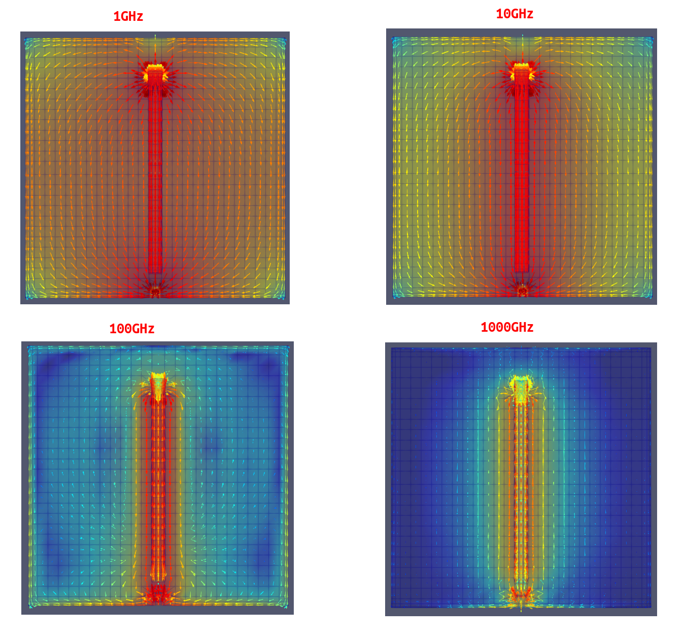
Cadence October 2020, Analysis of a Figure-Eight Inductor with EMX RAK
proximity effect & skin effect
- Skin effect concentrates current near the surface of a single conductor, while proximity effect concentrates current in specific regions of multiple conductors due to their interaction
- Skin effect is caused by the conductor's own magnetic field, while proximity effect is caused by the magnetic field of a nearby conductor
proximity effect is a redistribution of electric current occurring in nearby parallel electrical conductors carrying alternating current (AC), caused by magnetic effects (eddy currents)
skin effect is the tendency of AC current flow near the surface (or "skin") of a conductor, rather than throughout its cross-section, due to the magnetic field generated by the current itself
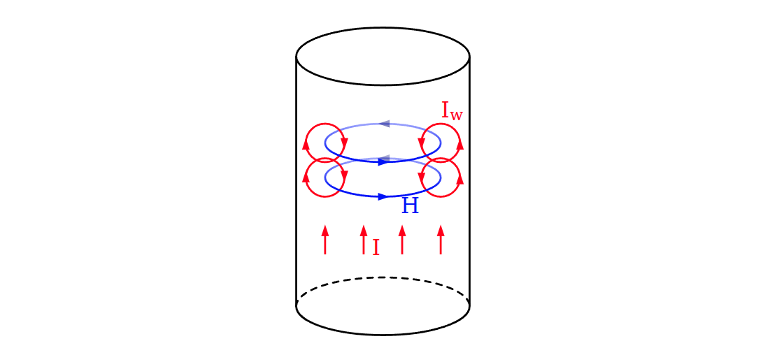
Cause of skin effect
A main current \(I\) flowing through a conductor induces a magnetic field \(H\). If the current increases, as in this figure, the resulting increase in \(H\) induces separate, circulating eddy currents \(I_W\) which partially cancel the current flow in the center and reinforce it near the skin
Eddy current
By Lenz's law, an eddy current creates a magnetic field that opposes the change in the magnetic field that created it, and thus eddy currents react back on the source of the magnetic field
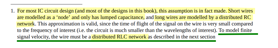
RLC network
[https://web.stanford.edu/class/archive/ee/ee371/ee371.1066/handouts/markChapt.pdf]
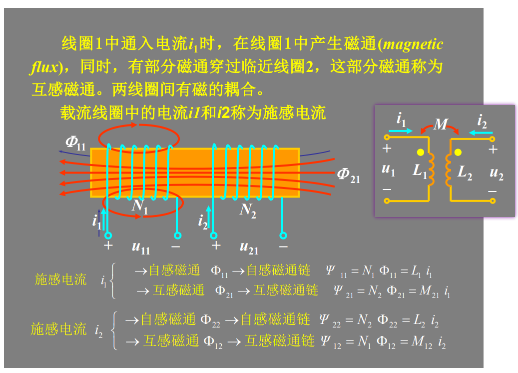
Transformer
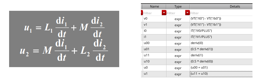
任何封闭电路中感应电动势大小,等于穿过这一电路磁通量的变化率。 \[ \epsilon = -\frac{d\Phi_B}{dt} \] 其中 \(\epsilon\)是电动势,单位为伏特
\(\Phi_B\)是通过电路的磁通量,单位为韦伯
电动势的方向(公式中的负号)由楞次定律决定
楞次定律: 由于磁通量的改变而产生的感应电流,其方向为抗拒磁通量改变的方向。
在回路中产生感应电动势的原因是由于通过回路平面的磁通量的变化,而不是磁通量本身,即使通过回路的磁通量很大,但只要它不随时间变化,回路中依然不会产生感应电动势。
自感电动势
当电流\(I\)随时间变化时,在线圈中产生的自感电动势为 \[ \epsilon = -L\frac{dI}{dt} \]
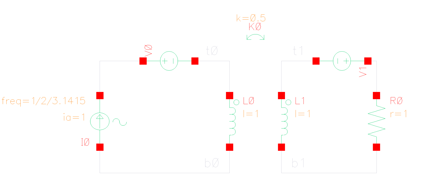
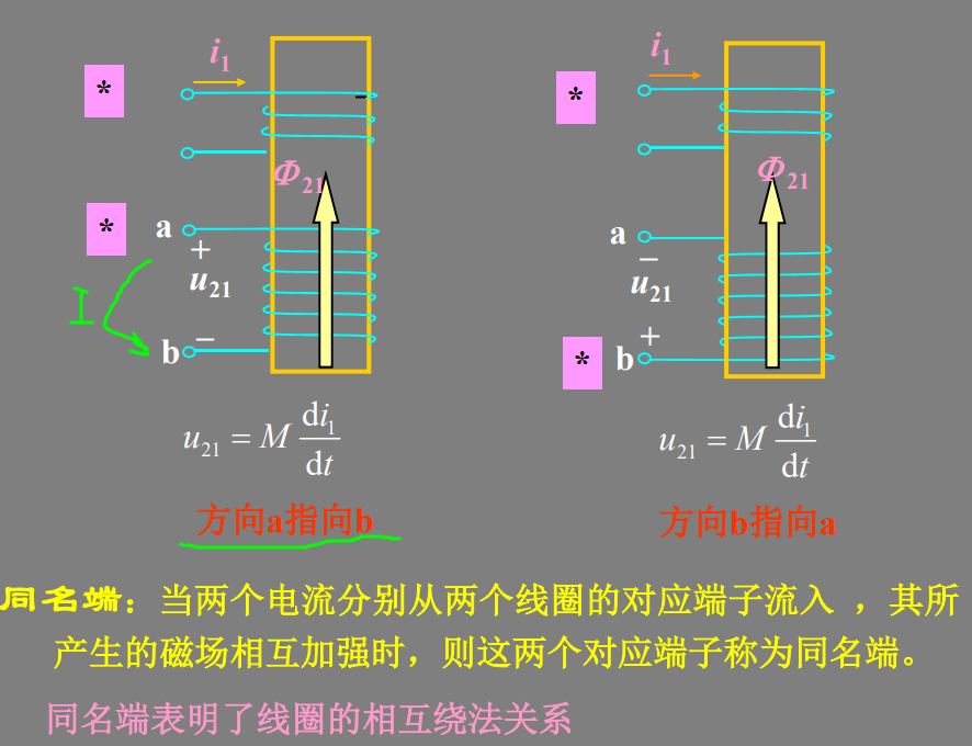
同名端:当两个电流分别从两个线圈的对应端子流入 ,其所 产生的磁场相互加强时,则这两个对应端子称为同名端。
reference
ISSCC2002. Special Topic Evening Discussion Sessions SE1: Inductance: Implications and Solutions for High-Speed Digital Circuits [vSE1_Blaauw], [vSE1_Gauthier], [vSE1_Morton, [vSE1_Restle]]
Y. Massoud and Y. Ismail, "Gasping the impact of on-chip inductance," in IEEE Circuits and Devices Magazine, vol. 17, no. 4, pp. 14-21, July 2001 [https://sci-hub.se/10.1109/101.950046]
Clayton R. Paul, Partial Inductance [https://ewh.ieee.org/soc/emcs/acstrial/newsletters/summer10/PP_PartialInductance.pdf]
Cheung-Wei Lam. Common Misconceptions about Inductance & Current Return Path [https://ewh.ieee.org/r6/scv/emc/archive/022010Lam.pdf]
Randy Wolff. Signal Loop Inductance in [Pin] and [Package Model] [https://ibis.org/summits/feb10/wolff.pdf]
ANSYS Q3D Getting Started LE05. Module 5: Q3D Inductance Matrix Reduction [https://innovationspace.ansys.com/courses/wp-content/uploads/sites/5/2021/07/Q3D_GS_2020R1_EN_LE05_Ind_Matrix.pdf]
Paul, Clayton R. Inductance: Loop and Partial. Hoboken, N.J. : [Piscataway, N.J.]: Wiley ; IEEE, 2010.
Spartaco Caniggia. Signal Integrity and Radiated Emission of High‐Speed Digital Systems. Wiley 2008
Yuriy Shlepnev. How Interconnects Work: Characteristic Impedance and Reflections [https://www.linkedin.com/pulse/how-interconnects-work-characteristic-impedance-yuriy-shlepnev/]
-. How Interconnects Work: Bandwidth for Modeling and Measurements [https://www.linkedin.com/pulse/how-interconnects-work-bandwidth-modeling-yuriy-shlepnev/?trackingId=874kpm3XuNyV9D0eP6IioA%3D%3D]
Eric Bogatin. Pop Quiz: When is an Interconnect Not a Transmission Line? [https://www.signalintegrityjournal.com/blogs/4-eric-bogatin-signal-integrity-journal-technical-editor/post/265-pop-quiz-when-is-an-interconnect-not-a-transmission-line]
TeledyneLeCroy/SignalIntegrity Python tools for signal integrity applications [SignalIntegrityApp]
A Look at Transmission-Line Losses [http://blog.teledynelecroy.com/2018/06/a-look-at-transmission-line-losses.html]
How Much Transmission-Line Loss is Too Much? [http://blog.teledynelecroy.com/2018/06/how-much-transmission-line-loss-is-too.html]
Raymond Y. Chen, Raymond Y. Chen. Fundamentals of S Fundamentals of S-Parameter Parameter Modeling for Power Distribution Modeling for Power Distribution System (PDS) and SSO Analysis System (PDS) and SSO Analysis [https://ibis.org/summits/jun05/chen.pdf]