Jitter
Voltage to Excess Phase Transformations
Excess phase as Random Noise
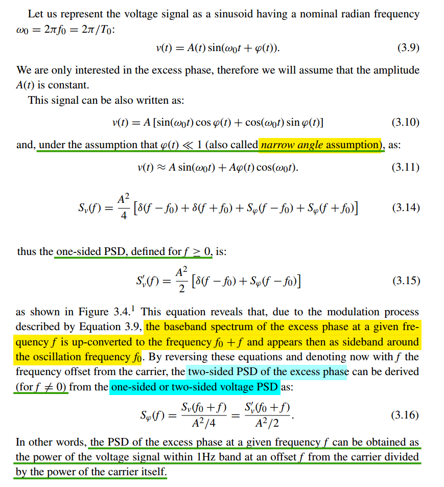
excess phase around \(n\)-th harmonic
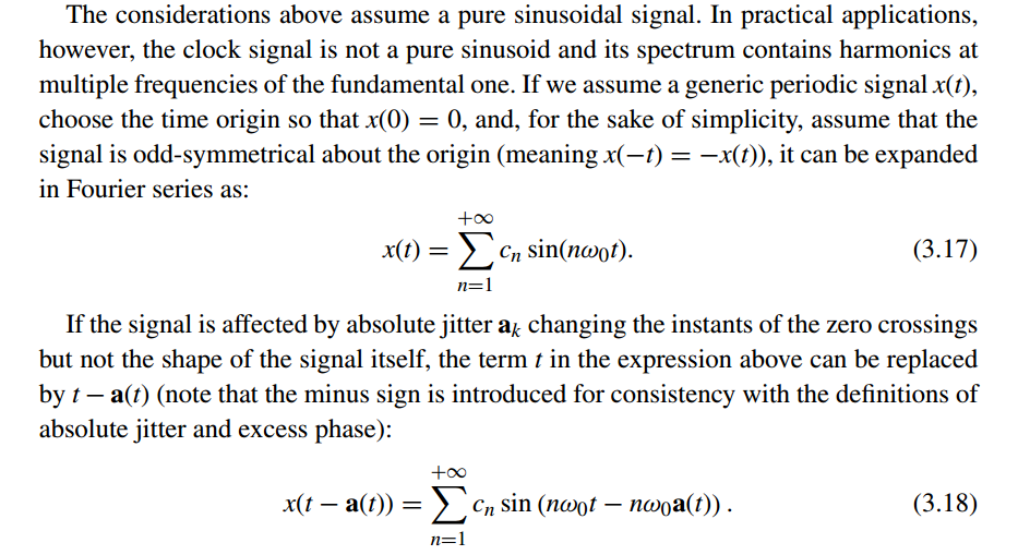
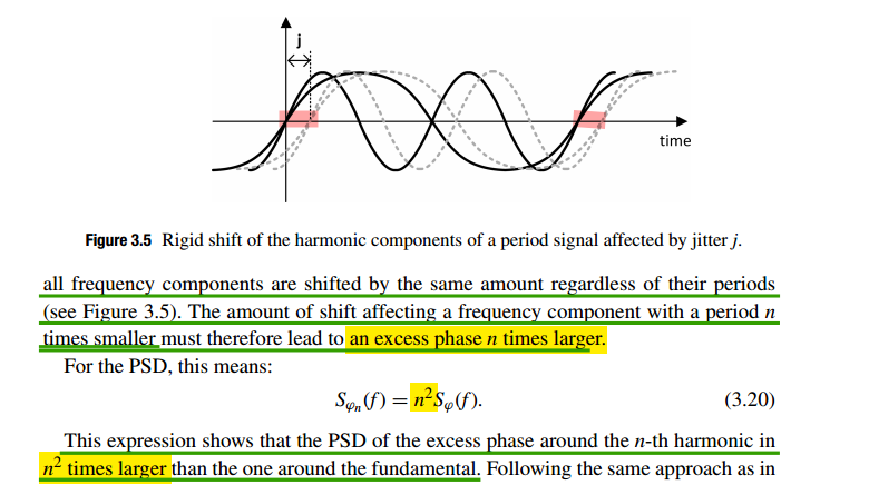
\(\Delta t\) is same for any n-th harmonic
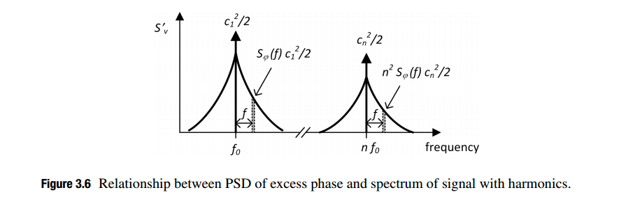
Excess phase as deterministic periodic signal
Nicola Da Dalt, ISSCC 2012: Jitter Basic and Advanced Concepts, Statistics and Applications
C. Samori, "Tutorial: Understanding Phase Noise in LC VCOs," 2016 IEEE International Solid-State Circuits Conference (ISSCC), San Francisco, CA, USA, 2016
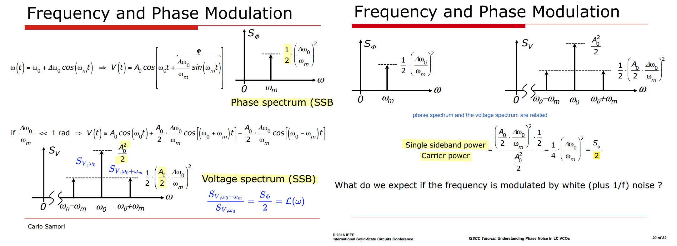
FM \(\Delta \omega_0 \cos\omega_m t\) to PM \(\frac{\Delta \omega_0}{\omega_m} \sin\omega_m t\) depend on FM modulation frequency \(\omega_m\)
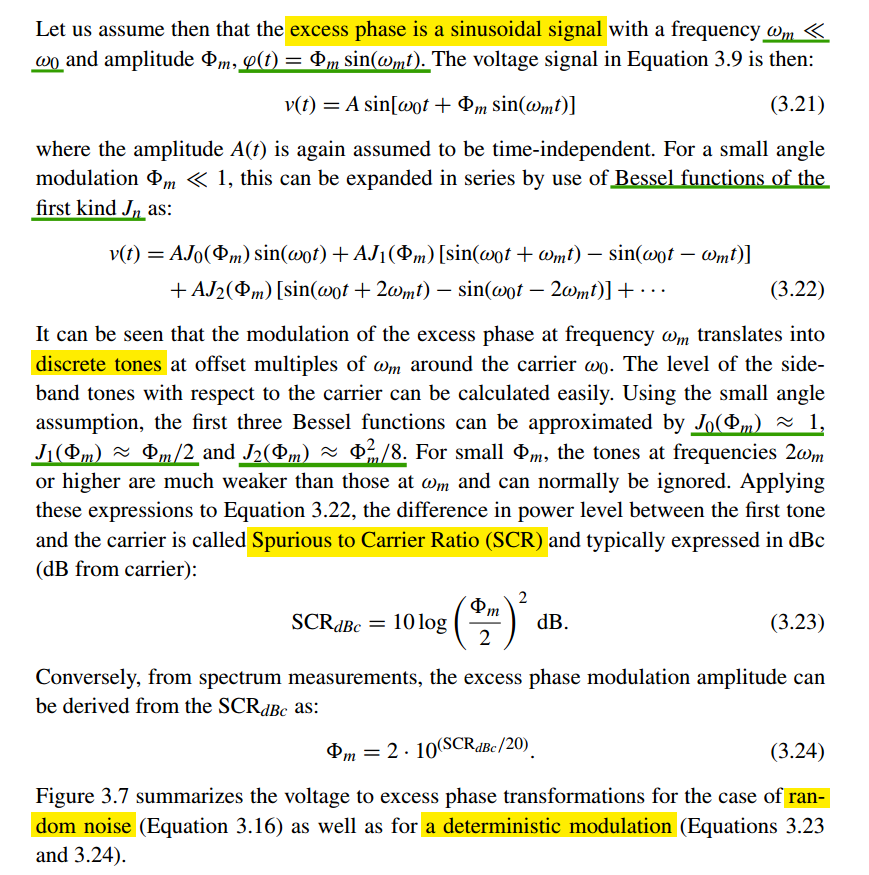
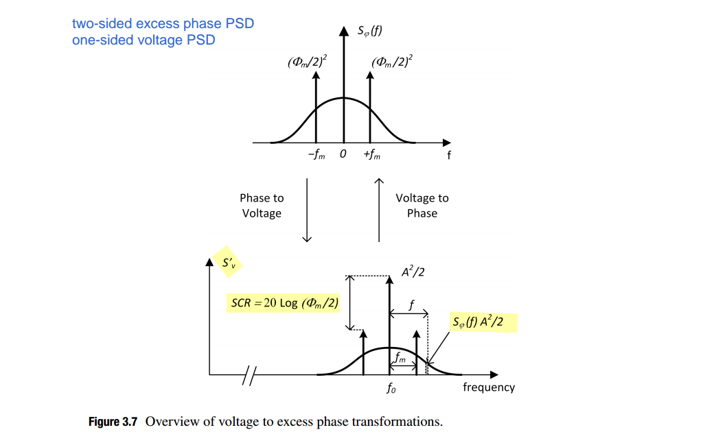
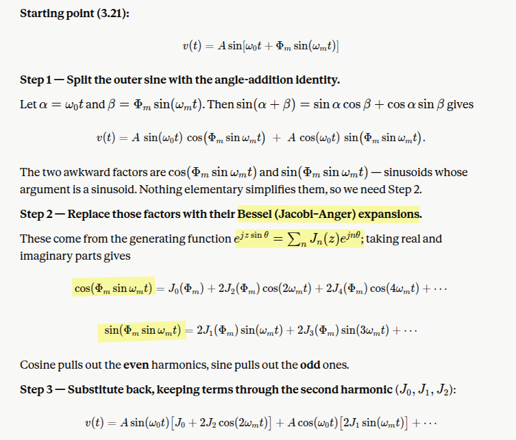
Jacobi-Anger expansions with Bessel functions
Bessel function
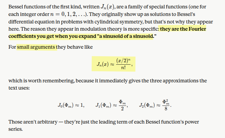
Spurious Tones in Spectrum & Spur-to-Carrier Ratio (SCR)
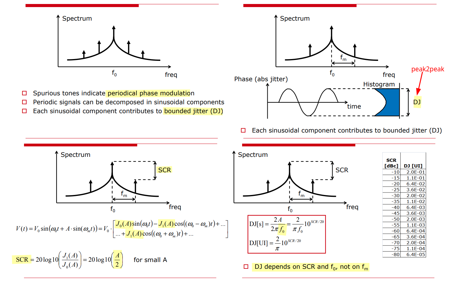
single tone PM \(A\sin\omega_m t\) to DJ don't depend on PM modulation frequency \(\omega_m\)
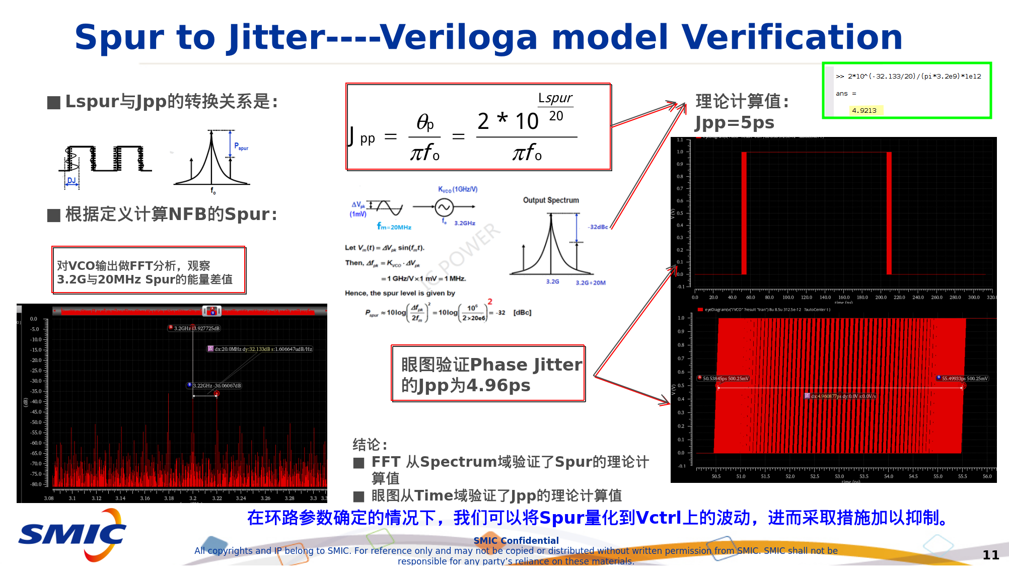
P.E. Allen - 2003 ECE 6440 - Frequency Synthesizers: Lecture 150 – Phase Noise-I [https://pallen.ece.gatech.edu/Academic/ECE_6440/Summer_2003/L150-PhaseNoise-I(2UP).pdf]
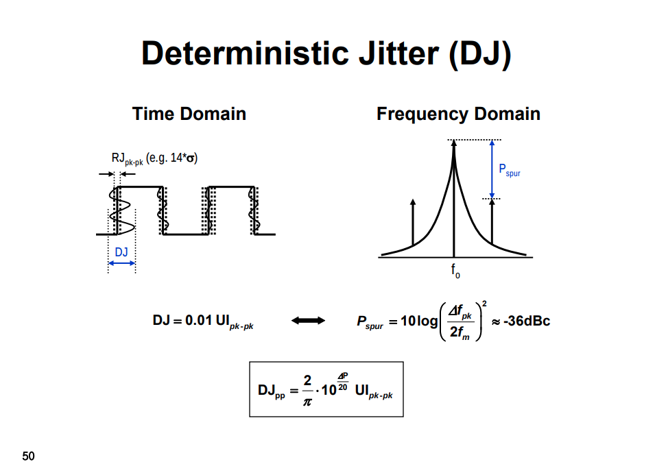 \[
f = \frac{\mathrm{d}(\omega_0 t + A\sin\omega_mt)}{2\pi
\mathrm{d}t}=\frac{\omega_0 + A\cdot 2\pi f_m \cos\omega_m t}{2\pi}
\] therefore \[
\Delta f_{pk} = Af_m
\] and \[
P_{spur} = 10\log\left(\frac{\Delta f_{pk}}{2f_m}\right)^2=
10\log\left(\frac{A}{2}\right)^2
\]
\[
f = \frac{\mathrm{d}(\omega_0 t + A\sin\omega_mt)}{2\pi
\mathrm{d}t}=\frac{\omega_0 + A\cdot 2\pi f_m \cos\omega_m t}{2\pi}
\] therefore \[
\Delta f_{pk} = Af_m
\] and \[
P_{spur} = 10\log\left(\frac{\Delta f_{pk}}{2f_m}\right)^2=
10\log\left(\frac{A}{2}\right)^2
\]
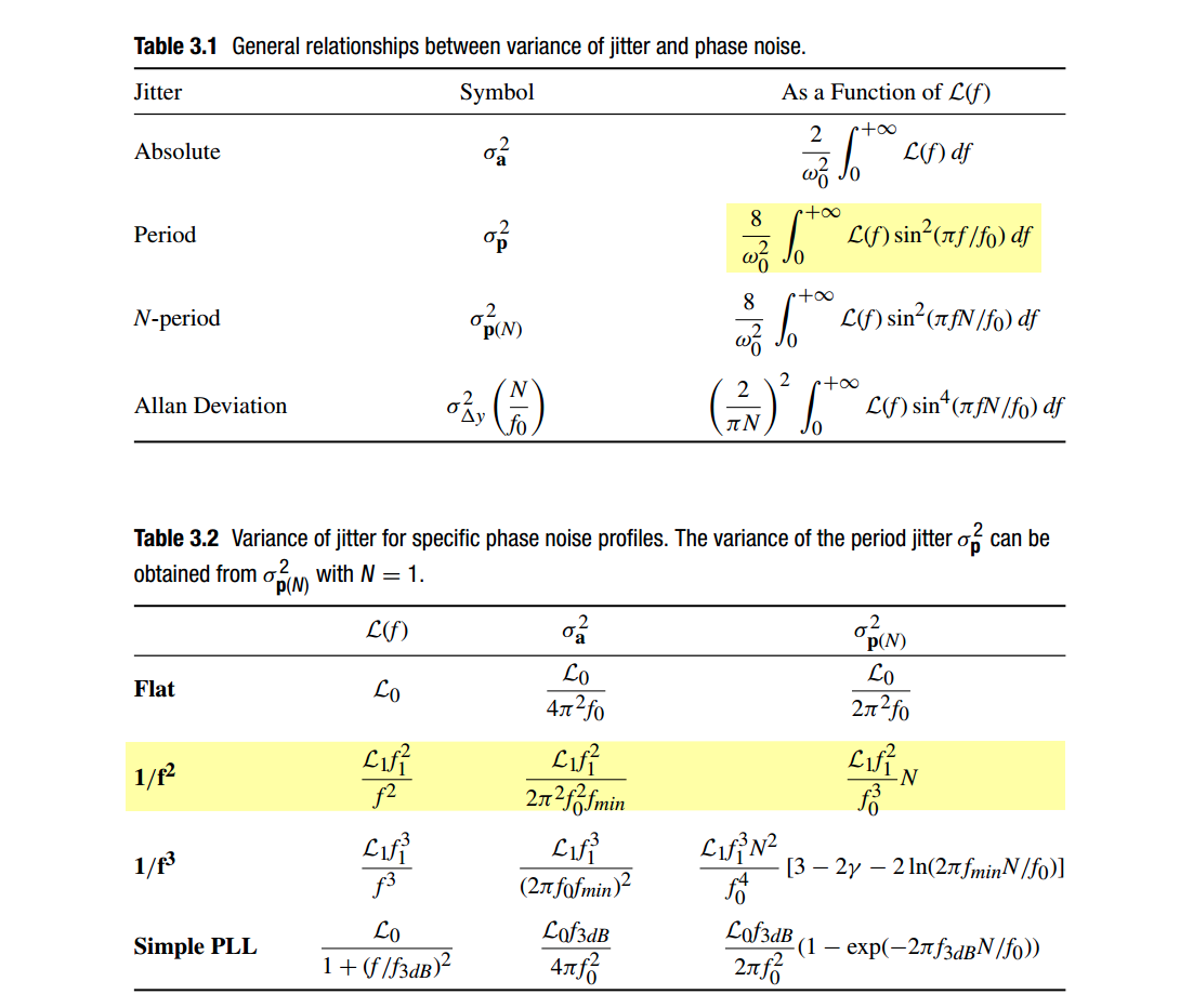
Phase Noise to Jitter
Note that \(L(f )\) is defined over positive frequencies only \((f \ge 0)\)
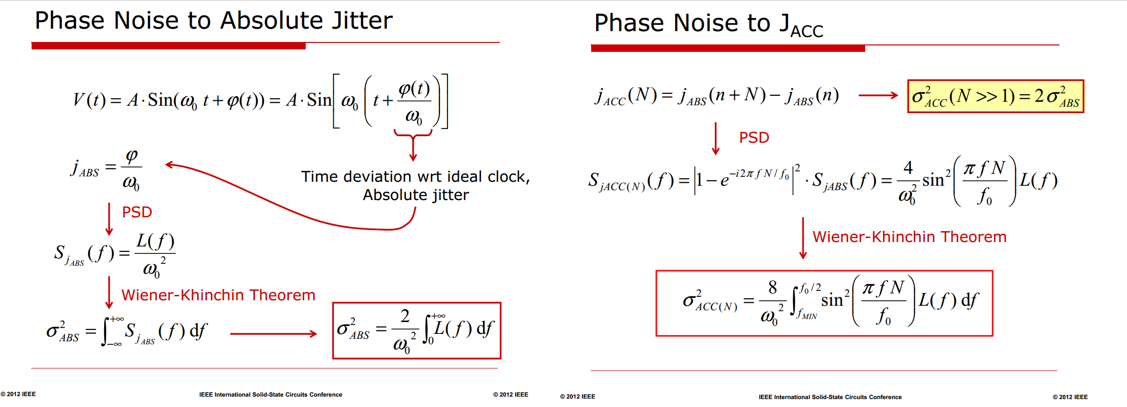 \[\begin{align}
S_{jACC(N)}(f) &= |1-z^{-N}|^2\cdot S_{jABS}(f) \\
&= |1-\cos\theta +j\sin\theta|^2\cdot S_{jABS}(f) =
((1-\cos\theta)^2 + \sin^2\theta)\cdot S_{jABS}(f) \\
&= 2(1-\cos\theta)\cdot S_{jABS}(f) = 4\sin^2(\theta/2)\cdot
S_{jABS}(f)
\end{align}\]
\[\begin{align}
S_{jACC(N)}(f) &= |1-z^{-N}|^2\cdot S_{jABS}(f) \\
&= |1-\cos\theta +j\sin\theta|^2\cdot S_{jABS}(f) =
((1-\cos\theta)^2 + \sin^2\theta)\cdot S_{jABS}(f) \\
&= 2(1-\cos\theta)\cdot S_{jABS}(f) = 4\sin^2(\theta/2)\cdot
S_{jABS}(f)
\end{align}\]
where \(\theta = 2\pi f N/f_0\)
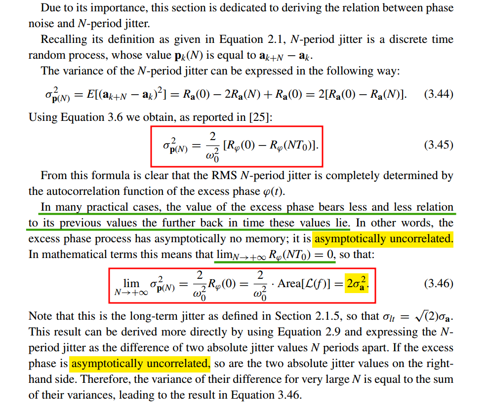
As EQ(3.44), EQ(3.45)
the autocorrelation is the inverse Fourier transform of the PSD
\[ R_{\varphi}(t) = \int_{-\infty}^{+\infty} S_{\varphi} (f) e^{j2\pi f t}df \]
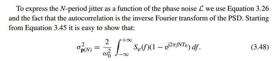
Then, \[ R_{\varphi}(0) = \int_{-\infty}^{+\infty} S_{\varphi} (f) df \qquad R_{\varphi}(NT_0) = \int_{-\infty}^{+\infty} S_{\varphi} (f) e^{j2\pi f NT_0} df \] Thus, yield EQ(3.48)
Simplified PLL Phase Noise Profile
Absolute Jitter
TODO 📅
Period Jitter
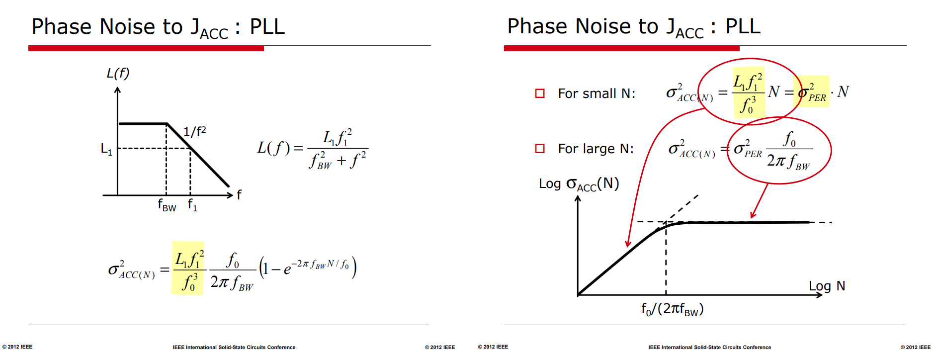
Given Simple PLL \(\frac{\mathcal{L}_0}{1 + (f / f_{3dB})^2}\) and \(\sigma_{p(N)}^2=\frac{\mathcal{L}_0 f_{3dB}}{2\pi f_0^2} \left(1 - \exp\left(-2\pi f_{3dB} N / f_0\right)\right)\)
| \(1 - \exp\left(-2\pi f_{3dB} N / f_0\right)\) | \(\sigma_{\mathbf{p}(N)}^2\) | |
|---|---|---|
| small \(N\) | \(\frac{2\pi f_{3dB} N} {f_0}\) | \(\sigma_{PER}^2\cdot N\) |
| large \(N\) | \(1\) | \(\sigma_{PER}^2\cdot \frac{f_0}{2\pi f_{3dB}}\) |
where \(\sigma_{\mathbf{p}}^2 = \frac{\mathcal{L}_0 f_{3dB}^2}{f_0^3}\)
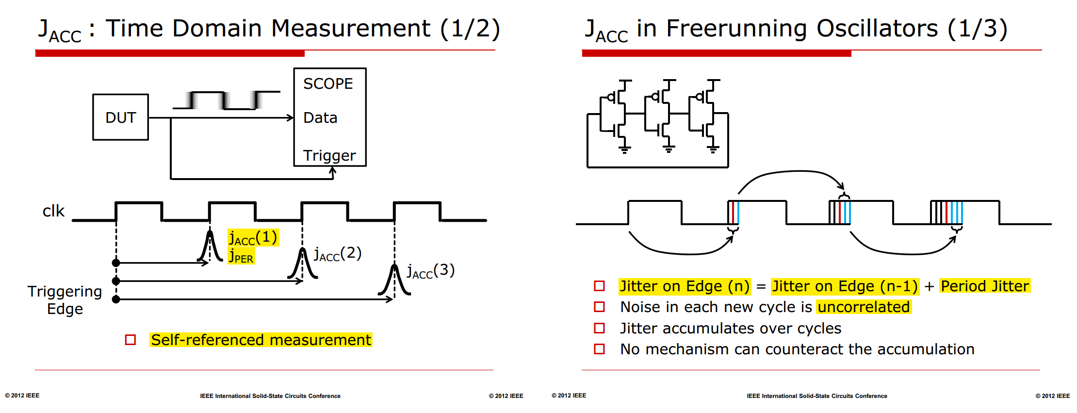
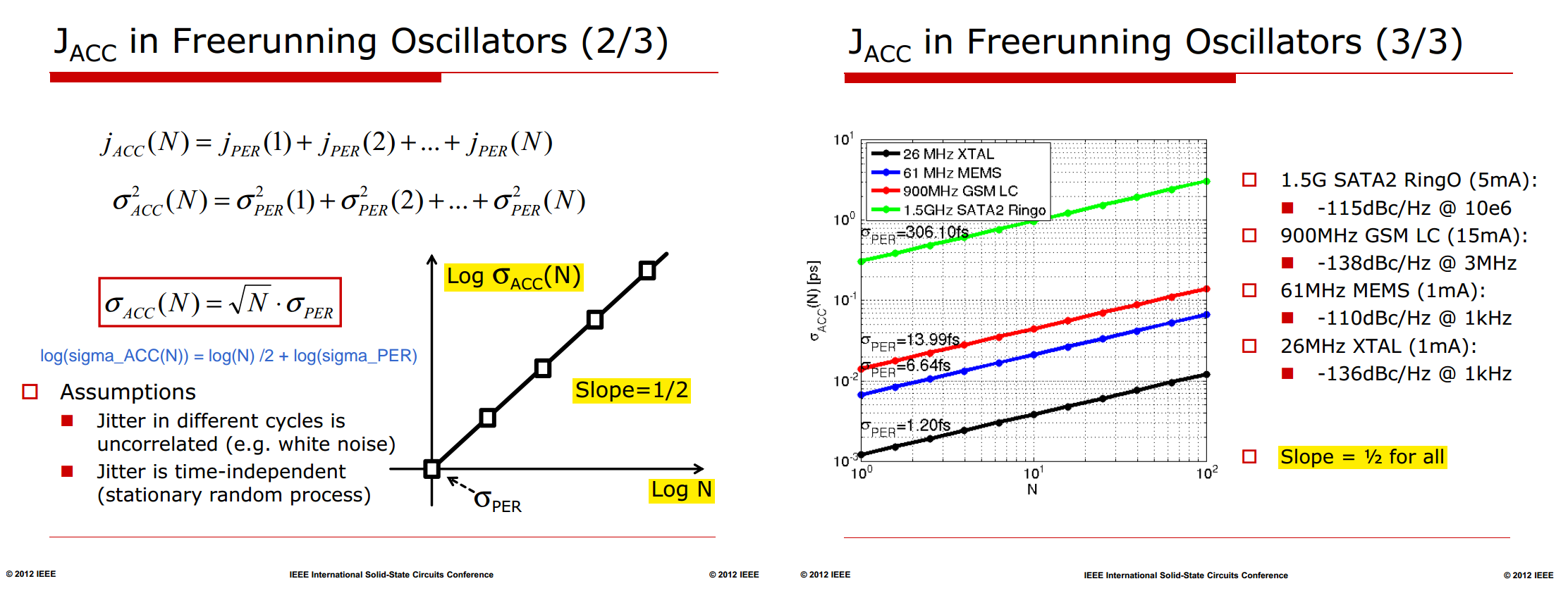
a random-walk DCO - \(1/f^2\) Phase Noise Profile
L. Avallone, M. Mercandelli, A. Santiccioli, M. P. Kennedy, S. Levantino and C. Samori, "A Comprehensive Phase Noise Analysis of Bang-Bang Digital PLLs," in IEEE Transactions on Circuits and Systems I: Regular Papers, vol. 68, no. 7, pp. 2775-2786, July 2021 [https://sci-hub.st/10.1109/TCSI.2021.3072344]

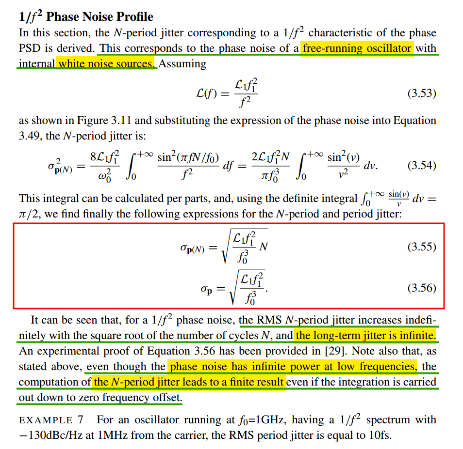
Mozhgan Mansuri “Low-Power Low-Jitter On-Chip Clock Generation” thesis UCLA [https://people.engr.tamu.edu/spalermo/ecen689/pll_thesis_mansuri_ucla_2003.pdf]
[https://people.engr.tamu.edu/spalermo/ecen689/PRBS_&_PLL_model.pdf]
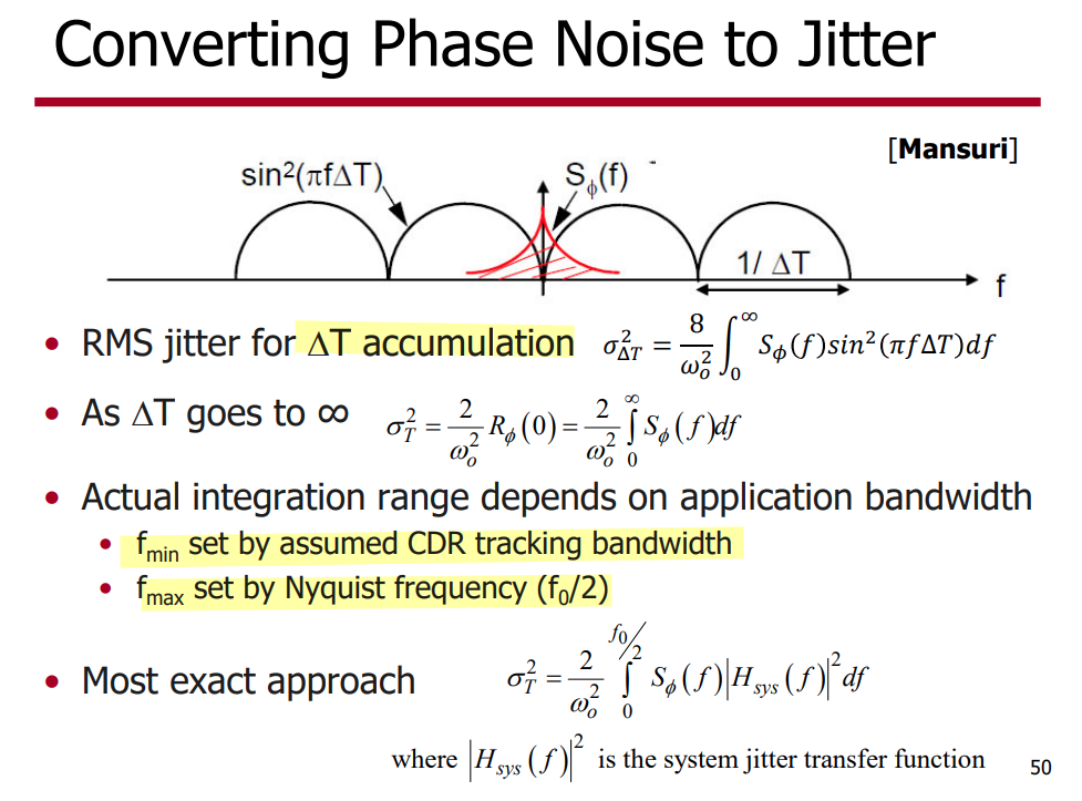
\(1/f^2\)$ phase noise corresponds to white frequency/period fluctuations
- \(L(f) \propto \frac{1}{f^2}\) phase noise corresponds to white frequency noise.
- Frequency/period fluctuations are related to the derivative of phase, introducing an \(f^2\) factor.
Therefore:
\[ S_{\phi}(f) \propto \frac{1}{f^2} \quad\Rightarrow\quad S_{\Delta f}(f) \propto f^2 S_{\phi}(f) = \text{constant} \]
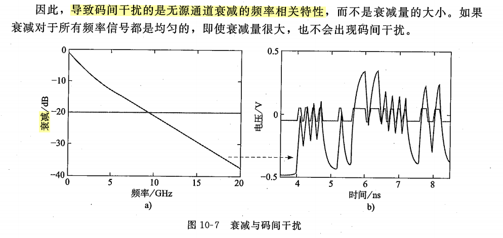
Intersymbol interference (ISI)

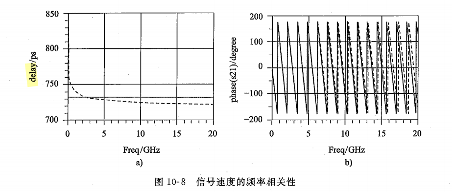

\[ \color{red}\phi = 2\pi D \cdot f \]
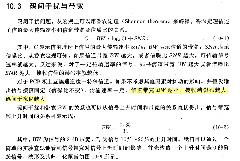
Even-odd Jitter (EOJ)
| Jitter measurement | Description |
|---|---|
| F/2 | F/2 is the peak-to-peak amplitude of the periodic jitter occurring at 1/2 of the data rate. |
Even-odd jitter, also known as F/2 jitter, arises from a clock signal's duty cycle not being perfectly 50%
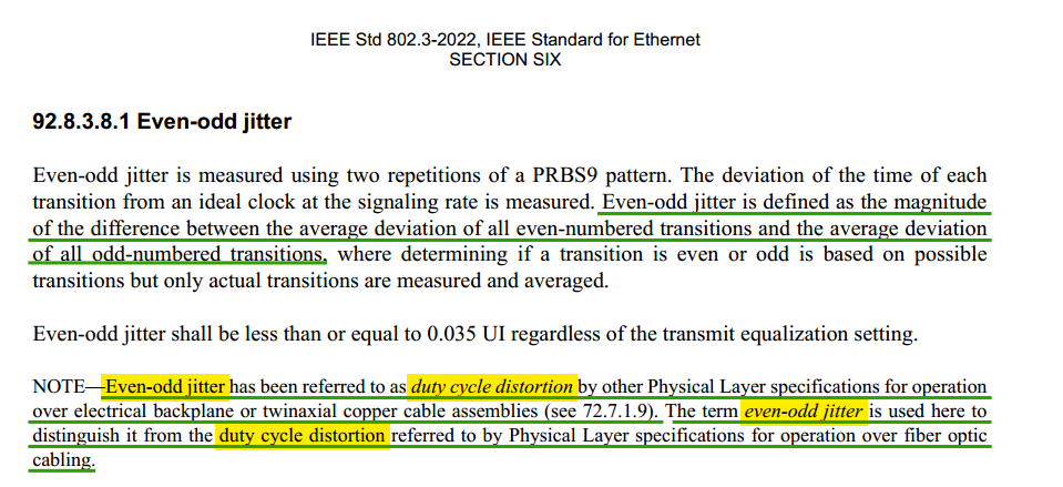
Even-odd jitter has been referred to as duty cycle distortion by other Physical Layer specifications for operation over electrical backplane or twinaxial copper cable assemblies
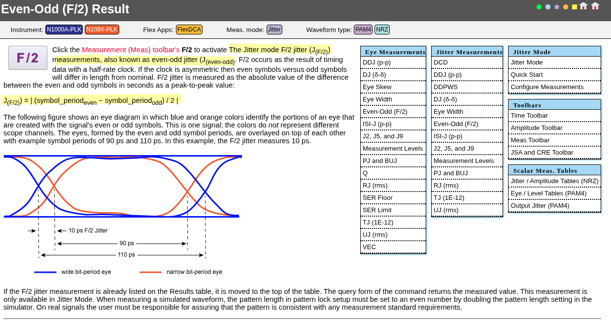
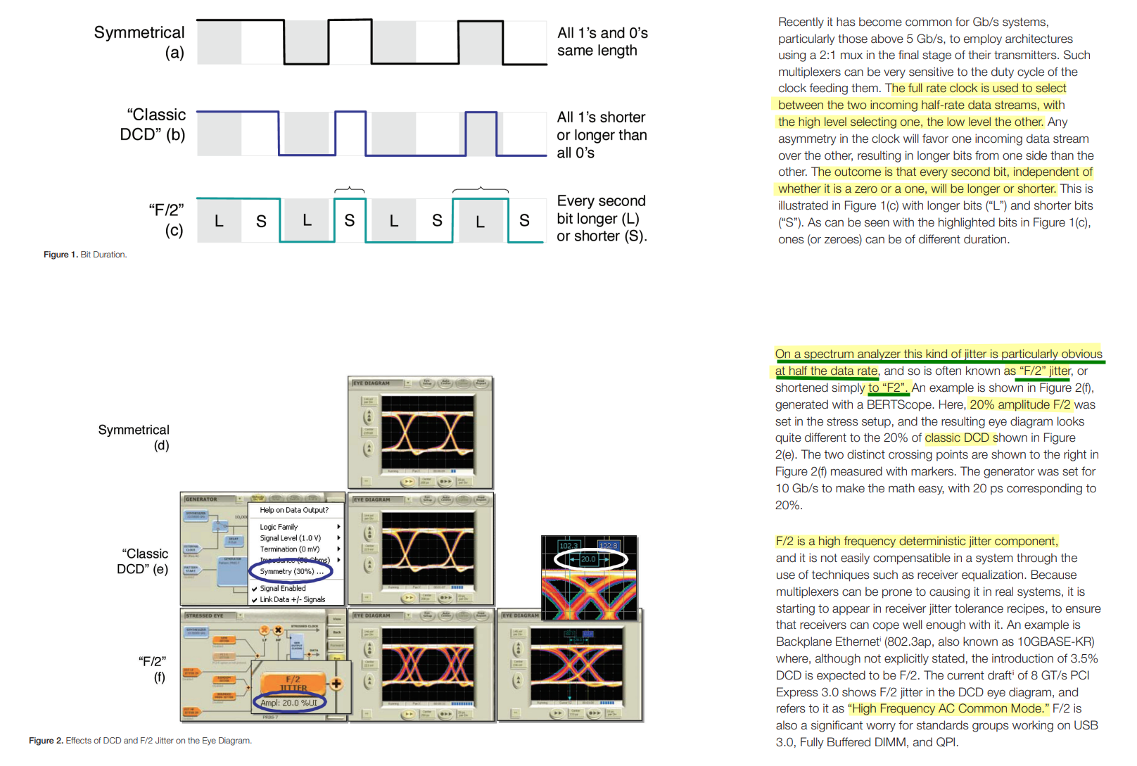
Comparing DCD and F/2 Jitter Using a BERTScope® Bit Error Rate Testing Application Note [https://download.tek.com/document/65W_26040_0_Letter.pdf]
Pulse Width Jitter (PWJ)
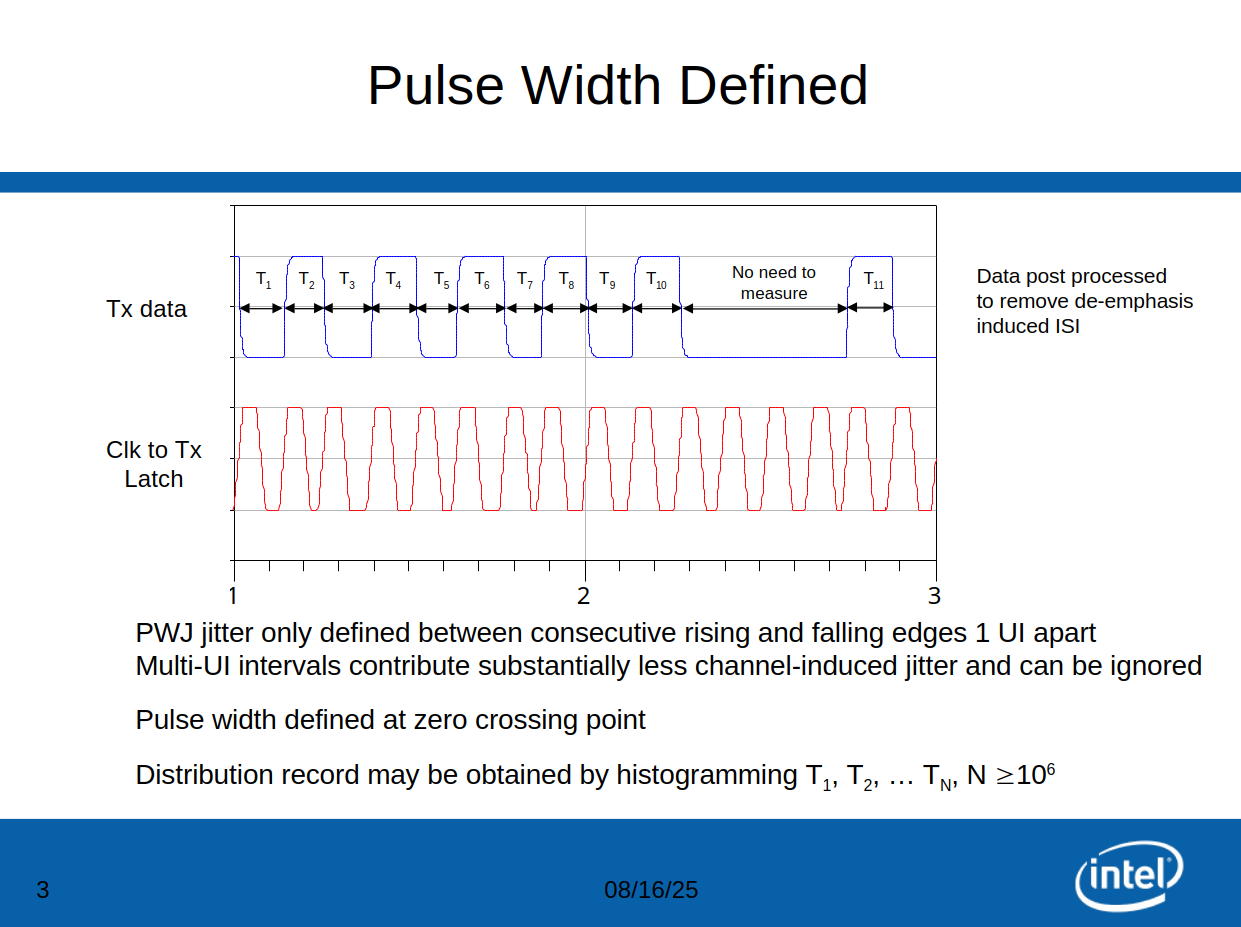
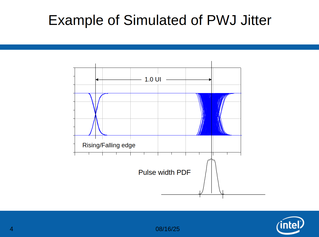
Jeff Morriss Updated 10/25/07. Analysis of 8G PCIe Pulse Width Jitter (UI to UI Jitter_10_25.ppt)
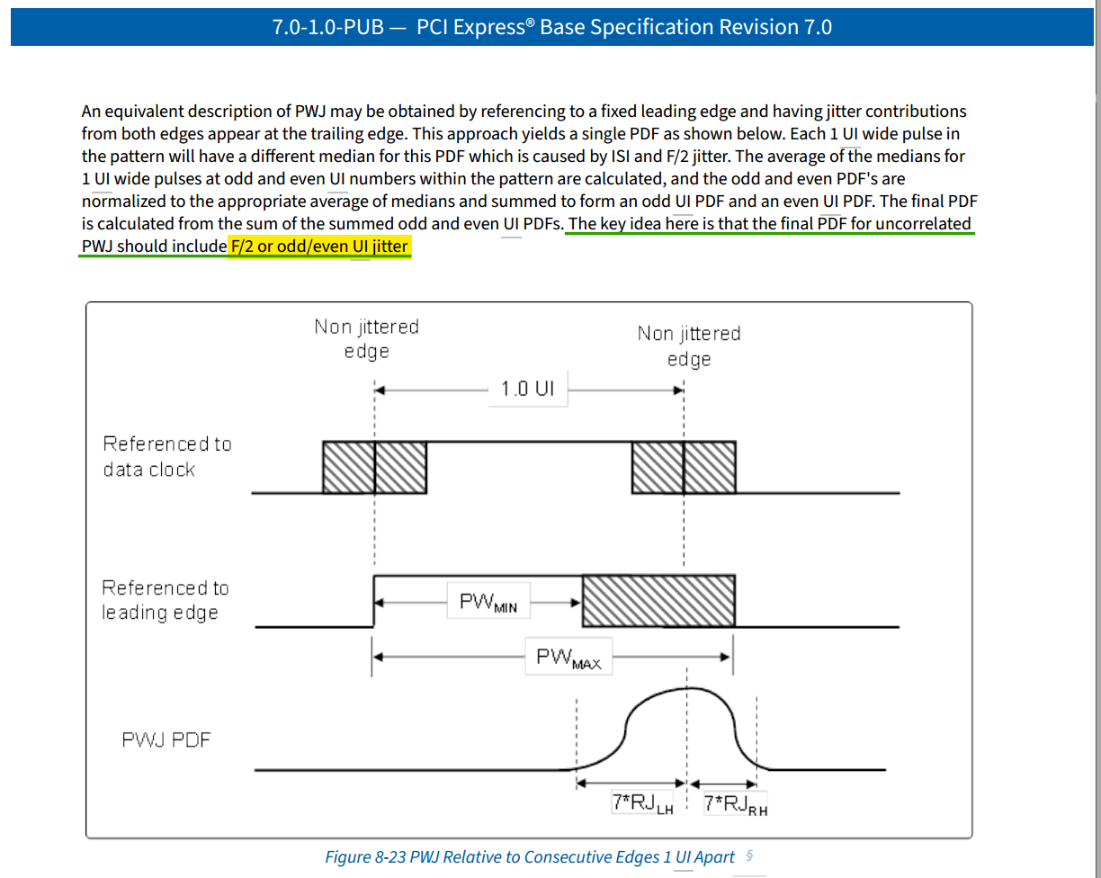
Duty Cycle Distortion (DCD)
DCD peak to peak jitter #2 [https://github.com/LewisLiuLiuLiu/SerDesSystemCProject/issues/2] [Commit 1723ee6]
 \[
\boxed{\text{DJ}_{\text{DCD,pp}} = 2 \times \text{UI} \times \left|
\text{DCD}\% - 50\% \right|}
\]
\[
\boxed{\text{DJ}_{\text{DCD,pp}} = 2 \times \text{UI} \times \left|
\text{DCD}\% - 50\% \right|}
\]
1 | docs: correct DCD-induced jitter formula to 2·|DCD%−50%|·UI (EN/zh) |
| Jitter measurement | Description |
|---|---|
| DCD | Duty Cycle Distortion is the peak-to-peak amplitude of the component of the deterministic jitter correlated with the signal polarity. |
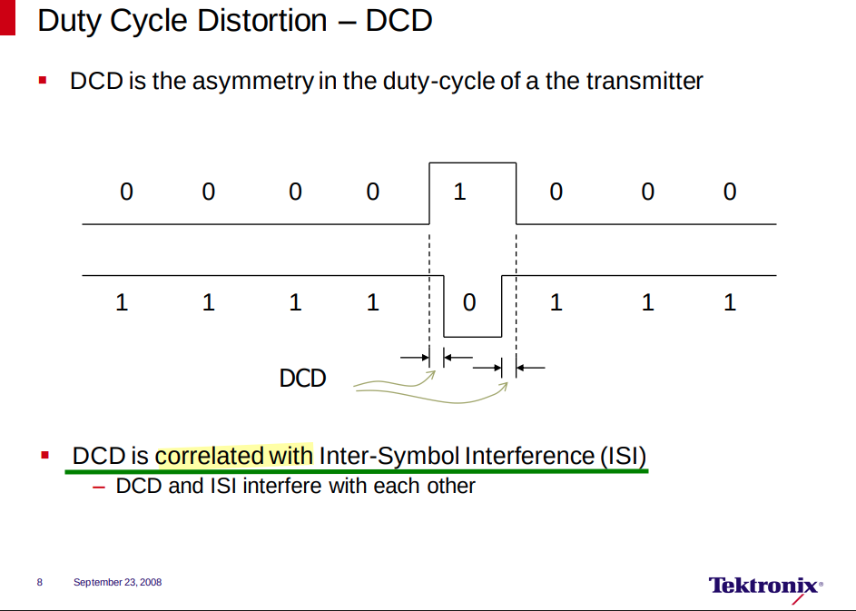
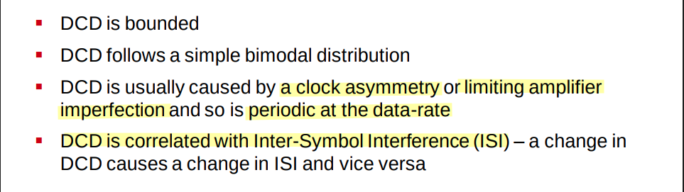
Jitter fundamental & How Isolating Root Causes of Jitter [https://picture.iczhiku.com/resource/eetop/ShKgzTEiUfdFOcvn.pdf]
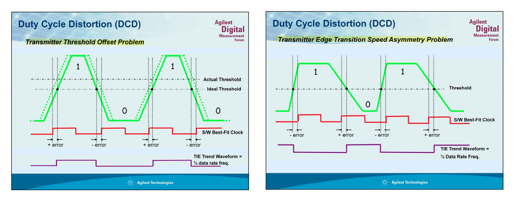
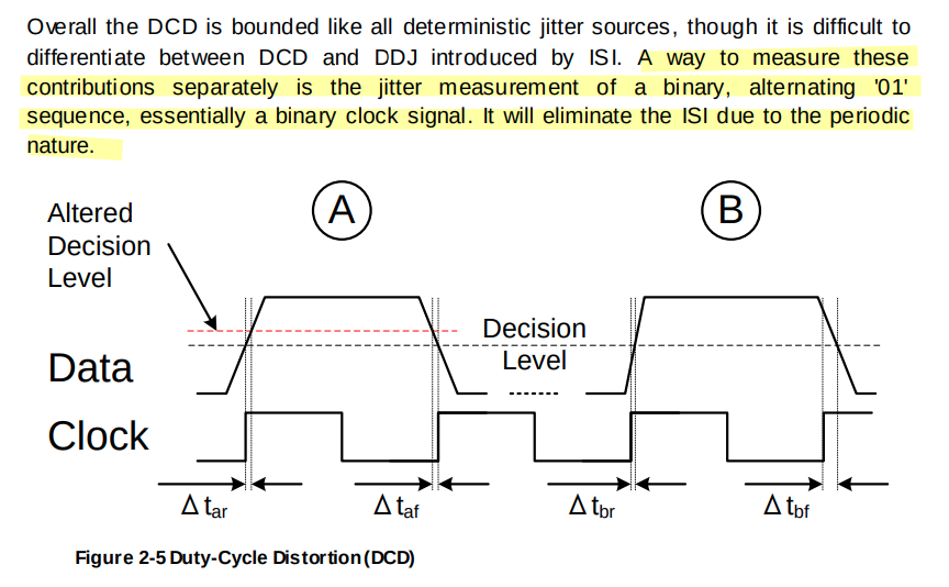
There are two primary causes of DCD jitter which are usually generated within a transmitter
- If the data input to a transmitter is theoretically perfect, but if the transmitter sampling threshold is offset from its ideal level, then the output of transmitter will have duty cycle distortion as a function of the slew rate of the data signal
- Another cause of duty cycle distortion can be a mismatch/asymmetry in rising and falling edge speeds
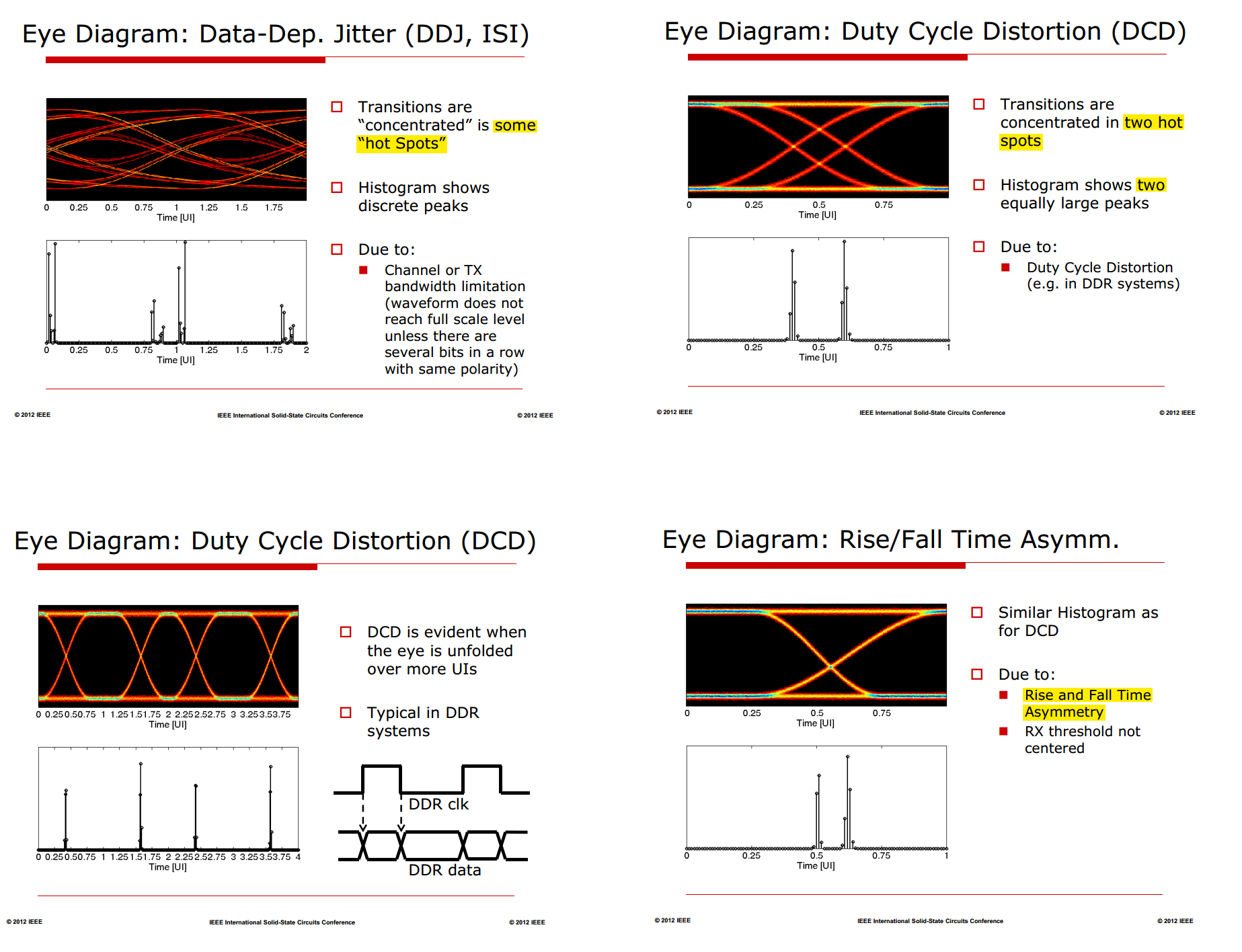
Unfortunately, other sources such as ISI almost always exist making
it sometimes difficult to isolate the DCD component. One technique to
test for DCD is to stimulate your system/components with a
repeating 1-0-1-0… data pattern. This
technique will eliminate inter-symbol interference (ISI) jitter and make
viewing the DCD within the spectrum display much easier
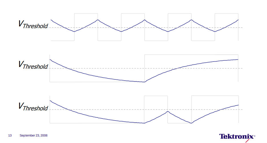
Why clock pattern? That's because all symbols experience same inter-symbol interference, which are canceled out
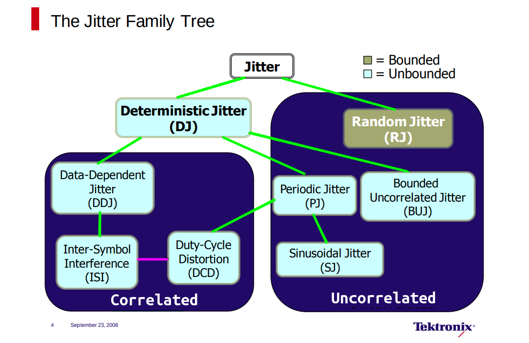
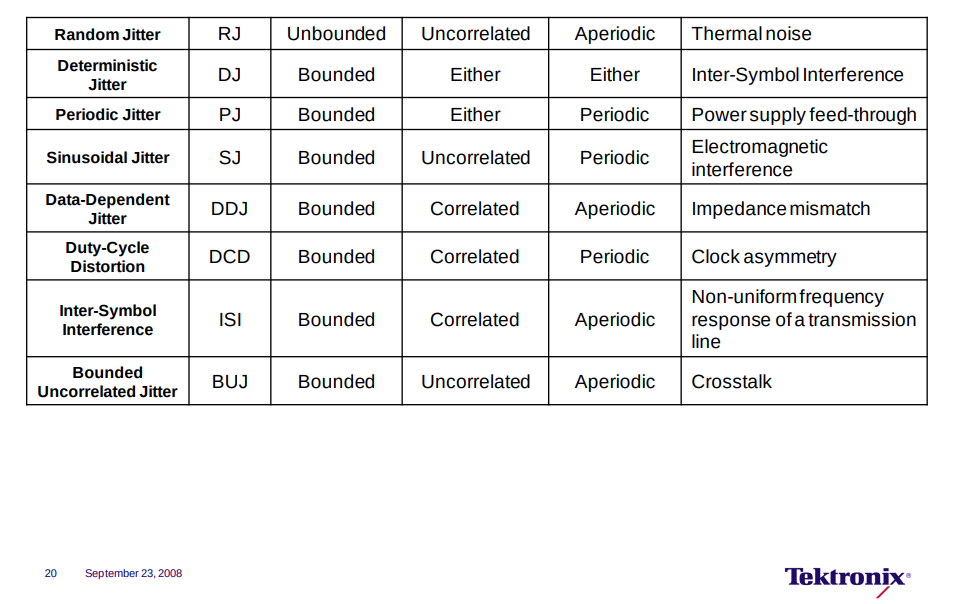
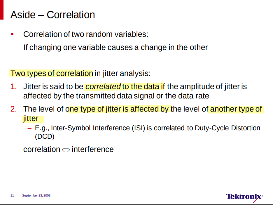
Correlated vs. Uncorrelated
If the PDF of one jitter source changes when the PDF of another source is changed, then those two sources are dependent or correlated
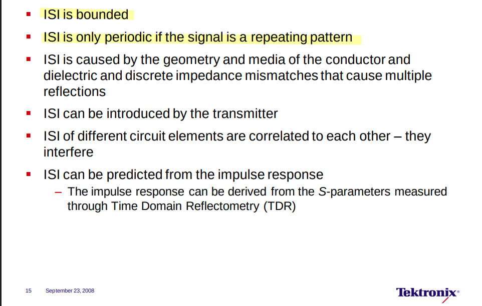
Inter-Symbol Interference (ISI)
The primary cause of Data Dependent Jitter
Jitter measurements can be classified into three categories: cycle-to-cycle jitter, period jitter, and long-term jitter
Jitter is a key performance parameter. Need to know what matters in each case:
- PJ for digital timing
- LTJ for data converters and serial data
- Phase noise for communications (not all bandwidths matter)
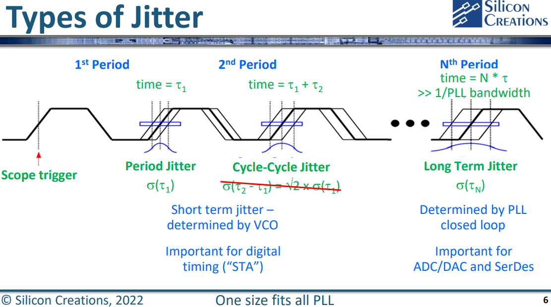
The above Cycle-Cycle Jitter equation is wrong, \(\tau_1\) and \(\tau_2\) are not independent
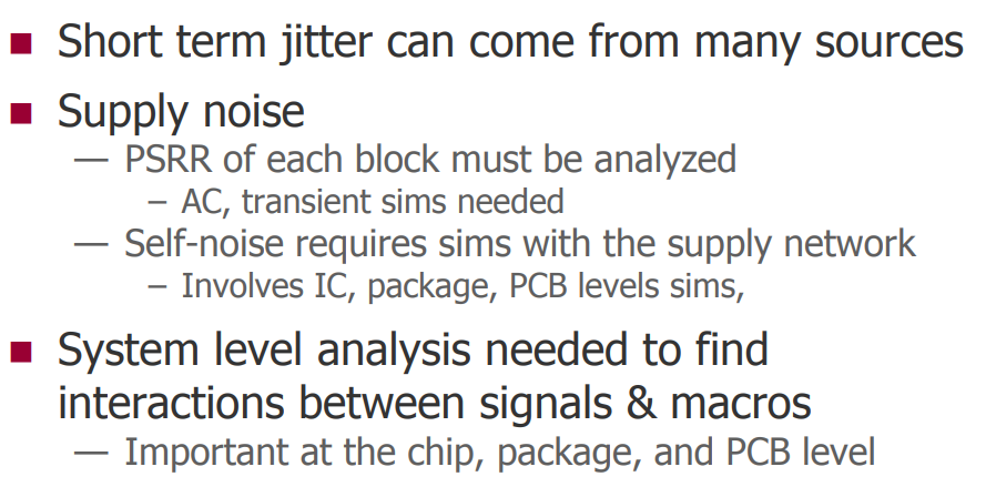
Short Term Jitter
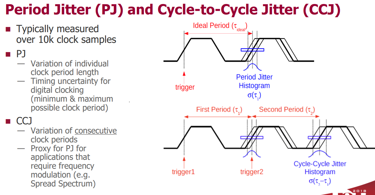
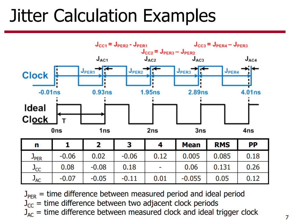
Period jitter, Jper is the short term variation in clock period compared to the average (mean) clock period.
Cycle-to-Cycle, Jcc is the time difference of two adjacent clock periods
Long Term Jitter (LTJ)
[https://people.engr.tamu.edu/spalermo/ecen689/PRBS_&_PLL_model.pdf]
absolute jitter is also known as long-term jitter
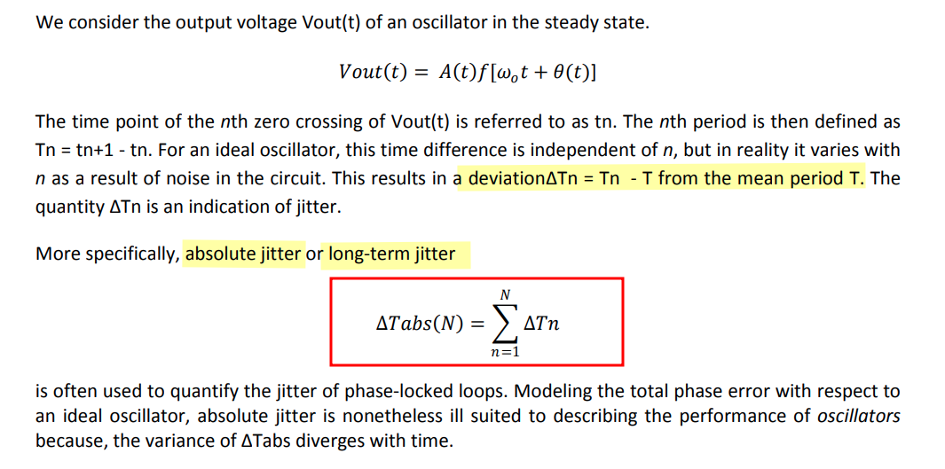
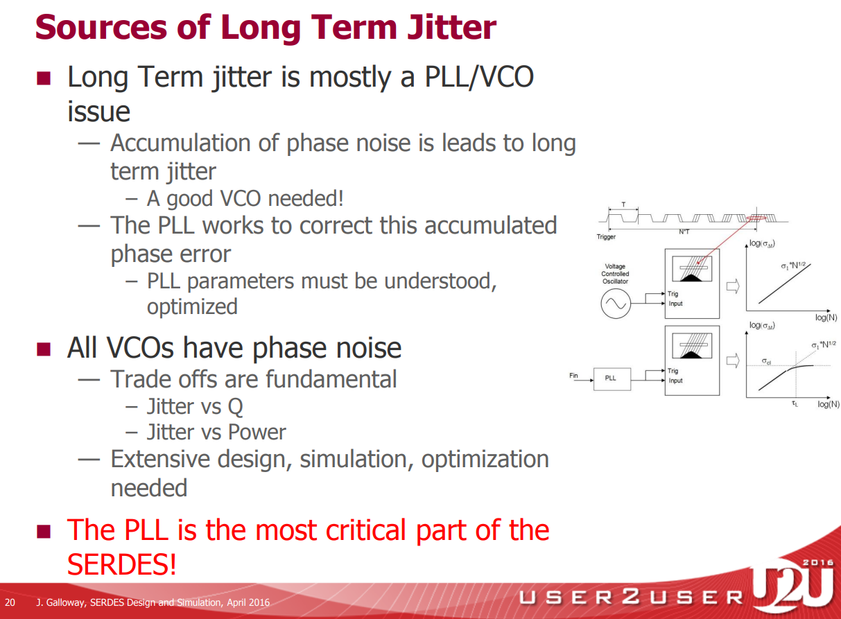
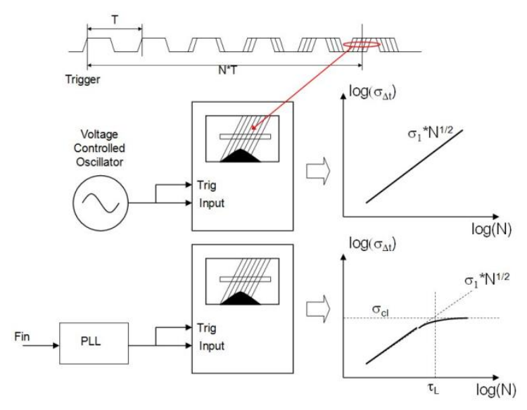
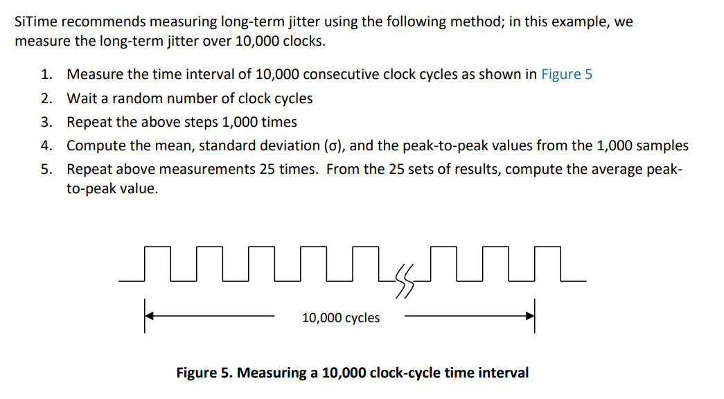
measuring LTJ
Jitter Calculation Examples
Jcc vs Jper
Estimating the RMS cycle-to-cycle jitter if all you have available is the RMS period jitter.
- Cycle-to-cycle jitter - The short-term variation in clock period between adjacent clock cycles. This jitter measure, abbreviated here as \(J_{CC}\), may be specified as either an RMS or peak-to-peak quantity.
- Period jitter - The short-term variation in clock period over all measured clock cycles, compared to the average clock period. This jitter measure, abbreviated here as \(J_{PER}\), may be specified as either an RMS or peak-to-peak quantity.
Let the variable below represent the variance of a single edge's timing jitter, i.e. the difference in time of a jittery edge versus an ideal edge, \(\sigma^2_j\)
If each edge's jitter is independent then the variance of the period jitter can be written as \[\begin{align} \sigma^2_\text{jper} &= (\sigma_\text{j(n+1)}-\sigma_\text{j(n)})^2 \\ &= \sigma_\text{j(n+1)}^2-2\sigma_\text{j(n+1)}\sigma_\text{j(n)})+\sigma_\text{j(n)})^2\\ &= \sigma_\text{j(n+1)}^2+\sigma_\text{j(n)})^2 \\ &=2\sigma^2_j \end{align}\]
In every cycle-to-cycle measurement we use one "interior" clock edge twice and therefore we must account for this
\[\begin{align} \sigma^2_\text{jcc} &= (\sigma_\text{jper(n+1)}-\sigma_\text{jper(n)})^2 \\ &=(\sigma_\text{j(n+2)}-2\sigma_\text{j(n+1)}+\sigma_\text{j(n)})^2 \end{align}\]
Since each edge's jitter is assumed to be independent and have the same statistical properties we can drop the cross correlation terms and write:
\[\begin{align} \sigma^2_\text{jcc} &=(\sigma_\text{j(n+2)}-2\sigma_\text{j(n+1)}+\sigma_\text{j(n)})^2 \\ &=\sigma_\text{j(n+2)}^2+4\sigma_\text{j(n+1)}^2+\sigma_\text{j(n)}^2 \\ &=6\sigma_\text{j}^2 \end{align}\]
The ratio of the variances is therefore \[ \frac{\sigma^2_\text{jcc}}{\sigma^2_\text{jper}} = \frac{6\sigma_\text{j}^2} {2\sigma_\text{j}^2}=3 \] Then \[ \sigma_\text{jcc} = \sqrt{3}\sigma_\text{per} \]
[Timing 101 #8: The Case of the Cycle-to-Cycle Jitter Rule of Thumb, Silicon Labs]
Phase Noise Modeling
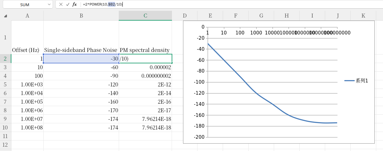
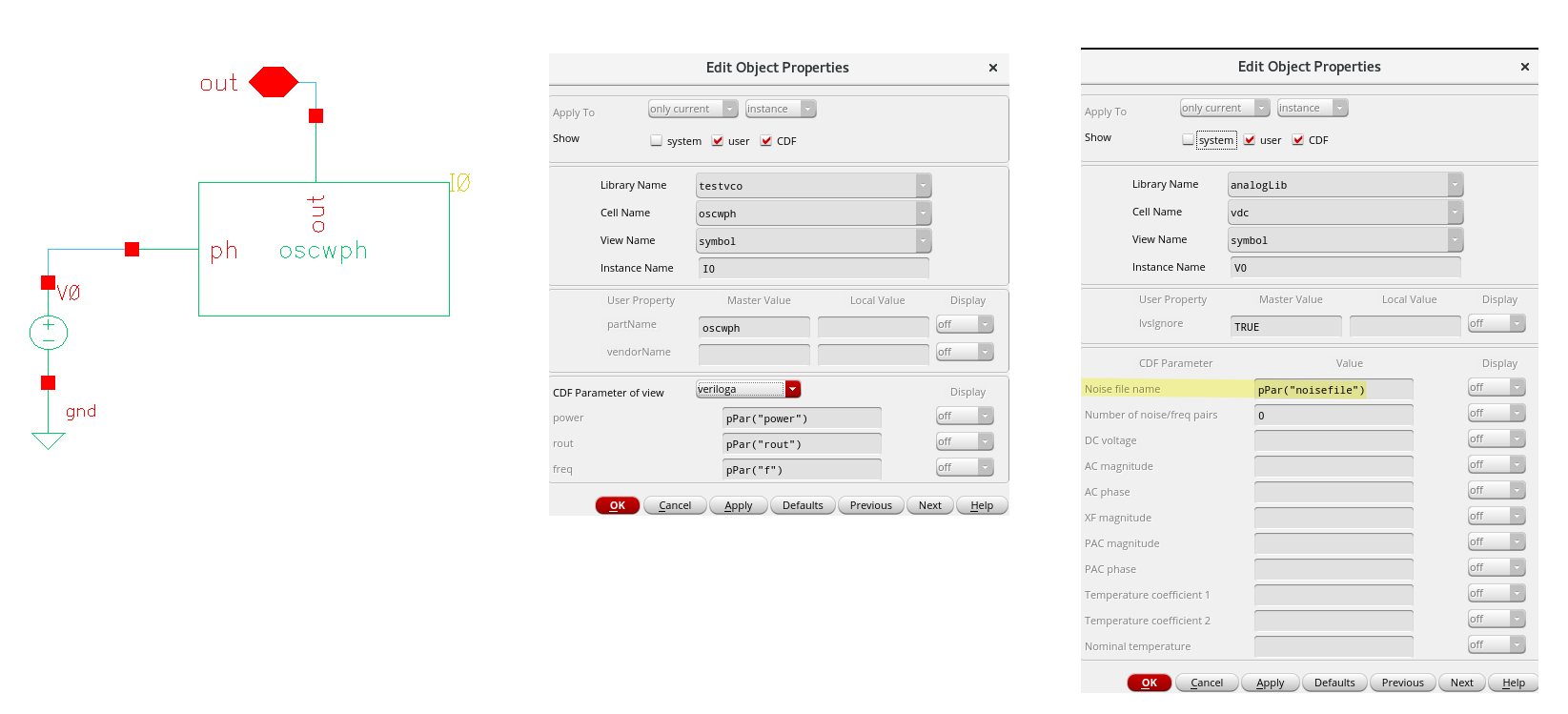
w/ noisefile
Tawna, "Modeling Oscillators with Arbitrary Phase Noise Profiles"[https://community.cadence.com/cadence_blogs_8/b/rf/posts/modeling-oscillators-with-arbitrary-phase-noise-profiles]
—, "How to Specify Phase Noise as an Instance Parameter in Spectre Sources (e.g. vsource, isource, Port)" [https://community.cadence.com/cadence_blogs_8/b/rf/posts/how-to-specify-phase-noise-as-an-instance-parameter-in-spectre-sources-e-g-vsource-isource-port]
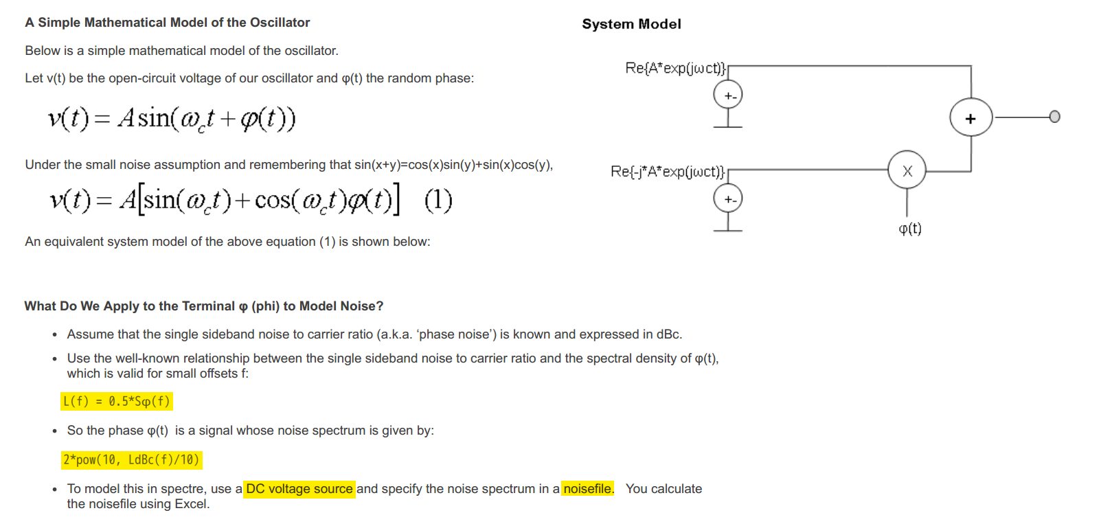
driving an otherwise ideal oscillator with direct phase modulation makes its noise purely PM — a good model of near-carrier oscillator noise
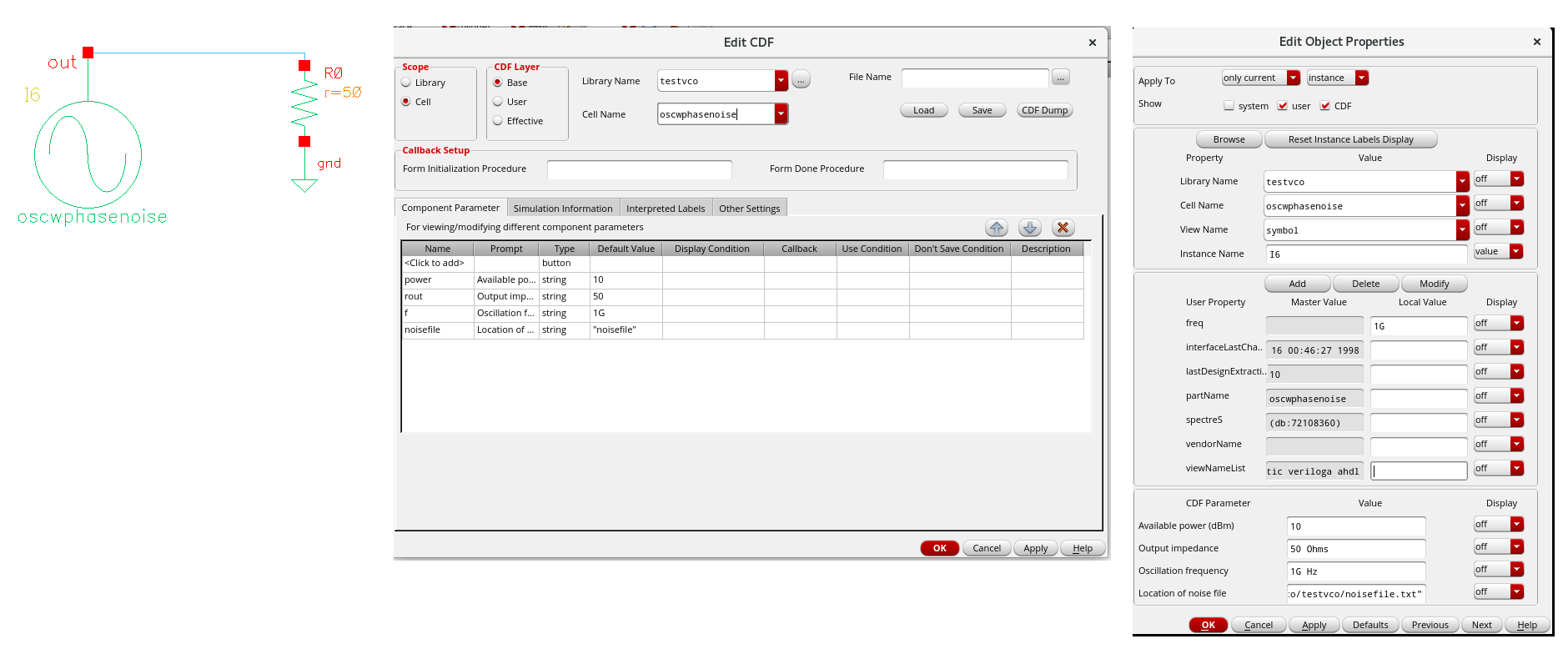
In verilog-A model oscwphnoise.va,
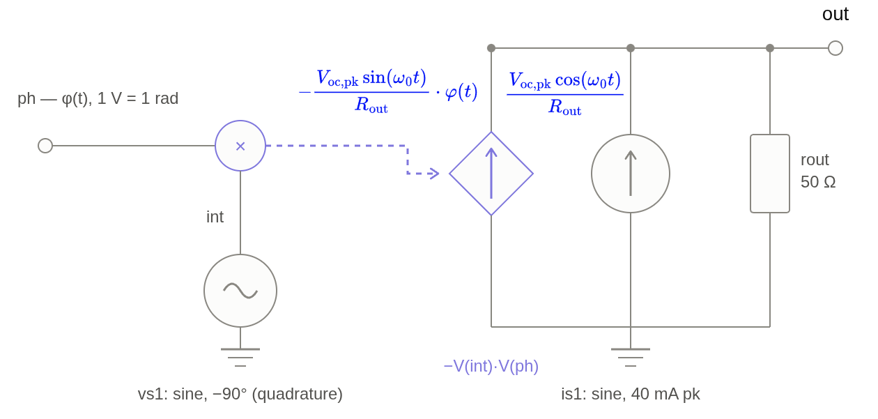
Norton-equivalent circuit \[
\boxed{v(t) = A\cos(\omega_0 t + \phi(t))\approx A[\cos\omega_0 t -
\sin\omega_0 t \cdot \varphi(t)]}
\] 
1 |
The first two macros convert the available power from dBm to watts: \[ P_{\mathrm{W}} = 10^{(P_{\mathrm{dBm}}-30)/10}. \] The third macro calculates the open-circuit peak voltage \[ V_{\text{oc,pk}}=\sqrt{8R_{\text{out}}P_{\mathrm{W}}}. \] The factor \(8\) follows from a matched source: \[ V_{\text{load,pk}}=\frac{V_{\text{oc,pk}}}{2}, \] and therefore \[ P_{\mathrm{avail}} = \frac{V_{\text{load,rms}}^2}{R_{\text{out}}} = \frac{\left(V_{\text{oc,pk}}/2\sqrt{2}\right)^2}{R_{\text{out}}} = \frac{V_{\text{oc,pk}}^2}{8R_{\text{out}}}. \] For the defaults, \[ P=10\ \mathrm{dBm}=10\ \mathrm{mW}, \qquad R_{\text{out}}=50\ \Omega, \] so \[ V_{\text{oc,pk}} = \sqrt{8(50)(0.01)} = 2\ \mathrm{V}. \] With a matched \(50\ \Omega\) load, the load voltage is \(1\ \mathrm{V_{pk}}\), corresponding to \(10\ \mathrm{dBm}\).
1 |
|
Note that int is purely internal — no current flows
there, and it never appears at the output; vs1 exists only
to be sampled by the multiplier
isource and vsource are not
built-in Verilog-A language constructs. They are
Cadence-provided behavioral source modules \[
\boxed{
\texttt{isource},\ \texttt{vsource}
\text{ are instantiated source models supplied by Cadence}
}
\]
- vsource (p, n) forces V(p) − V(n) = w(t), where for
type="sine"the waveform is w(t) = ampl·sin(2πf(t − delay) + sinephase·π/180), withsinephasein degrees.
So in the model, vs1(gnd, int) means V(gnd) − V(int) =
w(t), i.e. V(int) = −w(t) — the polarity flips because
ground was listed first.
- isource (p, n): positive current flows from p, through the source, to n — it is pulled out of node p and injected into node n.
So is1(gnd, out) pumps ampl·sin(ωt) into node
out, which is exactly why the blog wired it as (gnd, out):
to drive the output. Writing is1(out, gnd) with the same
amplitude would sink that current from out instead
I(a,b) <+ expradds a currentexprflowing a → b through that branch.
So I(out) <+ V(out)/rout is a
resistor from out to ground,
and **I(out) <+ -X** injects X into
out (positive contribution = current leaving the node)
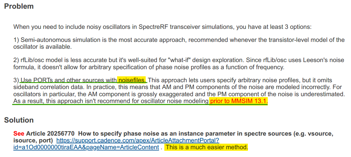
For modern spectreRF, PORTs and other sources with noisefiles or instance parameter are easier and correct methods
Starting in MMSIM 13.1, you can specify the phase noise as an instance parameter in Spectre sources, including port, vsource and isource
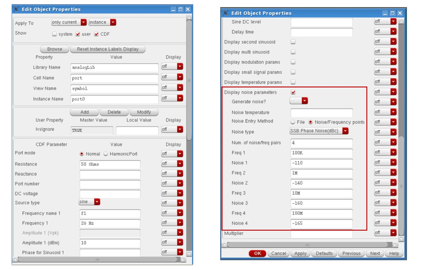
The Generate noise? button (corresponds to
isnoisy parameter on the port) is by default set to
"yes"
w/ periodic jitter inject
我想流tsmc28nm, 振荡器噪声建模:从Phase Noise 到Jitter [xiaohongshu]
Claude Fable5 [Github gist]
Matthew Schubert. Colouring Noise - Generating coloured noise to simulate physical processes [https://blog.ioces.com/matt/posts/colouring-noise/] [https://gist.github.com/m-schubert/45c562146c6607b8990f1e8f34ff87b0]
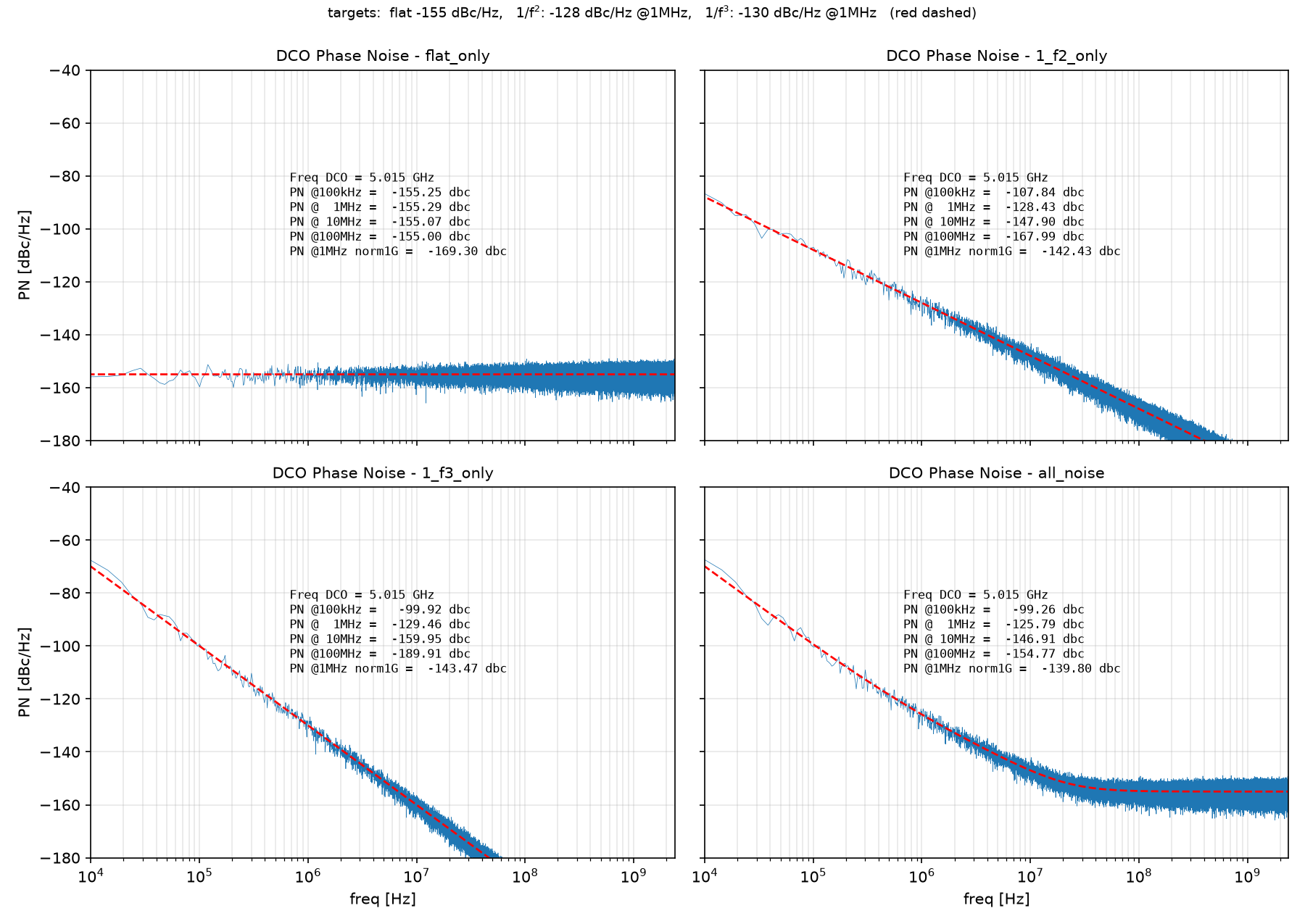
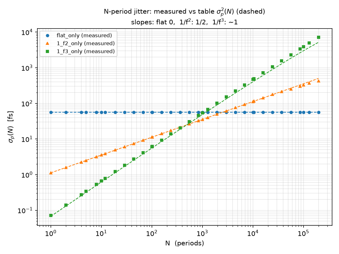
The same jitter standard deviation \(\sigma_a^2\) can correspond to completely different phase noise shapes. A single \(\sigma_a^2\) cannot define the PN shape, because σ is an integral of the spectrum, and integration throws away shape information.
The shape lives in the correlation structure of the jitter sequence — equivalently, in how \(\sigma^2_{p(N)}\) grows with \(N\) — and in your simulation it is set by how you generate and inject the samples, not by the \(\sigma_a^2\) value itself
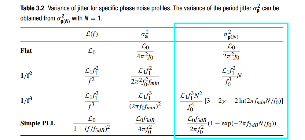
Flat: \(\mathcal{L}(f)=\mathcal{L}_0\)
statistically independent edges, the generator therefore perturbs each ideal edge directly, with no accumulation \[ t_n \;=\; nT_0 + a_n, \qquad a_n \stackrel{\text{iid}}{\sim} \mathcal{N}\!\left(0,\;\sigma_a^2\right), \qquad \sigma_a^2 = \frac{\mathcal{L}_0}{4\pi^2 f_0} \]
\(1/f^2\): \(\mathcal{L}(f)=\mathcal{L}_1 f_1^2/f^2\) (white FM)
\(\sigma_p^2(N)\;=\;\frac{\mathcal{L}_1 f_1^2}{f_0^3}\,N\) — Linear growth in \(N\) is the signature of independent increments, the generator injects an iid error into every period and accumulates edges: \[ t_n \;=\; t_{n-1} + T_0 + d_n, \qquad d_n \stackrel{\text{iid}}{\sim} \mathcal{N}\!\left(0,\;\sigma_\Delta^2\right), \qquad \sigma_\Delta^2 \;=\; \sigma_p^2(N{=}1) \;=\; \frac{\mathcal{L}_1 f_1^2}{f_0^3} \]
\(1/f^3\): \(\mathcal{L}(f)=\mathcal{L}_1 f_1^3/f^3\) (flicker FM)
shaping noise in the frequency domain
fftandifftare just tool to transform between time domain and frequency domain — we only care about input PSD (uniformly sampled discrete white noise) and final output PSD
1 | W = np.fft.rfft(rng.standard_normal(M)) |
This generates white Gaussian noise and transforms it to the frequency domain, i.e. Unit-variance sampled white noise has one-sided PSD \[ S_W = \frac{2}{f_s} \]
1 | H[1:] = 1.0 / np.sqrt(f[1:]) |
Filtering amplitudes by \(1/\sqrt f\) filters power by \[ |H(f)|^2=\frac{1}{f} \]
1 | return x * np.sqrt(c * fs / 2.0) |
Therefore, the resulting sequence has a \(1/f\) PSD. DC is set to zero because ideal \(1/f\) noise diverges at \(f=0\).
Unit-variance sampled white noise has one-sided PSD \(2/f_s\). Thus the output PSD is \[ S_o(f) = \frac{2}{f_s}\frac{1}{f} \left(\frac{c f_s}{2}\right) = \frac{c}{f} \]
1 | c_fl = 2 * L3 * f1 ** 3 / f0 ** 4 # 1/f^3: period-error PSD S_d(f)=c/f [s^2/Hz] |
\[ c_{fl} = \frac{2L_3f_1^3}{f_0^4} \]
1 | J["1_f3_only"] = np.cumsum(d3) |
Accumulation is discrete-time integration. Its exact transfer function is \[ |H_{\mathrm{acc}}(f)|^2 = \frac{1}{4\sin^2(\pi f/f_0)} \approx \frac{f_0^2}{4\pi^2f^2}, \qquad f\ll f_0 \] Consequently, the accumulated time-error PSD is
\[ S_J(f) \approx \frac{c}{f}\frac{f_0^2}{4\pi^2f^2} = \frac{c f_0^2}{4\pi^2f^3} \]
Timing error is converted to phase using \(\phi=2\pi f_0J\)
Therefore,
\[ S_\phi(f) =(2\pi f_0)^2S_J(f) \approx \frac{c f_0^4}{f^3} \] Since the code uses the usual phase-noise definition \(L(f)=S_\phi(f)/2\)
\[ L(f)=\frac{c f_0^4}{2f^3} \] The coefficient is selected as \(c_{fl} = \frac{2L_3f_1^3}{f_0^4}\). Substitution gives exactly the desired target:
\[ \boxed{L(f)=L_3\left(\frac{f_1}{f}\right)^3} \] In short:
\[ \underbrace{\frac1f}_{\text{flicker period noise}} \times \underbrace{\frac1{f^2}}_{\text{accumulation}} = \underbrace{\frac1{f^3}}_{\text{phase noise}} \]
1 | EULER_GAMMA = 0.5772156649015329 |
Let the input period error be (d[n]), and let the accumulated timing error be \(J[n]=J[n-1]+d[n]\)
This is exactly what np.cumsum(d) implements, assuming
\(J[-1]=0\)
Taking the (z)-transform: \(J(z)=z^{-1}J(z)+D(z)\)
Rearranging \(J(z)(1-z^{-1})=D(z)\)
so the accumulator transfer function is \[ H_{\mathrm{acc}}(z) =\frac{J(z)}{D(z)} =\frac{1}{1-z^{-1}} \]
To obtain its frequency response, evaluate it on the unit circle: \(z=e^{j\omega}\)
Therefore, \[ H_{\mathrm{acc}}(e^{j\omega}) = \frac{1}{1-e^{-j\omega}} \] Its power gain is the squared magnitude: \[ |H_{\mathrm{acc}}(e^{j\omega})|^2 = \frac{1}{|1-e^{-j\omega}|^2} \] The denominator can be simplified as
\[\begin{aligned} |1-e^{-j\omega}|^2 &=(1-e^{-j\omega})(1-e^{j\omega})\\ &=2-e^{j\omega}-e^{-j\omega}\\ &=2-2\cos\omega\\ &=4\sin^2\left(\frac{\omega}{2}\right) \end{aligned}\]
Thus the exact discrete-time power gain is
\[ \boxed{ |H_{\mathrm{acc}}(e^{j\omega})|^2 = \frac{1}{4\sin^2(\omega/2)} } \]
references
AN10007 Clock Jitter Definitions and Measurement Methods, SiTime [pdf]
SERDES Design and Simulation Using the Analog FastSPICE Platform, Silicon Creations [pdf]
Flexible clocking solutions in advanced processes from 180nm to 5nm, Silicon Creations [pdf]
One-size-fits-all PLLs for Advanced Samsung Foundry Processes, Silicon Creations [pdf]
Circuit Design and Verification of 7nm LowPower, Low-Jitter PLLs, Silicon Creations, [pdf]
Lecture 10: Jitter, ECEN720: High-Speed Links Circuits and Systems Spring 2023 [pdf]
Jitter 360° Knowledge Series [pdf, slides]
N. Da Dalt, "Tutorial: Jitter: Basic and Advanced Concepts, Statistics, and Applications," 2012 IEEE International Solid-State Circuits Conference, San Francisco, CA, USA, 2012 [slides, transcript ]