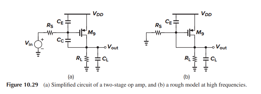
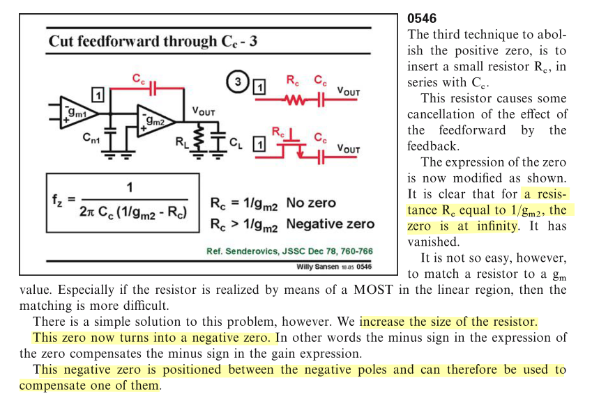
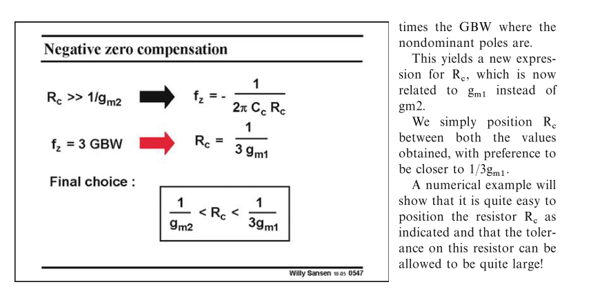
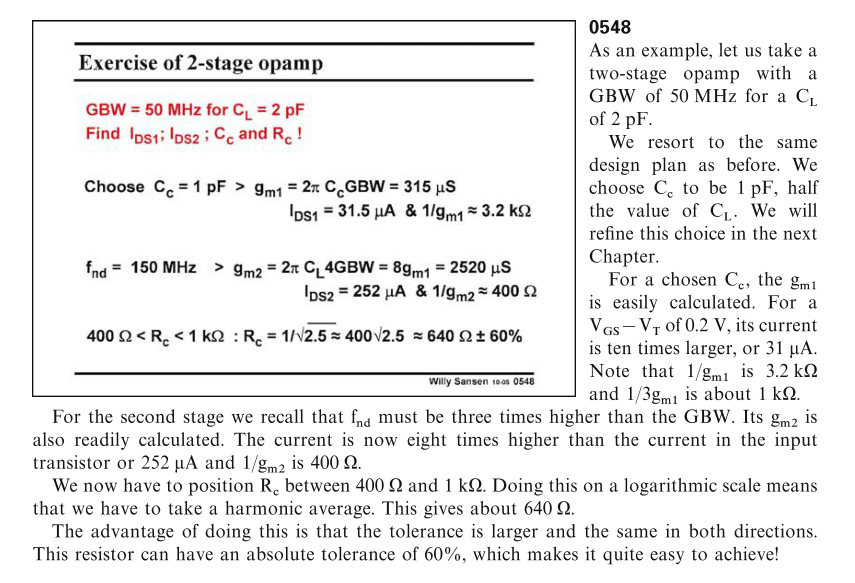
Frequency Compensation
Miller's approximation

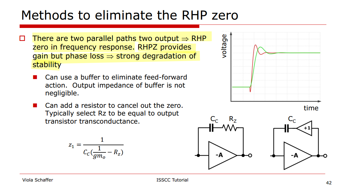
Right-Half-Plane Zero
\[ \left[(v_i - v_o)sC_c - g_m v_i\right]R_o = v_o \] Then \[ \frac{v_o}{v_i} = -g_mR_o\frac{1-s\frac{C_c}{g_m}}{1+sR_oC_c} \] right-half-plane Zero \(\omega _z = \frac{g_m}{C_c}\)
Equivalent cap
The amplifier gain magnitude \(A_v = g_m R_o\) \[ I_\text{c,in} = (v_i - v_o)sC_c \] Then \[\begin{align} I_\text{c,in} &= (v_i + A_v v_i)sC_c \\ & = v_i s (1+A_v)C_c \end{align}\]
we get \(C_\text{in,eq}= (1+A_v)C_c\simeq A_vC_c\)
Similarly \[\begin{align} I_\text{c,out} &= (v_o - v_i)sC_c \\ & = v_o s (1+\frac{1}{A_v})C_c \end{align}\]
we get \(C_\text{out,eq}= (1+\frac{1}{A_v})C_c\approx C_c\)
Pole Splitting
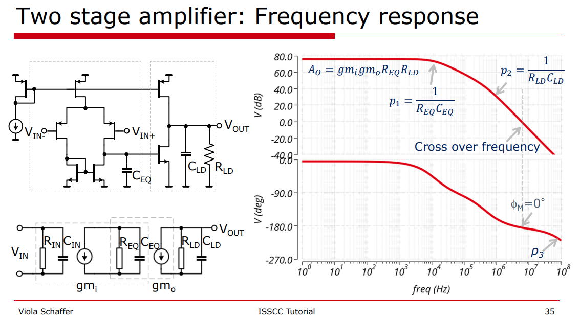
Generic circuit in textbook
In addition to lowering the required capacitor value, Miller compensation entails a very important property: it moves the output pole away from the origin. This effect is called pole splitting
The 1st stage is replaced with Thevenin equivalent circuit , \(V_i \approx V_i \cdot g_{m1}R_{o1}\)
\[\begin{align} \frac{V_i-V_{o1}}{R_{o1}} &= V_{o1}\cdot sC_{o1}+(V_{o1}-V_o)\cdot sC_c \\ V_{o1} &= \frac{V_i+sR_{o1}C_cV_o}{1+sR_{o1}(C_{o1}+C_c)} \end{align}\] \[ (V_{o1}-V_o)sC_c=g_{m2}V_{o1}+V_o(\frac{1}{R_{o2}+sC_L}) \] substitute \(V_{o1}\), we get
\[\begin{align} \frac{V_o}{V_i} &= \frac{(sC_c-g_{m2})R_{o2}}{s^2R_{o1}R_{o2}(C_cC_{o1}+C_LC_{o1}+C_LC_c)+s\left\{ R_{o1}C_c\cdot g_{m2}R_{o2}+R_{o2}(C_c+C_L)+R_{o1}(C_{o1}+C_c) \right\} +1} \\ &= \frac{g_{m2}R_{o2}(s\frac{C_c}{g_{m2}}-1)}{s^2R_{o1}R_{o2}(C_cC_{o1}+C_LC_{o1}+C_LC_c)+s\left\{ R_{o1}C_c\cdot g_{m2}R_{o2}+R_{o2}(C_c+C_L)+R_{o1}(C_{o1}+C_c) \right\} +1} \end{align}\]
left hand plane poles
\[\begin{align} \omega_1 &= \frac{1}{R_{o1}C_c\cdot g_{m2}R_{o2}+R_{o2}(C_c+C_L)+R_{o1}(C_{o1}+C_c)} \\ \omega_2 &= \frac{R_{o1}C_c\cdot g_{m2}R_{o2}+R_{o2}(C_c+C_L)+R_{o1}(C_{o1}+C_c)}{R_{o1}R_{o2}(C_cC_{o1}+C_LC_{o1}+C_LC_c)} \end{align}\]
and RHP (right-hand plane) zero \[ \omega_z=\frac{g_{m2}}{C_c} \]
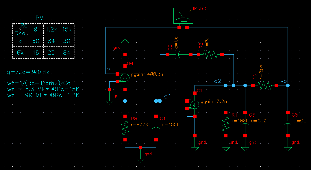
with series switch
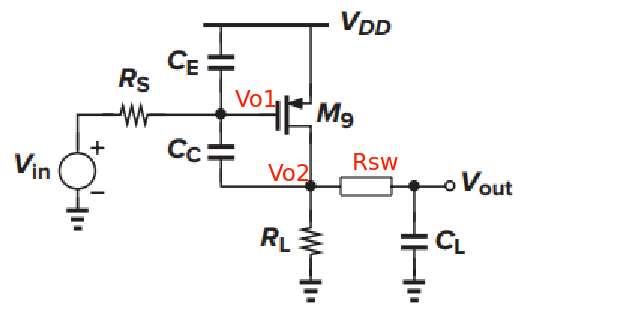
replace \(sC_L\) with \(1/(R_{sw}+\frac{1}{sC_L})\) \[\begin{align} \frac{V_{o2}}{V_i} &= \frac{g_{m2}R_{o2}(s\frac{C_c}{g_{m2}}-1)(1+sR_{sw}C_L)}{s^3R_{o1}R_{o2}R_{sw}C_{o1}C_cC_L+s^2\left\{R_{o1}R_{o2}(C_cC_{o1}+C_LC_{o1}+C_LC_c)+ \left[ R_{o1}C_c\cdot g_{m2}R_{o2}+R_{o2}(C_c+0)+R_{o1}(C_{o1}+C_c)\right]R_{sw}C_L \right\}+s\left\{ R_{o1}C_c\cdot g_{m2}R_{o2}+R_{o2}(C_c+C_L)+R_{o1}(C_{o1}+C_c) +R_{sw}C_L\right\} +1} \end{align}\] Due to \[ \frac{V_o}{V_{o2}} = \frac{\frac{1}{sC_L}}{R_{sw}+\frac{1}{sC_L}}=\frac{1}{1+sR_{sw}C_L} \] Then \[\begin{align} \frac{V_o}{V_i} &= \frac{V_{o2}}{V_i} \cdot \frac{V_o}{V_{o2}} \\ &= \frac{g_{m2}R_{o2}(s\frac{C_c}{g_{m2}}-1)}{s^3R_{o1}R_{o2}R_{sw}C_{o1}C_cC_L+s^2\left\{R_{o1}R_{o2}(C_cC_{o1}+C_LC_{o1}+C_LC_c)+ \left[ R_{o1}C_c\cdot g_{m2}R_{o2}+R_{o2}(C_c+0)+R_{o1}(C_{o1}+C_c)\right]R_{sw}C_L \right\}+s\left\{ R_{o1}C_c\cdot g_{m2}R_{o2}+R_{o2}(C_c+C_L)+R_{o1}(C_{o1}+C_c) +R_{sw}C_L\right\} +1} \end{align}\]
\(R_{sw}\) & \(R_c\)
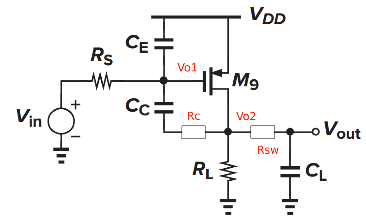
\[\begin{align} \frac{V_{o2}}{V_i} &=-g_{m2}R_{o2}\frac{sC_c(R_c-1/g_{m2})+1}{(1+sR_{o1}C_{o1})sR_{o2}C_c+sR_{o1}\cdot g_{m2}R_{o2}C_c+\frac{s(R_{o2}+R_{sw})C_L+1}{sR_{sw}C_L+1}\left[(1+sR_{o1}C_{o1})(1+sR_cC_c)+sR_{o1}C_c \right]} \\ &=-g_{m2}R_{o2}\frac{sC_c(R_c-1/g_{m2})+1}{s^2R_{o1}R_{o2}C_{o1}C_c+sR_{o2}C_c+sR_{o1}\cdot g_{m2}R_{o2}C_c+\frac{s(R_{o2}+R_{sw})C_L+1}{sR_{sw}C_L+1}\left[(1+sR_{o1}C_{o1})(1+sR_cC_c)+sR_{o1}C_c \right]} \\ &=-g_{m2}R_{o2}\frac{\left[ sC_c(R_c-1/g_{m2})+1 \right](sR_{sw}C_L+1)}{s^2R_{o1}R_{o2}C_{o1}C_c(sR_{sw}C_L+1)+sR_{o2}C_c(sR_{sw}C_L+1)+sR_{o1}\cdot g_{m2}R_{o2}C_c(sR_{sw}C_L+1)+\left[s(R_{o2}+R_{sw})C_L+1\right]\left[(1+sR_{o1}C_{o1})(1+sR_cC_c)+sR_{o1}C_c \right]} \end{align}\]
\(s^3\) terms in denominator \[ H_3 = s^3\cdot(R_{o1}R_{o2}R_c+R_{o1}R_{o2}R_{sw} +R_{o1}R_cR_{sw})\cdot C_{o1}C_cC_L \] \(s^2\) terms in denominator \[\begin{align} H_2 &=s^2\cdot(R_{o1}R_{o2}C_{o1}C_c+R_{o1}R_{o2}C_{o1}C_L+R_{o2}R_cC_cC_L+R_{o1}R_{o2}C_cC_L+R_{o1}R_cC_{o1}C_c\\ &+R_{o2}R_{sw}C_cC_L+R_{o1}R_{sw}C_cC_L\cdot g_{m2}R_{o2}+R_{o1}R_{sw}C_{o1}C_L+R_{sw}R_cC_cC_L+R_{o1}R_{sw}C_cC_L) \end{align}\]
\(s^1\) term in denominator \[ H_1=s(R_{o1}\cdot g_{m2}R_{o2}C_c+R_{o1}C_{o1}+R_cC_c+R_{o1}C_c+R_{o2}C_c+R_{o2}C_L+R_{sw}C_L) \] \(s^0\) term in denominator \[ H_0=1 \] set \(R_c=0\) and \(R_{sw}=0\), the \(H_*\) reduced to \[\begin{align} H_3 &= 0 \\ H_2 &=s^2R_{o1}R_{o2}(C_{o1}C_c+C_{o1}C_L+C_cC_L) \\ H_1&=s(R_{o1}\cdot g_{m2}R_{o2}C_c+R_{o1}C_{o1}+R_{o1}C_c+R_{o2}C_c+R_{o2}C_L) \\ H_0&=1 \end{align}\] That is \[ H=s^2R_{o1}R_{o2}(C_{o1}C_c+C_{o1}C_L+C_cC_L)+s(R_{o1}\cdot g_{m2}R_{o2}C_c+R_{o1}C_{o1}+R_{o1}C_c+R_{o2}C_c+R_{o2}C_L)+1 \]
which is same with our previous analysis of Generic circuit in textbook
And we know \[ \frac{V_o}{V_{o2}}=\frac{1}{1+sR_{sw}C_L} \] Finally, we get \(\frac{V_o}{V_i}\) \[\begin{align} \frac{V_o}{V_i} &= \frac{V_{o2}}{V_i} \cdot \frac{V_o}{V_{o2}} \\ &= -g_{m2}R_{o2}\frac{\left[ sC_c(R_c-1/g_{m2})+1 \right](sR_{sw}C_L+1)}{H_3+H_2+H_1+1} \cdot \frac{1}{1+sR_{sw}C_L} \\ &= -g_{m2}R_{o2}\frac{ sC_c(R_c-1/g_{m2})+1}{H_3+H_2+H_1+1} \end{align}\]
The loop transfer function is \[ \frac{V_o}{V_i} =-g_{m1}R_{o1}g_{m2}R_{o2}\frac{ sC_c(R_c-1/g_{m2})+1}{H_3+H_2+H_1+1} \]
vccs model
simplify the transfer function
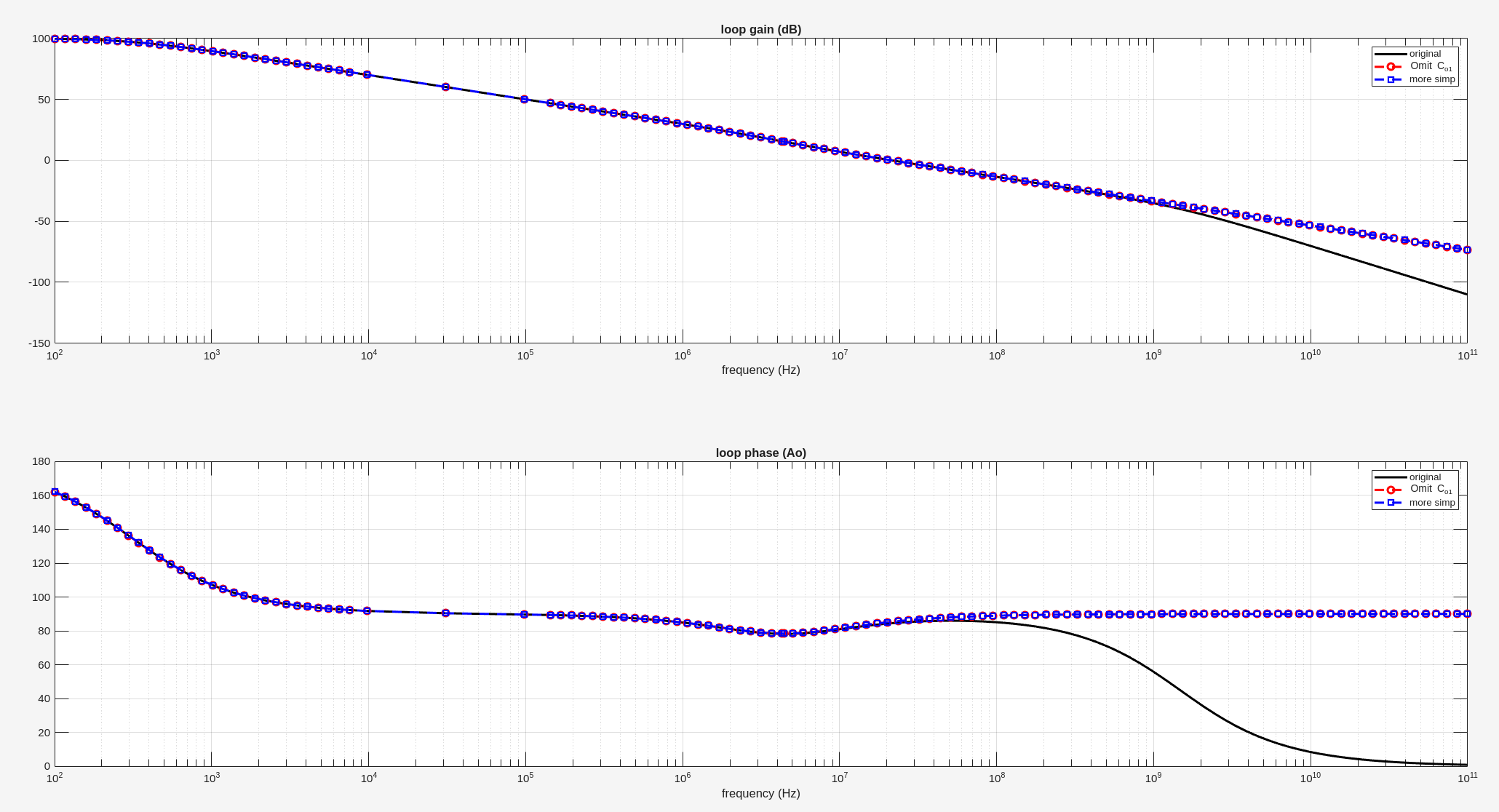
- omit \(C_{o1}\)
We omit \(C_{o1}\) in frequency range of interest
\[\begin{align} H_3 &= 0 \\ H_2 &=s^2(R_{o2}R_c+R_{o1}R_{o2}+R_{o2}R_{sw}+R_{o1}R_{sw}\cdot g_{m2}R_{o2}+R_{sw}R_c+R_{o1}R_{sw})\cdot C_cC_L \\ H_1 &=s(R_{o1}\cdot g_{m2}R_{o2}C_c+R_cC_c+R_{o1}C_c+R_{o2}C_c+R_{o2}C_L+R_{sw}C_L) \\ H_0 &= 1 \end{align}\]
two poles and 1 zero
- more simplification
Then, some terms can be omitted
\[\begin{align} H_2 &=s^2R_{o1}R_{o2}(1+g_{m2}R_{sw})\cdot C_cC_L \\ H_1 &=sR_{o1}\cdot g_{m2}R_{o2}C_c \\ H_0 &= 1 \end{align}\]
The poles can be deduced \[\begin{align} \omega_1 &= \frac{1}{R_{o1}\cdot g_{m2}R_{o2}C_c} \\ \omega_2 &= \frac{1}{1+g_{m2}R_{sw}}\cdot \frac{g_{m2}}{C_L} \\ &= \frac{1}{(g_{m2}^{-1}+R_{sw})C_L} \end{align}\]
The pole \(\omega_2=\frac{1}{g_{m2}^{-1}C_L}\) is changed to \(\omega_2=\frac{1}{(g_{m2}^{-1}+R_{sw})C_L}\)
In order to cancel \(\omega_2\) with \(\omega_z\), \(R_c\) shall be increased
\[ R_{eq}=g_{m2}^{-1}+R_{sw} \]

1 | gm1 = 400e-6; |
non-dominant pole in Sansen's book
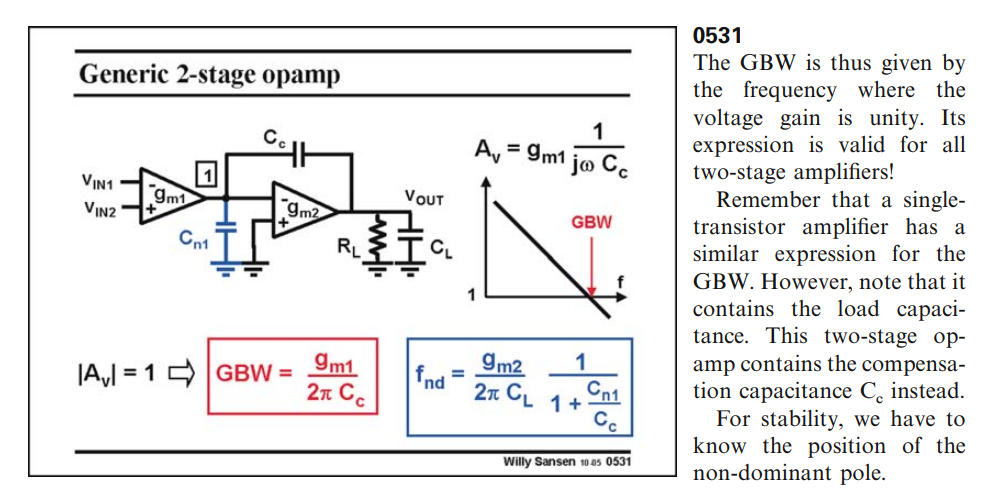
Following demonstrate how derive \(f_{nd}\) from Razavi's equation. We copy \(\omega_2\) here \[ \omega_2 = \frac{R_{o1}C_c\cdot g_{m2}R_{o2}+R_{o2}(C_c+C_L)+R_{o1}(C_{o1}+C_c)}{R_{o1}R_{o2}(C_cC_{o1}+C_LC_{o1}+C_LC_c)} \] which can be reduced as below
\[\begin{align} \omega_2 &= \frac{R_{o1}C_c\cdot g_{m2}R_{o2}+R_{o2}(C_c+C_L)+R_{o1}(C_{o1}+C_c)}{R_{o1}R_{o2}(C_cC_{o1}+C_LC_{o1}+C_LC_c)} \\ &= \frac{R_{o1}C_c\cdot g_{m2}R_{o2}}{R_{o1}R_{o2}(C_cC_{o1}+C_LC_{o1}+C_LC_c)} = \frac{C_c\cdot g_{m2}}{C_cC_{o1}+C_LC_{o1}+C_LC_c} \\ &= \frac{g_{m2}}{C_{o1}+C_L\frac{C_{o1}}{C_c}+C_L} = \frac{g_{m2}}{C_L\frac{C_{o1}}{C_c}+C_L} = \frac{g_{m2}}{C_L} \cdot \frac{1}{1+\frac{C_{o1}}{C_c}} \end{align}\]
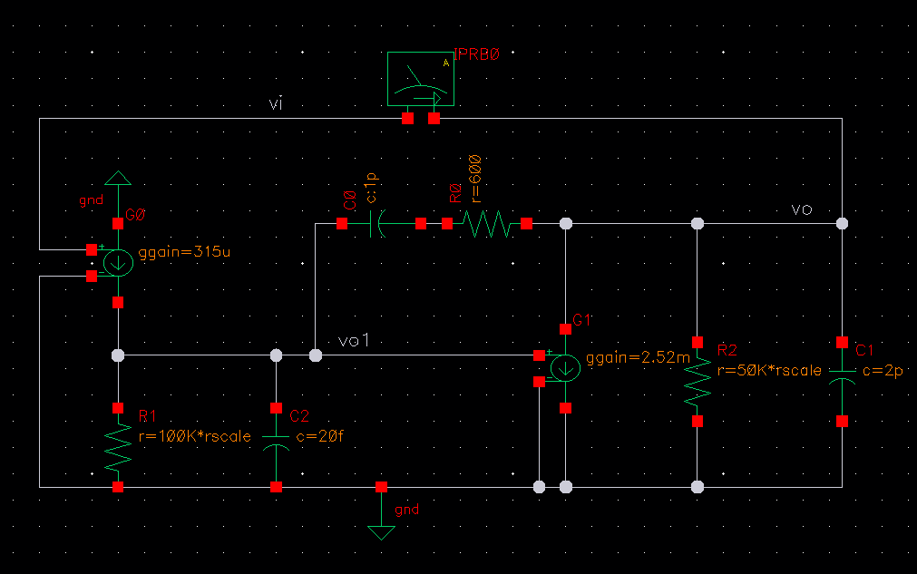
Exercise of 2-stage opamp
\(R_{o1}\) and \(R_{o2}\) don't affect stability, if \(f_{nd}>3\text{GBW}\)
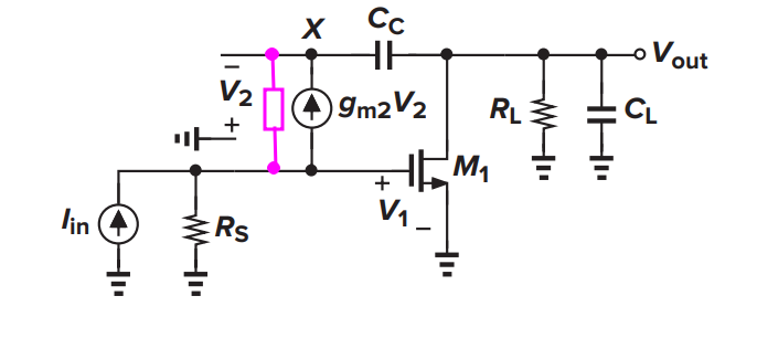
DC gain: \(g_{m1}g_{m2}R_{o1}R_{o2}\)
dominant pole: \(\omega_d=\frac{1}{R_{o1}\cdot g_{m2}R_{o2}C_c}\)
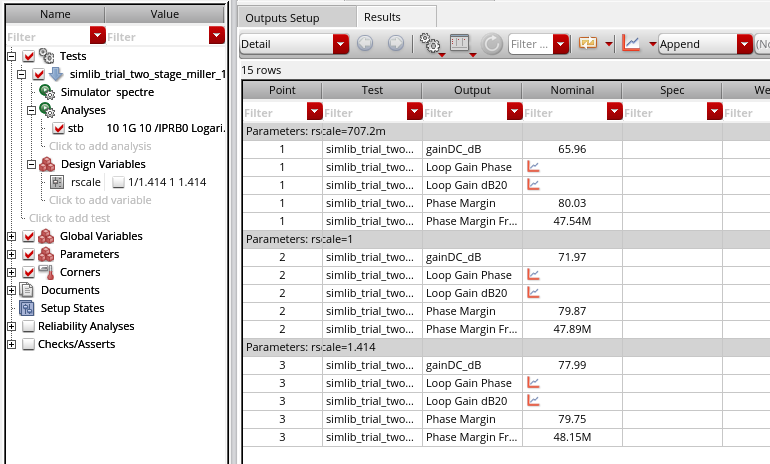
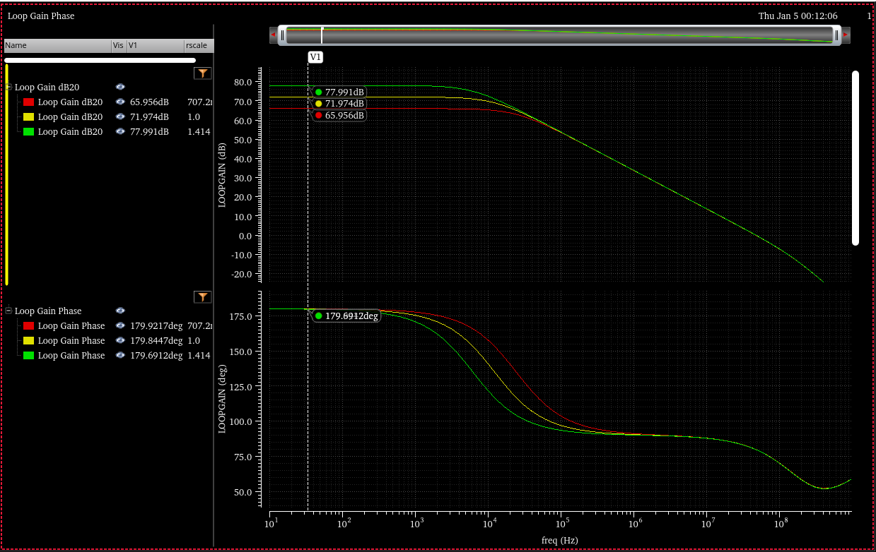
\(20log_{10}(1.414^2)=6\text{dB}\)
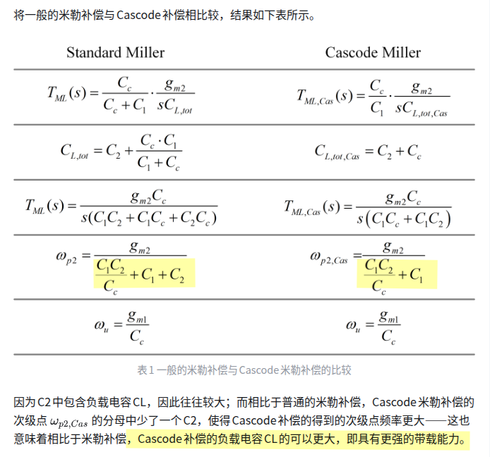
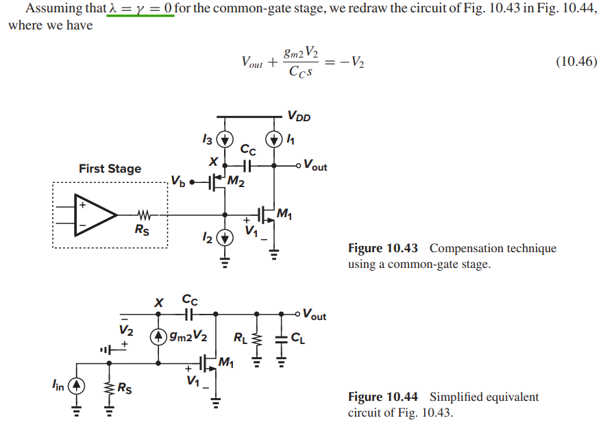
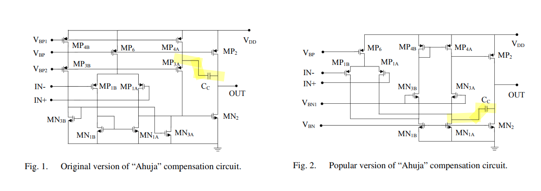
Ahuja Compensation
This Ahuja compensation topology is popularly known as cascode compensation
The cause of the positive zero is the feedforward current through \(C_m\).
To abolish this zero, we have to cut the feedforward path and create a unidirectional feedback through \(C_m\).
Adding a resistor(nulling resistor) is one way to mitigate the effect of the feedforward current.
Another approach uses a current buffer cascode to pass the small-signal feedback current but cut the feedforward current
[https://people.eecs.berkeley.edu/~boser/courses/240B/lectures/M07%20OTA%20II.pdf]
王小桃带你读文献. Cascode补偿前传—Ahuja补偿 Ahuja Compensation [https://zhuanlan.zhihu.com/p/1904126782900245880]
—. 两级运放的米勒补偿与Cascode米勒补偿 [https://zhuanlan.zhihu.com/p/10217022358]
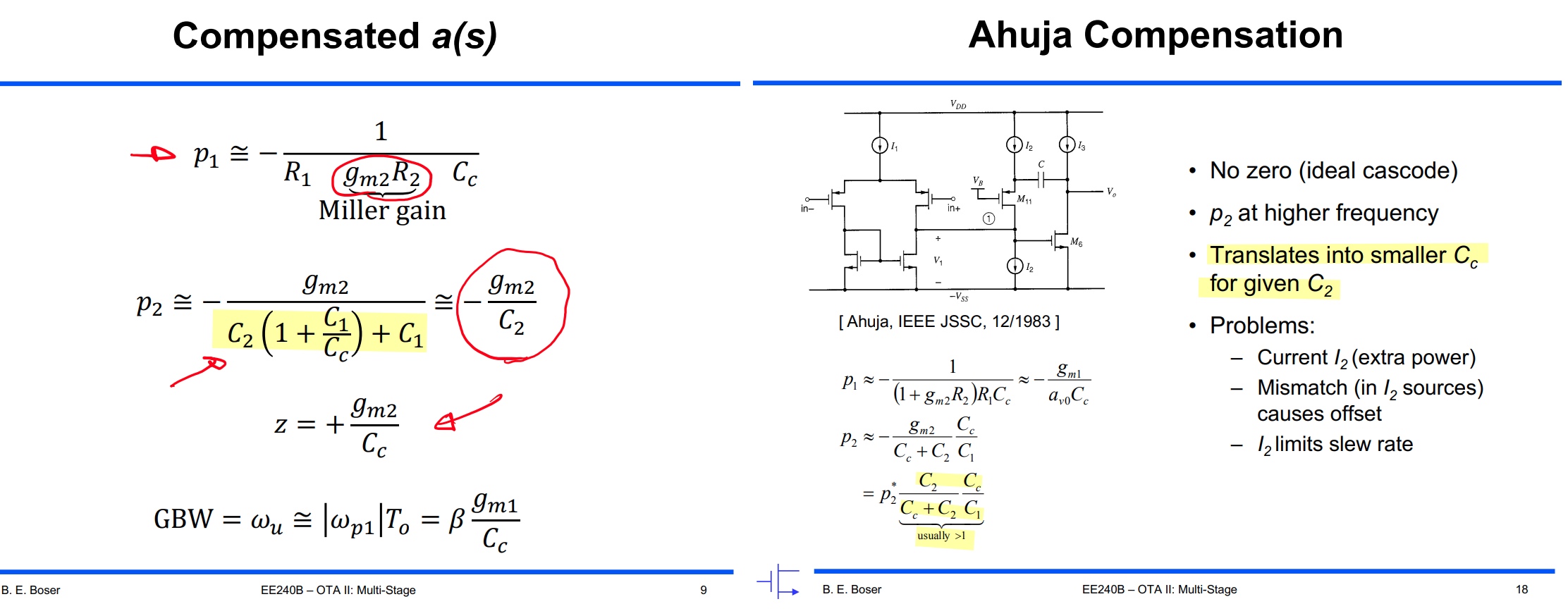
The benefits of Ahuja compensation over Miller compensation are severa
better PSRR
higher unity-gain bandwidth using smaller compensation capacitor
ability to cope better with heavy capacitive and resistive loads
Of course, , if the capacitance at the gate of \(M_1\) is taken into account, pole splitting is less pronounced.
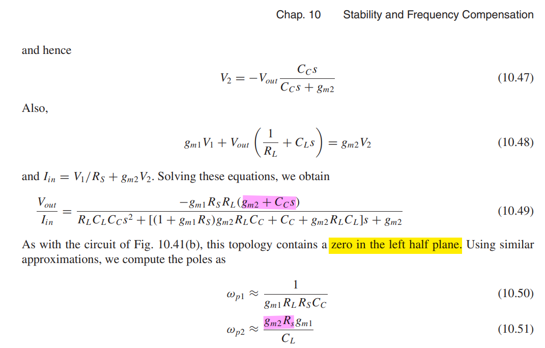
including \(r_\text{o2}\)
 \[
\frac{V_{out}}{I_{in}} \approx
\frac{-g_{m1}R_SR_L(g_{m2}+C_Cs)}{\frac{R_S+r_\text{o2}}{r_\text{o2}}R_LC_LC_Cs^2+g_{m1}g_{m2}R_LR_SC_Cs+g_{m2}}
\] The poles as
\[
\frac{V_{out}}{I_{in}} \approx
\frac{-g_{m1}R_SR_L(g_{m2}+C_Cs)}{\frac{R_S+r_\text{o2}}{r_\text{o2}}R_LC_LC_Cs^2+g_{m1}g_{m2}R_LR_SC_Cs+g_{m2}}
\] The poles as
\[\begin{align} \omega_{p1} &\approx \frac{1}{g_{m1}R_LR_SC_c} \\ \omega_{p2} &\approx \frac{g_{m2}R_Sg_{m1}}{C_L}\frac{r_\text{o2}}{R_S+r_\text{o2}} \end{align}\]
and zero is not affected, which is \(\omega_z =\frac{g_{m2}}{C_C}\)
the above model simulation result is shown below
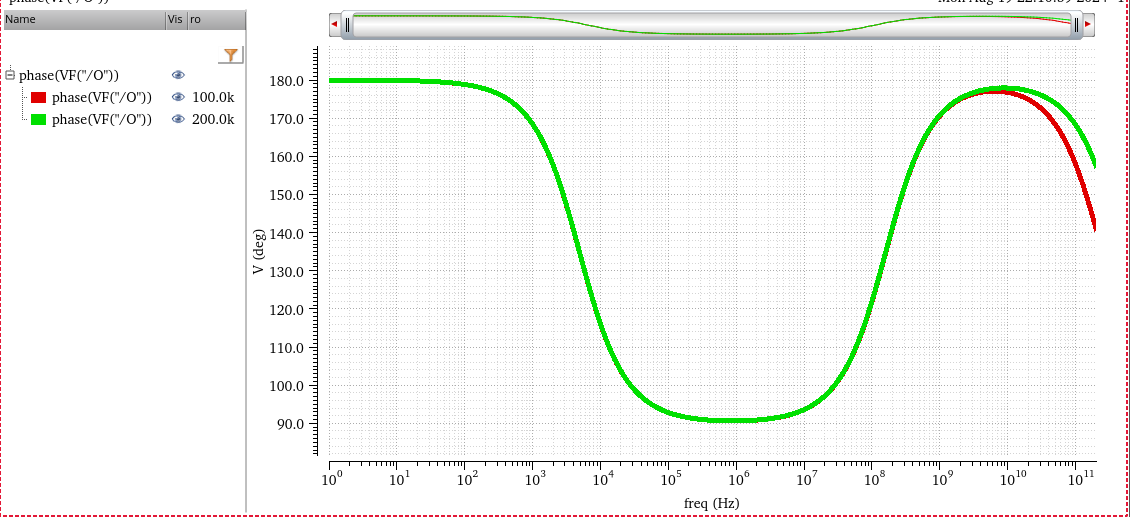
the zero is located between two poles
take into the capacitance at the gate of \(M_1\) and all other second-order effect
intuitive analysis of zero
miller compensation
- zero in the right half plane \[ g_\text{m1}V_P = sC_c V_P \]
cascode compensation
- zero in the left half plane \[ g_\text{m2}V_X = - sC_c V_X \]

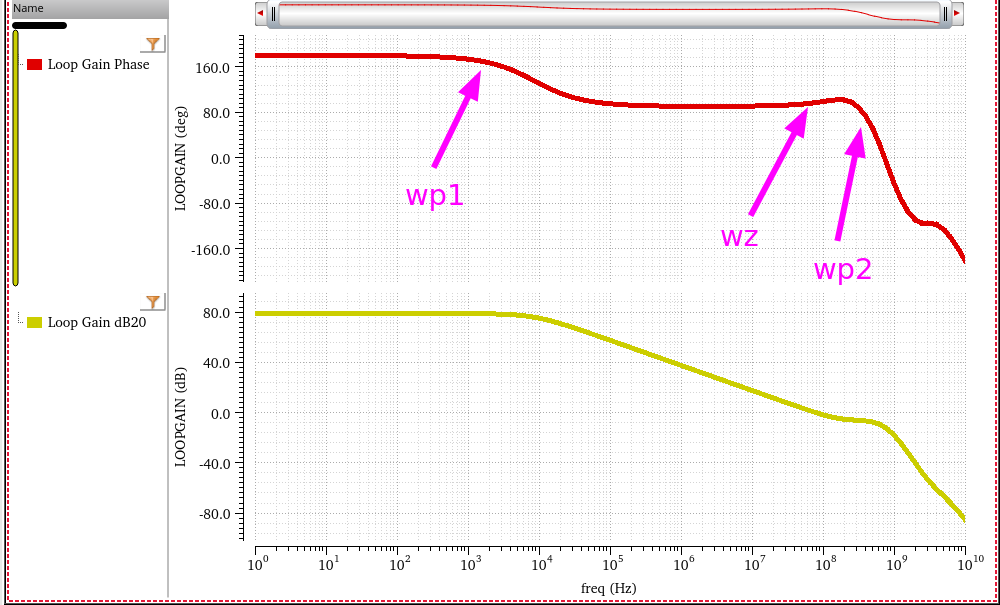
Mitigate Impact of Zero
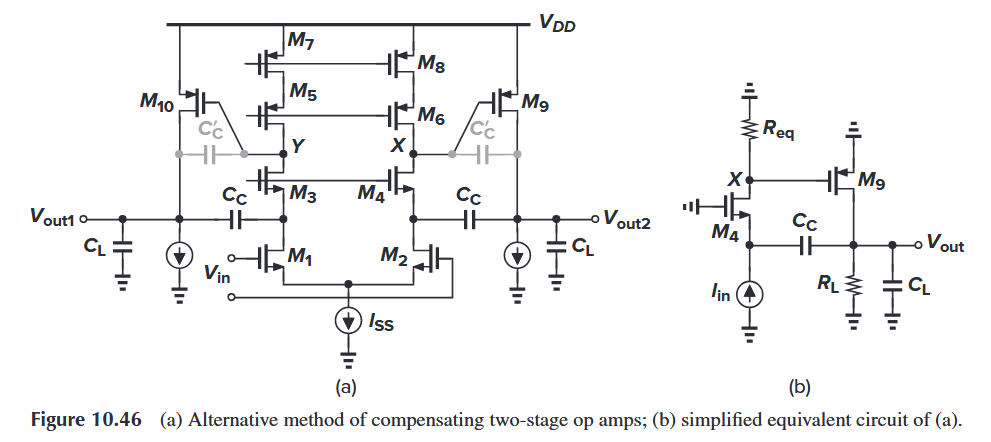
dominant pole \[ \omega_\text{p,d} = \frac {1} {R_\text{eq}g_\text{m9}R_{L}C_{c}} \] first nondominant pole \[ \omega_\text{p,nd} = \frac {g_\text{m4}R_\text{eq}g_\text{m9}} {C_L} \] zero \[ \omega_\text{z} = (g_\text{m4}R_\text{eq})(\frac {g_\text{m9}} {C_c}) \] a much greater magnitude than \(g_\text{m9}/C_C\)
ahuja variations
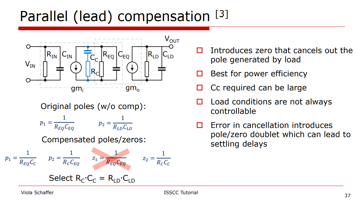
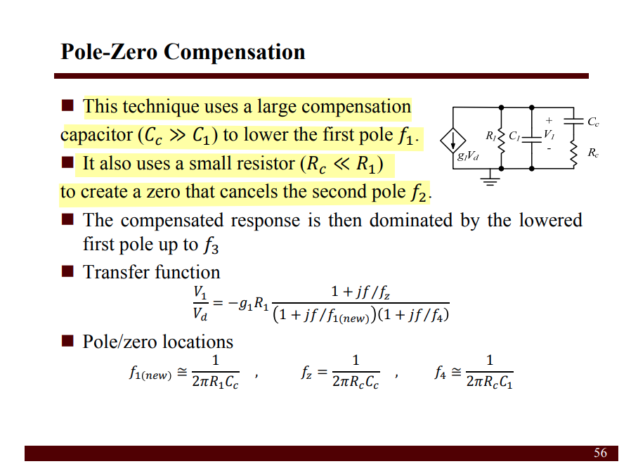
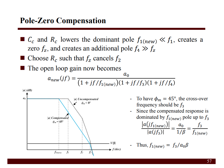
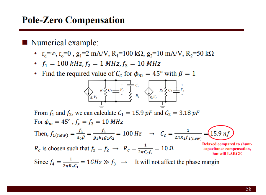
Pole-Zero Compensation
Pole-Zero Compensation is also known as Lead Compensation, Parallel Compensation
Note: The dominant pole is at output of the first stage, i.e. \(\frac{1}{R_{EQ}C_{EQ}}\).
Pole & Zero in transfer function
Design with operational amplifiers and analog integrated circuits / Sergio Franco, San Francisco State University. – Fourth edition
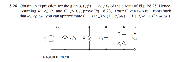
\[ Y = \frac{1}{R_1} + sC_1+\frac{1}{R_c+1/SC_c} \]
\[\begin{align} Z &= \frac{1}{\frac{1}{R_1} + sC_1+\frac{1}{R_c+1/SC_c}} \\ &= \frac{R_1(1+sR_cC_c)}{s^2R_1C_1R_cC_c+s(R_1C_c+R_1C_1+R_cC_c)+1} \end{align}\] If \(p_{1c} \ll p_{3c}\), two real roots can be found \[\begin{align} p_{1c} &= \frac{1}{R_1C_c+R_1C_1+R_cC_c} \\ p_{3c} &= \frac{R_1C_c+R_1C_1+R_cC_c}{R_1C_1R_cC_c} \end{align}\]
The additional zero is \[ z_c = \frac{1}{R_cC_c} \] Given \(R_c \ll R\) and \(C_c \gg C\) \[\begin{align} p_{1c} &\simeq \frac{1}{R_1(C_c+C_1)} \simeq \frac{1}{R_1C_c}\\ p_{3c} &= \frac{1}{R_cC_1}+\frac{1}{R_cC_c}+\frac{1}{R_1C_1} \simeq \frac{1}{R_cC_1} \end{align}\]
The output pole is unchanged, which is \[ p_2 = \frac{1}{R_LC_L} \] We usually cancel \(p_2\) with \(z_c\), i.e. \[ R_cC_c=R_LC_L \]
Phase margin
unity-gain frequency \(\omega_t\) \[ \omega_t = A_\text{DC}\cdot P_{1c} =\frac{g_{m1}g_{m2}R_L}{C_c} \]
PM=45\(^o\) \[ p_{3c} = \omega_t \] Then, \(C_c\) and \(R_c\) can be obtained
\[\begin{align} R_c &= \sqrt{\frac{R_1}{C_1\cdot A_{DC}\cdot p_2}}=\sqrt{\frac{R_1\cdot R_LC_L}{C_1\cdot A_{DC}}} \\ C_c &= \sqrt{\frac{A_{DC}\cdot C_1}{R_1\cdot p_2}}=\sqrt{\frac{A_{DC}\cdot C_1 \cdot R_LC_L}{R_1}} \end{align}\]
PM=60\(^o\) \[ p_{3c} = 2\cdot\omega_t \] Then, \(C_c\) and \(R_c\) can be obtained \[\begin{align} R_c &= \sqrt{\frac{R_1}{C_1\cdot 2A_{DC}\cdot p_2}} = \sqrt{\frac{R_1\cdot R_LC_L}{C_1\cdot 2A_{DC}}} \\ &= \sqrt{\frac{C_L}{2g_{m1}g_{m2}C_1}}\\ C_c &= \sqrt{\frac{2A_{DC}\cdot C_1}{R_1\cdot p_2}} = \sqrt{\frac{2A_{DC}\cdot C_1 \cdot R_LC_L}{R_1}} \\ &= R_L\sqrt{2g_{m1}g_{m2}C_1C_L} \end{align}\]
for the unity-gain frequency \(\omega_t\) we find \[ \omega_t = \sqrt{\frac{1}{2}\cdot \frac{g_{m1}g_{m2}}{C_1C_L}} \] The parallel compensation shows a remarkably good result. The new 0 dB frequency lies only a factor \(\sqrt{2}\) lower than the theoretical maximum
To increase \(\phi_m\), we need to raise \(C_c\) a bit while lowering \(R_c\) in proportion in order to maintain pole-zero cancellation. This causes \(p_{1c}\) and \(p_{3c}\) to split a bit further apart.
1 | clc; |
ECEN 457 (ESS). Op-Amps Stability and Frequency Compensation Techniques [https://people.engr.tamu.edu/s-sanchez/457%20Stability%20Final.pdf]
Pole-Zero Doublet
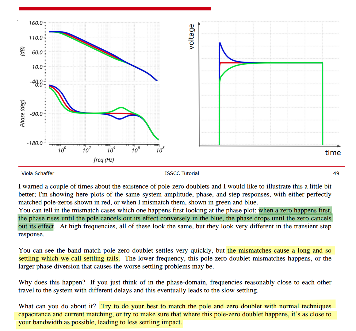
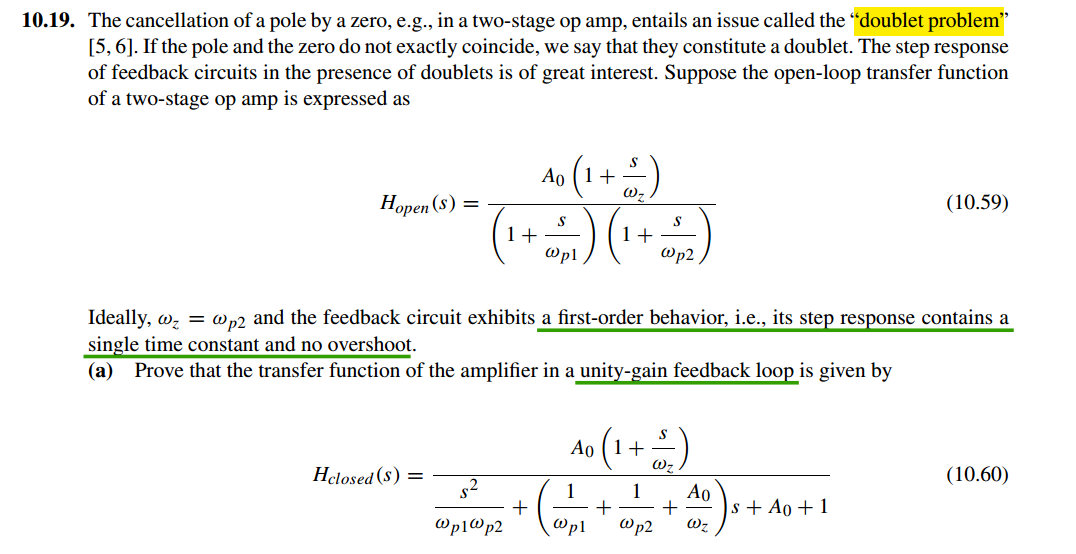
The denominator part of \(H_{closed}(s)\) is \[ D(s) = \frac{s^2}{(A_0+1)\omega_{p1}\omega_{p2}}+\frac{\frac{1}{\omega_{p1}} + \frac{1}{\omega_{p2}}+\frac{A_0}{\omega_{z}}}{A_0+1}s+1 \]
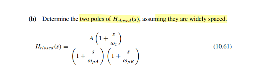
suppose \(\omega_{pA} \ll\omega_{pB}\), then \[ D(s) = \left( 1+ \frac{s}{\omega_{pA}}\right)\left( 1+ \frac{s}{\omega_{pB}}\right)\approx \frac{s^2}{\omega_{pA}\omega_{pB}}+\frac{s}{\omega_{pA}} + 1 \]
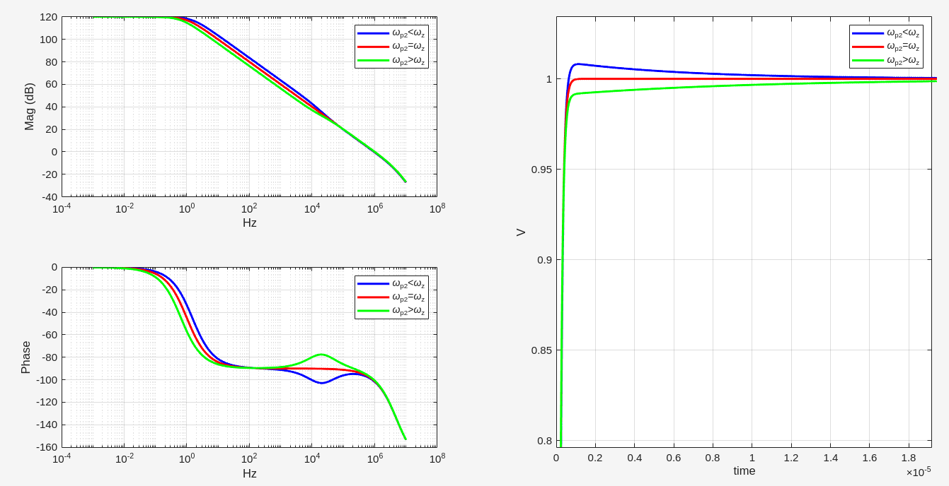
Thus, the two poles of the closed-loop transfer function of system are \[\begin{align} \omega_{pA} &= \frac{A_0+1}{\frac{1}{\omega_{p1}} + \frac{1}{\omega_{p2}}+\frac{A_0}{\omega_{z}}} = \frac{(A_0+1)\omega_{p1} \omega_{p2}}{\omega_{p1} + \omega_{p2} + \frac{A_0}{\omega_z}\omega_{p1} \omega_{p2}}\\ \omega_{pB} &= \omega_{p1} + \omega_{p2} + \frac{A_0}{\omega_z}\omega_{p1} \omega_{p2} \end{align}\]
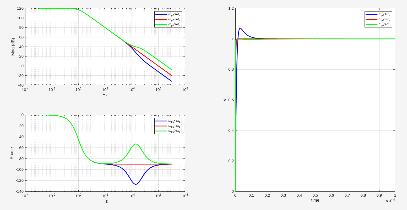
non-dominant pole \(\omega_{p2}\) and zero \(\omega_z\) are in UGB
\[\begin{align} \omega_{pA} &\approx \omega_{p2}\\ \omega_{pB} &\approx (1+A_0)\omega_{p1} \end{align}\] Then, closed-loop transfer function is \[ H_{closed}(s) \approx \frac{\frac{A_0}{A_0+1}\left(1+\frac{s}{\omega_z}\right)}{\left(1+\frac{s}{(1+A_0)\omega_{p1}}\right)\left( 1+\frac{s}{\omega_{p2}} \right)} \]
Consider the Laplace transform function of step response, \(X(s)=\frac{1}{s}\) \[
Y(s)=\frac{1}{s}\times H_{closed}(s)
\] Thus, the small-signal step response of the
closed-loop amplifier is \[
y(t)=\frac{A_0}{A_0+1}\left[1-e^{-(A_0+1)\omega_{p1}t}-\left(1-\frac{\omega_{p2}}{\omega_z}\right)e^{-\omega_{p2}t}
\right]u(t)
\] Since, \(\omega_{p2}\ll
(1+A_0)\omega_{p1}\). rewrite the \(y(t)\) \[
y(t)\approx
\frac{A_0}{A_0+1}\left[1-\left(1-\frac{\omega_{p2}}{\omega_z}\right)e^{-\omega_{p2}t}
\right]u(t)
\] 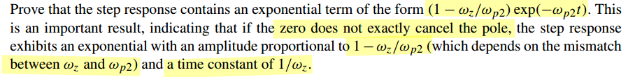
perfect pole-zero cancellation with \(\omega_{p2}=\omega_z\) \[ y(t) \approx \frac{A_0}{A_0+1}\left[1-e^{-(A_0+1)\omega_{p1}t}\right]u(t) \approx \frac{A_0}{A_0+1}u(t) \]
1 | clear |
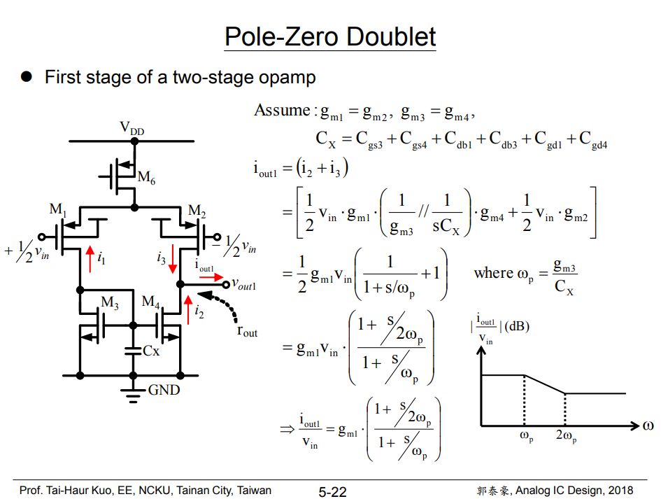
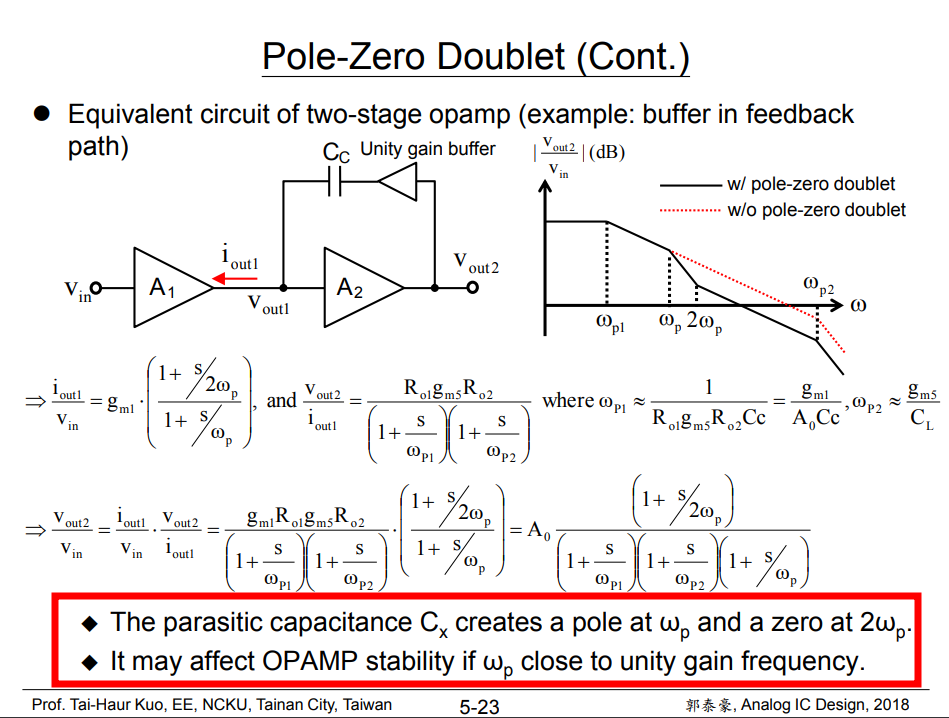
The zero comes from the mirror node
Thanks to unity gain buffer, zero is alleviated for \(C_c\)
1 | A0 = 1e6; |
reference
Viola Schaffer, ISSCC 2021 Tutorials Designing Amplifiers for Stability [pdf]
J. H. Huijsing, "Operational Amplifiers, Theory and Design, 3rd ed. New York: Springer, 2017"
Razavi, Behzad. Design of Analog CMOS Integrated Circuits. India: McGraw-Hill, 2017. [pdf]
Sansen, Willy M. Analog Design Essentials. Germany: Springer US, 2006.
Gray, P. R., Hurst, P. J., Lewis, S. H., & Meyer, R. G. (2024). Analysis and design of analog integrated circuits (Sixth edition.). John Wiley & Sons, Inc..
Ahuja Compensation
B. K. Ahuja, "An Improved Frequency Compensation Technique for CMOS Operational Amplifiers," IEEE 1. Solid-State Circuits, vol. 18, no. 6, pp. 629-633, Dec. 1983. [https://sci-hub.se/10.1109/JSSC.1983.1052012]
U. Dasgupta, "Issues in "Ahuja" frequency compensation technique", IEEE International Symposium on Radio-Frequency Integration Technology, 2009. [https://sci-hub.se/10.1109/RFIT.2009.5383679]
R. J. Reay and G. T. A. Kovacs, "An unconditionally stable two-stage CMOS amplifier," in IEEE Journal of Solid-State Circuits, vol. 30, no. 5, pp. 591-594, May 1995 [https://sci-hub.se/10.1109/4.384174]
A. Garimella and P. M. Furth, "Frequency compensation techniques for op-amps and LDOs: A tutorial overview," 2011 IEEE 54th International Midwest Symposium on Circuits and Systems (MWSCAS), 2011 [https://sci-hub.se/10.1109/MWSCAS.2011.6026315]
H. Aminzadeh, R. Lotfi and S. Rahimian, "Design Guidelines for Two-Stage Cascode-Compensated Operational Amplifiers," 2006 13th IEEE International Conference on Electronics, Circuits and Systems, 2006 [https://sci-hub.se/10.1109/ICECS.2006.379776]
H. Aminzadeh and K. Mafinezhad, "On the power efficiency of cascode compensation over Miller compensation in two-stage operational amplifiers," Proceeding of the 13th international symposium on Low power electronics and design (ISLPED '08), Bangalore, India, 2008 [https://sci-hub.se/10.1145/1393921.1393995]
Stabilizing a 2-Stage Amplifier URL:https://a2d2ic.wordpress.com/2016/11/10/stabilizing-a-2-stage-amplifier/
EE 240B: Advanced Analog Circuit Design, Prof. Bernhard E. Boser [OTA II, Multi-Stage]
Parallel Compensation
R.Eschauzier "Wide Bandwidth Low Power Operational Amplifiers", Delft University Press, 1994.
Gene F. Franklin, J. David Powell, and Abbas Emami-Naeini. 2018. Feedback Control of Dynamic Systems (8th Edition) (8th. ed.). Pearson. 6.7 Compensation
Application Note AN-1286 Compensation for the LM3478 Boost Controller
ECEN 607 Advanced Analog Circuit Design Techniques Spring 2017 [Lect 1D Op-Amps Stability and Frequency Compensation Techniques]
Sergio Franco, San Francisco State University, Design with Operational Amplifiers and Analog Integrated Circuits, 4/e [pdf]
Pole-Zero Doublet
Elad Alon, Lecture 10: Settling-Limited Amplifier Design Methodology, EE 240B – Spring 2018, Advanced Analog Integrated Circuits [https://inst.eecs.berkeley.edu/~ee240b/sp18/lectures/Lecture10_Settling_Design_2up.pdf]
Eric Chang, Prof. Elad Alon EE240B HW3 [https://inst.eecs.berkeley.edu/~ee240b/sp18/homeworks/hw3.pdf and https://inst.eecs.berkeley.edu/~ee240b/sp18/homeworks/hw3_soln.pdf]
Prof. Tai-Haur Kuo, Analog IC Design ( 類比積體電路設計 ), Operational Amplifiers http://msic.ee.ncku.edu.tw/course/aic/201809/chapter5.pdf
SERGIO FRANCO, Demystifying pole-zero doublets [https://www.edn.com/demystifying-pole-zero-doublets/]
B. Y. T. Kamath, R. G. Meyer and P. R. Gray, "Relationship between frequency response and settling time of operational amplifiers," in IEEE Journal of Solid-State Circuits, vol. 9, no. 6, pp. 347-352, Dec. 1974, [https://sci-hub.se/10.1109/JSSC.1974.1050527]
P. R. Gray and R. G. Meyer, "MOS operational amplifier design-a tutorial overview," in IEEE Journal of Solid-State Circuits, vol. 17, no. 6, pp. 969-982, Dec. 1982, [https://sci-hub.se/10.1109/JSSC.1982.1051851]