Clocking Miscellaneous
PD & PFD
Sam Palermo, ECEN620: Network Theory Broadband Circuit Design Fall 2025 Lecture 4: Phase Detector Circuits [https://people.engr.tamu.edu/spalermo/ecen620/lecture04_ee620_phase_detectors.pdf]
Michael Perrott, 6.976 High Speed Communication Circuits and Systems Lecture 15 Integer-N Frequency Synthesizers [https://rfic.eecs.berkeley.edu/courses/ee242/pdf/perrott_lec15.pdf]
Mehmet Soyuer. Monolithic Phase-Locked Loops for Clocking [https://ewh.ieee.org/r5/denver/sscs/Presentations/2009_06_Soyuer.pdf]
Qasim Chaudhari. What are Cycle Slips and Hangup in Phase Locked Loops? [https://wirelesspi.com/what-are-cycle-slips-and-hangup-in-phase-locked-loops/]
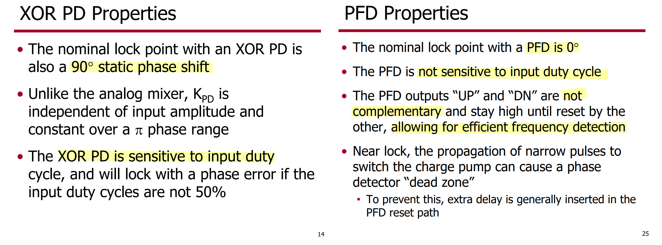
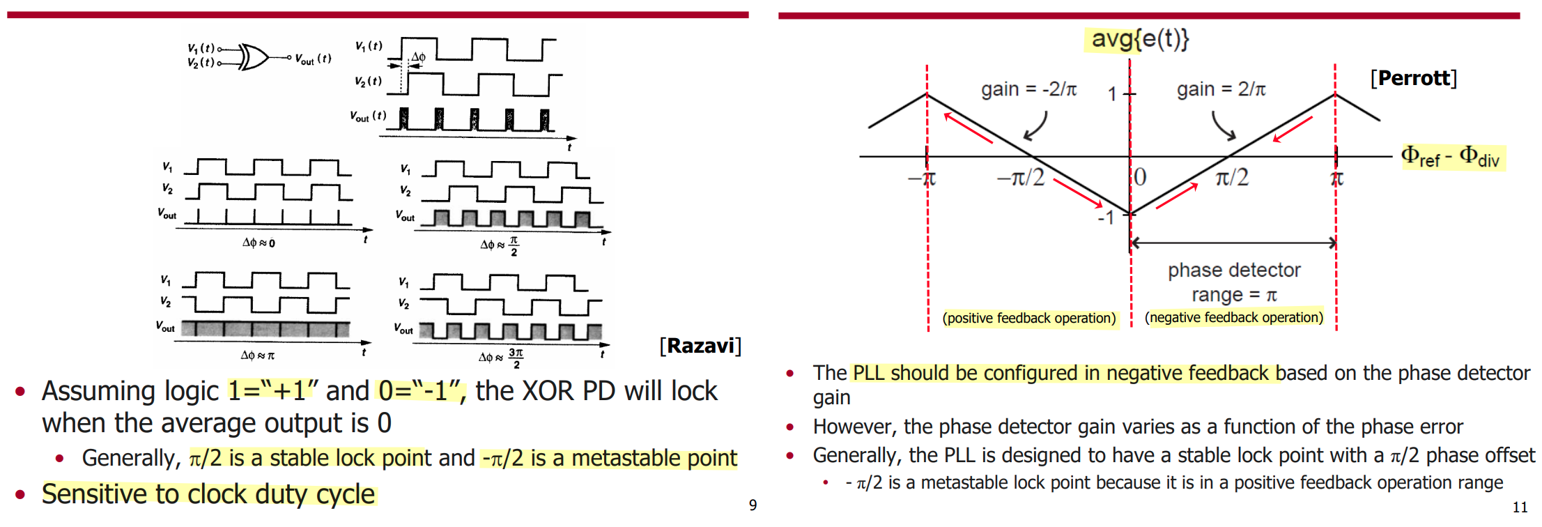
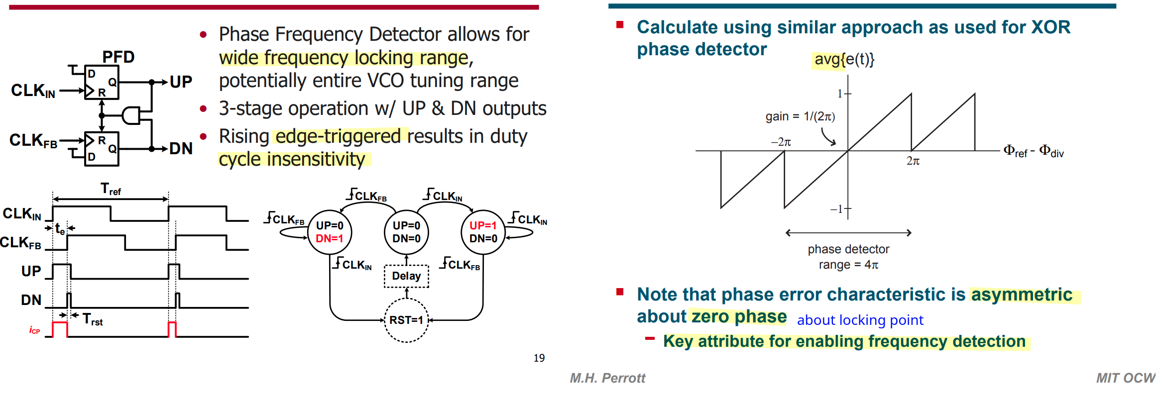
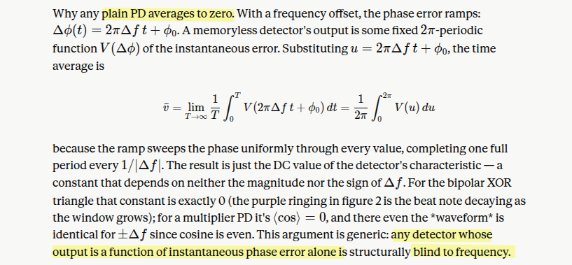
XOR Phase Detector
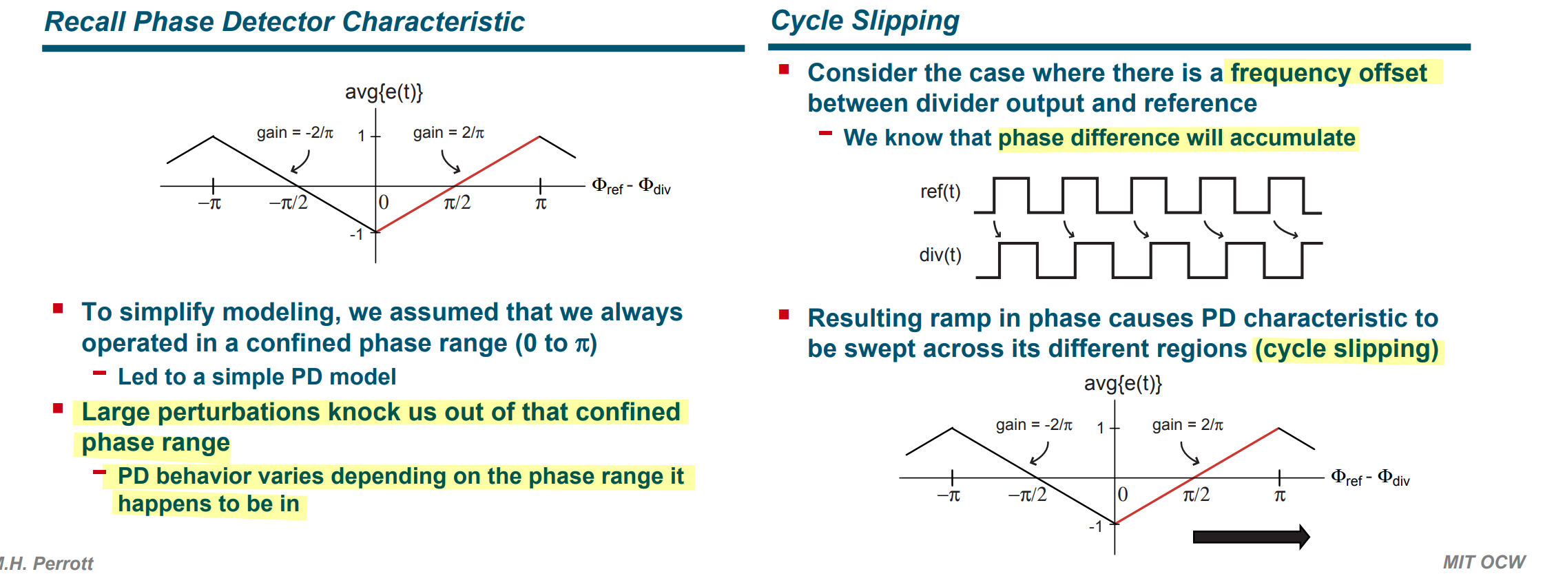
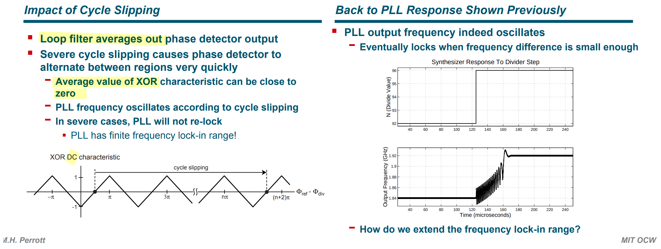
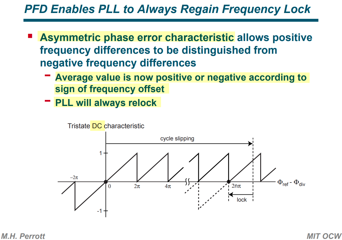
Cycle Slipping
Tristate PFD
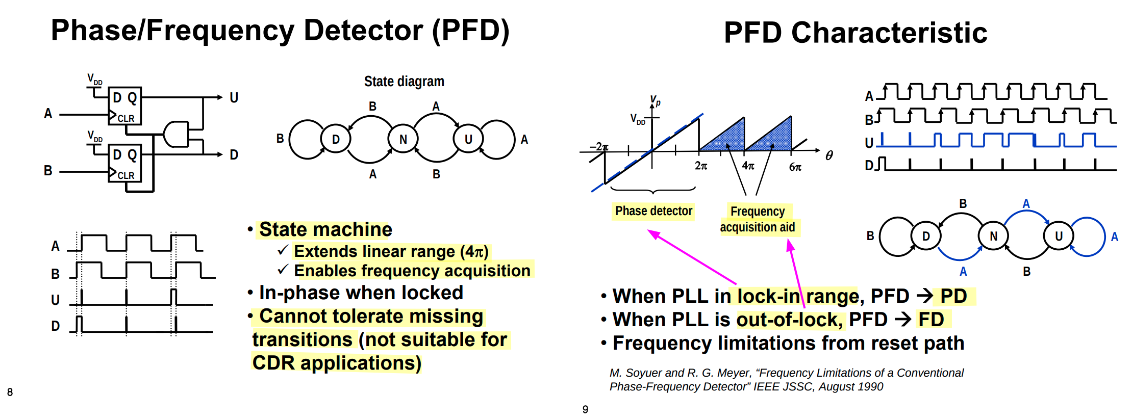
PFD requires periodic edges on both inputs
In a CDR, one input is random NRZ data, and a long run of identical bits has no transitions at all
The PFD's state machine interprets those missing edges as a huge phase/frequency error and pumps the loop away from lock
frequency acquisition
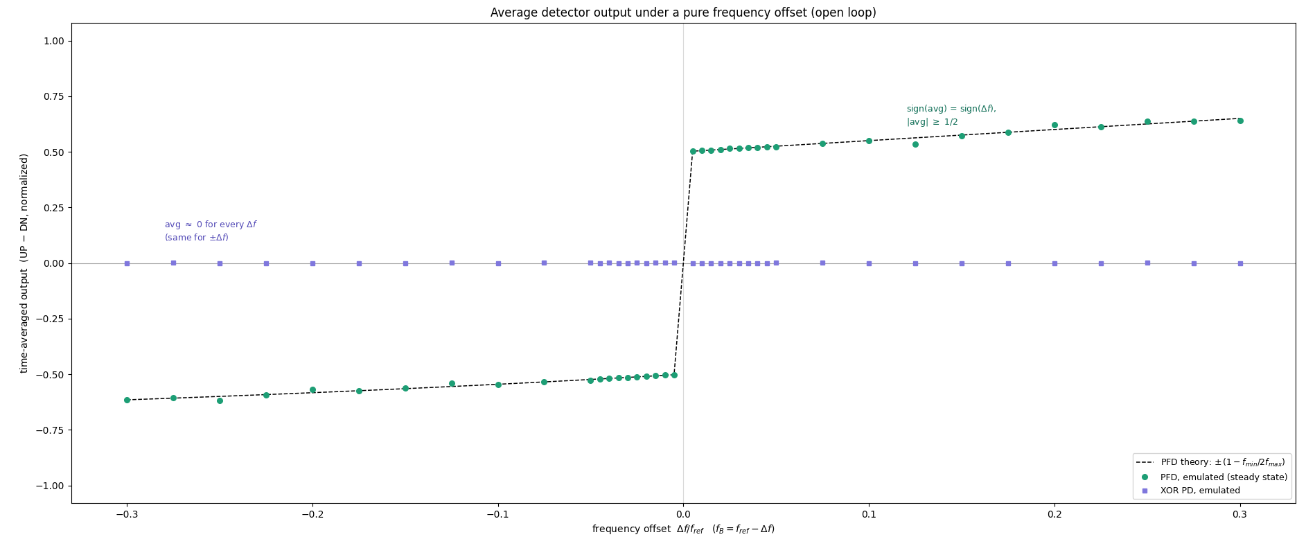
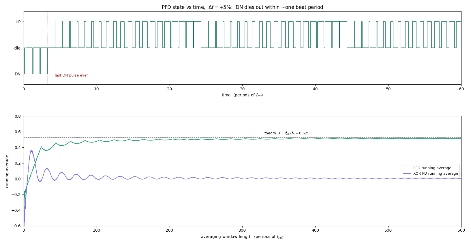
beat period: \(2\pi\cdot T_{beat,per}\cdot \Delta f = 2\pi \to T_{beat,per}=\frac{1}{\Delta f}\)
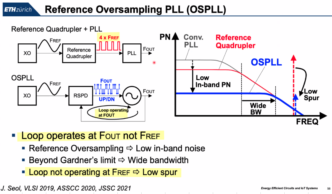
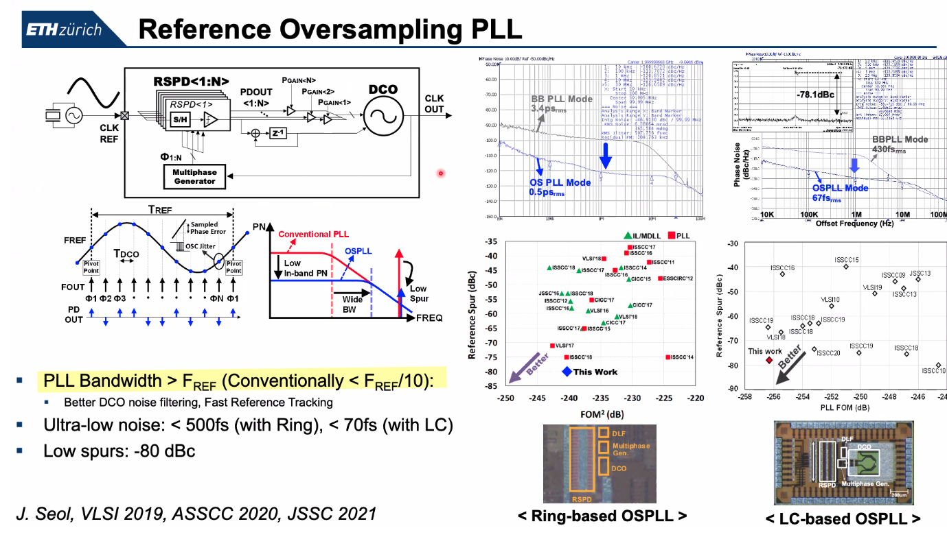
OSPLL (Reference Oversampling PLL)
J. -H. Seol, K. Choo, D. Blaauw, D. Sylvester and T. Jang, "Reference Oversampling PLL Achieving −256-dB FoM and −78-dBc Reference Spur," in IEEE Journal of Solid-State Circuits, vol. 56, no. 10, pp. 2993-3007, Oct. 2021 [https://sci-hub.se/10.1109/JSSC.2021.3089930]
Taekwang Jang SSCS DL talk : Ultra-low noise Phase-locked Loop Technique
K. J. Wang, A. Swaminathan and I. Galton, "Spurious Tone Suppression Techniques Applied to a Wide-Bandwidth 2.4 GHz Fractional-N PLL," in IEEE Journal of Solid-State Circuits, vol. 43, no. 12, pp. 2787-2797, Dec. 2008 [https://sci-hub.se/10.1109/JSSC.2008.2005716]
Frequency Divider
Gunnman, Kiran, and Mohammad Vahidfar. Selected Topics in RF, Analog and Mixed Signal Circuits and Systems. Aalborg: River Publishers, 2017
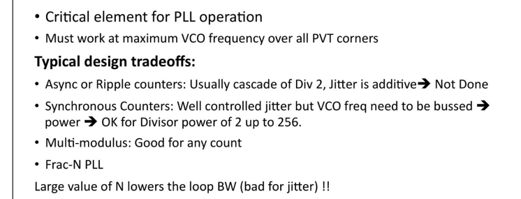
Large values of N lowers the loop BW which is bad for jitter
MMD (Multimodulus Divider)
TODO 📅
Noise in dividers (jitter generation)
S. Levantino, L. Romano, S. Pellerano, C. Samori and A. L. Lacaita, "Phase noise in digital frequency dividers," in IEEE Journal of Solid-State Circuits, vol. 39, no. 5, pp. 775-784, May 2004 [https://sci-hub.se/10.1109/JSSC.2004.826338]
Lacaita, Andrea Leonardo, Salvatore Levantino, and Carlo Samori. Integrated frequency synthesizers for wireless systems. Cambridge University Press, 2007.
TODO 📅
Enrico Rubiola. Phase Noise and Jitter in Digital Electronics [https://rubiola.org/pdf-slides/2016T-EFTF--Noise-in-digital-electronics.pdf]
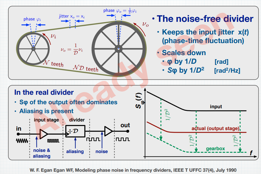
W. F. Egan, "Modeling phase noise in frequency dividers," in IEEE Transactions on Ultrasonics, Ferroelectrics, and Frequency Control, vol. 37, no. 4, pp. 307-315, July 1990 [https://sci-hub.se/10.1109/58.56498]
PLL + PSS + PNOISE convergence [https://community.cadence.com/cadence_technology_forums/f/custom-ic-design/48474/pll-pss-pnoise-convergence/1376833]
Signal Source Analyzer: measurement is based on time-average(or frequency-domain) method
real-time digital oscilloscope: measure sampled jitter directly
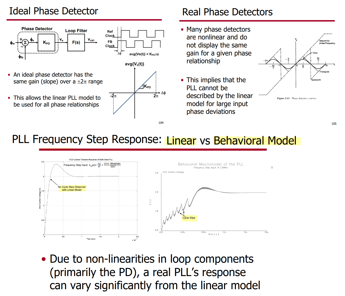
phase margin impact
type-I PLLs
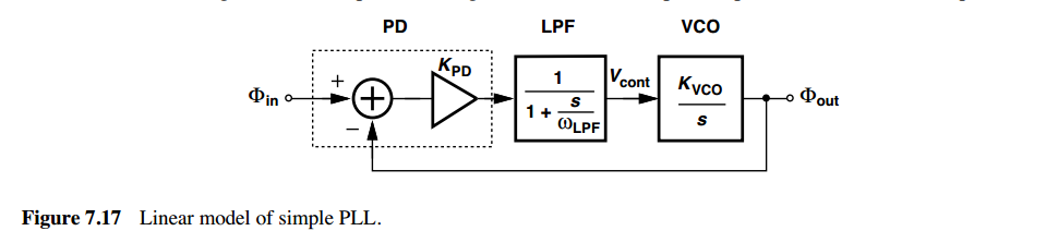
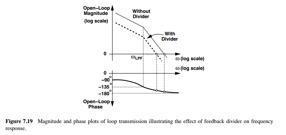
frequency divider weakens the feedback and increases the phase margin
type-II PLLs
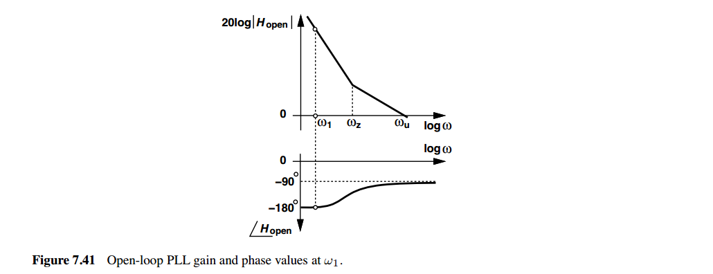
frequency divider weakens the feedback and decrease the phase margin
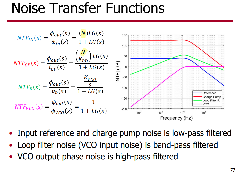
phase noise & jitter
[Timing 101: The Case of the Jitterier Divided-Down Clock, Silicon Labs]
[How division impacts spurs, phase noise, and phase]
[Phase Noise Theory: Ideal Frequency Multipliers and Dividers]
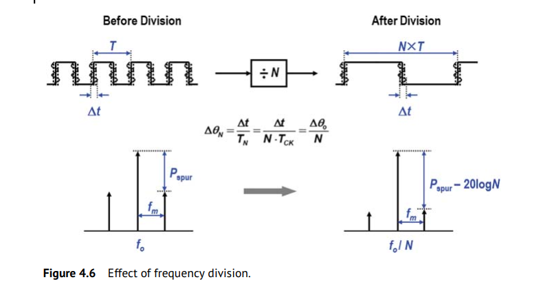
- Multiplying the frequency of a signal by a factor of N using an ideal frequency multiplier increases the phase noise of the multiplied signal by \(20\log(N)\) dB.
- Similarly dividing a signal frequency by \(N\) reduces the phase noise of the output signal by \(20\log(N)\) dB
The sideband offset from the carrier in the frequency multiplied/divided signal is the same as for the original signal.
\(20\log (N)\) Rule
If the carrier frequency of a clock is divided down by a factor of \(N\) then we expect the phase noise to decrease by \(20\log(N)\).The primary assumption here is a noiseless conventional digital divider.
The \(20\log(N)\) rule only applies to phase noise and not integrated phase noise or phase jitter. Phase jitter should generally measure about the same.
What About Phase Jitter?
We integrate SSB phase noise L(f) [dBc/Hz] to obtain rms phase jitter in seconds as follows for “brick wall” integration from f1 to f2 offset frequencies in Hz and where f0 is the carrier or clock frequency.
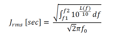
Note that the rms phase jitter in seconds is inversely proportional to f0. When frequency is divided down, the phase noise, L(f), goes down by a factor of 20log(N). However, since the frequency goes down by N also, the phase jitter expressed in units of time is constant.
Therefore, phase noise curves, related by 20log(N), with the same phase noise shape over the jitter bandwidth, are expected to yield the same phase jitter in seconds.
Effective Divide Ratio
Sam Palermo, ECEN620: Network Theory Broadband Circuit Design Fall 2025, Lecture 10: Fractional-N Frequency Synthesizers [https://people.engr.tamu.edu/spalermo/ecen620/lecture10_ee620_fracn_freq_synth.pdf]
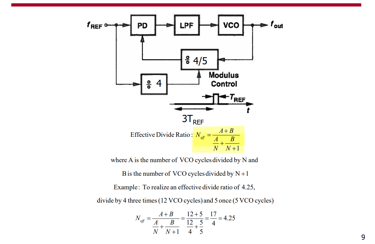
with \(M_{ref}\), the number of reference clock cycles \[ A\cdot \frac{T_{ref}}{N} + B\cdot \frac{T_{ref}}{N+1} = M_{ref} T_{ref} \qquad N_{vco} = A +B \]
yield effective divide ratio \[ N_{eff} = \frac{N_{vco}}{M_{ref}} = \boxed{ \frac{A+B}{\frac{A}{N} + \frac{B}{N+1}} } = \textcolor{red}{\frac{\frac{A}{N}}{\frac{A}{N} + \frac{B}{N+1}}}\cdot N + \textcolor{blue}{\frac{\frac{B}{N+1}}{\frac{A}{N} + \frac{B}{N+1}}}\cdot (N+1) \]
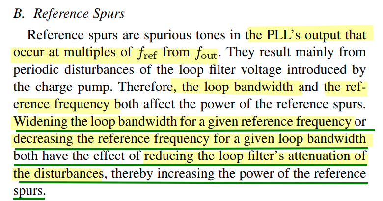
Reference Spur
spurs are carrier or clock frequency spectral imperfections measured in the frequency domain just like phase noise. However, unlike phase noise they are discrete frequency components.
Spurs are deterministic
Spur power is independent of bandwidth
Spurs contribute bounded peak jitter in the time domain
Sources of Spurs:
- External (coupling from other noisy block) Supply, substrate, bond wires, etc.
- Internal (int-N/fractional-N operation)
- Frac spur: Fractional divider (multi-modulus and frequency accumulation)
- Ref. spur: PFD/charge pump/analog loop filter non-idealities, clock coupling
Integer-N PLL
integer-N PLL frequency synthesizers
the frequency resolution, is equal to the reference frequency, meaning that only integer multiples of the reference frequency can be synthesized
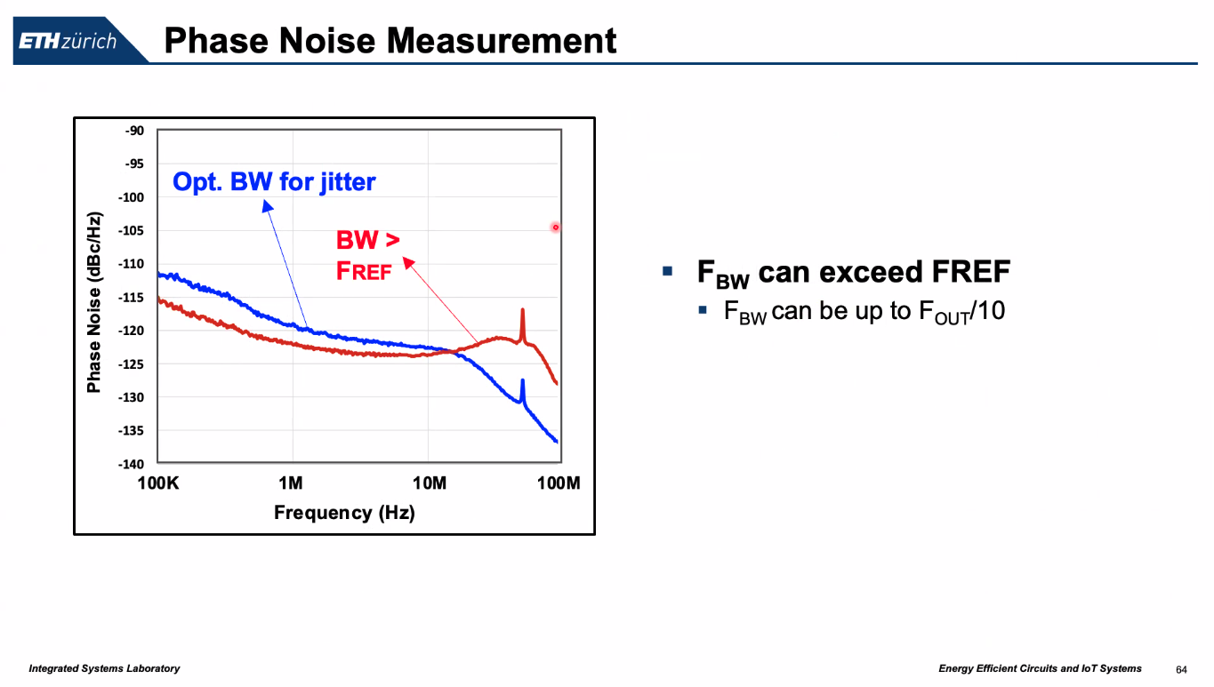
Stability requirements limit the loop bandwidth to about one tenth of the reference frequency; therefore
- decreasing the reference frequency increases the settling time as the loop bandwidth also has to be decreased
- a reduced loop bandwidth allows less suppression of the VCO’s inherent phase noise
Another drawback of the integer-N PLL is the trade-off between phase noise and settling time when the divider ratio becomes large (The contributions to the output phase noise of almost all PLL building blocks, except the VCO, are multiplied by the division ratio)
[https://people.engr.tamu.edu/spalermo/ecen620/lecture03_ee620_pll_system.pdf]
if a small reference frequency is chosen, the reference spur in the output phase noise is located at a smaller offset frequency
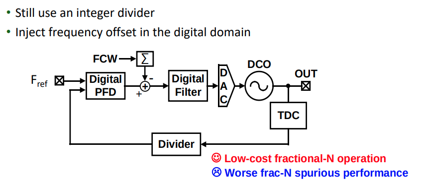
Fractional-N
- Dither Feedback Divider Ratio by a delta-sigma modulator
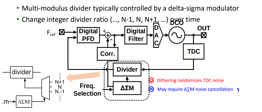
- Frequency Accumulation
Switched Capacitor Banks
Q: why \(R_b\) ?
A: TODO 📅
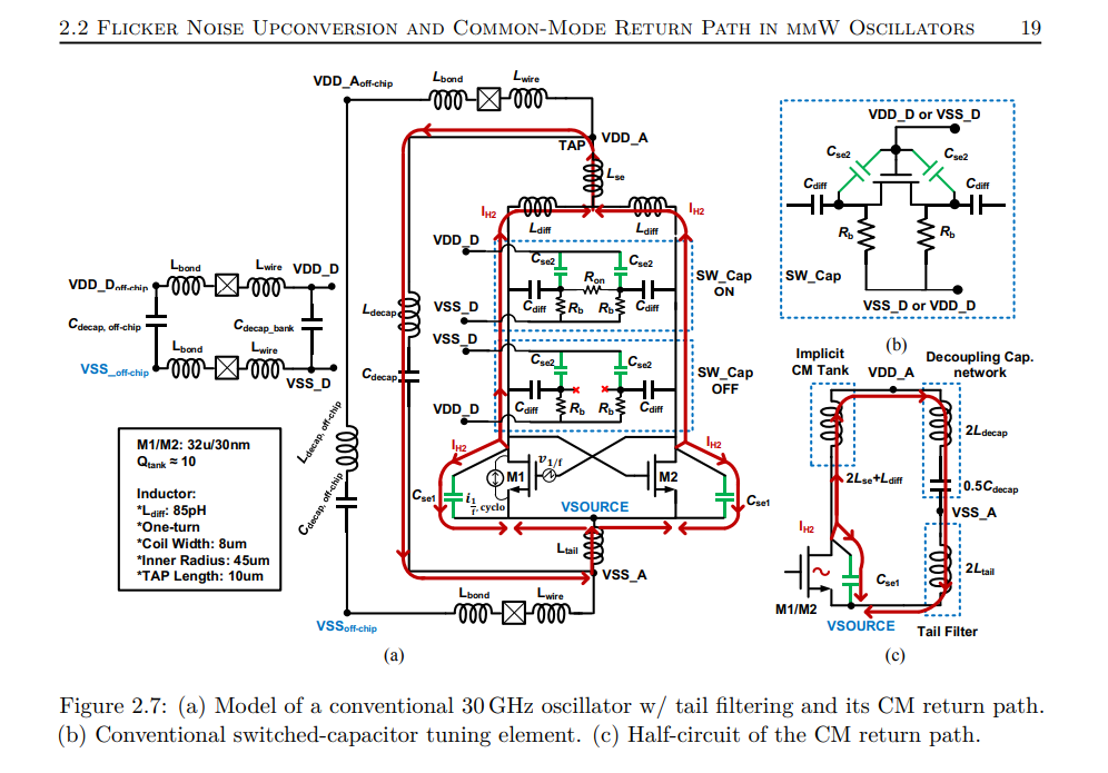
Hu, Yizhe. "Flicker noise upconversion and reduction mechanisms in RF/millimeter-wave oscillators for 5G communications." PhD diss., 2019.
S. D. Toso, A. Bevilacqua, A. Gerosa and A. Neviani, "A thorough analysis of the tank quality factor in LC oscillators with switched capacitor banks," Proceedings of 2010 IEEE International Symposium on Circuits and Systems, Paris, France, 2010, pp. 1903-1906
False locking
TODO 📅
- divider failure
- even-stage ring oscillator ( multipath ring oscillators)
- DLL: harmonic locking, stuck locking
clock edge impact

ck1 is div2 of ck0
edge of ck0 is affected differently by ck1
edge of ck1 is affected equally by ck0
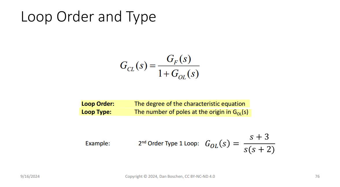
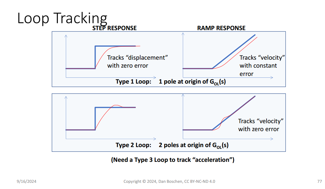
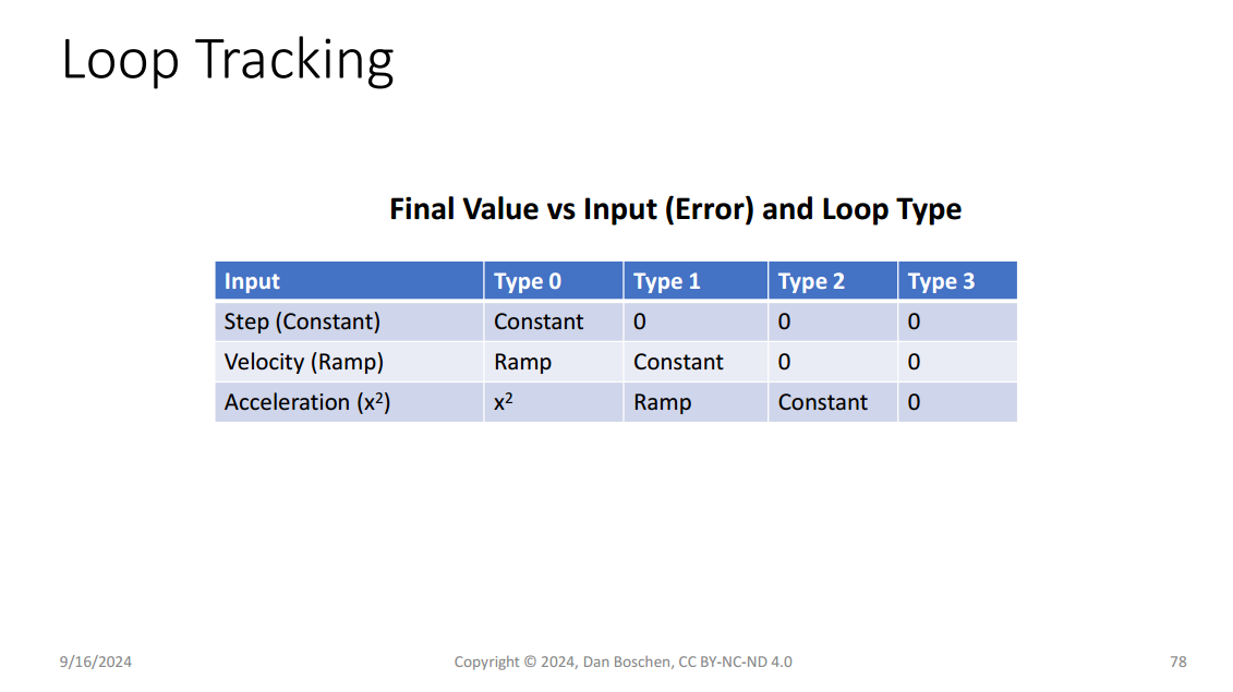
Why Type 2 PLL ?
Type: # of integrators within the loop
Order: # of poles in the closed-loop transfer function
Type \(\leq\) Order
- That is, to have a wide bandwidth, a high loop gain is required
- More importantly, the type 1 PLL has the problem of a static phase error for the change of an input frequency
Type 1 PLL with input phase step \(\Delta \phi \cdot u(t)\) \[\begin{align} \Delta \phi\cdot u(t) - K\int_0^{t}\phi _e (\tau)d\tau &= \phi _e (t) \\ \phi _e (0) &= \Delta \phi \end{align}\]
we obtain \(\phi _e (t) = \Delta \phi \cdot e^{-Kt}\cdot u(t)\)
and \(\phi _e(\infty) = 0\)
Daniel Boschen. GRCon24 - Quick Start on Control Loops with Python Workshop [https://events.gnuradio.org/event/24/contributions/599/attachments/187/480/Boschen%20Control%20Presentation.pdf]
Ring Oscillators and Process Variations
Inverter-19 - Ring Oscillators and Process Variations [https://youtu.be/b1xZU0aD4hA]
IC_designer, VCO cali [link]

we have
\[ (N+\Delta) T_o = MT_r\quad \Delta\in [-1,1] \]
then,
\[ f_o = \frac{N}{M}f_r\color{red}\left(1+\frac{\Delta}{N}\right) \]
\(\frac{\Delta}{N}\) determine measurement accuracy, \(\frac{\Delta}{N} \lt 0.01\) if 1% accuracy is needed
PLL Characterization
PLL bandwidth by step stimulus
[How can I experimentally find the bandwidth of my PLL?, https://dsp.stackexchange.com/a/73654/59253]
A step response test is an easy way to determine the bandwidth.
Sum a small step into the control voltage of your oscillator (VCO or NCO), and measure the 90% to 10% fall time of the corrected response at the output of the loop filter as shown in this block diagram
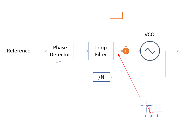
a first order loop \[ BW = \frac{0.35}{t} \space\space\space\space \text{(first order system)} \] Where \(BW\) is the 3 dB bandwidth in Hz and \(𝑡\) is the 10%/90% rise or fall time.
For second order loops with a typical damping factor of 0.7 this relationship is closer to: \[ BW = \frac{0.33}{t}\space\space\space\space \text{(second order system, damping factor = 0.7)} \]
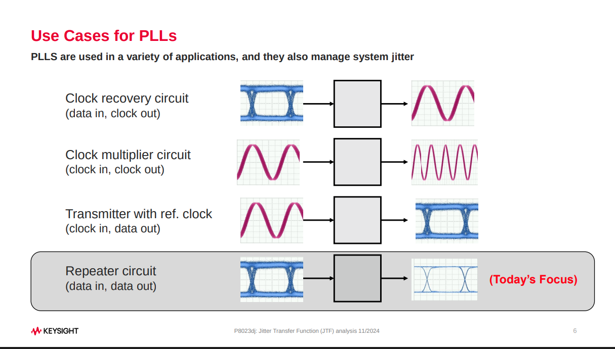
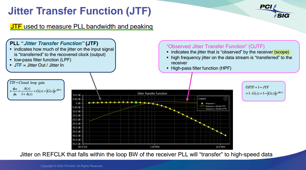
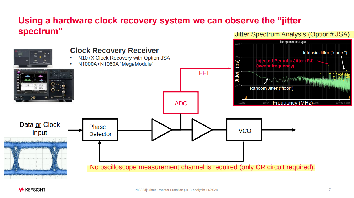
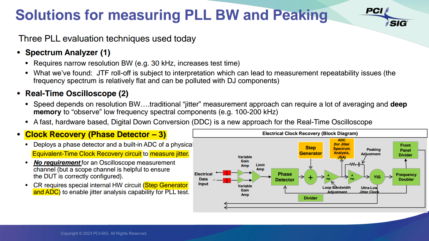
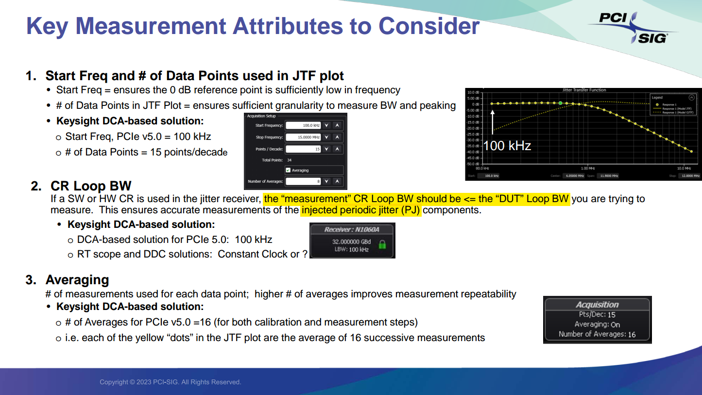
PLL BW and peaking by Clock Recovery Method
Rick Eads Principal Planner, Keysight Technologies, PLL Characterization Techniques for High Precision Measurement
John Calvin, Jitter Transfer Function (JTF) analysis Version 1.0 Presented to IEEE P802.3dj Task Force 11/11/2024 [https://grouper.ieee.org/groups/802/3/dj/public/24_11/calvin_3dj_01_2411.pdf]
Michael Schnecker, Clock Recovery Methods for Jitter Analysis [https://cdn.teledynelecroy.com/files/whitepapers/wp_clock_recovery.pdf]
—, DesignCon 2009 Jitter Transfer Measurement in Clock Circuits [https://cdn.teledynelecroy.com/files/whitepapers/designcon2009_lecroy_jitter_transfer_measurement_in_clock_circuits.pdf]
N1076B/7A/7B/8A DCA-M Optical and electric clock data recovery solutions [https://www.keysight.com/us/en/assets/7018-05291/data-sheets/5992-1620.pdf]
reference
Dennis Fischette, Frequently Asked PLL Questions [https://www.delroy.com/PLL_dir/FAQ/FAQ.htm]
Ian Galton, ISSCC 2010 SC3: Fractional-N PLLs [https://www.nishanchettri.com/isscc-slides/2010%20ISSCC/Short%20Course/SC3.pdf]
Mike Shuo-Wei Chen, ISSCC 2020 T6: Digital Fractional-N Phase Locked Loop Design [https://www.nishanchettri.com/isscc-slides/2020%20ISSCC/TUTORIALS/T6Visuals.pdf]