analog design environment
noiseon & noiseoff
Options -> Analog...
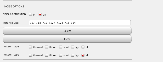
only work in presimu simulation (excluding lpe.spi)
vsource with noisefile
- both rise/fall edge are added the noisefile
- noise between rise and fall edge are partially correlated
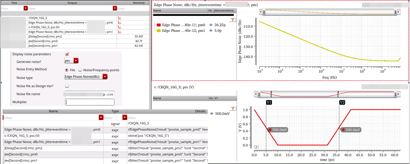
Pnoise sampled(jitter) with Sampled Phase
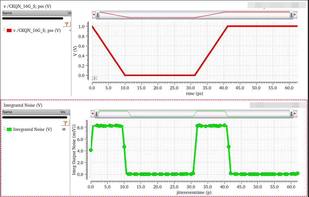
vsource output is applied with noise all the time
Loockup Table vs Equations Model in Verilog-A
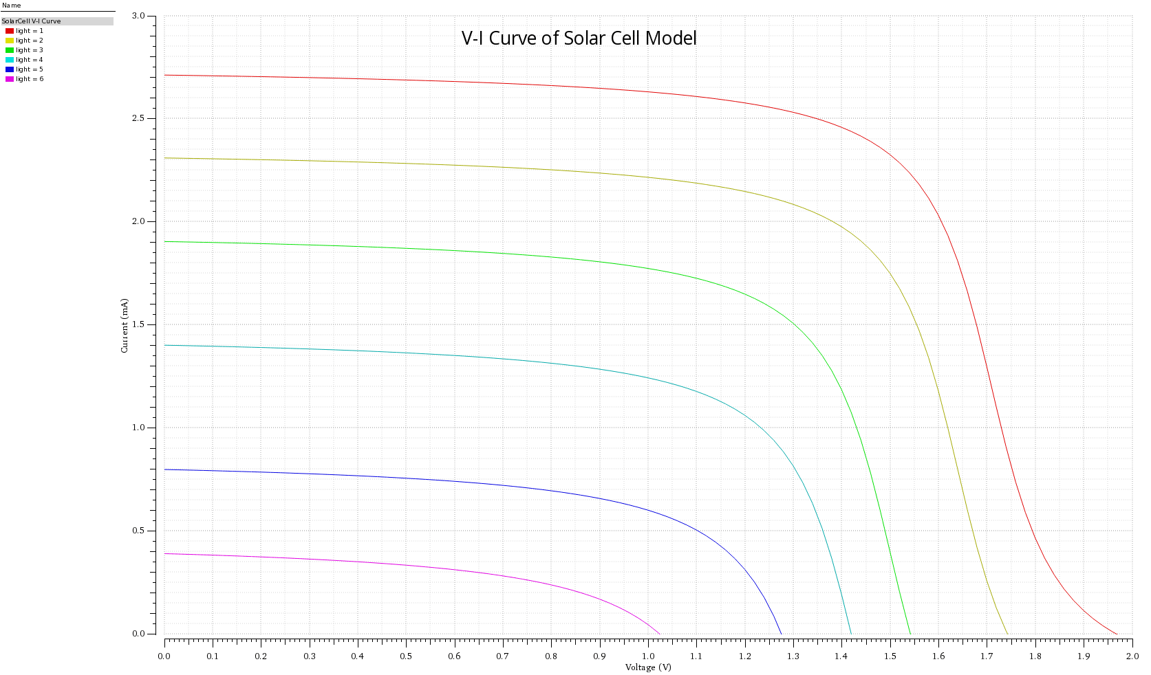
Solar Cell Verilog Model for Cadence [https://miscircuitos.com/solar-cell-verilog-model-for-cadence/]
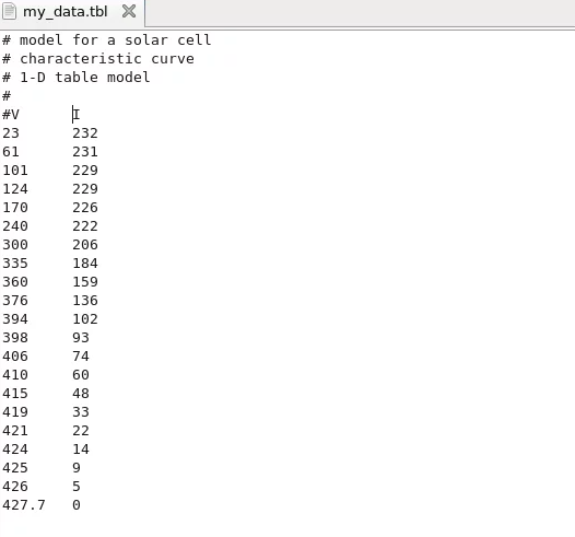
How to Create a new Cell in Cadence with a Loockup Table Model in Verilog-A [https://miscircuitos.com/how-to-create-a-model-in-verilog-a-with-a-lockup-table/]
with Equation
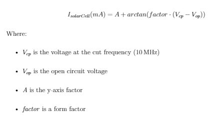
1 | ///////////////////////////////////////////////////////////////////////////// |
with lookup table
1 | /////////////////////////////////////////////////////////////////////////// |
PEX LAYER_MAP
1 | // *LAYER_MAP |
[https://picture.iczhiku.com/resource/eetop/wYItYWLPleWrpvNV.pdf]
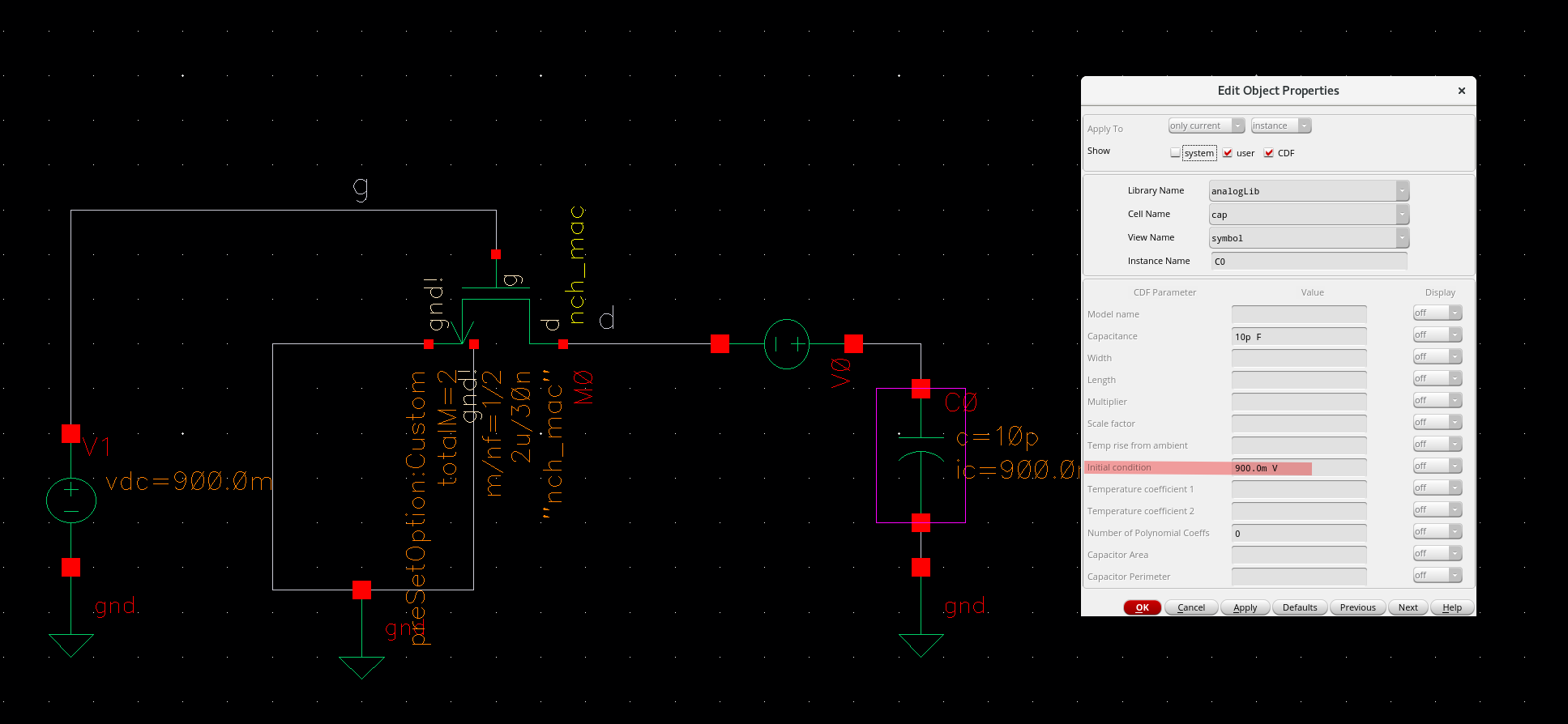
nodeset & initial condition
A nodeset steers the convergence in a particular direction - useful to speed up DC convergence
An initial condition is useful when you want to force the circuit to start a transient in a particular condition
Remove prefix from multiple files in Linux console
Bash
1 | for file in prefix*; do mv "$file" "${file#prefix}"; done; |
The for loop iterates over all files with the prefix. The do removes from all those files iterated over the prefix.
Here is an example to remove "bla_" form the following files:
1 | bla_1.txt |
Command
1 | for file in bla_*; do mv "$file" "${file#bla_}";done; |
Result in file system:
1 | 1.txt |
[https://gist.github.com/guisehn/5438bbc22138435665c6e996493fe02b]
remove .cdslck
1 | #!/bin/sh |
[https://wikis.ece.iastate.edu/vlsi/index.php?title=Tips_%26_Tricks#Locked_Files_in_Cadence]
Custom Bindkey
schBindKeys.il
schematic
1 | alias bk hiSetBindKey |
leBindKeys.il
layout
1 | alias bk hiSetBindKey |
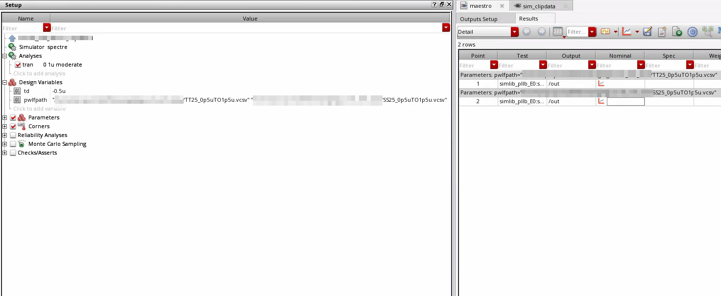
Design Variable in vpwlf
PWL File as Design Var? parameter in vpwlf cell
is convenient for sweep simulation or corner simulation, wherein there
are multiple pwl files .
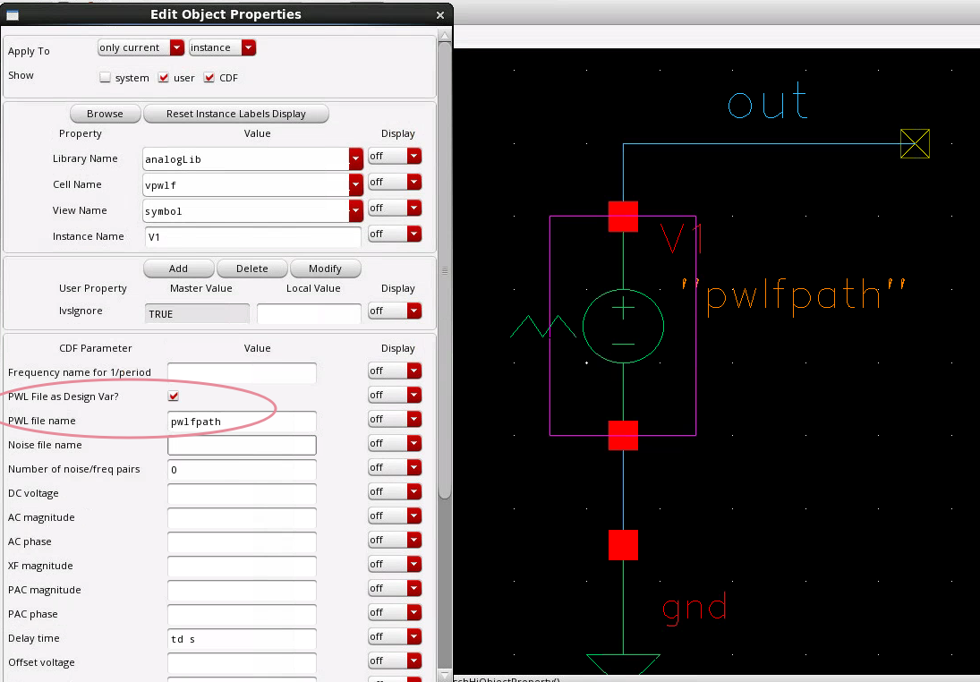
The file path should be surrounded with double-quotes to be protected from evaluation.
save option
none:
Does not save any data (currently does save one node chosen at random)
selected:
Saves only signals specified with save statements. The default setting.
lvlpub:
Saves all signals that are normally useful up to nestlvl deep in the subcircuit hierarchy. This option is equivalent to allpub for subcircuits.lvl:
Saves all signals up to nestlvl deep in the subcircuit hierarchy. This option is relevant for subcircuits.
allpub:
Saves only signals that are normally useful.
all:
Saves all signals.
Signals that are "normally useful" include the shared node voltages and currents through voltage sources and iprobes, and exclude the internal nodes on devices (the internal collector, base, emitter on a BJT, the internal drain, source on a FET, and so on). It also excludes currents through inductors, controlled sources, transmission lines, transformers, etc.
If you use lvl or all instead of lvlpub or allpub, you will also get internal node voltages and currents through other components that happen to compute current.
Thus, using *pub excludes internal nodes on devices (the internal collector, base, emitter on a BJT, the internal drain and source on a FET, etc). It also excludes the currents through inductors, controlled sources, transmission lines, transformers, etc.
nestlvl
This variable is used to save groups of signals as results and when signals are saved in subcircuits. The nestlvl parameter also specifies how many levels deep into the subcircuit hierarchy you want to save signals.
virtuoso "dlopen failed to open 'libdl.so'"
1 | $ sudo yum install glibc-devel |
1 | Last metadata expiration check: 0:01:02 ago on Sat 24 Sep 2022 12:13:54 AM CST. |
SpiceIn foundary's standard cell's spice netlist
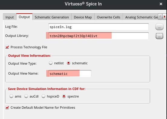
use SpiceIn GUI feature to map MOS parameter correctly in generated schematic
Input
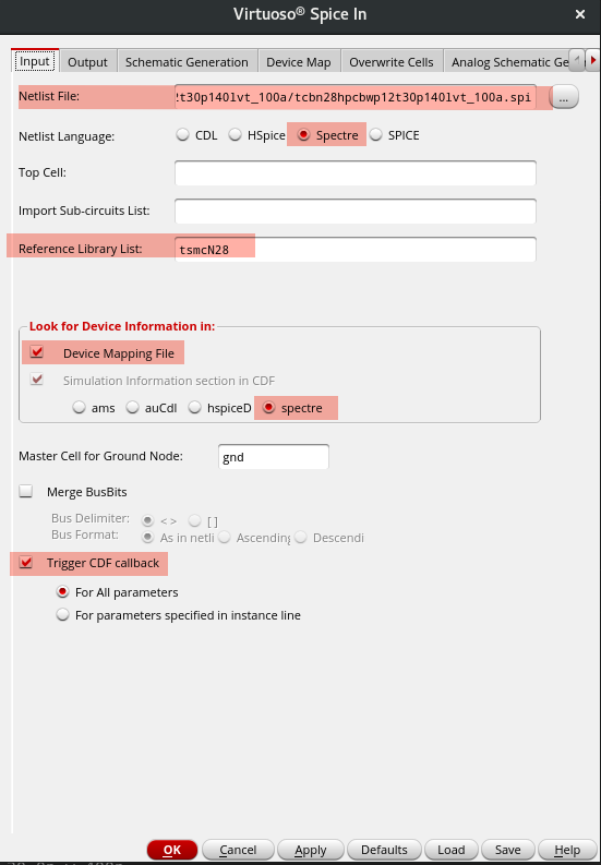
The mos's total width (parameter name "w") value will update during SpiceIn trigger CDF callback automatically
Output
Device Map
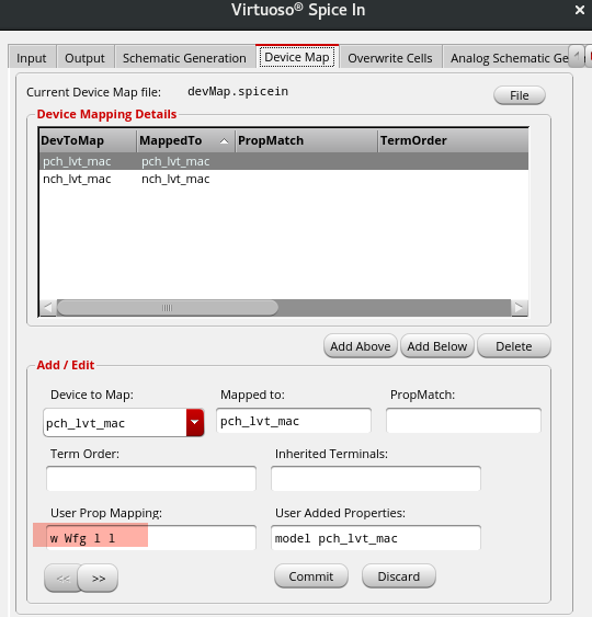
User Prop Mapping is significant setup, both xxx.spi and Edit CDF provide the essential information.
The map syntax is spice_para0 cdf_para0 spice_para1 cdf_para01 ... spice_paraN cdf_paraN
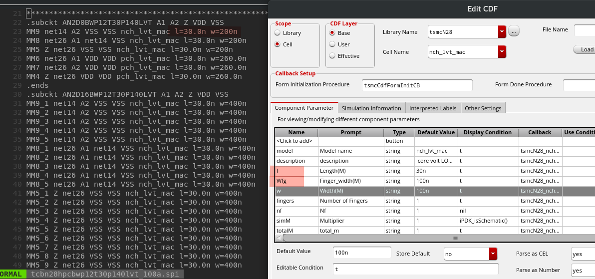
reference
Article (20488179) Title: How to use SpiceIn GUI feature to map MOS parameter correctly in generated schematic URL: https://support.cadence.com/apex/ArticleAttachmentPortal?id=a1O3w000009bdPWEAY
Article (11724692) Title: SpiceIn maps the netlist parameter to the CDF parameter incorrectly on the generated schematic devices (e.g. w to wf) URL: https://support.cadence.com/apex/ArticleAttachmentPortal?id=a1Od0000000nZ2CEAU
Model Library Setup
In order to set up model files automatically in the Model Library Setup form for Spectre or AMS simulator in ADE Explorer or ADE Assembler
Add the following line in your .cdsinit
1 | envSetVal( "spectre.envOpts" "modelFiles" 'string "<path_to model_file>/myModels.scs") |
or
1 | envSetVal("spectre.envOpts" "modelFiles" 'string "moreModels;ff mymodels;tt") |

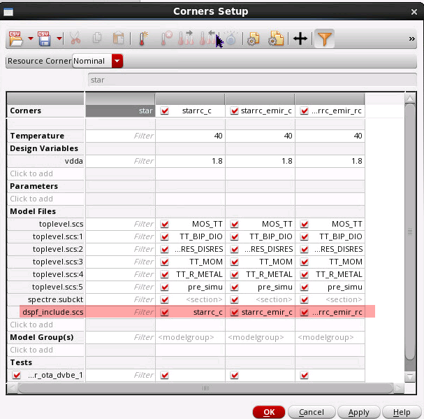
DSPF for each corner
Create a new file with an extension scs like myDSPF_Files.scs
1 | * DSPF files to use with Corner Definitions |
Add the file created above ‘myDSPF_File.scs’ in ‘Add/Edit Model Files’ of Corners setup form
split pins in dspf_emir
dspf extract using starrc
multiple label and rectangle in vssa net

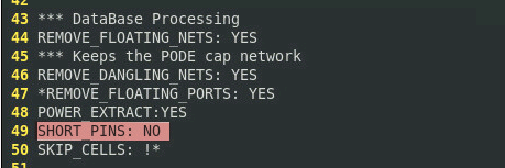
general dspf
SHORT_PINS: YES
other pin are short together
dspf for emir analysis


It seems that dspf_emir don't contain the rectangle pin information.
only label is necessary
| setup | spectre result | ||
|---|---|---|---|
| netlist type | dspf option | emir analysis | |
| dspf | / | disable | ✓ |
| dspf_emir | / | disable | ✗ |
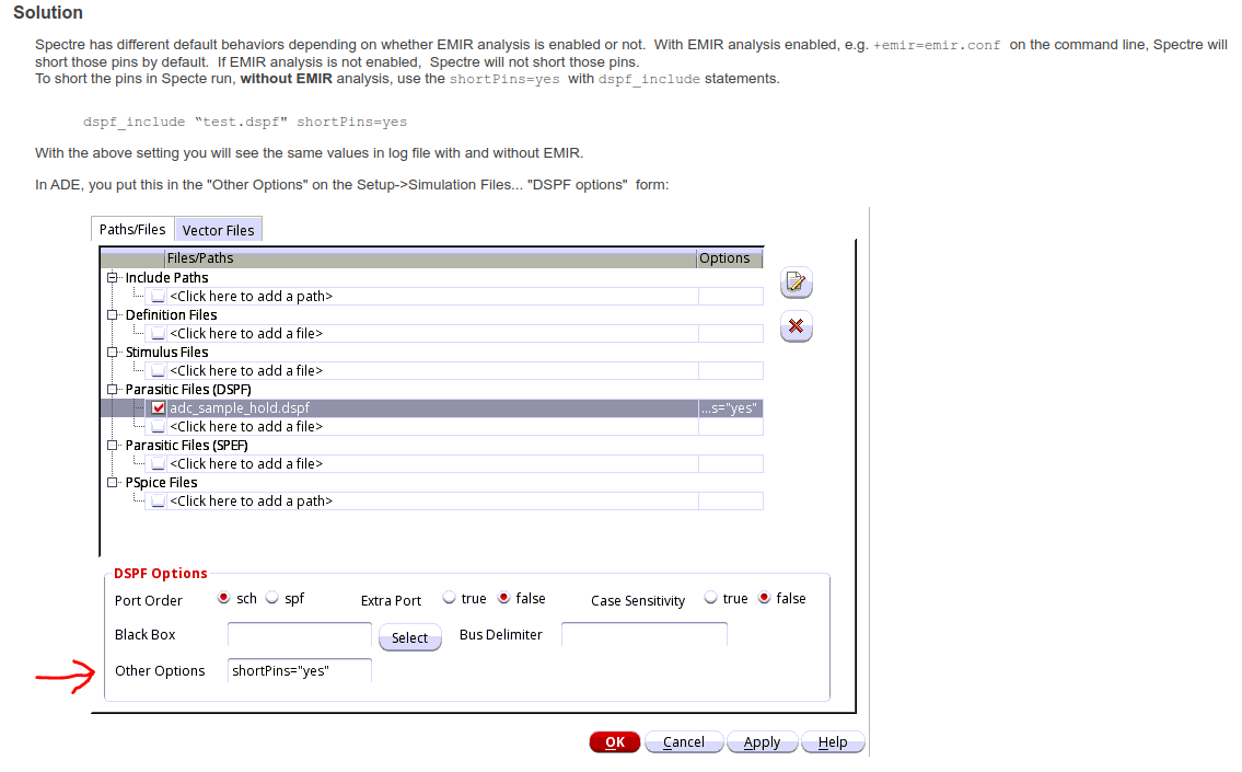
| dspf_emir | =shortPins=”yes” | disable | ✓ |
| dspf_emir | =shortPins=”no” | disable | ✗ |
| dspf_emir | / | enable | ✓ |
| dspf_emir | =shortPins=”yes” | enable | ✓ |
| dspf_emir | =shortPins=”no” | enable | ✓ |
shortPins=”yes” is preferred default option for dspf_emir, which has split pins
DSPF Syntax
::=*|P ? describes pins in the net. Multiple pin descriptions can be listed in one line. ::=( { }?) represents the name of the pin. represents the type of the pin. It can be any of the following: I (Input), O (Output), B (Bidirectional), X (don’t care), S (Switch), and J (Jumper).
represents the capacitance value associated with the pin. is optional. It represents the location of the pin. Multiple pin locations are allowed
split pins
1 | *|P (avss_1 O 0 207.7555 59.9170) |
reference
Article (20467964) Title: Difference in result on running Spectre APS with EMIR and without EMIR analysis URL: https://support.cadence.com/apex/ArticleAttachmentPortal?id=a1O0V00000679GRUAY
StarRC User Guide and Command Reference Version O-2018.06, June 2018
DSPF Options
Case Sensitivity
| netlist format | default option |
|---|---|
| Spectre netlist | case sensitive |
| dspf format | case insensitive |
For a dspf format, it will be treated as a spice netlist format, which is by default case insensitive
Pay attention to VerilogIn block, which may contain upper case / lower case net name, e.g NET1 and net1.
The extracted DSPF using extraction tool also contain NET1 and net1, which shall not be shorted together.

Port Order
If you use
.dspf_include, the following rules apply:
- The subcircuit description is taken from the DSPF file even if the same subcircuit description is available in the schematic netlist.
- Depending on the
port_orderoption, the port order of the subcircuit definition is taken from the pre-layout schematic netlist or from the DSPF file subcircuit definition, as shown below.
port_order=sch– (Default). The port order is taken from schematic subcircuit definition. The same port number and names are required. If the schematic subcircuit definition is not available, a warning is issued in the log file, and DSPF port order is used.port_order=spf– The port order is taken from the DSPF subcircuit definition.
SPICE_SUBCKT_FILE of StarRC
The StarRC tool reads the files specified by the SPICE_SUBCKT_FILE command to obtain port ordering information. The files control the port ordering of the top cell as well. The port order and the port list members read from the .subckt for a skip cell are preserved in the output netlist.
The file usually is the cdl netlist of extracted cell, this way, port order is not problem
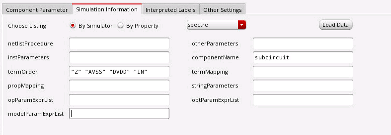
CDF termOrder
DSPF same order
DSPF
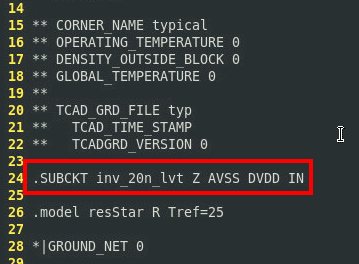
input.scs

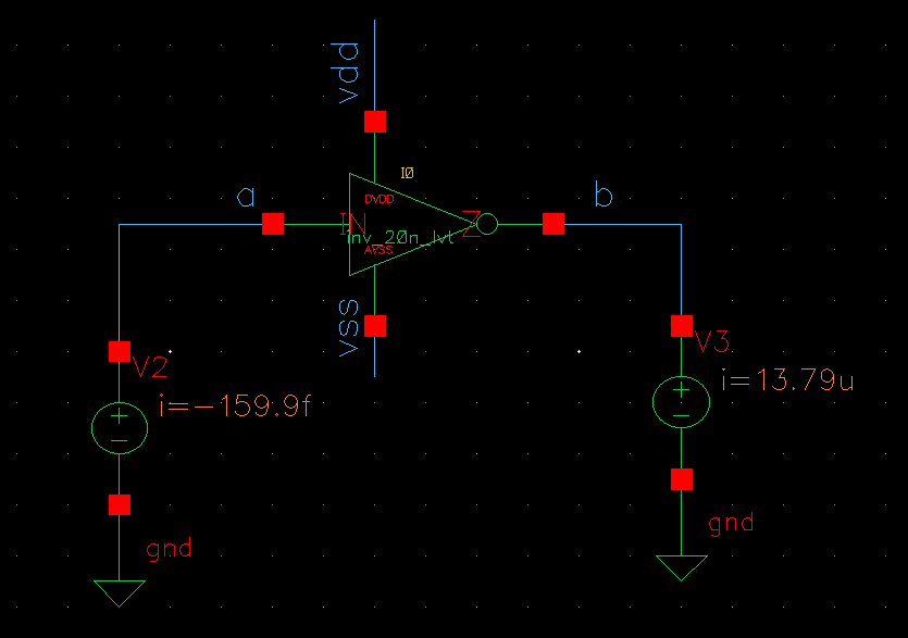
different order
manual change DSPF's pin order shown as below

port_order=sch
dspf port is mapping to schematic by name, and the simulation result is right
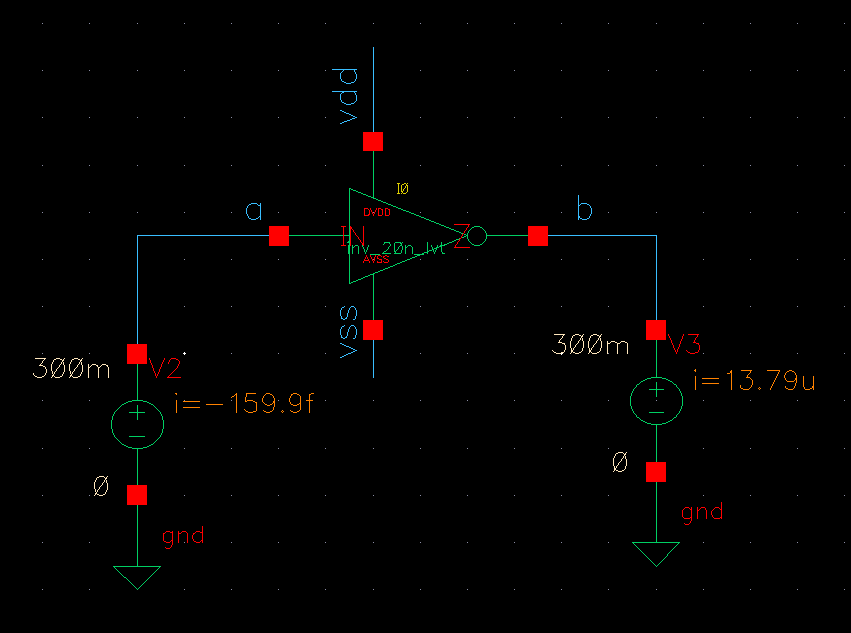
port_order=spf
dspf pin order is retained, and no mapping between spectre netlist and dspf.
The simulation result is wrong
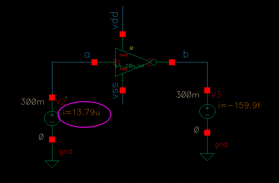
bus_delim="_ <>"
The way this works is that the first part of bus_delim is the "schematic" delimiter (i.e. what's in the spectre netlist), and the other part is the DSPF delimiter
reference
Article (20502176) Title: How does Spectre understand case-sensitive net names when using various post-layout netlists such as dspf, av_extracted view, or smart view? URL: https://support.cadence.com/apex/ArticleAttachmentPortal?id=a1O3w000009fthoEAA
spf in cadence https://community.cadence.com/cadence_technology_forums/f/custom-ic-design/31326/spf-in-cadence/1342278#1342278
Spectre Tech Tips: Using DSPF Post-Layout Netlists in Spectre Circuit Simulator - Analog/Custom Design - Cadence Blogs - Cadence Community https://shar.es/afO6e1
StarRC™ User Guide and Command Reference Version O-2018.06, June 2018
Virtual Connectivity
Normally, if the layout connectivity extractor finds disjoint, unconnected geometries with the same net name text attached, the extractor will view this as an open circuit.
- Virtual connection results in the extraction of a single net from two or more disjoint physical nets when the physical net segments share the same name.
- Virtual connectivity is triggered by the rule file VIRTUAL CONNECT COLON and VIRTUAL CONNECT NAME specification statements.
- Virtual connectivity can also be specified through the Calibre Interactive GUI.
VIRTUAL CONNECT COLON
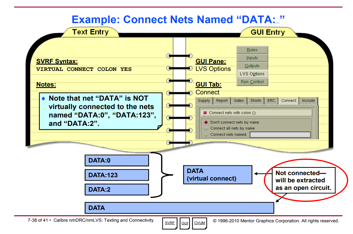
Virtual Connect Colon is used to virtually connect nets that share a common prefix before a colon, like VDD:1, VDD:2, and so forth.
If you specify YES, then the connectivity extractor first strips off all characters from the first colon to the end of the label names.
Next, the extractor forms a virtual connection between any two labels that have the same name and that originally contained a colon.
Colons can appear anywhere in the name with the exception that a colon at the beginning of a name is treated as a regular character (that is, it has no special effect).
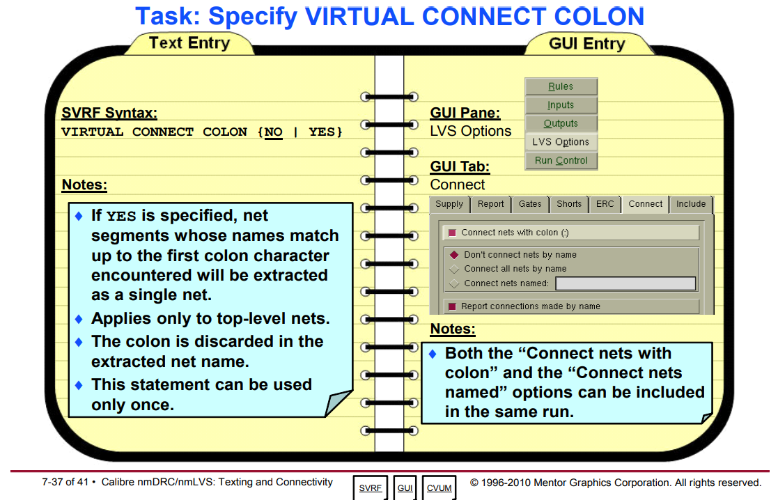
up to the first colon character encountered
The colon is discarded in the extracted net name
VIRTUAL CONNECT NAME
Virtual Connect Name virtually connects nets that share the same name
Each name is a net name and can be optionally enclosed in quotes.
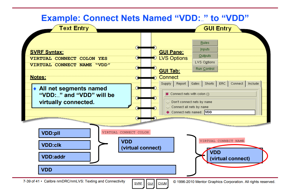
The connectivity extractor forms a virtual connection between any two labels having the same name such that the label name appears in a Virtual Connect Name specification statement in the rule file.
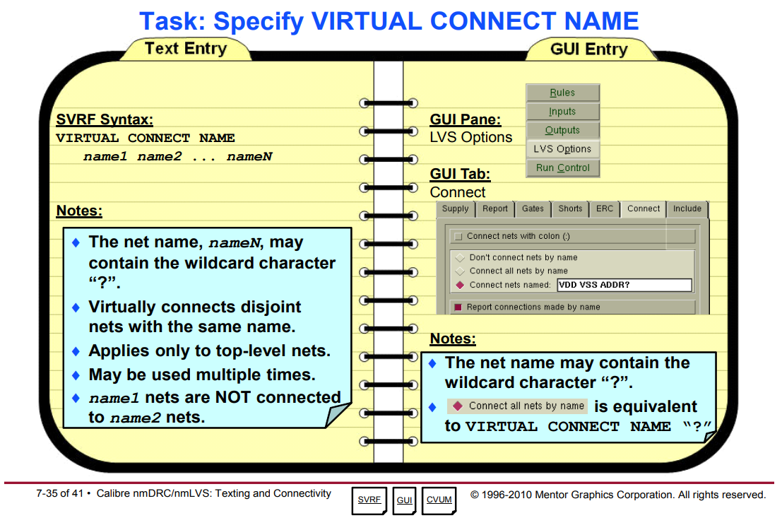
VIRTUAL CONNECT NAME ?== Connect all nets by name
Note that if Virtual Connect Colon YES is also specified, then Virtual Connect Name operates on names after all colon suffixes have been stripped off.
reference
Calibre Fundamentals: Performing DRC/LVS Student Workbook
Calibre Verification User’s Manual Software Version 2019.3 Document Revision 7
Calibre Runsets
Calibre Interactive stores a list of your most recently opened
runsets in your home directory as .cgidrcdb or
.cgilvsdb for Calibre Interactive DRC or LVS,
respectively.
When invoked, the Calibre DRC and LVS windows automatically load the runset used when the last session was closed.
Runsets are ASCII files that set up Calibre Interactive for a Calibre run. They contain only information that differs from the default configuration of Calibre Interactive. There is a one-to-one correspondence between entry lines in the runset file and fields and button items in the Calibre Interactive user interface. Here is as example of a DRC runset:
2
3
4
5
6
7
8
9
10
11
*drcRulesFileLastLoad: 1009224452
*drcLayoutPaths: ./lab3.gds
*drcLayoutPrimary: lab3
*drcResultsFile: ./lab3.db
*drcSummaryFile: drc_report
*drcRunTurbo: 0
*drcRunRemoteOn: Cluster
*drcRemoteLICENSEFILEName: MGLS_LICENSE_FILE
*drcRemoteLICENSEFILEValue: /scratch1/mgls/mgclicenses
*drcDontWaitForLicense: 0
The runset filename opened at startup (if no runset is specified on
the command line) can also be specified by setting the
MGC_CALIBRE_DRC_RUNSET_FILE environment variable for DRC,
and the MGC_CALIBRE_LVS_RUNSET_FILE environment variable
for LVS. If these environment variables are set, they take precedence
over all other runset opening behavior options.
1 | setenv RUNSET_DIR ../calibre |
reference
tsmc_template. https://github.com/lnis-uofu/tsmc_template/tree/main
Calibre Verification User’s Manual
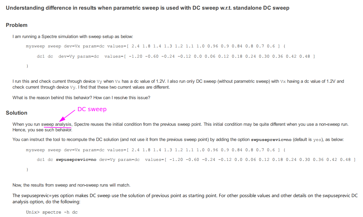
DC sweep & parametric sweep
swpuseprevic
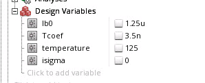
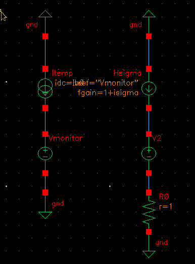
variables with statistical distribution
Specifying Parameter Distributions Using Statistics Blocks
process: generate random number once per MC runmismatch: generate a random number per instance

reference
Article (20498356) Title: How to vary design variables with statistical distribution to be used with Monte Carlo analysis URL: https://support.cadence.com/apex/ArticleAttachmentPortal?id=a1O3w000009ErHHEA0
Spectre Circuit Simulator Reference
DC operating points during TRANSIENT
Andrew Beckettover 11 years ago
Two approaches:
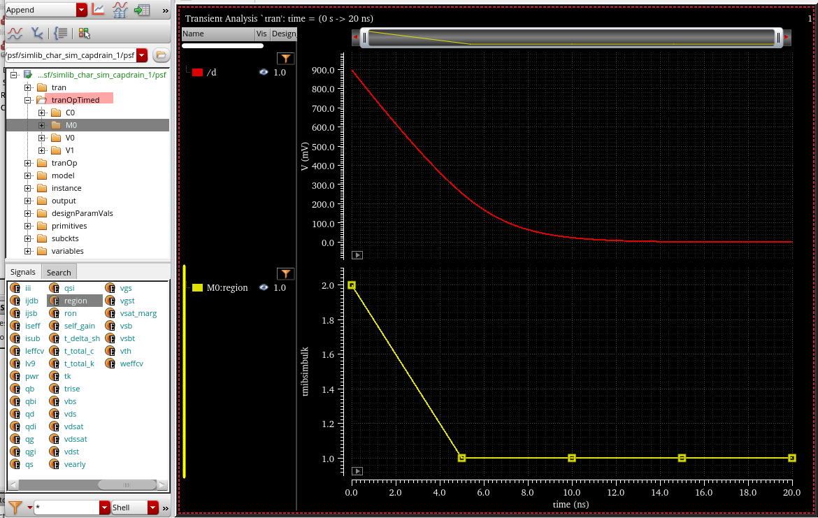
- On the transient options form, there's a field called "infotimes" - specify the times at which you want it to output the dc operating point data. You can then annotate the "transient operating points" from any of these times after the simulation, or access them via the results browser.
- Or you could get the operating point data to be continuously saved during the transient for selected devices - if so, create a file called (say) "save.scs" (make sure it has a ".scs" suffix), and put: save M1:oppoint or save M*:oppoint sigtype=dev in this file, and then reference the file via Setup->Model Libraries or as a "definition file" on Setup->Simulation Files. With this approach you can then find the operating point data for the selected devices in the results browser and plot it versus time (be cautious of saving too much though because this can generate a lot of data if you're not careful)
Regards,
Andrew.
transient options form
setup
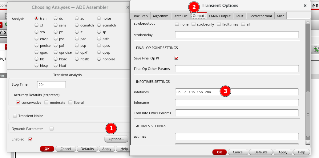
access 1
right-click \(\to\) Annotate \(\to\) Transient Operating Points
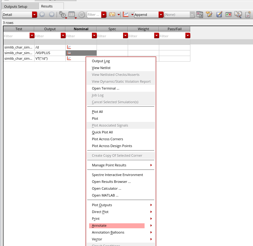
access 2
tranOpTimed
save.scs
1 | save M0:oppoint |
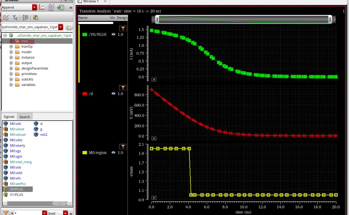
How to Save Node in DSPF?
DSPF Semantics
*|DIVIDER <divider>
<divider> represents the hierarchical pathname
divider. The default hierarchical character is forward slash
(/).
*|DELIMITER <delimiter>
<delimiter>represents the delimiter character used to concatenate an instance name and pin name to form an instance pin name.- It is also represents the delimiter character used to concatenate a net name and subnode number to form a subnode name. The default character is colon (:)
*|BUSBIT <left_busbit_char><right_busbit_char>
<left_busbit_char> and
<right_busbit_char> are used at the end of an
identifier of an array to select a single object of the array.
Objects which may be indexed include nets, primary pins, and instance pins
*|NET <netName> <netCap>
<netName>represents the name of a net. It can be a user-provided net name, the name of the driving pin, or the name of the driving instance pin.<netCap>represents the total capacitance value in farads associated with the net. This may be comprised of capacitances to ground and capacitances to nearby wires.
*|P <pinName> <pinType> <pinCap> {<coord>}
<pinName>represents the name of the pin.<pinType>represents the type of the pin. It can be any of the following: I (Input), O (Output), B (Bidirectional), X (don’t care), S (Switch), and J (Jumper).<pinCap>represents the capacitance value associated with the pin.<coord>is optional. It represents the location of the pin. Multiple pin locations are allowed.
*|S <subNodeName> {<coord>}
subnodes in the net
<subNodeName>represents the name of the subnode. A subnode name is obtained by concatenating the net name and a subnode number using the delimiter specified in the DELIMITER statement. The default delimiter is colon (:).<coord>represents the location of the subnode.
*|I <instPinName> <instName> <pinName> <pinType><pinCap> {<coord>?}
describes instance pins in the net
<instPinName>represents the name of the instance pin. An instance pin name is obtained by concatenating the<instName>and the<pinName>with a delimiting character which is specified by the DELIMITER statement<instName>represents the name of the instance
*|DeviceFingerDelim "@"
MOS finger delimiter
For example, M8's finger is 4, then split into 4 Devices
in DSPF
MM8,MM8@2,MM8@3,MM8@4
its drain terminal will be
MM8:d,MM8@2:d,MM8@3:d,MM8@4:d
DSPF Syntax
DSPF has two sections:
a net section
The net section consists of a series of net description blocks. Each net description block corresponds to a net in the physical design. A net description block begins with a net statement followed by pins, instance pins, subnodes, and parasitic resistor/capacitor (
R/C) components that characterize the electrical behavior of the net.an instance section
The instance section consists of a series of SPICE instance statements. SPICE instance statements begin with an
X.
Each file consists of hierarchical cells and interconnects only.
The DSPF format is as generic and as much like SPICE as possible. While native SPICE statements describe the R/C sections, some non-native SPICE statements complete the net descriptions. These non-native SPICE statements start with the notation "*|" to differentiate them from native SPICE statements. For native SPICE statements, a continuation line begins with the conventional "+" sign in the first column.
The native SPICE statements used by the DSPF format are listed below:
.SUBCKTrepresents a subcircuit statement..ENDSrepresents the end of a subcircuit statement.Rrepresents a resistor element.Crepresents a capacitor element.Erepresents a voltage-controlled voltage sources element.Xrepresents an instance of a cell;*represents a comment line unless it is*|or*+..ENDis an optional statement that represents the end of a simulation session
spectre netlist
hier_delimiter="."
Used to set hierarchical delimiter. Length of
hier_delimiter should not be longer than 1, except the
leader escape character
spfbusdelim = busdelim_schematic [busdelim_parasitic]
This option maps the bus delimiter between schematic netlist and parasitic file (i.e. DSPF, SPEF, or DPF). The option defines the bus delimiter in the schematic netlist, and optionally the bus delimiter in the parasitic file. By default, the bus delimiter of the parasitic file is taken from the parasitic file header (i.e. |BUSBIT [], |BUS_BIT [], or *|BUS_DELIMITER []). If the bus delimiter is not defined in the parasitic file header, you need to specify it by using the spfbusdelim option in schematic netlist.
Exampel
- spfbusdelim=<> - A<1> in the schematic netlist is mapped to A_1 in the DSPF file, if the bus delimiter header in the DSPF file is "_".
- spfbusdelim=@ [] - A@1 in the schematic netlist is mapped to to A[1] in the DSPF file (the bus delimiter in DSPF header will be ignored).
How to Save Net voltage in DSPF
!!! follow the name of net section in DSPF - prepend to top-level devices in the schematic with
X
Assume node n1...n4 are named as below in DSPF file (prefix
X)
n1
XXosc/zip:1
n2
XXosc/zip:2
n3
XXosc/zip:3
n4
XXosc/zip:4
To save these nodes, you can add follow code in Definition Files
saveopt.scs
1 | save Xwrapper.Xvco.XXosc\/zip\:1 |
Escape character
\is used for hierarchical pathname divider/and subnode:By the way,
.is hierarchical delimiter of SpectreCalibre always prepend one X to instance name of schematic in generated DSPF file
The DSPF design is flatten, the DIVIDER character indicate the hierarchy
1 | save Xwrapper.Xvco.XXosc\/zip |
The above save voltage, however I'm NOT sure which node it save.
To avoid this unsure problem, the MOS terminal may be better choice to save.
But keep in mind
- OD resistance is lumped in the FEOL model
- M0OD and above layer resistances are extracted by RC tool
How to Save Current in DSPF
!!! follow the name of instance section of DSPF - prepend to top-level devices in the schematic with
XX
MOS in schematic: Xsupply.M4
MOS related information in DSPF (prefix XX in instance
section):
1 | ... |
To save drain current:
1 | save Xvco.XXXsupply\/MM4:d |
<instName>in*|I <instPinName> <instName> <pinName> <pinType><pinCap> {<coord>?}which has prefixXcorresponding to schematic is NOT the instance name in DSPF. The instance name is in instance section and has prefixXX
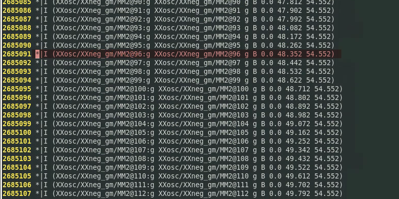
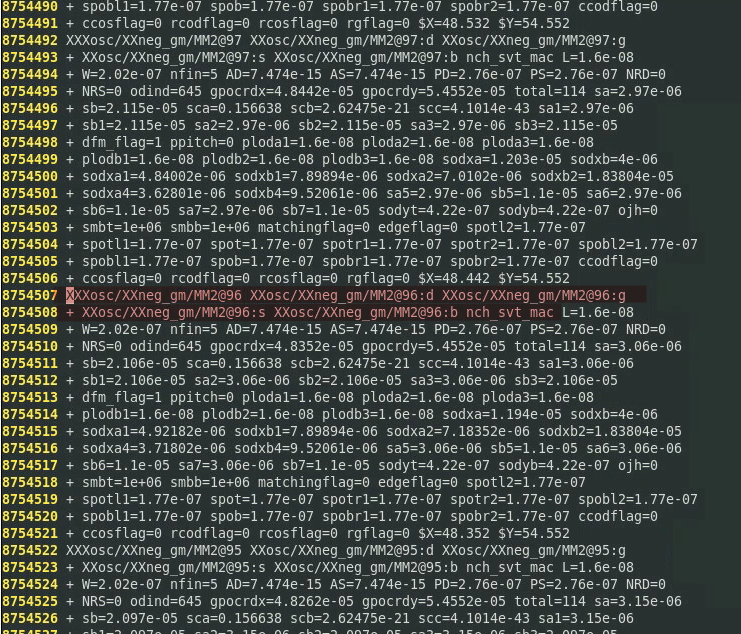
!!! Only work for MOS terminal current. Fail to apply to block pin
Thinking about voltage and current save
- MOS device always prepend with
M - To save net voltage, take account of the prefix
Xof top-level device - To save MOS terminal, take account of the prefix
XXof top-level device
Post-layout netlists are created by layout extraction tools - Mentor Calibre
Differences Between DSPF and Schematic Names
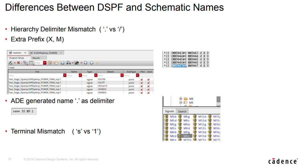
- MOS Terminal Mismatch ( ‘s’ vs ‘1’)
- Schematic: number '1' ,'2', '3','4'
- DSPF: 'd', 'g', 's','b'
.simrc file
If DSPF files show such differences, you can set options in the .simrc file to update the save statement in the netlist so that the device names match with those in the DSPF file
Additionally, dspf_include reads all the DSPF lines
starting with * (|NET, |I, *|P,*|S), while
include considers all related lines as comments.
Only verified to DSPF output of Mentor Calibre
1 | ; ensure that the netlist is recreated each time |
spfFileDevicePrefixForTermCurrentandspfFileDevicePrefixForOppointsare applicable to MOS devices only.
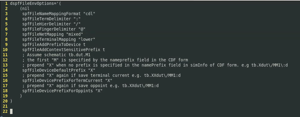
Both
@and__have been observed as Finger Delimiter in single DSPF . wired...
signal name saved using wildcard operator
How to find the signal name saved using wildcard operator with save statement in spectre?
method 1
From ADE L or ADE XL Test Editor, you can use menu Simulation →
Options → Analog→ Miscellaneous → Addition arguments
field:dump_wildcard_info=yes
method 2
add below in netlist file or Simulation Files → Definition
Files:saveopt.scs
saveopt.scs
1 | wcOption options dump_wildcard_info=yes |
saved file
After running simulation, saved wildcard summary is save into file
<netlist_file_name>.wildcard.out*
1 | Wildcard match summary: |
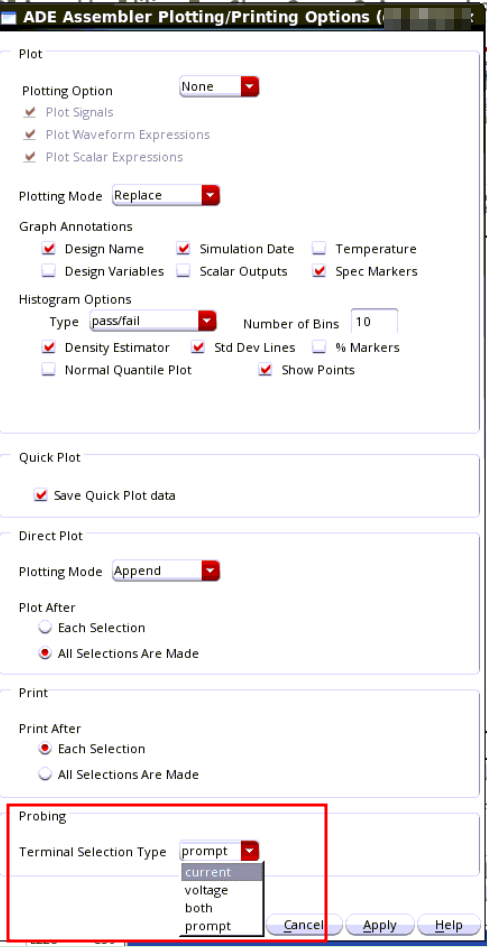
Save and Plot terminal voltage in ADE Explorer and Assembler
.cdsinit
1 | envSetVal("auCore.selection" "terminalSelectionType" 'cyclic "current") |
Available options are current, voltage, both or prompt and the default is current which matches the default behavior in previous releases.
- The schematic will have an ellipse annotation where a current probe has been saved,
- a V annotation for a voltage probe,
- and both annotations for both.
NOTE: Starting with IC 6.1.8 ISR5, you can now set this from Options->Plotting/Printing
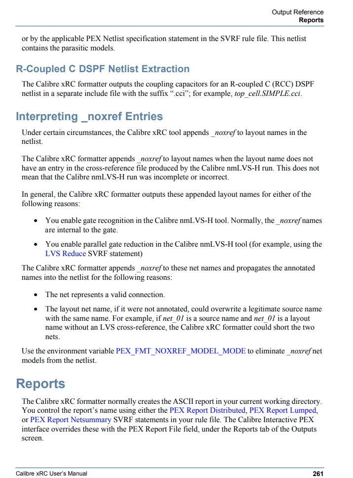
Interpreting _noxref Entries
You enable gate recognition in the Calibre nmLVS-H tool. Normally, the _noxref names are internal to the gate

Saving net with hierarchy delimiter and colon (:) in net name gives WARNING (SPECTRE-8282) during simulation
Problem
I am running simulation using an spf/spef file which has a net name definition as shown in the below example:
1 | // input.scs |
The net name is x1/x1:DRN. During the simulation, the following warning is reported:
Warning from spectre during initial setup.
1 | WARNING (SPECTRE-8282): `xpi1.x1/x1' is not a device or subcircuit instance name. |
How can I save this net for plotting and measurements?
Solution
The colon (:) in the save statement specifies terminal current. So, the save statement used above is for terminal current and, hence, the warning messages are reported.
1 | save xpi1.x1\/x1:DRN |
You need to modify the save statement as below:
1 | save xpi1.x1\/x1\:DRN |
Now, run the simulation and the issue will be resolved.
DSPF r vs rcc
rcc

c

only c dspf give the lumped capacitance
EMIR via Voltus-Fi
general terminology
DC related
Imax in T*'s DRC document is the maximum allowed DC current, which depends on Length and Width only
Iavg is the average value of the current, which is the effective DC current. Therefore, Iavg rules are identical to Imax rules \[ I_{\text{avg}}=\frac{\int_0^\tau I(t)dt}{\tau} \] Similarly, Iabsavg rules are identical to Imax rules, too \[ I_{\text{AbsAvg}}=\frac{\int_0^\tau |I(t)|dt}{\tau} \]
rms
Irms is the root-mean-square of the current through a metal line, which depends w(in um), the drawn width of the metal line and \(\Delta T\), the temperature rise due to Joule heating. \[ I_{\text{rms}}=\left[\frac{\int_0^\tau I(t)^2dt}{\tau} \right]^{1/2} \]
peak current
Ipeak in T*'s DRC document is the current at which a
metal line undergoes excessive Joule heating and can begin to melt.
Ipeak is corresponding to
EM Current Analysis: max in Voltus-Fi Analysis Setup \[
I_{\text{peak}}=\max(|I(t)|)
\] The limit for the peak current is \[
I_{\text{peak,limit}}=\frac{I_{\text{peak\_DC}}}{\sqrt{r
} }
\] where r is the duty ratio
The relationship between Ipeak and Ipeak_DC is merged in DRC document so that there is only Ipeak equation in document
\(I_{\text{peak,limit}}\) depends on \(t_D\), r, width and length
\[ r=\frac{t_D}{\tau} \]
where \(t_D\) is equivalent duration
\[
t_D =\frac{\int_0^\tau |I(t)|dt}{I_{\text{peak}}}
\] or \[
r=\frac{I_{\text{AbsAvg}}}{I_{\text{peak}}}
\] 
where the drawn width is 1um, r is 0.1

 \[
9.37*(1-0.004)/\sqrt0.1 = 29.512
\]
acpeak/pwc
It's same with max EM Current Analysis in Voltus-Fi
dynamicACPeak

This option affect how duty ratio r is computed in max
and acpeak/pwc EM current Analysis
When the dynamicACPeak variable is set to
true or multiPeak \[
r=\frac{T_d}{T_{\text{total}}}
\]
where \(T_{\text{total}} = \text{EMIR time window}\)
\(T_d\) = the time duration in
microsecond of the total "On Time" period based on IPWC
Pulse-Wise Constant EM current calculation (IPWC)
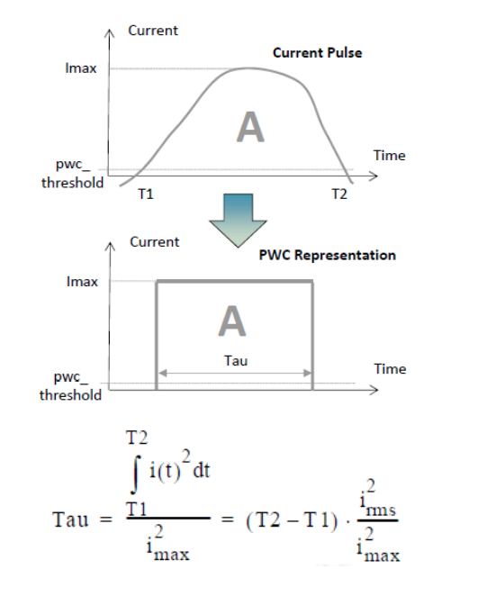
where Tau is \(T_d\) in above formula
!!! It seems that t*'s PDK don't support
dynamicACPeak=true
IR drop filter layers
EM techfile (qrcTechFile) may take diffusion contact (n_odtap, p_odtap in DSPF file) into account during IR drop analysis. And these segment often dominate IR drop, but we as IC designer can NOT improve them. In general, the IR drop to M1 layer is enough and feasible.
Regular analysis statements in emir configuration
1 | net name=[I0.vdd I0.vss] analysis=[vmax vavg] |
emirreport command
Creating reports for specific nets after simulation using
emirreport
Create a new config file as shown below:
1 | ** test.conf** |
Run emirreport on the command line using the
emirdatabase (emir*.bin) and test.conf
created above in
1 | % emirreport -64 -c test.conf -db <emirdatabase> -outdir newreport |
database
simulation result
input.emir0_bin: The first EMIR Analysis which is DC or Transient, which depends on Analyses order
input_tran.emir0_bin: EMIR Analysis in Transient simulation
input_dcOp.emir0_bin: EMIR Analysis in DC simulation
For example
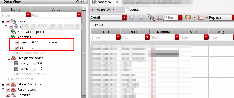
Two results are generated input.emir0_bin and
input_dcOp.emir0_bin and their reports respectly


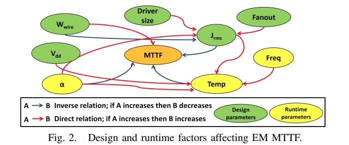
Fix Electromigration
| Type | wider wire | downsize drivers | decrease fanout |
|---|---|---|---|
| RJ JMAX | ✓ | ✓ | |
| JAVG | |||
| JABSAVG | |||
| JACPEAK | |||
| JACRMS | ✓ | ✓ | ✓ |
Iavg
The average value of the current, which is the effective DC current
Irms
Irms rule relates to the heat or Joule-heating of metal lines
Ipeak
The main goal of the Ipeak limits is to ensure that no thermal breakdown could occur on single overshoot events. If the signal may not have a high current density but if it has a very large peak current density, then, local melting will happen and cause failures
QA
Q. Why “length” column in EM results form doesn’t show extracted length, it shows “NA”.
A. Voltus-Fi reports the “length” column only when length rules are present in the emDataFile.
Seeing different port currents with and without emir simulations for same dspf included in EMIR Direct method using dspf_include.
Split Pins (*|P) in DSPF are only shorted in the EMIR flow not in the regular spectre flow. Islands patching is only performed in EMIR only
Setting temperature for EM analysis
By Default, Voltus-FI and VPS pick up the current density limit for temperature at which simulation has been performed.
By the way,
Design Variables- temperature will override the temperature in Setup toolbar which is gray in ADE Explorer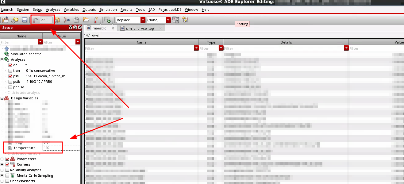
AC Peak EM analysis - Voltus-Fi
The available options within the EM current analysis section in the EMIR Analysis Setup form are:
max / avg / avgabs / rms.In order to enable the AC Peak based information when loading the EM results, both max and avg should be selected when setting up the EMIR Analysis Setup.
With this configuration, the AC Peak option becomes available and can be used.
How to print average, rms, and peak current of device tap in Spectre/Voltus FI EMIR analysis
The following option enables you to save the average, rms, and peak tap currents in the emir0bin file and report it in the input.rpt_tapi file.
1
solver report_tapi=true
Add this option in emir.conf to enable the reporting of tap current after the Spectre EMIR simulation. The input.rpt_tapi file will be saved in the psf/raw directory.
Note: This feature is supported in SPECTRE20.1 ISR14 and later versions.
emir.conf file
emir.conffile is generated automaticaly after configure EM/IR Analysis in ADE, which is in netlist directory.
Setting default path for EM rules file in APS EMIR analysis
set the following environment variable in your terminal
1
setenv EMDATAFILE < path to EM rules file>
or set in
.cdsinit1
setShellEnvVar("EMDATAFILE=<path to EM rules file>")
Print node names and length associated with parasitic resistors in EM report file
export CDS_MMSIM_VOLTUSFI_ROOT=$CDSHOMEPrinting the parasitic resistor length in the EM report
1
emirutil reportLength=true
Printing nodes that are associated with the parasitic resistor
1
emirutil reportNodeName=true
Once these are enabled, you will have the Length, Node_1, and Node_2 columns printed in the EM report file, as shown below:

Is it possible to run RMS IR Drop analysis using Voltus-Fi?
Typically, in a simulation, Power/Ground nets are always biased with a constant DC source. Hence, at present, Voltus-Fi only supports Average and Maximum (Peak) IR Drop analysis.
For a net to have data for IR analysis(vmax/vavg), the net/node must be connected to a DC vsource or a vsource which is constant within the emir time window.
Can we change the time window of EM computation after the simulation completed ?
It is not possible to modify the EM time window without re-running the full simulation.
However you can specify several time window in the emir conf file for instance for 2 time window [0 to 10n] and [10n 20n]
1
time window=[0 10n 10n 20n]
In that case it will create 2 emir_bin files and then 2 different em report files according to the 2 different time windows.
How to print segment_W values being used to compute EM limits
You can use the following option to print
segment_Wto the report:1
emirutil reportSegmentWidth=[true]
This would print a
Segment_wcolumn in the report containing the segment width values used for computing the limit:Pass/Fail % Resistor layer Current Width PathLength I limit X1 Y1 X2 Y2 J/JMAX Res ViaArea No of needed vias width/#via J limit Segment_w (mA) (um) (um) (um) (um) (um) (um) (nm^2) (um/#) (A/um) pass-100.0 Rj3292 Met1 9.02376e-12 0.1 42.72 1.10067 0.350 11.568 0.350 11.376 8.19843e-12 0.7382 NA NA 0.0001 0.0110067 0.1 pathLength vs Length in EM report file
Length: parasitic resistor length, which is set by
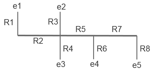
emirutil reportLength=truepathlength: Blech length is also known as "Short length" or "Path length", and can be explained as : The longest and continuous centerline path from edge to edge among the connected wire shapes on the same metal layer.
- For all resistors falling on this shape, same pathLength is reported.
- After the longest path in shape has been determined the tool applies the same blech length to all the resistor falling on that shape.
- This resistor length is NOT used in EM analysis because EM rules consider Blech length of the resistor.

where W is the wire width and L is the Blech length.
By default the tool will sum all branches of a given metal layer. In other words the path length that will be used to look up the EM density limit is :
Bl = $l(R1) + $l(R2) + $l(R3) + $l(R4) + $l(R5) + $l(R6) + $l(R7) + $l(R8)
How to enable EMIR analysis in PSS simualtion ?
To enable EMIR in PSS, you have to enable DC and/or Tran simulation simultaneously. Two or more binary results file should be generated and select the file based file name or configure text file in
psfdirectory.(given ICADVM 18.1 ISR11, Spectre 19.1 ISR6)
reference
AC Peak Analysis Using IPWC Rapid Adoption Kit (RAK) Product Version: IC6.1.8 ISR10, SPECTRE19.1 ISR5 April 2020
Posser, Gracieli & Sapatnekar, Sachin & Reis, Ricardo. (2017). Electromigration Inside Logic Cells. 10.1007/978-3-319-48899-8.
A. B. Kahng, S. Nath and T. S. Rosing, "On potential design impacts of electromigration awareness," 2013 18th Asia and South Pacific Design Automation Conference (ASP-DAC), 2013, pp. 527-532, doi: 10.1109/ASPDAC.2013.6509650.
Kumar, Neeraj and Mohammad S. Hashmi. “Study, analysis and modeling of electromigration in SRAMs.” (2014).
N. S. Nagaraj, F. Cano, H. Haznedar and D. Young, "A practical approach to static signal electromigration analysis," Proceedings 1998 Design and Automation Conference. 35th DAC. (Cat. No.98CH36175), 1998, pp. 572-577, doi: 10.1109/DAC.1998.724536.
Blaauw, David & Oh, Chanhee & Zolotov, Vladimir & Dasgupta, Aurobindo. (2003). Static electromigration analysis for on-chip signal interconnects. Computer-Aided Design of Integrated Circuits and Systems, IEEE Transactions on. 22. 39 - 48. 10.1109/TCAD.2002.805728.