Bias Circuit
replica biasing
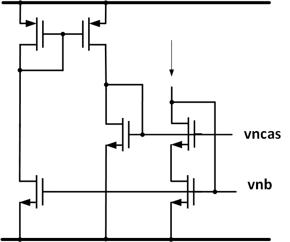
TODO 📅
current mirror with source follower

source follower alleviate gate leakage impact on reference current
constant-gm
aka. Beta-multiplier reference
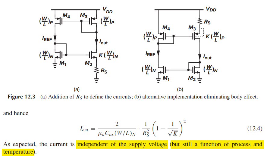
\(I_\text{out}\) is PTAT in case temperature coefficient of \(R_s\) is less than that of \(\mu_n\)
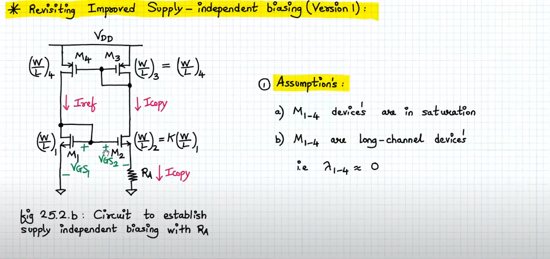
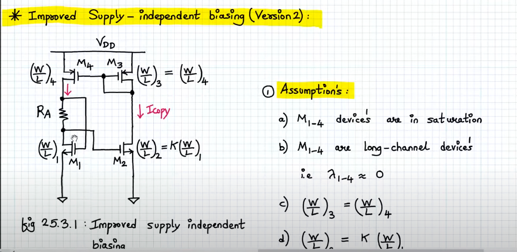
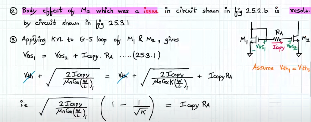
Body effect of M2

Boris Murmann, Systematic Design of Analog Circuits Using Pre-Computed Lookup Tables
S. Pavan, "Systematic Development of CMOS Fixed-Transconductance Bias Circuits," in IEEE Transactions on Circuits and Systems II: Express Briefs, vol. 69, no. 5, pp. 2394-2397, May 2022
S. Pavan, "A Fixed Transconductance Bias Circuit for CMOS Analog Integrated Circuits", IEEE International Symposium on Circuits and Systems, ISCAS 2004, Vancouver , May 2004
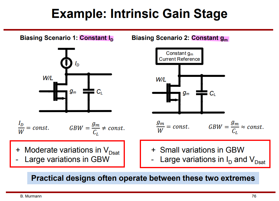
Why MOS in saturation ?
\(g_m\), \(g_\text{ds}\) at fixed \(V_\text{GS}\)
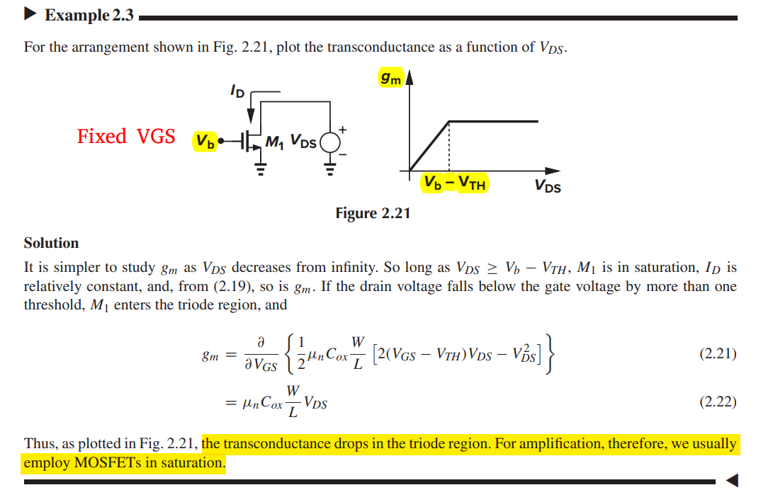
\(g_{ds}\) is constant in saturation region
in triode region \[ g_{ds} = \mu_nC_{ox}\frac{W}{L}(V_{GS}-V_{TH}-V_{DS}) \]
Interestingly, \(g_m\) in the saturation region is equal to the inverse of \(R_\text{on}\) in the deep triode region.

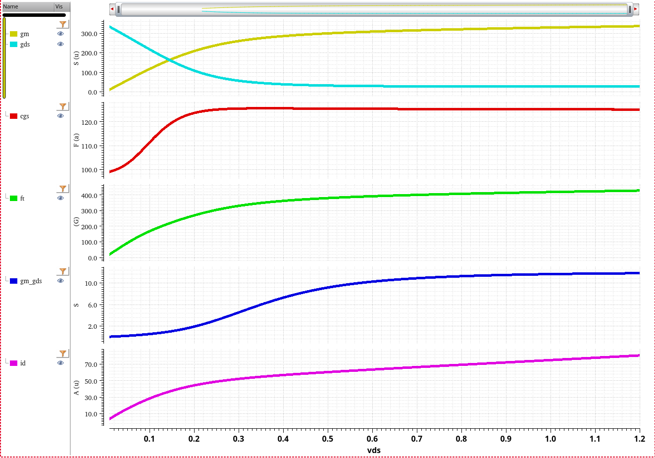
\(g_m\), \(g_\text{ds}\) at fixed \(I_d\), \(V_G\)
In triode region \[ I_D = \frac{1}{2}\mu_nC_{ox}\frac{W}{L}[2(V_{GS}-V_{TH})V_{DS}-V_{DS}^2] \] where \(I_D\) and \(V_G\) is fixed
Then \(V_S\) can be expressed with \(V_D\), that is \[ V_S = V_{GT} - \sqrt{(V_{GT}-V_D)^2+V_{dsat}^2} \] where \(V_{GT}=V_G-V_{TH}\), \(V_{dsat}\) is \(V_{DS}\) saturation voltage \[ g_m = \mu_nC_{ox}\frac{W}{L}\left(V_D-V_{GT}+\sqrt{(V_{GT}-V_D)^2+V_{dsat}^2}\right) \] Then \[ \frac{\partial g_m}{\partial V_D} \propto 1 - \frac{V_{GT}-V_D}{\sqrt{(V_{GT}-V_D)^2+V_{dsat}^2}} \gt 0 \]
That is, \(g_m \propto V_D\)
\[\begin{align} g_{ds} &= \mu_nC_{ox}\frac{W}{L}(V_{GS}-V_{TH}-V_{DS}) \\ &= \mu_nC_{ox}\frac{W}{L}(V_{GT}-V_{D}) \end{align}\]
That is, \(g_{ds} \propto -V_D\)
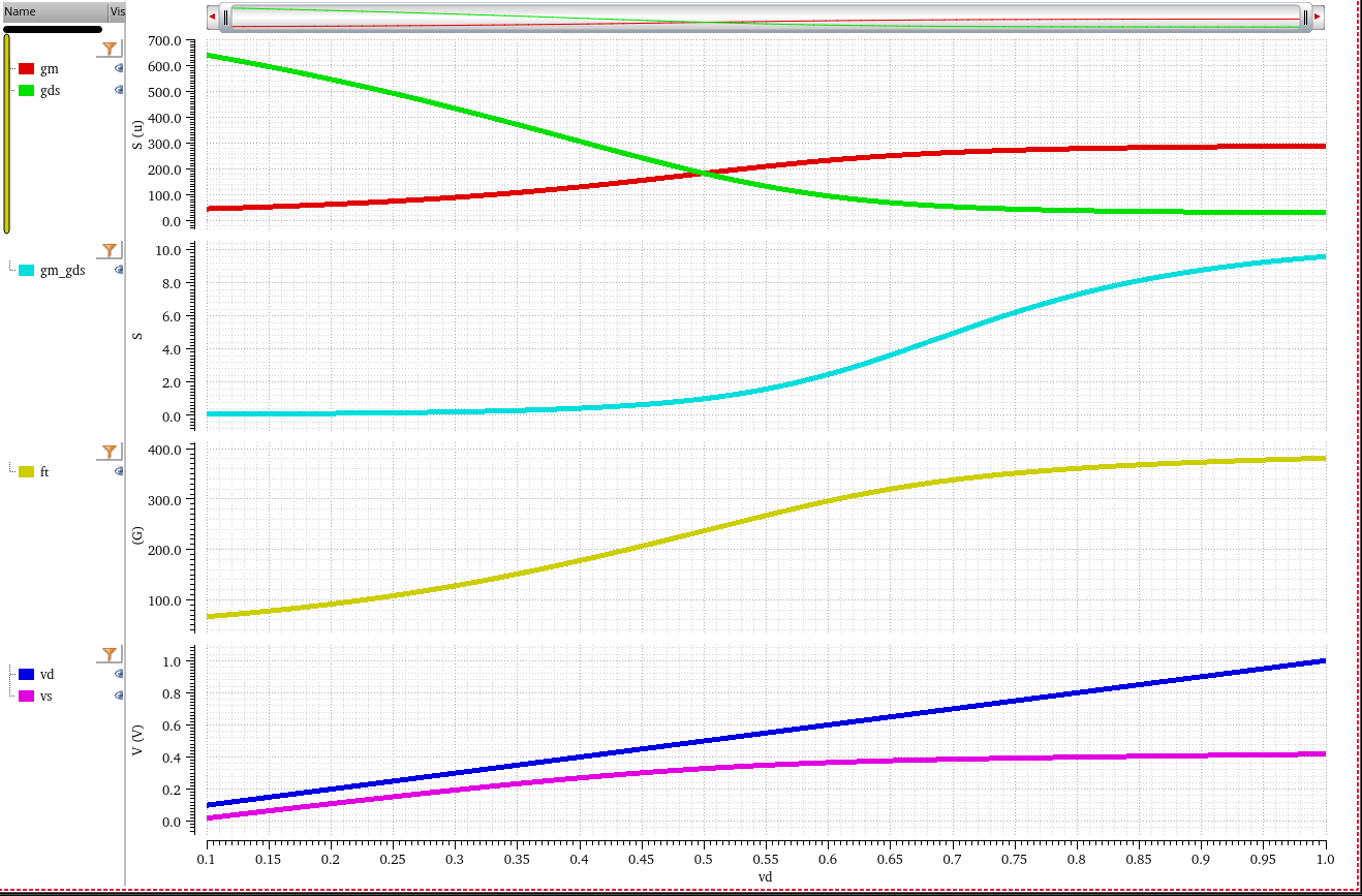
Both gain and speed degrade once entering triode region, though Id is constant
Cascode MOS
The low threshold voltage of cascode MOS don't help decrease the minimum output voltage

Channel-length modulation
❗ There it not channel-length modulation in the triode region
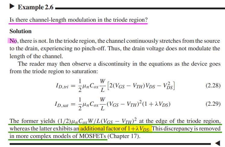
\[\begin{align} I_D &=\frac{1}{2}\mu_nC_{ox}\frac{W}{L}(V_{GS}-V_{TH})^2(1+\frac{\Delta L}{L}) \\ I_D &=\frac{1}{2}\mu_nC_{ox}\frac{W}{L}(V_{GS}-V_{TH})^2(1+\lambda V_{DS}) \\ I_D &=\frac{1}{2}\mu_nC_{ox}\frac{W}{L}(V_{GS}-V_{TH})^2(1+\frac{V_{DS}}{V_A}) \end{align}\]
where \(\frac{\Delta L}{L}=\lambda V_{DS}\) and \(V_A=\frac{1}{\lambda}\)
\(\lambda\) is channel length modulation parameter
\(V_A\), i.e. Early voltage is equal to inverse of channel length modulation parameter
The output resistance \(r_o\)
\[\begin{align} r_o &= \frac{\partial V_{DS}}{\partial I_D} \\ &= \frac{1}{\partial I_D/\partial V_{DS}} \\ &= \frac{1}{\lambda I_D} \\ &= \frac{V_A}{I_D} \end{align}\]
Due to \(\lambda \propto 1/L\), i.e.
\(V_A \propto L\) \[
r_o \propto \frac{L}{I_D}
\] 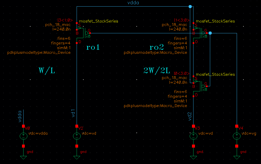
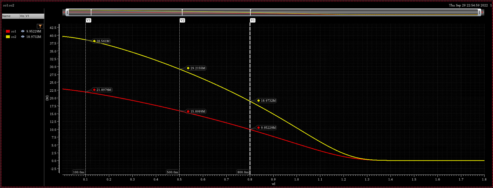
The output resistance is almost doubled using Stacked FET in saturation region
\(V_t\) and mobility \(\mu_{n,p}\) are sensitive to temperature
- \(V_t\) decreases by 2-mV for every 1\(^oC\) rise in temperature
- mobility \(\mu_{n,p}\) decreases with temperature
Overall, increase in temperature results in lower drain currents
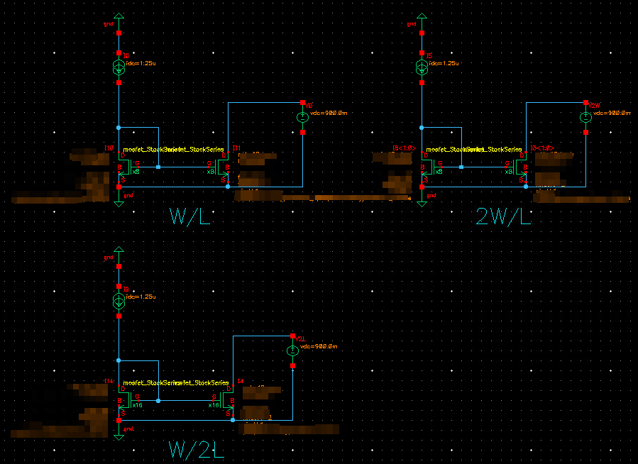
current mirror mismatch
The current mismatch consists of two components.
- The first depends on threshold voltage mismatch and increases as the overdrive \((V_{GS} − V_t)\) is reduced.
- The second is geometry dependent and contributes a fractional current mismatch that is independent of bias point.
\[ \Delta I_D = g_m\cdot \Delta V_{TH}+I_D\cdot \frac{\Delta(W/L)}{W/L} \]
where mismatches in \(\mu_nC_{ox}\) are neglected
\[\begin{align} \Delta V_{TH} &= \frac{A_{VTH}}{\sqrt{WL}} \\ \frac{\Delta(W/L)}{W/L} &= \frac{A_{WL}}{\sqrt{WL}} \end{align}\]
summary:
| Size | \(g_m\) | \(\Delta V_{TH}\) | \(\frac{\Delta(W/L)}{W/L}\) | mismatch (%) | simu (%) |
|---|---|---|---|---|---|
| W, L | 1 | 1 | 1 | \(I_{\Delta_{V_{TH}}}+I_{\Delta_{WL}}\) | 3.44 |
| W, 2L | \(1/\sqrt{2}\) | \(1/\sqrt{2}\) | \(1/\sqrt{2}\) | \(I_{\Delta_{V_{TH}}}/2+I_{\Delta_{WL}}/\sqrt{2}\) | 1.98 |
| 2W, L | \(\sqrt{2}\) | \(1/\sqrt{2}\) | \(1/\sqrt{2}\) | \(I_{\Delta_{V_{TH}}}+I_{\Delta_{WL}}/\sqrt{2}\) | 2.93 |
| We get \(I_{\Delta_{V_{TH}}}\simeq 1.71\%\) and \(I_{\Delta_{WL}} \simeq 1.73\%\) |
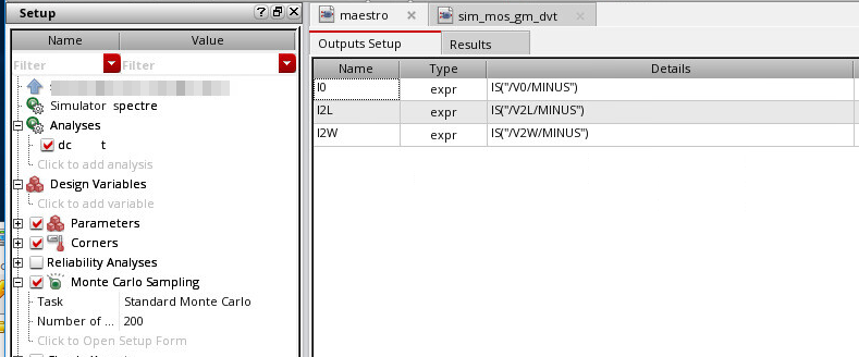
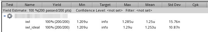
Biasing current source and global variation Monte Carlo
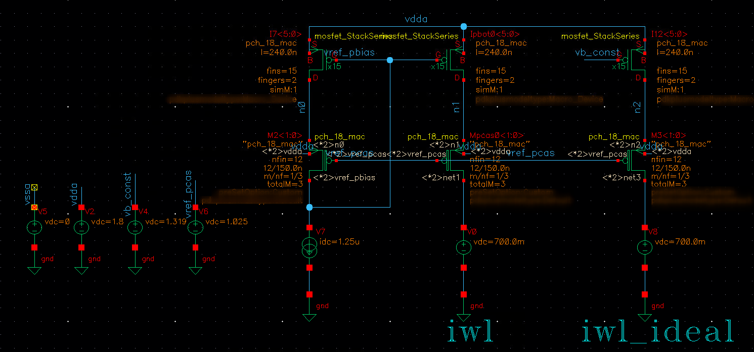

iwl: biased by mirror
iwl_ideal: biased by vdc source, whose value is typical corner
For local variation, constant voltage bias (vb_const in schematic) help reduce variation from \(\sqrt{2}\Delta V_{th}\) to \(\Delta V_{th}\)
For global variation, all device have same variation, mirror help reduce variation by sharing same \(V_{gs}\)
- global variation + local variation (All MC)
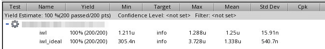
- local variation (Mismatch MC)
- global variation (Process MC)
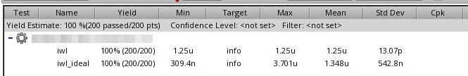
We had better bias mos gate with mirror rather than the vdc source while simulating sub-block.
This is real situation due to current source are always biased by mirror and vdc biasing don't give the right result in global variation Monte Carlo simulation (542.8n is too pessimistic, 13.07p is right result)
Small gain theorem
Dr. Degang Chen, EE 501: CMOS Analog Integrated Circuit Design [https://class.ece.iastate.edu/djchen/ee501/2020/References.ppt]
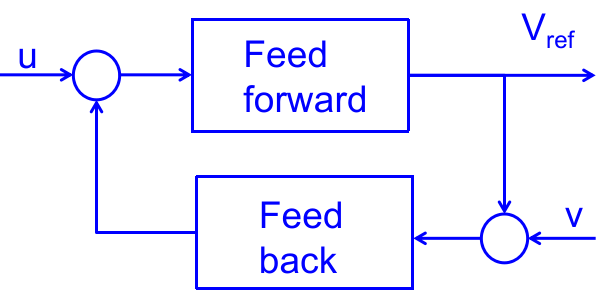
For any given constant values of u and v, the constant values of variables that solve the the feed back relationship are called the operating points, or equilibrium points.
Operating points can be either stable or unstable.
An operating point is unstable if any or some small perturbation near it causes divergence away from that operating point.
If the loop gain evaluated at an operating point is less than one, that operating point is stable.
This is a sufficient condition
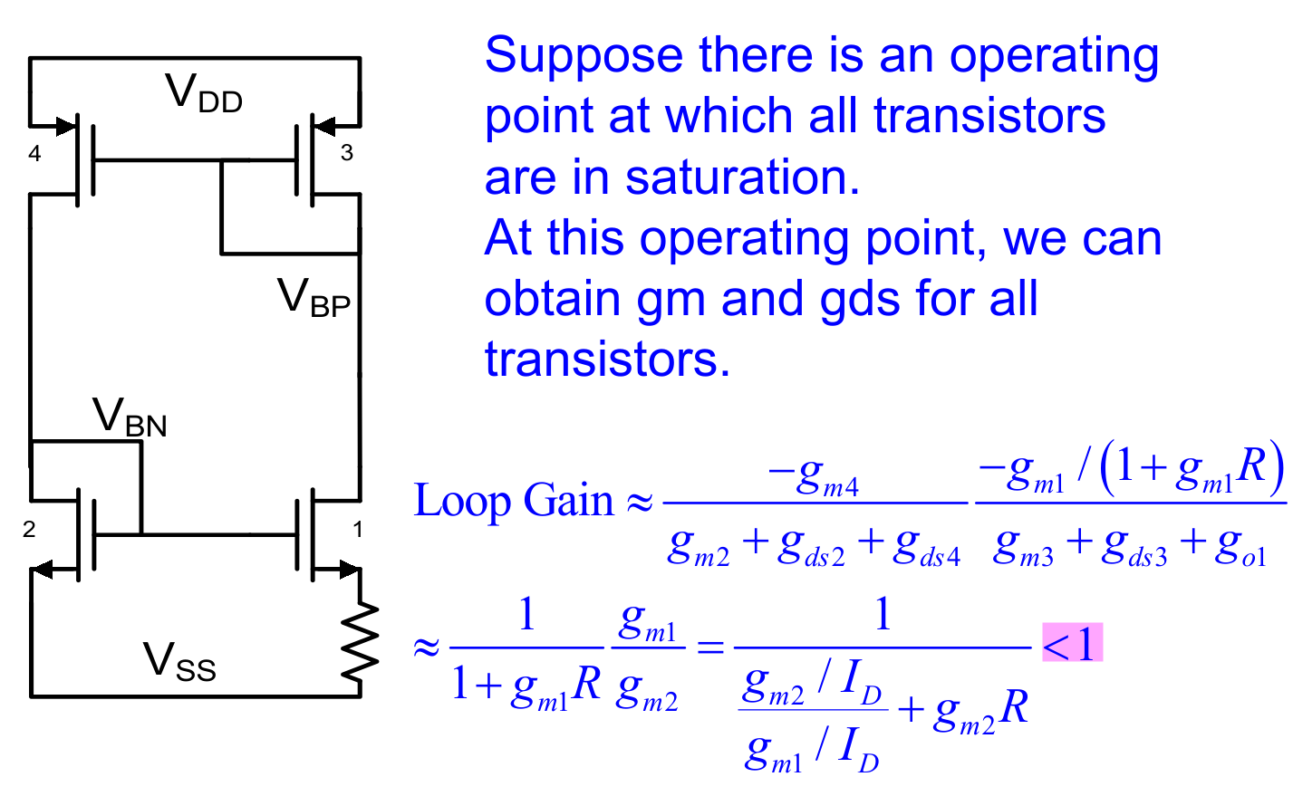
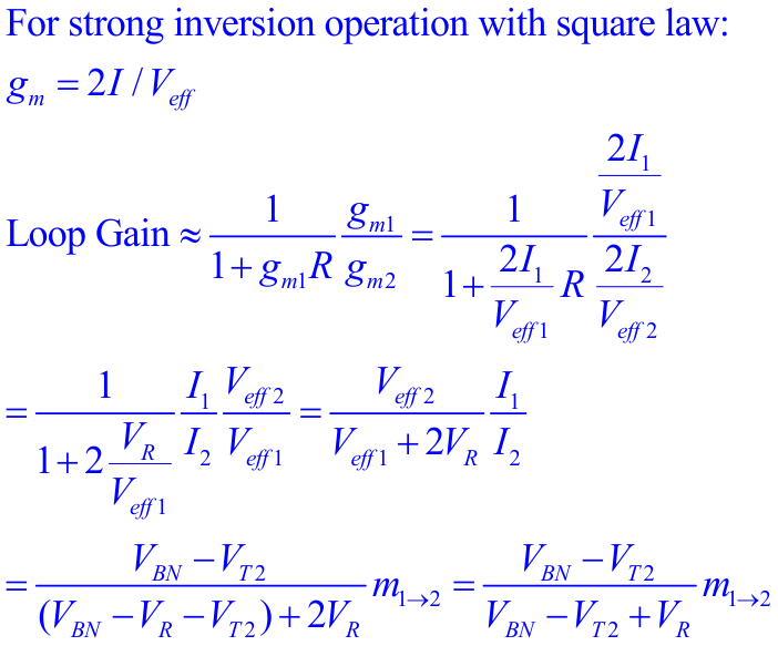
With \(m_{1\to 2} = 1\) \[ \text{Loop Gain} \simeq \frac{V_{BN}-V_{T2}}{V_{BN}-V_{T2} + V_R} \tag{$LG_0$} \] Assuming all MOS in strong inv operation, \(I\), \(V_{BN}\) and \(V_R\) is obtain \[\begin{align} I &= \frac{2\beta _1 + 2\beta _2 - 4\sqrt{\beta _1 \beta _2}}{R^2\beta _1 \beta _2} \\ V_{BN} &= V_{T2} + \frac{2}{R\beta _2}(1- \sqrt{\frac{\beta _2}{\beta _1}}) \\ IR &= \frac{2}{R}\left( \frac{1}{\sqrt{\beta_2}} - \frac{1}{\sqrt{\beta_1}} \right) \end{align}\]
Substitute \(V_{BN}\) and \(V_R\) of \(LG_0\) \[\begin{align} \text{Loop Gain} & \simeq \frac{1-\sqrt{\frac{\beta_2}{\beta_1}}}{\frac{\beta_2}{\beta_1} - 3\sqrt{\frac{\beta_2}{\beta_1}}+2} \\ &= \frac{1}{2-\sqrt{\frac{\beta_2}{\beta_1}}} \tag{$LG_1$} \end{align}\]
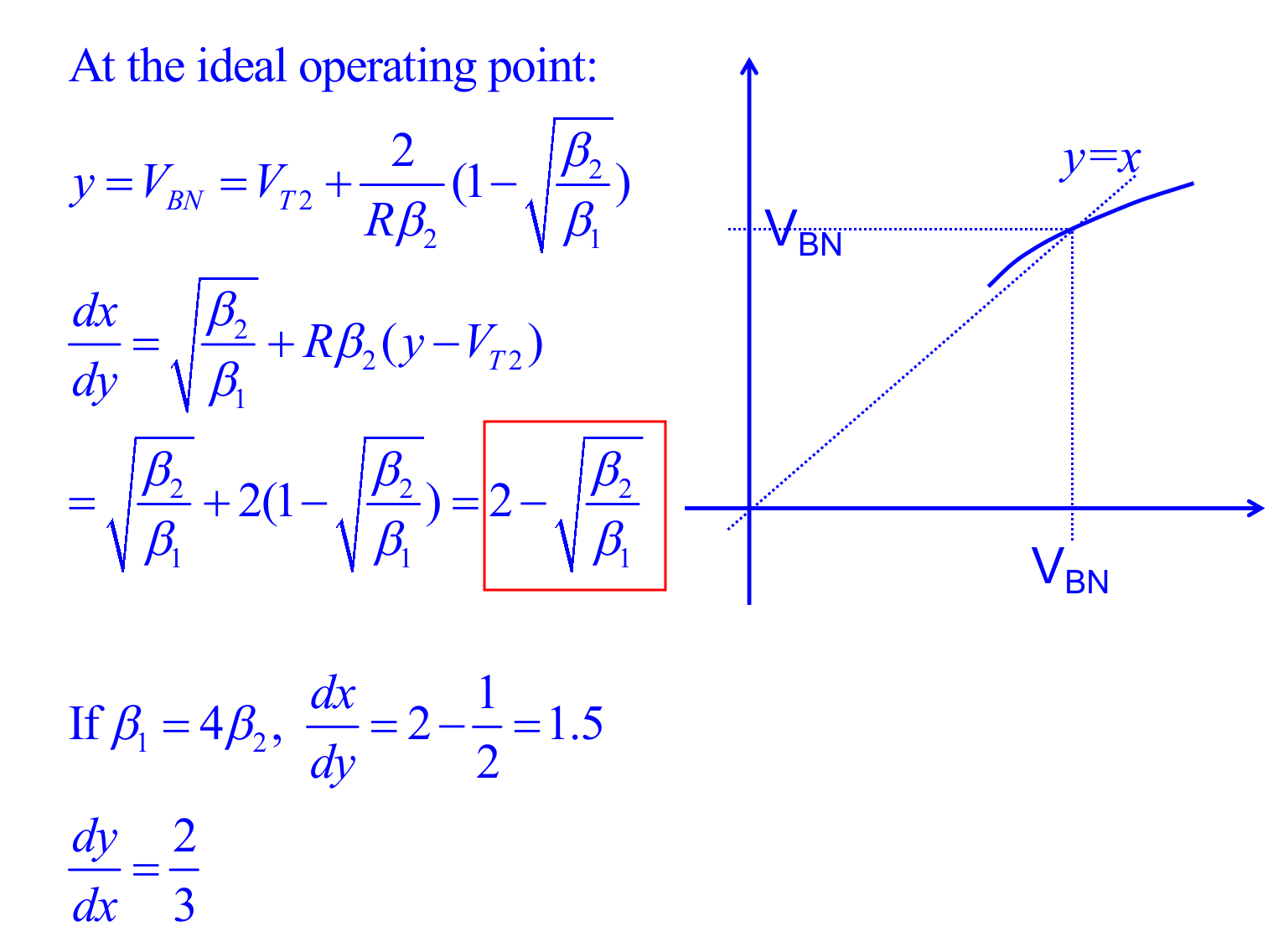
Alternative approach for Loop Gain
using derivation of large signal
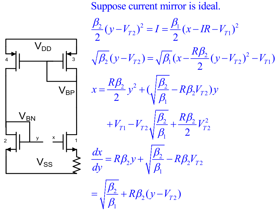
❗❗❗ R should not be on the other side
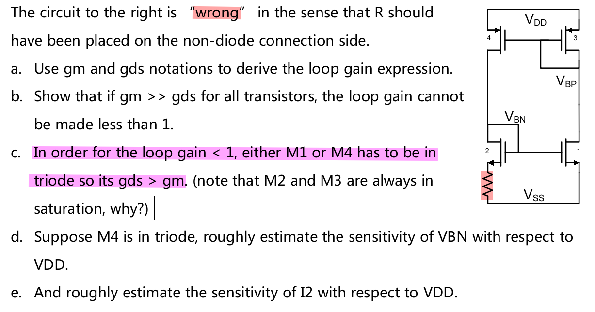
Self-Biasing Cascode


reference
B. Razavi, "The Design of a Low-Voltage Bandgap Reference [The Analog Mind]," in IEEE Solid-State Circuits Magazine, vol. 13, no. 3, pp. 6-16, Summer 2021, [https://www.seas.ucla.edu/brweb/papers/Journals/BR_SSCM_3_2021.pdf]
Shanthi Pavan, IIT Madras, India , ISSCC 2026: Circuit Insights Voltage and Current Reference Generation [https://youtu.be/i1bKJvtiXmY], [slides]