Successive Approximation (SAR) ADC
Reference Ripple
C-H Chan (U. of Macau) "Extreme SAR ADCs - Exploring New Frontiers" Online Course (2024) : Reference Buffer in SAR ADC [https://youtu.be/vj98B7AaC9E]
C. Li, C. -H. Chan, Y. Zhu and R. P. Martins, "Analysis of Reference Error in High-Speed SAR ADCs With Capacitive DAC," in IEEE Transactions on Circuits and Systems I: Regular Papers, vol. 66, no. 1, pp. 82-93, Jan. 2019 [https://ime.um.edu.mo/wp-content/uploads/magazines/961546494e705f6fd16b9f785a121030.pdf]
J. Zhong, Y. Zhu, S. -W. Sin, S. -P. U and R. P. Martins, "Thermal and Reference Noise Analysis of Time-Interleaving SAR and Partial-Interleaving Pipelined-SAR ADCs," in IEEE Transactions on Circuits and Systems I: Regular Papers, vol. 62, no. 9, pp. 2196-2206, Sept. 2015 [https://sci-hub.st/10.1109/TCSI.2015.2452331]
C. -H. Chan et al., "60-dB SNDR 100-MS/s SAR ADCs With Threshold Reconfigurable Reference Error Calibration," in IEEE Journal of Solid-State Circuits, vol. 52, no. 10, pp. 2576-2588, Oct. 2017 [https://ime.um.edu.mo/wp-content/uploads/magazines/407e580ac0218605bcf9b9bbd0ea1109.pdf]
TODO 📅
sample-by-sample
3rd harmonic

bit-by-bit
The amplitude of the reference ripple is code-dependent as it is correlated with switching energy in each bit cycling
SAR ADC Noise Analysis
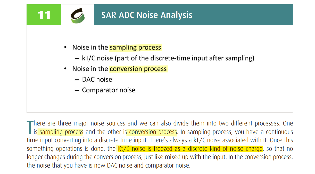
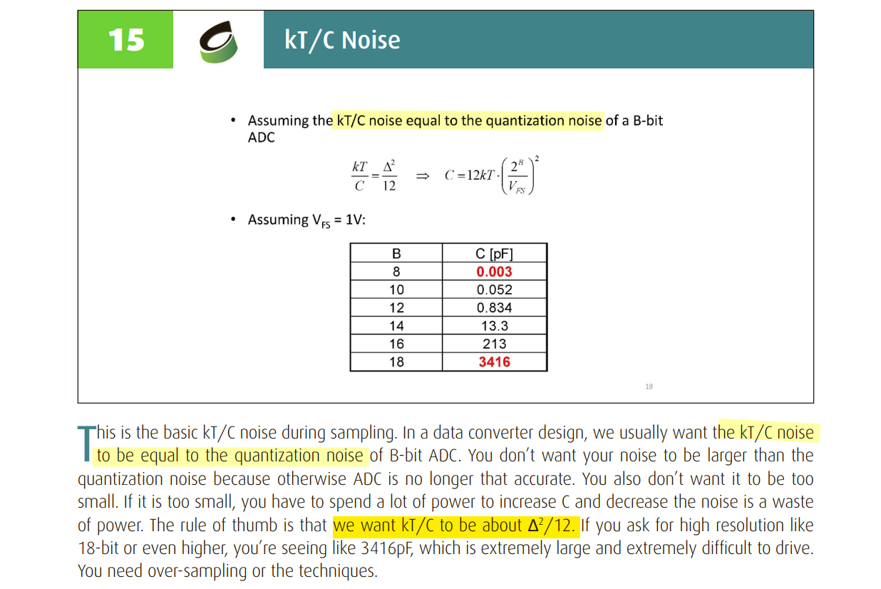
kT/C Noise in sampling
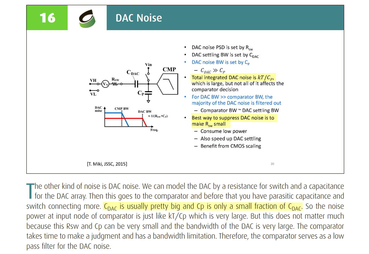
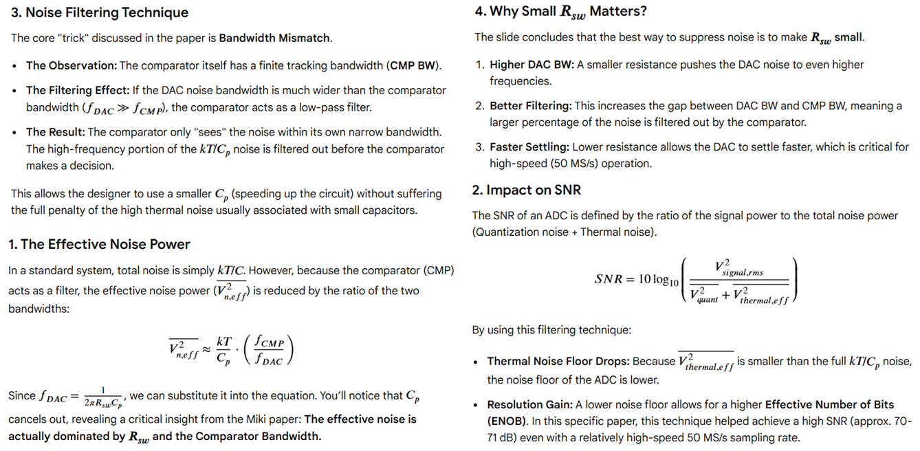
DAC Noise in conversion
T. Miki et al., "A 4.2 mW 50 MS/s 13 bit CMOS SAR ADC With SNR and SFDR Enhancement Techniques," in IEEE Journal of Solid-State Circuits, vol. 50, no. 6, pp. 1372-1381, June 2015 [https://sci-hub.jp/10.1109/JSSC.2015.2417803]
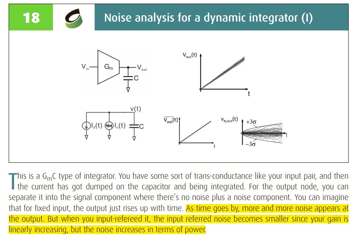
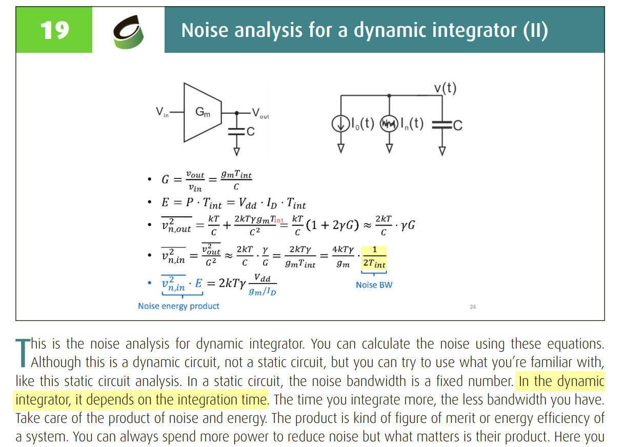
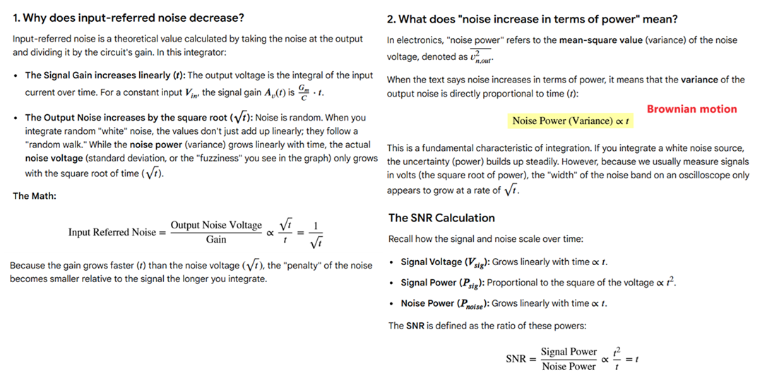
Comparator Noise in conversion
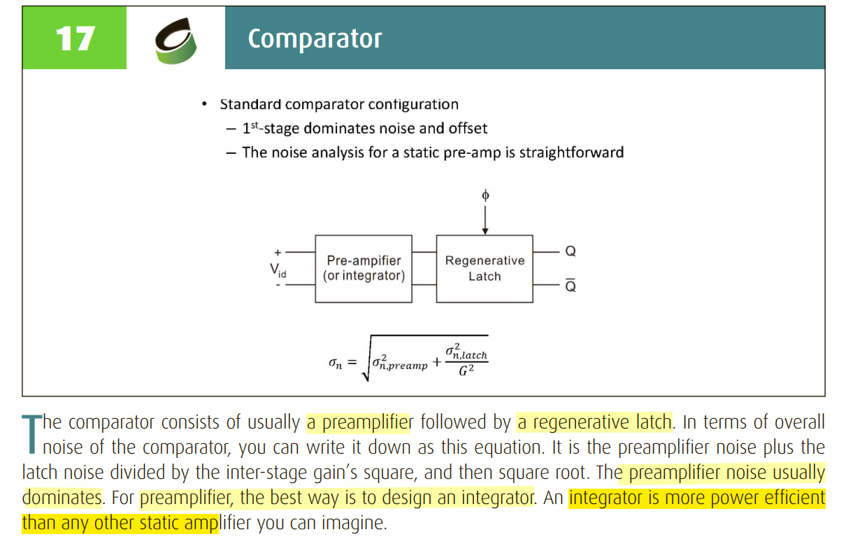
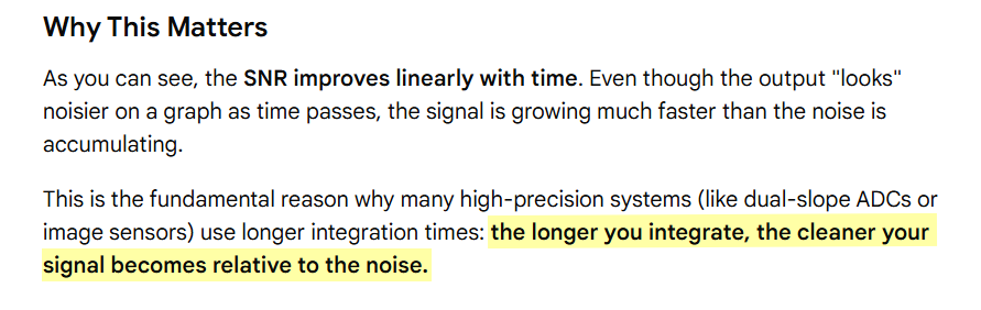
noise analysis for dynamic integrator
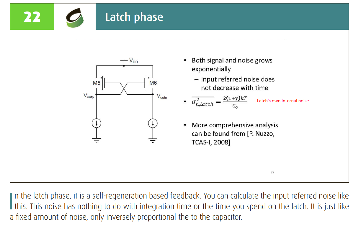
noise analysis for latch phase
P. Nuzzo, F. De Bernardinis, P. Terreni and G. Van der Plas, "Noise Analysis of Regenerative Comparators for Reconfigurable ADC Architectures," in IEEE Transactions on Circuits and Systems I: Regular Papers, vol. 55, no. 6, pp. 1441-1454, July 2008
Comparator
Comparator input cap effect
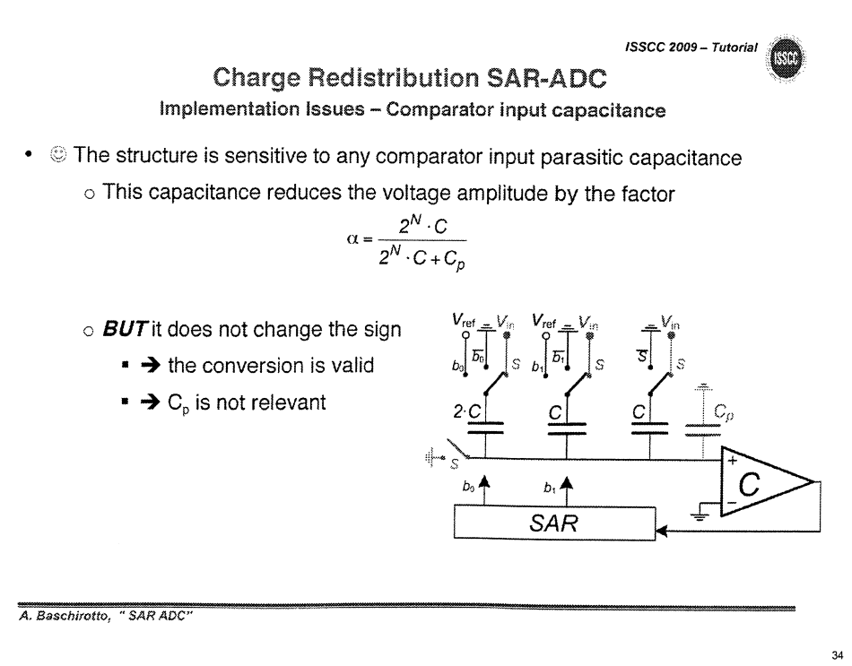 \[
-V_{in}\cdot 2^N C = V_c (2^N C + C_p)
\] Then \(V_c = -\frac{2^N C}{2^N C +
C_p}V_{in}\), i.e. this capacitance reduce the voltage amplitude
by the factor
\[
-V_{in}\cdot 2^N C = V_c (2^N C + C_p)
\] Then \(V_c = -\frac{2^N C}{2^N C +
C_p}V_{in}\), i.e. this capacitance reduce the voltage amplitude
by the factor
During conversion \[\begin{align} V_c &= -\frac{2^N C}{2^N C + C_p}V_{in} +V_{ref}\sum_{n=0}^{N-1} \frac{b_n\cdot2^n C}{2^N C + C_p} \\ &= \frac{2^N C}{2^N C + C_p}\left(-V_{in} + V_{ref}\sum_{n=0}^{N-1}\frac{b_n }{2^{N-n}} \right) \end{align}\]
That is, it does not change the sign
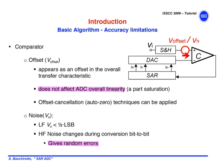
Comparator offset effect
Capacitor DAC (CDAC)
The charge redistribution capacitor network is used to sample the input signal and serves as a digital-to-analog converter (DAC) for creating and subtracting reference voltages
sampling charge \[ Q = V_{in} C_{tot} \] conversion charge \[ Q = -C_{tot}V_c + V_{ref}C_\Delta \] That is \[ V_c = \frac{C_\Delta}{C_{tot}}V_{ref} - V_{in} \]
CDAC is actually working as a capacitive divider during conversion phase, the charge of internal node retain (charge conservation law)
assuming \(\Delta V_i\) is applied to series capacitor \(C_1\) and \(C_2\)
 \[
(\Delta V_i - \Delta V_x) C_1 = \Delta V_x \cdot C_2
\] Then \[
\Delta V_x = \frac{C_1}{C_1+C_2}\Delta V_i
\]
\[
(\Delta V_i - \Delta V_x) C_1 = \Delta V_x \cdot C_2
\] Then \[
\Delta V_x = \frac{C_1}{C_1+C_2}\Delta V_i
\]
\(V_x= V_{x,0} + \Delta V_x\)
CDAC Settling Accuracy
 \[
V_x(s) = \frac{C_1+C_2}{RC_1C_2}\cdot
\frac{1}{s+\frac{C_1+C_2}{RC_1C_2}}\cdot V_i(s) = \frac{1}{\tau}\cdot
\frac{1}{s+\frac{1}{\tau}}\cdot \frac{1}{s}= \frac{1}{\tau}\cdot
\tau(\frac{1}{s} - \frac{1}{s+\frac{1}{\tau}})=\frac{1}{s} -
\frac{1}{s+\frac{1}{\tau}}
\]
\[
V_x(s) = \frac{C_1+C_2}{RC_1C_2}\cdot
\frac{1}{s+\frac{C_1+C_2}{RC_1C_2}}\cdot V_i(s) = \frac{1}{\tau}\cdot
\frac{1}{s+\frac{1}{\tau}}\cdot \frac{1}{s}= \frac{1}{\tau}\cdot
\tau(\frac{1}{s} - \frac{1}{s+\frac{1}{\tau}})=\frac{1}{s} -
\frac{1}{s+\frac{1}{\tau}}
\]
inverse Laplace Transform is \(V_x(t) = 1 - e^{-t/\tau}\)
\[ V_y(s) = V_x\frac{C_1}{C_1+C_2} = \frac{C_1}{C_1+C_2} \left(\frac{1}{s} - \frac{1}{s+\frac{1}{\tau}}\right) \]
inverse Laplace Transform is \(V_y(t) = \frac{C_1}{C_1+C_2}\left(1 - e^{-t/\tau}\right)\)
\(V_x(t)\) and \(V_y(t)\) prove that the settling time is same
\(\tau = R\frac{C_1C_2}{C_1+C_2}\), which means usually worst for MSB capacitor (largest)
both \(\tau\) and \(\Delta V\) are the maximum
A popular way to improve the settling behavior, again, is to employ unit-element DACs that statistically reduce the switching activities, which, unfortunately, exhibits unnecessary complications to the power, area and speed tradeoffs of the design
In a SAR conversion the DAC doesn't move by full scale — the MSB trial is the largest single step, and it is exactly half of full scale. Subsequent trials step by \(V_{FS}/4\), \(V_{FS}/8\), … So the MSB transition (\(\color{red}0 \to V_{FS}/2\)) is the worst case, and if it settles in the allotted per-bit time, every later trial does too.
The accuracy criterion
The settling error must stay below half an LSB, where \(\text{LSB} = V_{FS}/2^{n}\):
\[ \frac{V_{FS}}{2} - V_{DAC}(t_{settle}) \;\le\; \frac{1}{2}\cdot\frac{V_{FS}}{2^{n}} = \frac{V_{FS}}{2^{\,n+1}} \]
Rearranged \[ V_{DAC}(t_{settle}) \ge V_{FS}\left(\frac{1}{2}-\frac{1}{2^{n+1}}\right) \]
Solving for the time \[ \frac{V_{FS}}{2}e^{-t_{settle}/\tau} \le \frac{V_{FS}}{2^{\,n+1}} \;\Longrightarrow\; e^{-t_{settle}/\tau} \le 2^{-n} \]
\[ \boxed{\;t_{settle} \ge n\,\tau\ln 2 \approx 0.693\,n\,\tau\;} \]
| \(n\) | 8 | 10 | 12 | 14 | 16 |
|---|---|---|---|---|---|
| \(t_{settle}/\tau\) | 5.5 | 6.9 | 8.3 | 9.7 | 11.1 |
CDAC Energy calculation
Rabuske, Taimur & Fernandes, Jorge. (2016). "Appendix: Voltage and Energy in CR ADCs", Charge-Sharing SAR ADCs for Low-Voltage Low-Power Applications. 10.1007/978-3-319-39624-8.
\[ E_{Vref} = \int P(t)dt = \int V_{ref} I(t) dt = V_{ref}\int I(t)dt = V_{ref}\cdot \Delta Q \]
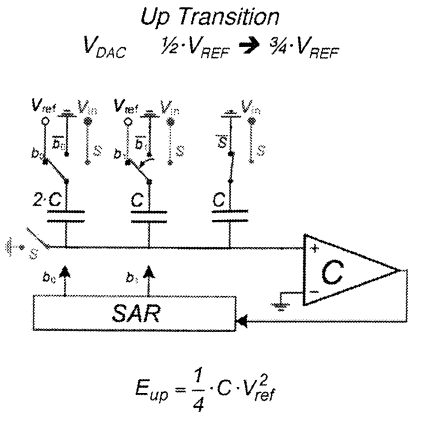
Given \(V_{c,0}=\frac{1}{2}V_{ref}-V_{in}\) and \(V_{c,1}=\frac{3}{4}V_{ref}-V_{in}\) \[\begin{align} Q_{b0,0} &= \left(V_{ref} - V_{c,0} \right)\cdot 2C = \left(\frac{1}{2}V_{ref}+V_{in} \right)\cdot 2C \\ Q_{b1,0} &= (0 - V_{c,0})\cdot C = \left(-\frac{1}{2}V_{ref}+V_{in} \right)\cdot C \\ Q_{b0,1} &= \left(V_{ref} - V_{c,1} \right)\cdot 2C = \left(\frac{1}{4}V_{ref}+V_{in} \right)\cdot 2C \\ Q_{b1,1} &= \left(V_{ref} - V_{c,1} \right)\cdot C = \left(\frac{1}{4}V_{ref}+V_{in} \right)\cdot C \end{align}\]
Therefore \[ E_{Vref} = V_{ref}\cdot (Q_{b0,1}+Q_{b1,1} - Q_{b0,0}-Q_{b1,0}) = \frac{1}{4}C V_{ref}^2 \]
CDAC total energy change \[\begin{align} \Delta E_{tot} &= \frac{1}{2}\cdot 2C \cdot (U_{2c,1}^2 - U_{2c,0}^2) + \frac{1}{2}\cdot C \cdot (U_{c,1}^2 - U_{c,0}^2) + \frac{1}{2}\cdot C \cdot (U_{c1,1}^2 - U_{c1,0}^2) \\ &= \left(-\frac{3}{16}V_{ref}^2 - \frac{1}{2}V_{ref}V_{in} - \frac{3}{32}V_{ref}^2+\frac{3}{4}V_{ref}V_{vin} + \frac{5}{32}V_{ref}^2-\frac{1}{4}V_{ref}V_{in}\right)C \\ &= -\frac{1}{8}CV_{ref}^2 \end{align}\]
alternative method
 \[
\Delta E_{tot} = \frac{1}{2}\cdot\frac{3}{4}C\cdot
V_{ref}^2 - \frac{1}{2}\cdot C\cdot V_{ref}^2 = -\frac{1}{8}CV_{ref}^2
\]
\[
\Delta E_{tot} = \frac{1}{2}\cdot\frac{3}{4}C\cdot
V_{ref}^2 - \frac{1}{2}\cdot C\cdot V_{ref}^2 = -\frac{1}{8}CV_{ref}^2
\]
The total energy decreases by \(-\frac{1}{8}CV_{ref}^2\), though \(V_{ref}\) provides \(\frac{1}{4}C V_{ref}^2\)
The charge redistribution change the CDAC energy

\[ E_{c,0} = \frac{1}{2}CV^2 \] After charge redistribution \[ E_{c,1} = \frac{1}{2}\cdot 2C\cdot \left(\frac{1}{2}V\right)^2 = \frac{1}{4}CV^2 \]
That make sense, charge redistribution consume energy
Binary-Weighted (BW) DAC
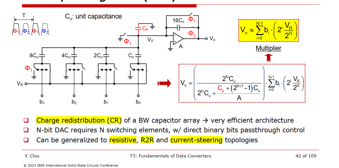
During \(\Phi_1\), all capacitor are shorted, the net charge at \(V_x\) is 0
During \(\Phi_2\), the charge at bottom plate of CDAC \[ Q_{DAC,btm} = \sum_{i=0}^{N-1}(b_i\cdot V_R - V_x)\cdot 2^{i}C_u = C_uV_R\sum_{i=0}^{N-1}b_i2^i - (2^N-1)C_uV_x \] the charge at the internal plate of integrator \[ Q_{intg} = V_x C_p + (V_x - V_o)2^NC_u \] and we know \(-V_x A = V_o\) and \(Q_{DAC,btm} = Q_{intg}\) \[ C_uV_R\sum_{i=0}^{N-1}b_i2^i - (2^N-1)C_uV_x = V_x C_p + (V_x - V_o)2^NC_u \] i.e. \[ C_uV_R\sum_{i=0}^{N-1}b_i2^i = (2^N-1)C_uV_x + V_x C_p + (V_x - V_o)2^NC_u \] therefore \[ -V_o = \frac{2^N C_u}{\frac{(2^{N+1}-1)C_u+C_p}{A}+2^NC_u}\sum_{i=0}^{N-1}b_i\left(2^i\frac{V_R}{2^N}\right)\approx \sum_{i=0}^{N-1}b_i\left(2^i\frac{V_R}{2^N}\right) \]
Midscale (MSB Transition) often is the largest DNL error
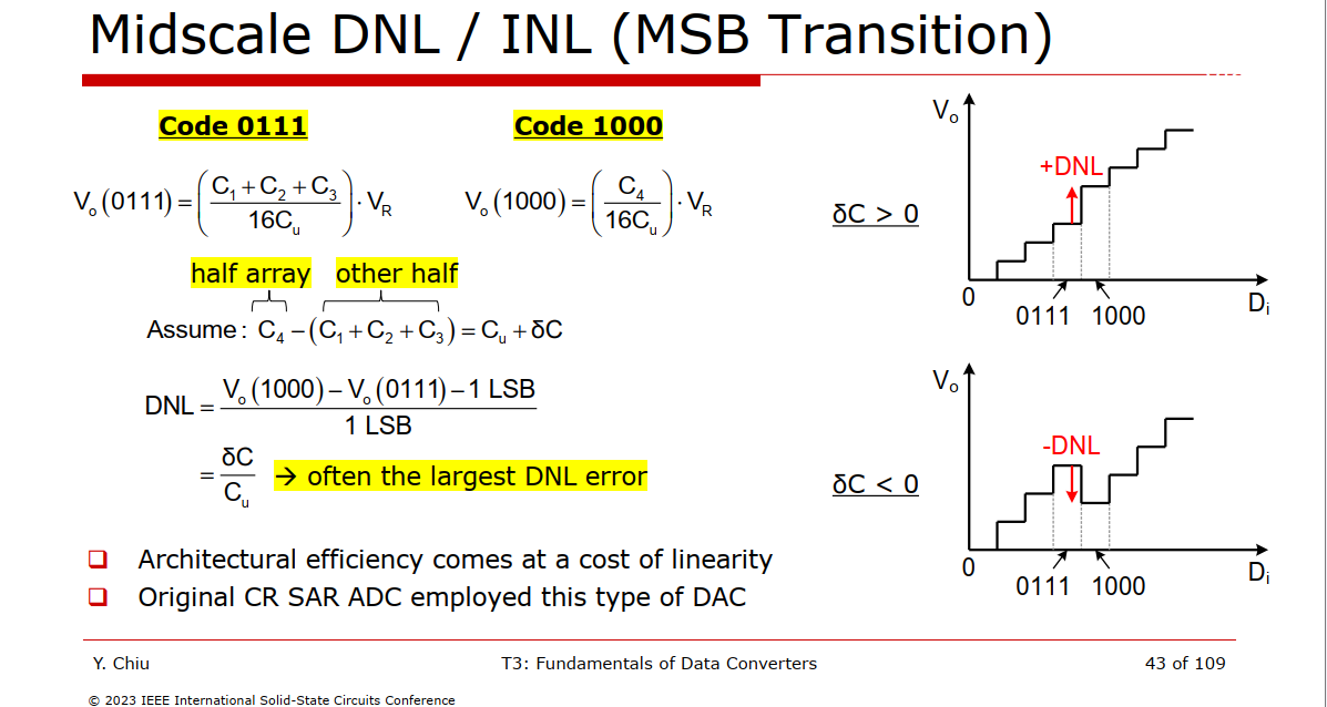
\(C_4\) and \(C_1+C_2+C_3\) are independent (can't cancel out) and their variance is two largest (\(16\sigma_u^2\), \(15\sigma_u^2\), ), the total standard deviation is \(\sqrt{16\sigma_u^2+15\sigma_u^2}=\sqrt{31}\sigma_u\)
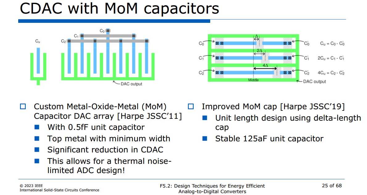
CDAC with Custom MoM
P. J. A. Harpe et al., "A 26 μ W 8 bit 10 MS/s Asynchronous SAR ADC for Low Energy Radios," in IEEE Journal of Solid-State Circuits, vol. 46, no. 7, pp. 1585-1595, July 2011 [https://sci-hub.ru/10.1109/JSSC.2011.2143870]
P. Harpe, "A Compact 10-b SAR ADC With Unit-Length Capacitors and a Passive FIR Filter," in IEEE Journal of Solid-State Circuits, vol. 54, no. 3, pp. 636-645, March 2019 [https://sci-hub.ru/10.1109/JSSC.2018.2878830]
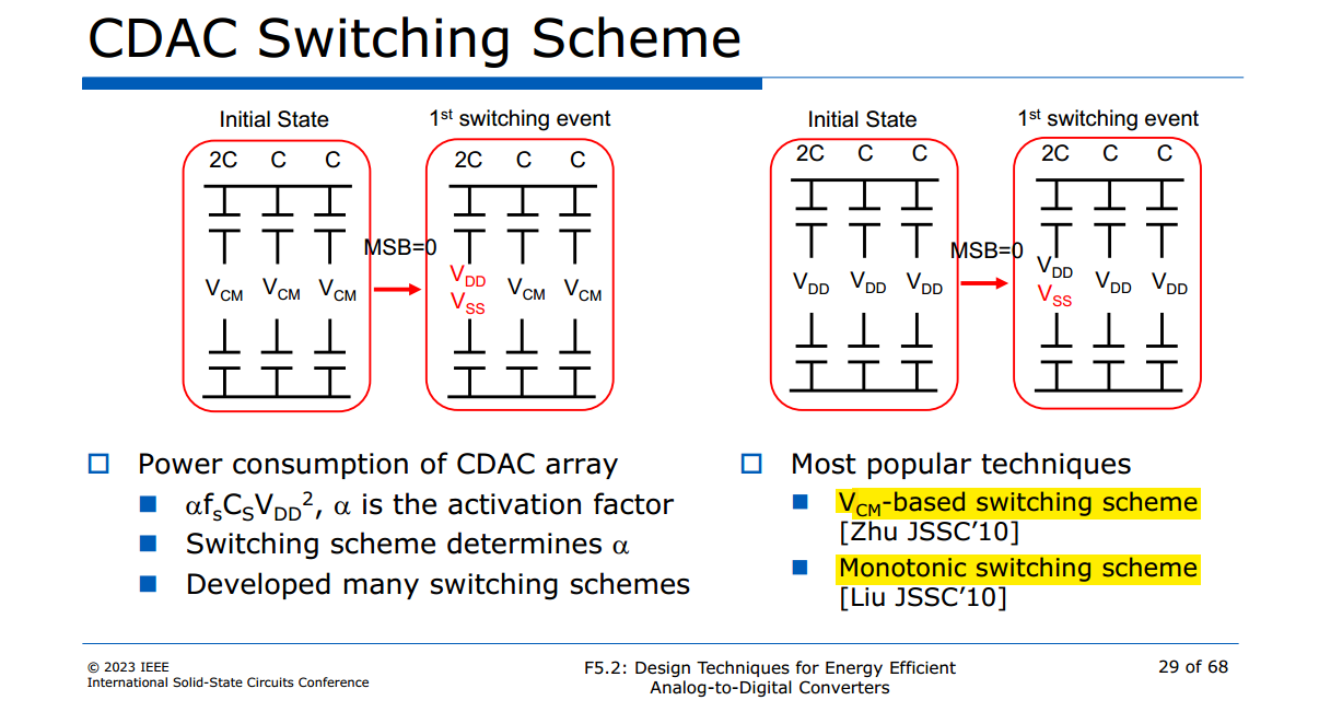
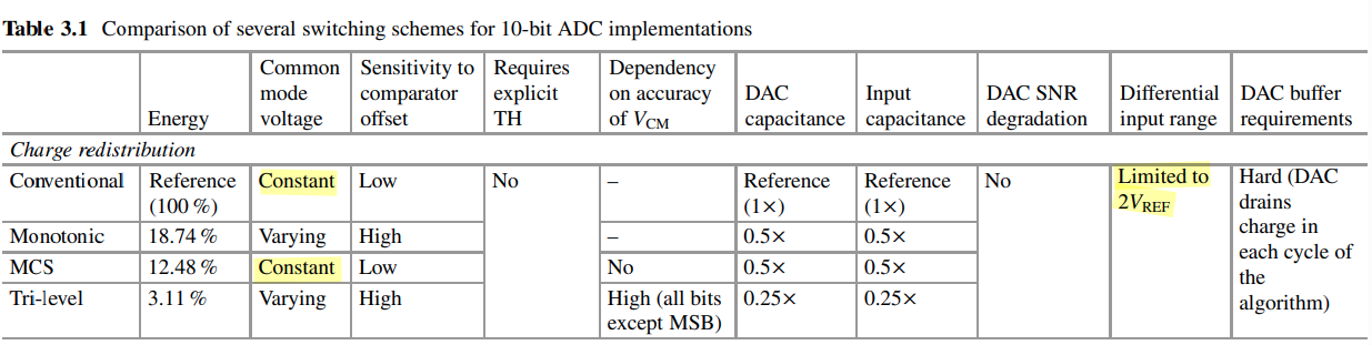
CR Switching Schemes
Hariprasath, V., Jon Guerber, Seunghoon Lee and Un-Ku Moon. “Merged capacitor switching based SAR ADC with highest switching energy-efficiency.” Electronics Letters 46 (2010): 620-621. [https://sci-hub.ru/10.1049/EL.2010.0706]
Y. Zhu et al., "A 10-bit 100-MS/s Reference-Free SAR ADC in 90 nm CMOS," in IEEE Journal of Solid-State Circuits, vol. 45, no. 6, pp. 1111-1121, June 2010 [https://sci-hub.ru/10.1109/JSSC.2010.2048498]
C. -C. Liu, S. -J. Chang, G. -Y. Huang and Y. -Z. Lin, "A 10-bit 50-MS/s SAR ADC With a Monotonic Capacitor Switching Procedure," in IEEE Journal of Solid-State Circuits, vol. 45, no. 4, pp. 731-740, April 2010 [https://sci-hub.ru/10.1109/JSSC.2010.2042254]
Rabuske, Taimur & Fernandes, Jorge. (2017). "Review of SAR ADC Switching Schemes" Charge-Sharing SAR ADCs for Low-Voltage Low-Power Applications. 10.1007/978-3-319-39624-8. [https://sci-hub.ru/10.1007/978-3-319-39624-8_3]
Ramkaj, A.T.; Pelgrom, M.J.M.; Steyaert, M.S.J.; Tavernier, F. Multi-Gigahertz Nyquist Analog-to-Digital Converters: Architecture and Circuit Innovations in Deep-Scaled CMOS and FinFET Technologies; Springer International Publishing: Berlin/Heidelberg, Germany, 2023.
Charge Redistribution (CR) Switching Schemes:
Conventional CR switching scheme: No CM variation
Monotonic switching scheme: Single-ended operation with CM varies 50%VFS
VCM-based switching scheme, a.k.a merged capacitor switching (MCS): No CM variation
Conventional (trial-and-keep) switches the trial capacitor in first, then compares. If the result says the trial overshot, it switches that capacitor back out and inserts the next one. Bits are stored as which capacitors stay connected to \(V_{REF}\)
Monotonic (compare-then-move) compares first, with no trial applied. Then it discharges the next capacitor (from \(V_{REF}\) to ground) on whichever side is higher. That move is never undone; it simply sets up the next comparison
Conventional Switching
bottom-plate sampling
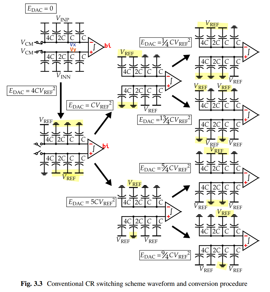
The comparator common mode is \(V_{CM} + V_{REF}/2 − V_{in,cm}\)
Node voltages after the MSB switching
Each array has \(8C\) in total (\(4C + 2C + C + C\), counting the dummy unit cap). During sampling, the top plates sit at \(V_{CM}\) and the bottom plates sit at the input.
For the top (P) array, the charge is \(8C(V_{CM} − V_{INP})\). Then \(4C\) is switched to \(V_{REF}\) and \(4C\) to ground. Charge conservation gives:
\[ 8C\,V_x - 4C\,V_{REF} = 8C\,(V_{CM} - V_{INP}) \;\Rightarrow\; V_x = V_{CM} - V_{INP} + \tfrac{V_{REF}}{2} \]
For the bottom (N) array, the \(4C\) goes to ground and the remaining \(4C (2C + C + C)\) goes to \(V_{REF}\). So you get the same form:
\[ V_y = V_{CM} - V_{INN} + \tfrac{V_{REF}}{2} \]
Common mode \[ \frac{V_x + V_y}{2} = V_{CM} + \frac{V_{REF}}{2} - \frac{V_{INP} + V_{INN}}{2} = V_{CM} + \frac{V_{REF}}{2} - V_{in,cm} \]
You can't drop the input common-mode term. The figure assumes the top-plate sampling voltage equals the input common mode (\(V_{CM} = V_{in,cm} = 0.5\) V). Those two cancel, and the comparator common mode is simply \(V_{REF}/2 = 0.5\) V. That is why both waveforms start at 0.5 V during sampling and converge back to 0.5 V.
Check against the plot
With \(V_{INP} = 0.9\) V, \(V_{INN} = 0.1\) V, \(V_{CM} = 0.5\) V, and \(V_{REF} = 1\) V:
- \(V_x = 0.5 − 0.9 + 0.5 = 0.1\) V (blue trace)
- \(V_y = 0.5 − 0.1 + 0.5 = 0.9\) V (orange trace)
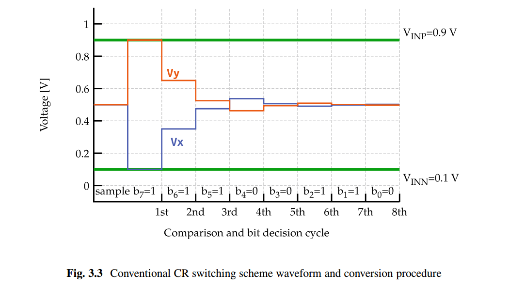
Generalizing equation with trial-and-keep \[\begin{align} V_x^{(k)} &= V_{CM} - V_{INP} + \textcolor{red}{\sum_{i=1}^{k} b_i\,\Delta V_i} \\ V_y^{(k)} &= V_{CM} - V_{INN} + V_{REF} - \textcolor{red}{\sum_{i=1}^{k} b_i\,\Delta V_i} \qquad \qquad \Delta V_i = \frac{V_{REF}}{2^i} \end{align}\]
where \[ b_k = \begin{cases} 1 & \text{if } V_y^{(k)} \ge V_x^{(k)} \color{red}\text{ with trial } b_k = 1 \\ 0 & \text{otherwise (\textcolor{red}{trial reverted})} \end{cases} \]
For simplicity, the final term \(\color{blue}(b[0]-1)\cdot 1\text{LSB}\) of the general equation \(D_{out} = s(M) + \sum_{i=1}^{M-1}(2\cdot b[i] - 1)\times s(i) + (b[0] -1)\cdot \text{1LSB}\) is approximated as \(\color{red}(2b[0] -1)\cdot\frac{\text{1LSB}}{2}\)
During bit cycling, \(V_y - V_x \to 0\), i.e. \[ 2 \textcolor{red}{\sum b_i \Delta V_i } - \textcolor{blue}{V_{REF}}\qquad \Longrightarrow \qquad V_{INP} - V_{INN} \] After N = 8 bits: \[ V_{INP} - V_{INN} = V_{REF}\left(2\sum_{i=1}^{8} b_i\,2^{-i} - 1\right) + \varepsilon, \qquad 0 \le \varepsilon < \frac{2V_{REF}}{2^8} = \mathrm{1 LSB} \] For the complete 8-bit conversion shown in Fig. 3.3 \[ 2\times \left(\frac{1}{2}\times1+\frac{1}{4}\times1+\frac{1}{8}\times1+\frac{1}{16}\times0+\frac{1}{32}\times0+\frac{1}{64}\times1+\frac{1}{128}\times1+\frac{1}{256}\times0\right)-1 = \frac{204}{256} \] i.e. \[ \left|\frac{204}{256} - 0.8\right| \qquad \lt \qquad \mathrm{1LSB} \]
Monotonic Switching
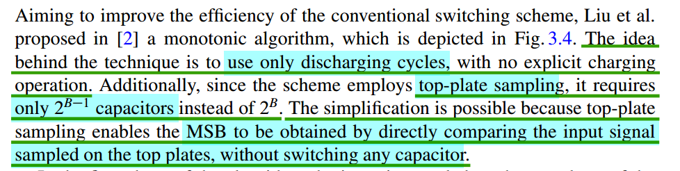
top-plate sampling; use only discharging cycles
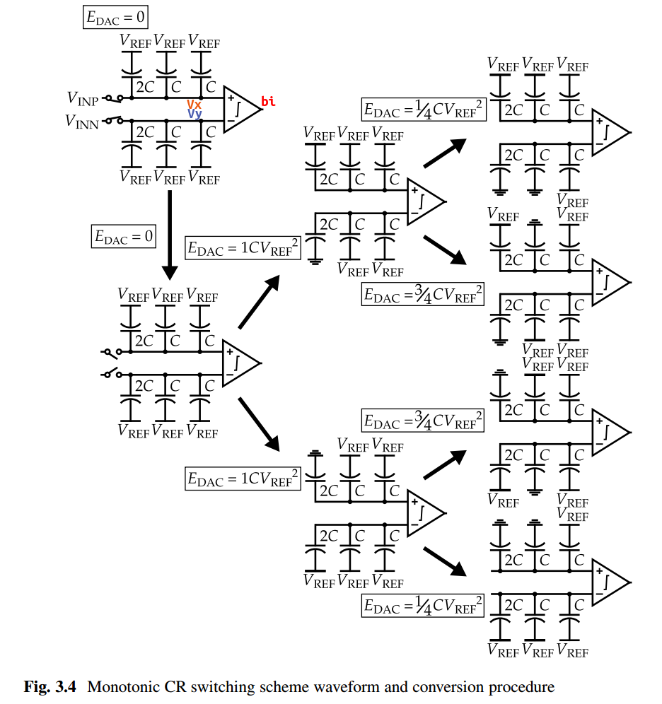
\[\begin{align} V_x^{(k)} &= V_{INP} - \textcolor{red}{\sum_{i=1}^{k} b_i\,\Delta V_i} \\ V_y^{(k)} &= V_{INN} - \textcolor{red}{\sum_{i=1}^{k} (1-b_i)\,\Delta V_i} \qquad \qquad \Delta V_i = \frac{V_{REF}}{2^i} \end{align}\]
where \[ b_k = \begin{cases} 1 & \text{if } V_x^{(k-1)} \ge V_y^{(k-1)} \\ 0 & \text{otherwise } \end{cases} \] During bit cycling, \(V_y - V_x \to 0\), i.e. \[ \textcolor{red}{\sum (2b_i-1) \Delta V_i } \qquad \Longrightarrow \qquad V_{INP} - V_{INN} \] For the monotonic result
\[ V_{REF}\sum (2b_k - 1)\,2^{-k} = 2V_{REF}\sum b_k 2^{-k}-V_{REF} + \color{red}\tfrac{V_{REF}}{2^N} \]
so the relationship between Conventional and monotonic result \[ V_\text{monotonic} = V_\text{Conventional} + \color{red}\frac{\mathrm{1 LSB}}{2} \] For the complete 8-bit conversion of monotonic scheme shown in Fig. 3.4 \[ \frac{1}{2}+\frac{1}{4}+\frac{1}{8}-\frac{1}{16}-\frac{1}{32}+\frac{1}{64}+\frac{1}{128}-\frac{1}{256} = \frac{204}{256} + \color{red}\frac{1}{256} \]
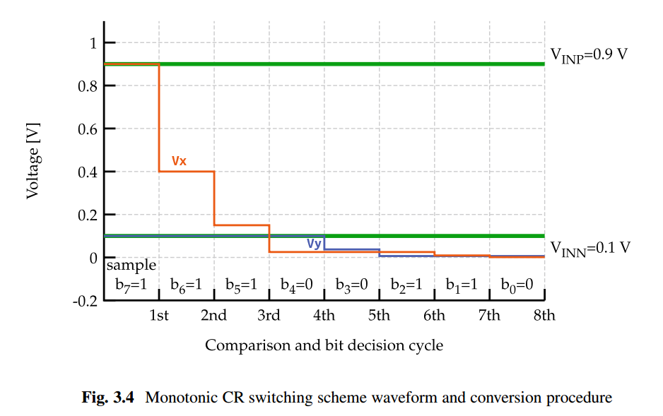
3-bit conversion of monotonic switching scheme as Fig.3.4 drawn

VCM-Based Capacitor Switching
top-plate sampling; No CM variation
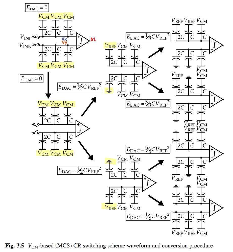
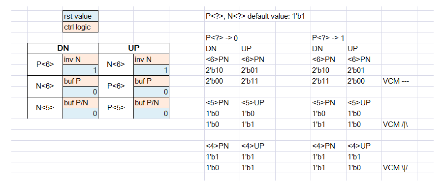
\(V_{CM} \to V_{REF} \text{ or } 0\)
\[\begin{align} V_x^{(k)} &= V_{INP} - \textcolor{red}{\sum_{i=1}^{k} b_i\,\Delta V_{\downarrow,i}} + \textcolor{red}{\sum_{i=1}^{k} (1-b_i)\,\Delta V_{\uparrow,i}} \\ V_y^{(k)} &= V_{INN} - \textcolor{red}{\sum_{i=1}^{k} (1-b_i)\,\Delta V_{\downarrow,i}}+\textcolor{red}{\sum_{i=1}^{k} b_i\,\Delta V_{\uparrow,i}} \qquad \qquad \Delta V_{\downarrow,i} = \frac{V_{CM}}{2^i}\quad \Delta V_{\uparrow,i} = \frac{V_{REF}-V_{CM}}{2^i} \end{align}\]
where \[ b_k = \begin{cases} 1 & \text{if } V_x^{(k-1)} \ge V_y^{(k-1)} \\ 0 & \text{otherwise } \end{cases} \] During bit cycling, \(V_y - V_x \to 0\), i.e. \[ \textcolor{red}{\sum (2b_i-1) \Delta V_{\downarrow,i} + \sum (2b_i-1) \Delta V_{\uparrow,i}} \qquad \Longrightarrow \qquad V_{INP} - V_{INN} \] When \(V_{CM}\) is precisely half of \(V_{REF}\) \[ \Delta V_{\downarrow,i} = \Delta V_{\uparrow,i} = \frac{V_{REF}}{2^{i+1}} \] then \[ V_{INP} - V_{INN} \approx \sum (2b_i-1) \frac{V_{REF}}{2^{i}} \]
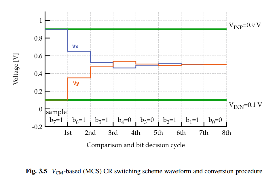
CDAC with constant common-mode voltage

Synchronous SAR ADC
It also divides a full conversion into several comparison stages in a way similar to the pipeline ADC, except the algorithm is executed sequentially rather than in parallel as in the pipeline case.
However, the sequential operation of the SA algorithm has traditionally been a limitation in achieving high-speed operation
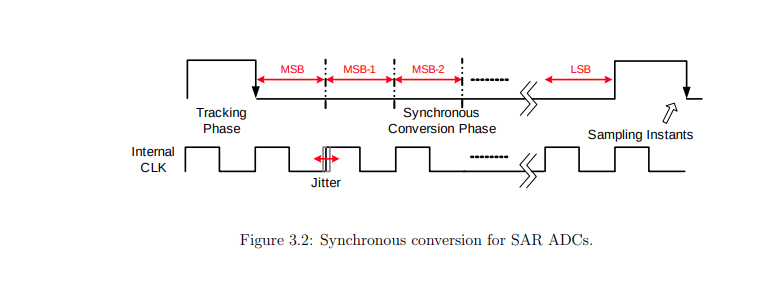
- a clock running at least \((N + 1) \cdot F_s\) is required for an \(N\)-bit converter with conversion rate of \(F_s\)
- every clock cycle has to tolerate the worst case comparison time
- every clock cycle requires margin for the clock jitter
The power and speed limitations of a synchronous SA design comes largely from the high-speed internal clock
Split Arrary CDAC
Split capacitor, double-array cap
attenuation capacitance \(C_a\)
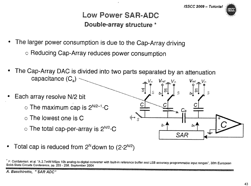
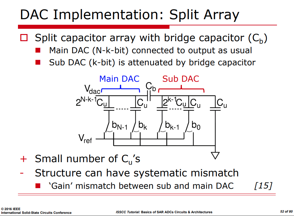

\[ \Delta V_{dac} = \frac{1}{2}b_3+\frac{1}{4}b_2+\frac{1}{4}\left(\frac{1}{2}b_1+\frac{1}{4}b_0 \right) = \frac{1}{2}b_3+\frac{1}{4}b_2 + \frac{1}{8}b_1+\frac{1}{16}b_0 \]
Asynchronous SAR ADC
Mike Shuo-Wei Chen and R. W. Brodersen, "A 6-bit 600-MS/s 5.3-mW Asynchronous ADC in 0.13-μm CMOS," in IEEE Journal of Solid-State Circuits, vol. 41, no. 12, pp. 2669-2680, Dec. 2006 [pdf, slides]
—. "Power Efficient System and A/D Converter Design for Ultra-Wideband Radio" [http://www2.eecs.berkeley.edu/Pubs/TechRpts/2006/EECS-2006-71.pdf]
—. "Asynchronous SAR ADC: Past, Present and Beyond"
H. Karrari, P. Andreani and S. Tan, "Asynchronous vs Synchronous SAR ADCs – Performance Beyond Nominal Speed," 2024 19th Conference on Ph.D Research in Microelectronics and Electronics (PRIME), Larnaca, Cyprus, 2024, pp. 1-4, doi: 10.1109/PRIME61930.2024.10559690.
The comparator itself trigger the next bit-conversion cycle as soon as the present bit decision has been taken
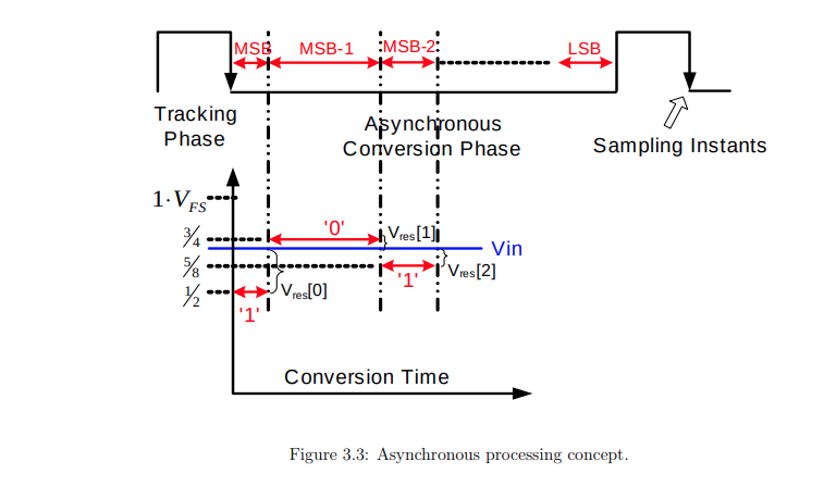
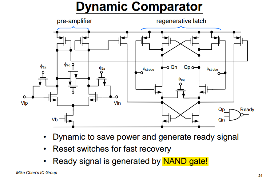
The maximum resolving time reduction between synchronous and asynchronous case is two fold
comparator metastable state
when the input is sufficiently small. The time needed for the comparator outputs to fully resolve may take arbitrarily long
In this case, the ready signal generator should still set the flag and the decision result is simply taken from the previous value stored in the SR latch
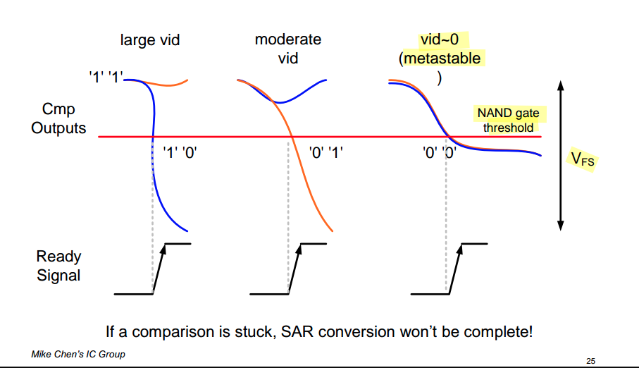
both outputs (\(Q_p\) and \(Q_n\)) will drop together, NAND is inverter actually
The transition point of this NAND gate is skewed to eliminate metastability issues arising when the input differential voltage level is small (comparator)
Redundancy with Radix
Kuttner, Franz. "A 1.2V 10b 20MSample/s non-binary successive approximation ADC in 0.13/spl mu/m CMOS." 2002 IEEE International Solid-State Circuits Conference. Digest of Technical Papers (Cat. No.02CH37315) 1 (2002): 176-177 vol.1. [https://sci-hub.jp/10.1109/ISSCC.2002.992993]
M. Hesener, T. Eicher, A. Hanneberg, D. Herbison, F. Kuttner and H. Wenske, "A 14b 40MS/s Redundant SAR ADC with 480MHz Clock in 0.13pm CMOS," 2007 IEEE International Solid-State Circuits Conference. Digest of Technical Papers, San Francisco, CA, USA, 2007, pp. 248-600 [https://sci-hub.ru/10.1109/ISSCC.2007.373387]
Tomohiko OGAWA et al., SAR ADC Algorithm with Redundancy and Digital Error Correction, IEICE Transactions on Fundamentals of Electronics, Communications and Computer Sciences, 2010, Volume E93.A, Issue 2, Pages 415-423 [https://sci-hub.ru/10.1587/TRANSFUN.E93.A.415]
C. -C. Liu et al., "A 10b 100MS/s 1.13mW SAR ADC with binary-scaled error compensation," 2010 IEEE International Solid-State Circuits Conference - (ISSCC), San Francisco, CA, USA, 2010, pp. 386-387 [https://sci-hub.ru/10.1109/ISSCC.2010.5433970]
—, “Design of High-Speed Energy-Efficient Successive-Approximation Analog-to-Digital Converters,” Ph.D. dissertation, Dept. Elect. Eng., National Cheng Kung University, Tainan, Taiwan, R.O.C., 2010.
—, "A 10 bit 320 MS/s Low-Cost SAR ADC for IEEE 802.11ac Applications in 20 nm CMOS," in IEEE Journal of Solid-State Circuits, vol. 50, no. 11, pp. 2645-2654, Nov. 2015 [https://sci-hub.ru/10.1109/JSSC.2015.2466475]
W. Liu, P. Huang and Y. Chiu, "A 12-bit, 45-MS/s, 3-mW Redundant Successive-Approximation-Register Analog-to-Digital Converter With Digital Calibration," in IEEE Journal of Solid-State Circuits, vol. 46, no. 11, pp. 2661-2672, Nov. 2011 [https://sci-hub.ru/10.1109/JSSC.2011.2163556]
Albert H. Chang, Hae-Seung Lee, and Duane S. Boning. 2011. Redundancy in SAR ADCs. In Proceedings of the 21st edition of the great lakes symposium on Great lakes symposium on VLSI (GLSVLSI '11). Association for Computing Machinery, New York, NY, USA, 283–288. [https://dl.acm.org/doi/10.1145/1973009.1973066]
—, “Low-power high-performance SAR ADC with redundancy and digital background calibration,” Ph.D. dissertation, Dept. Elect. Eng. Comput. Sci., Massachusetts Institute of Technology, Cambridge, MA, USA, 2013. [Online]. [https://dspace.mit.edu/bitstream/handle/1721.1/82177/861702792-MIT.pdf]
B. Murmann, “On the use of redundancy in successive approximation A/D converters,” International Conference on Sampling Theory and Applications (SampTA), Bremen, Germany, July 2013. [https://www.eurasip.org/Proceedings/Ext/SampTA2013/papers/p556-murmann.pdf]
Krämer, M. et al. (2015) High-resolution SAR A/D converters with loop-embedded input buffer. dissertation. Available at: [http://purl.stanford.edu/fc450zc8031].
sarthak, "Visualising redundancy in a 1.5 bit pipeline ADC“ [https://electronics.stackexchange.com/a/523489/233816]
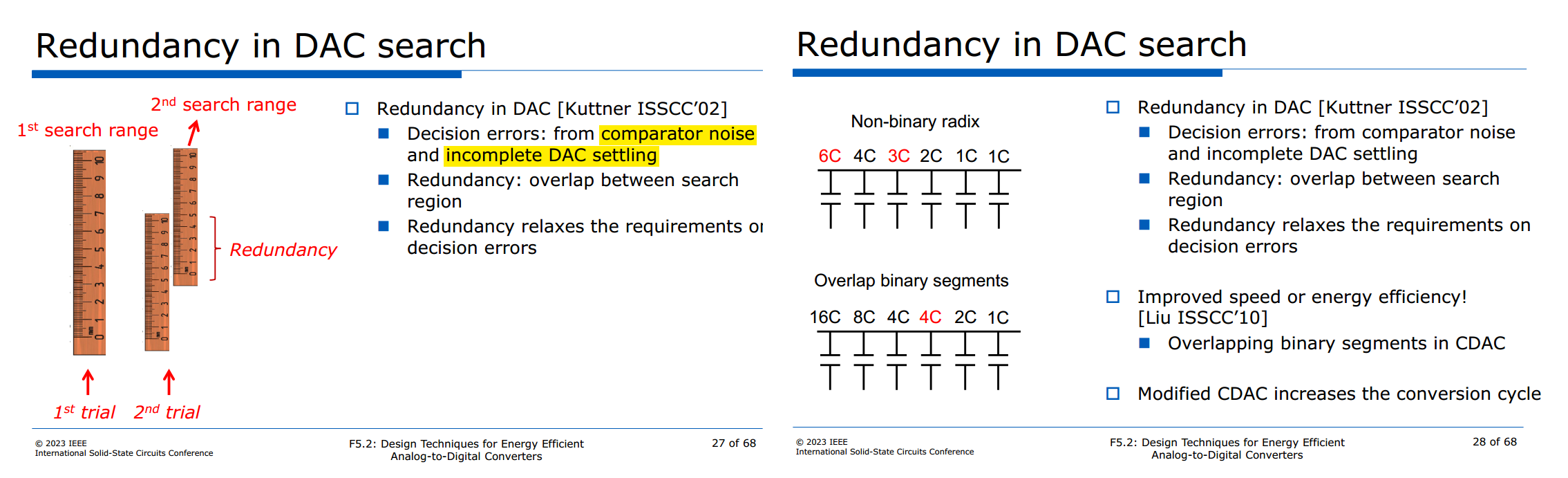
conventional binary SAR ADC
- After each DAC switching, the effective input range is reduced by a factor of 2
Kuttner ISSCC'02: non-binary SAR ADC
- the input range is reduced by a factor smaller than 2 per each bit cycle
Liu ISSCC'10: binary-scaled CDAC
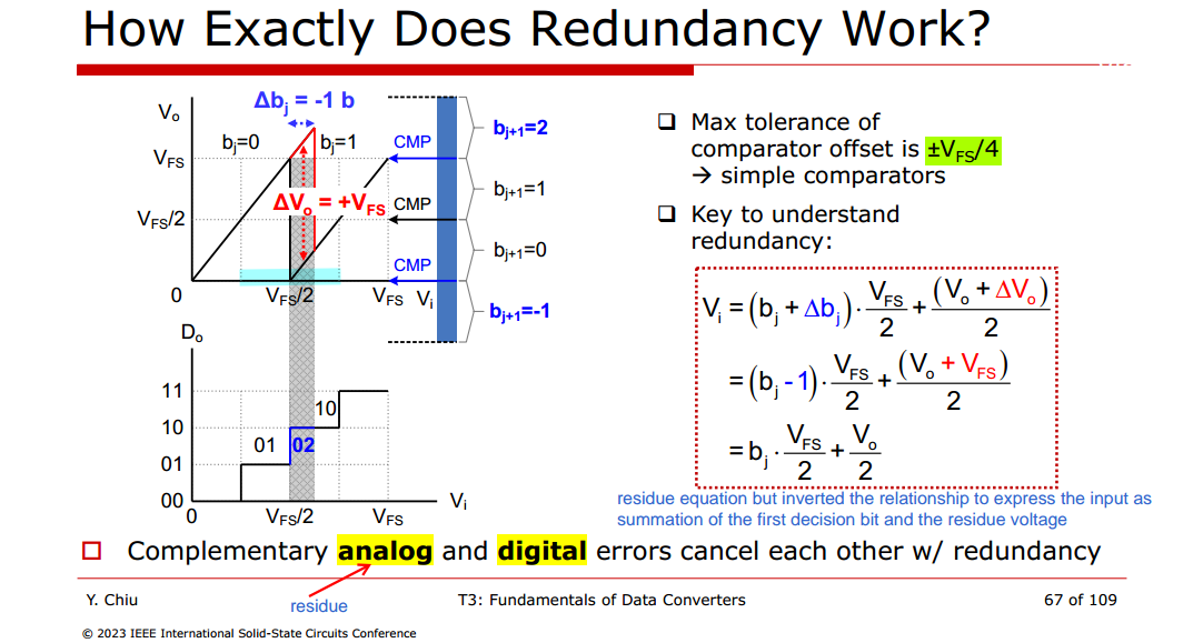
Max tolerance of comparator offset is \(\pm V_{FS}/4\)
- \(b_j\) error is \(\pm 1\)
- \(b_{j+1}\) error is \(\pm 2\) , wherein \(b_{j+1}\): \(0\to 2\) or \(1\to -1\)
i.e. complementary analog and digital errors cancel each other, \(V_o +\Delta V_{o}\) should be in over-/under-range comparators (\(-V_{FS}/2 \sim 3V_{FS}/2\))
\[\begin{align} V_{in,j} &= (b_j + \Delta b_j)\cdot \frac{V_{FS}}{2} + \frac{V_{out,j}+\Delta V_{out,j}}{2} \\ V_{in,{j+1}} &= (b_{j+1} + \Delta b_{j+1})\cdot \frac{V_{FS}}{2} + \frac{V_{out,j+1}+\Delta V_{out,j+1}}{2} \end{align}\]
with \(V_{in,j+1} = V_{out,j}+\Delta V_{out,j}\)
\[\begin{align} V_{in,j} &= (b_j + \Delta b_j)\cdot \frac{V_{FS}}{2} + \frac{1}{2} \left\{ (b_{j+1} + \Delta b_{j+1})\cdot \frac{V_{FS}}{2} + \frac{V_{out,j+1}+\Delta V_{out,j+1}}{2} \right\} \\ &= (b_j + \Delta b_j)\cdot \frac{V_{FS}}{2} + \frac{1}{2}(b_{j+1} + \Delta b_{j+1})\cdot \frac{V_{FS}}{2}+ \frac{1}{2}\frac{V_{in,j+2}}{2} \\ &=\tilde{b_j} \cdot \frac{V_{FS}}{2}+ \tilde{b_{j+1}}\cdot \frac{V_{FS}}{4}+ \frac{1}{4}V_{in,j+2} \end{align}\]
where \(b_j\) is 1-bit residue without redundancy and \(\tilde{b_j}\) is redundant bits
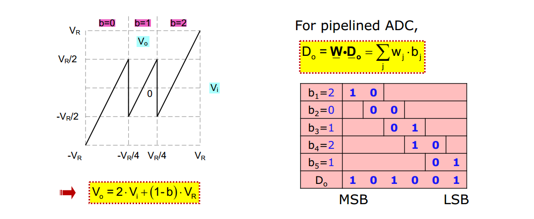
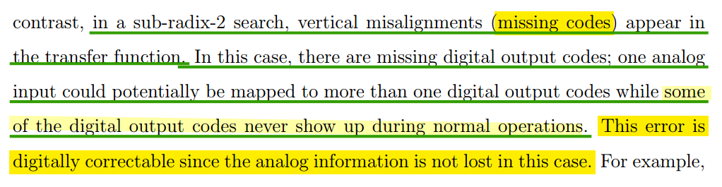
Uniform Sub-Radix-2 SAR ADC
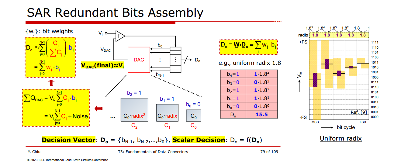
Minimal analog complexity, no additional decoding effort
Search Algorithm
final digital output of \(N\)-bit \(M\)-step ADC \[ \boxed{\color{blue}D_{out} = s(M) + \sum_{i=1}^{M-1}(2\cdot b[i] - 1)\times s(i) + (b[0] -1)\cdot \text{1LSB}} \]
where \(b[M-1]\dots b[0]\) and \(s(M)\dots s(1)\)
| i | M | M-1 | M-2 | ... | 2 | 1 | 0 |
|---|---|---|---|---|---|---|---|
| b[i] | b[M-1] | b[M-2] | ... | b[2] | b[1] | b[0] | |
| s[i] | s(M) | s(M-1) | s(M-2) | ... | s(2) | s(1) |
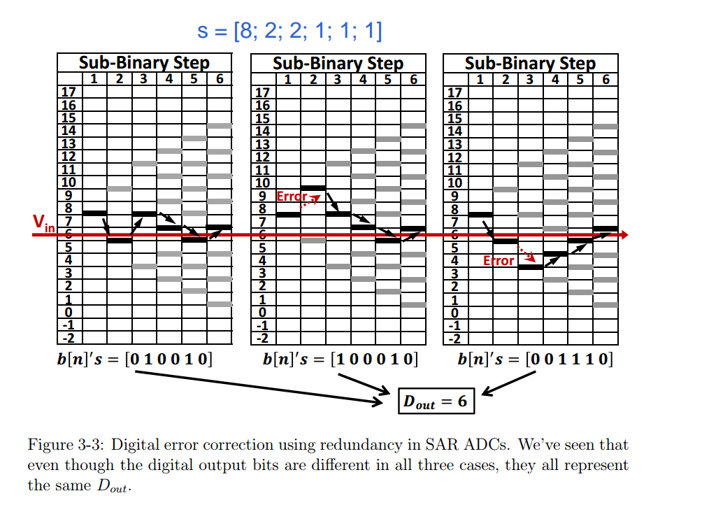
\(N\)-bit binary weighted algorithm
with \(N=M\) and \(s(i)=2^{i-1}\), where \(i\in \{N, N-1,...,2,1 \}\)
\[\begin{align} D_{out} &= s(M) + \sum_{i=1}^{M-1}(2\cdot b[i] - 1)\times s(i) + (b[0] -1) \\ &= 2^{N-1} + \sum_{i=1}^{N-1}2^i\cdot b[i] - \sum_{i=0}^{N-2}2^{i} + (b[0] -1) \\ &= \boxed{\color{blue}\sum_{i=0}^{N-1} b[i] \cdot 2^i} \end{align}\]
Differential ADC: \(s(M) = 0\), i.e. \(w_{M-1} = 0\) (using \(w_i = s(i+1)\))
| \(i\) | \(M-1\) | \(M-2\) | \(\cdots\) | \(2\) | \(1\) | \(0\) |
|---|---|---|---|---|---|---|
| \(b_i\) | \(b_{M-1}\) | \(b_{M-2}\) | \(\cdots\) | \(b_2\) | \(b_1\) | \(b_0\) |
| \(w_i\) | 0 | \(w_{M-2}\) | \(\cdots\) | \(w_2\) | \(w_1\) | \(w_0\) |
| \(W_i\) | \(2w_{M-2}\) | \(2w_{M-3}\) | \(\cdots\) | \(2w_1\) | \(2w_0\) | 1 LSB |
\[\begin{align} D_{out} &= \sum_{i=1}^{M-1}\left(2b_i-1\right)w_{i-1} + \left(b_0-1\right)\cdot 1\,\text{LSB} \\ &= \sum_{i=1}^{M-1}b_i\cdot 2w_{i-1} + b_0\cdot 1\,\text{LSB} - \sum_{i=1}^{M-1}w_{i-1} - 1\,\text{LSB} \\ &= \left[\sum_{i=1}^{M-1}b_i\cdot 2w_{i-1} + b_0\cdot 1\,\text{LSB}\right] - \frac{1}{2}\left[\sum_{i=1}^{M-1}2w_{i-1} + 1\,\text{LSB} + 1\,\text{LSB}\right] \\ &= \boxed{\color{blue}\sum_{i=0}^{M-1}b_i\cdot W_i - \frac{1}{2}\left[\sum_{i=0}^{M-1}W_i + W_0\right]} \end{align}\]
The ADC equivalent weight \(W_i\)
\[ \begin{cases} W_0 = 1\,\text{LSB} \\ W_i = 2w_{i-1}, & \text{for } i \in [1, M-1] \end{cases} \]
Note: when \(\sum_{i=0}^{M-1} W_i = (2^N - 1)\) LSB, the constant term simplifies to \(\frac{1}{2}\left[\sum_{i=0}^{M-1} W_i + W_0\right] = 2^{N-1}\) LSB, so
\[ D_{out} = \sum_{i=0}^{M-1} b_i\cdot W_i - 2^{N-1} \]
which is a signed output in \(\left[-2^{N-1},\ 2^{N-1}-1\right]\) LSB.
Non-Binary Search
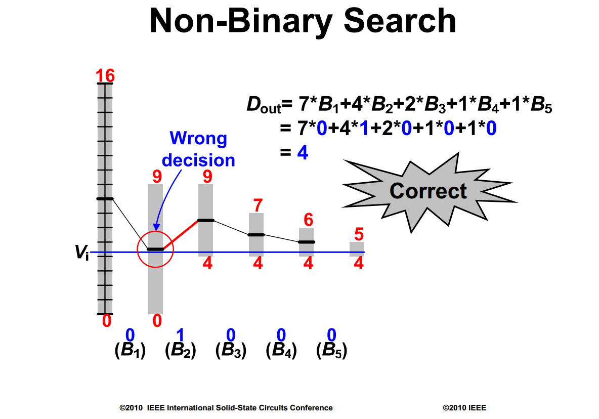
\[\begin{align} D_\text{out} &= 8 + (2B_1-1)\times3.5+ (2B_2-1)\times2+ (2B_3-1)\times1+ (2B_4-1)\times0.5+ (B_5-1)\times1 \\ &= 7B_1+4B_2+2B_3+1B_4+1B_5 \end{align}\]

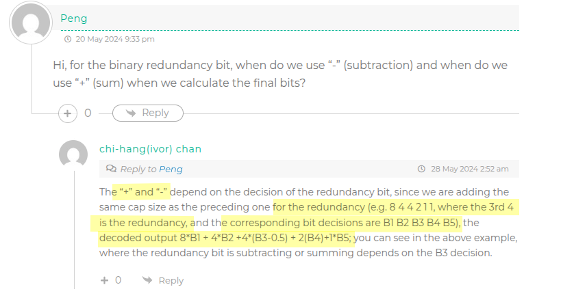
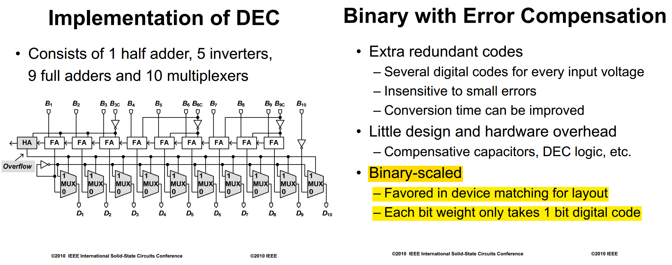
Binary with Error Compensation a.k.a Binary-Scaled Error Compensation
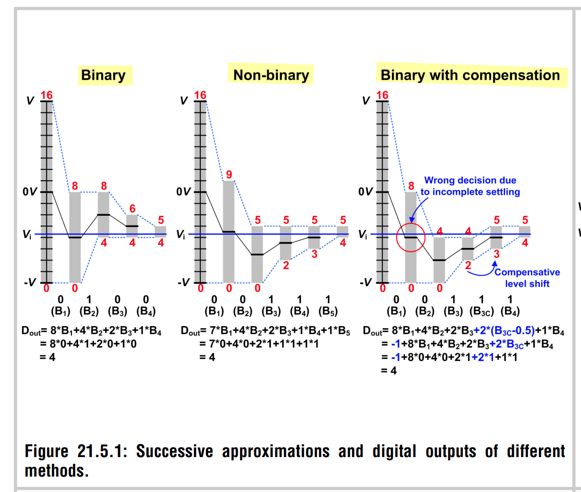
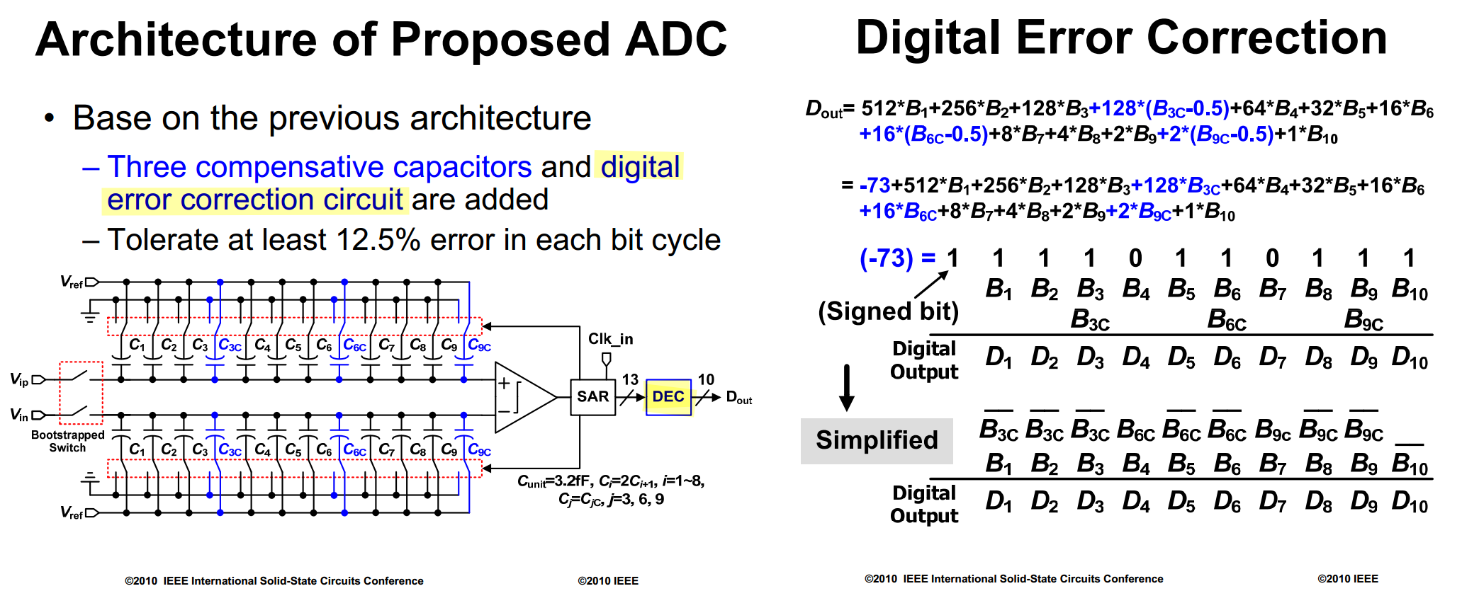
this is the monotonic scheme
Each comparison is followed by switching one capacitor (\(V_{REF} \to \text{ground}\)) on whichever side is higher. That moves the differential DAC voltage by \(\pm w\,u\), where \(w\) is that capacitor's size in unit caps (\(u\) below). The order is:
- B1 → C1 (256), B2 → C2 (128), B3 → C3 (64)
- B3C → C3C (64)
- B4 → C4 (32), B5 → C5 (16), B6 → C6 (8)
- B6C → C6C (8)
- B7 → C7 (4), B8 → C8 (2), B9 → C9 (1)
- B9C → C9C (1)
- B10 → nothing (last decision)
That is 13 decisions, giving the "13b redundant code."
Let one unit cap move the differential by \(u = V_{REF}\cdot C_u/C_{total}\), and let \(w_k = 2^{9-k}\) be the size of \(C_k\). After the last move (C9C) the residue is within \(\pm u\); B10 resolves its sign, so the reconstruction error is within \(\pm u/2\): \[ \frac{V_{in}}{u} \approx \underbrace{\sum_{k=1}^{9} (2B_k-1)\,w_k}_{\text{main caps}} \;+\; \underbrace{(2B_{3C}-1)\,64 + (2B_{6C}-1)\,8 + (2B_{9C}-1)\,1}_{\text{compensation caps}} \;+\; (2B_{10}-1)\tfrac12 \]
The 10-bit input range is \(\color{blue}\pm512u\): \(C_1\sim C_9\) span \(\pm511u\) and B10 resolves the last \(\pm u\). The compensation caps add \(\pm73u\) of over-range (raw code \(-73\dots1096\)), which the DEC clips. Since \(C_{total}\approx584\,C_u\), the full scale is \(\pm\tfrac{512}{584}V_{REF}\approx\pm0.88\,V_{REF}\) (ignoring parasitics)
So the output code, with intentional offset \(511.5\) \[ D_{out} \approx \frac{V_{in}}{u} + \color{red}\left(511+\tfrac12\right) \] which maps the input onto \(0 \dots 1023\)
after cancelling and rearranging
\[\begin{align} D_{out} &= \underbrace{\sum_{k=1}^{9} B_k\cdot2w_k}_{\text{main caps}} \;+\; \underbrace{(2B_{3C}-1)\,64 + (2B_{6C}-1)\,8 + (2B_{9C}-1)\,1}_{\text{compensation caps}} \;+\; B_{10} \\ &= \underbrace{\sum_{k=1}^{9} B_k\cdot2w_k}_{\text{main caps}} \;+\; \textcolor{red}{\underbrace{(B_{3C}-0.5)\,128 + (B_{6C}-0.5)\,16 + (B_{9C}-0.5)\,2}_{\text{compensation caps}}} \;+\; B_{10} \end{align}\]
The relationship between \(D_{out}\) and \(V_{in}\)
\[ \boxed{V_{in} \approx (D_{out} - 511.5)\,u, \qquad u = 1\text{ LSB} = V_{REF}\,\frac{C_u}{C_{total}}} \]
Exactly, with ideal thresholds at integer multiples of u:
\[ \boxed{D_{out} - 512 \;\le\; \frac{V_{in}}{u} \;<\; D_{out} - 511 \quad\Longleftrightarrow\quad D_{out} = \left\lfloor \frac{V_{in}}{u} \right\rfloor + 512} \]
Error Tolerance Window
\[ \varepsilon_t(n) = \sum_{i=1}^{n-2} s(i) - s(n-1) \]
where \(n\in [1, N]\), and \(N\)-bit SAR

For the \(n\)th output bit, once a decision is made, the next decision level will either move up or down by the step size of \(s(n − 1)\)
If this decision is erroneous, then the sum of the follow-on step sizes, \(s(n − 2)\), \(s(n − 3)\), ..., \(s(1)\), must be large enough and exceed the value of the current step size to counteract this mistake
The exceeded amount is the tolerance window for that decision level
sub-binary search
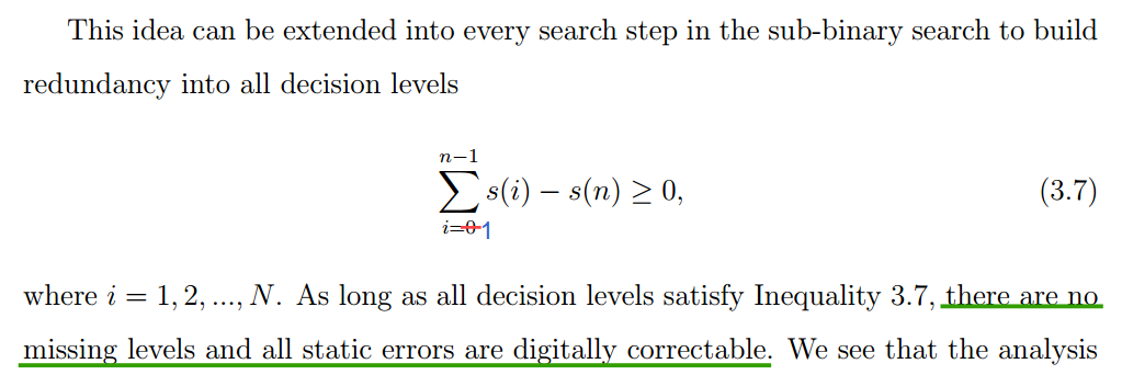
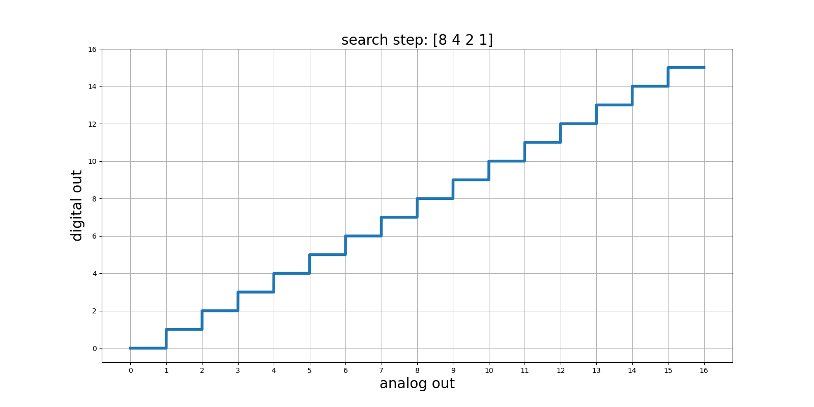
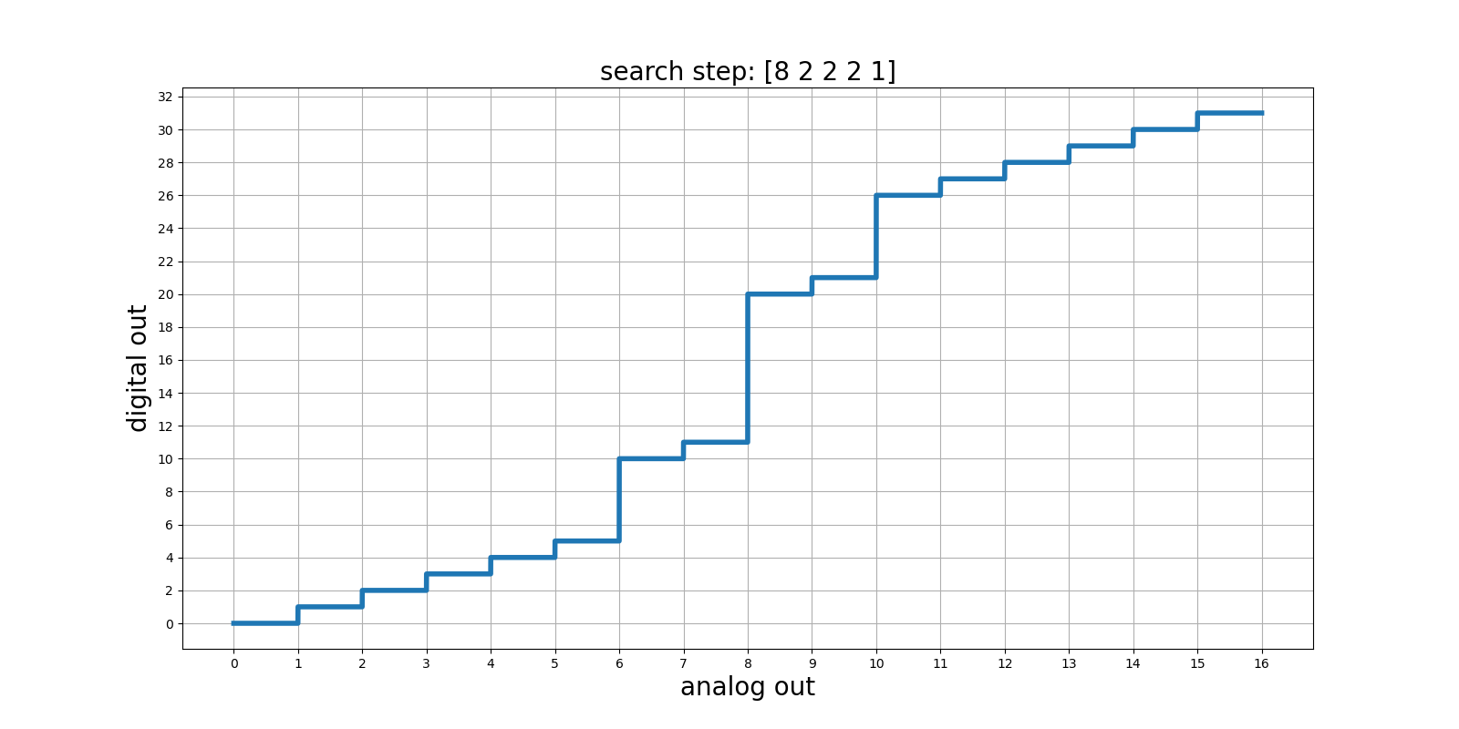
1 | import numpy as np |
ENOB vs. fixed radix
When the ADC is designed with a fixed radix, \(\alpha\) and the required number of conversion steps, \(M\)
the sum of all the step sizes \(s_{tot}\) \[ s_{tot} = \sum_{k=0}^{M-1} s_0 \alpha^k = s_0\frac{\alpha^M-1}{\alpha-1} \]
where \(s(i)\) is step size and \(i \in [0, 1, 2, M-1]\)
The effective number of bits, \(N\), can be calculated \[ N \leq \log 2\left(\frac{s_{tot} + s_0}{s_0}\right) = \frac{\alpha^M+\alpha-2}{\alpha-1} \]
Speed Benefit
TODO 📅
MSB with noise simualtion
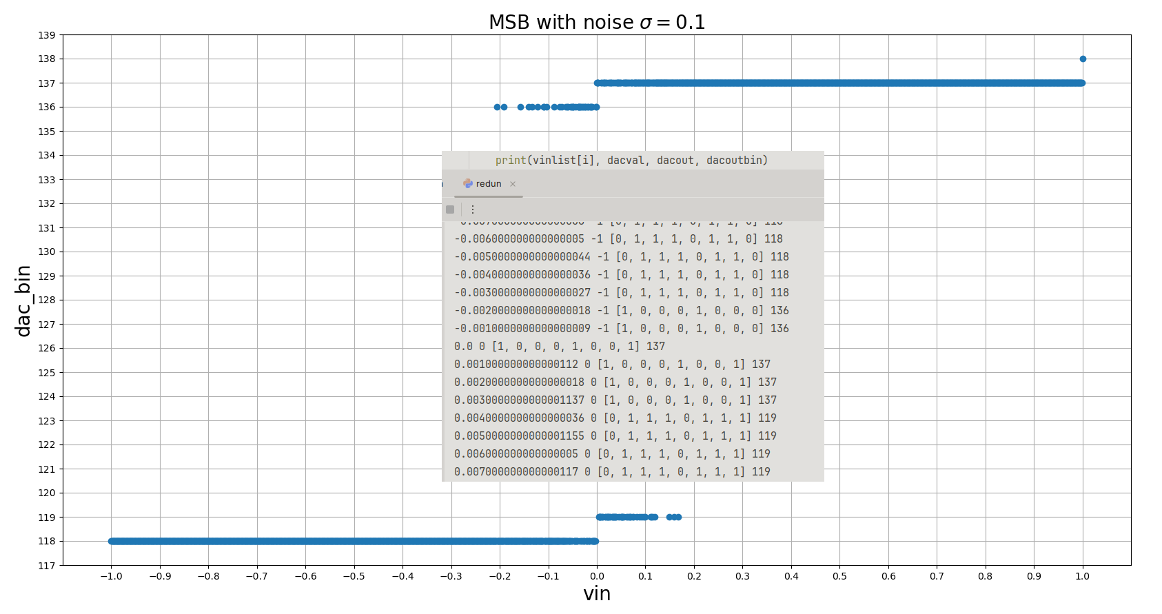
1 | import numpy as np |
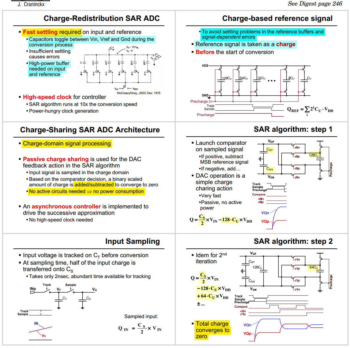
Charge-Sharing SAR ADC
J. Craninckx and G. van der Plas, "A 65fJ/Conversion-Step 0-to-50MS/s 0-to-0.7mW 9b Charge-Sharing SAR ADC in 90nm Digital CMOS," 2007 IEEE International Solid-State Circuits Conference. Digest of Technical Papers, San Francisco, CA, USA, 2007, pp. 246-600 [https://sci-hub.jp/10.1109/ISSCC.2007.373386]
V. Giannini, P. Nuzzo, V. Chironi, A. Baschirotto, G. Van der Plas and J. Craninckx, "An 820μW 9b 40MS/s Noise-Tolerant Dynamic-SAR ADC in 90nm Digital CMOS," 2008 IEEE International Solid-State Circuits Conference - Digest of Technical Papers, San Francisco, CA, USA, 2008, pp. 238-610 [https://sci-hub.jp/10.1109/ISSCC.2008.4523145]
Rabuske, Taimur & Fernandes, Jorge. (2016). Charge-Sharing SAR ADCs for Low-Voltage Low-Power Applications. 10.1007/978-3-319-39624-8.
Charge-based reference signal
- The trick is to analyze it in the charge domain rather than the voltage domain
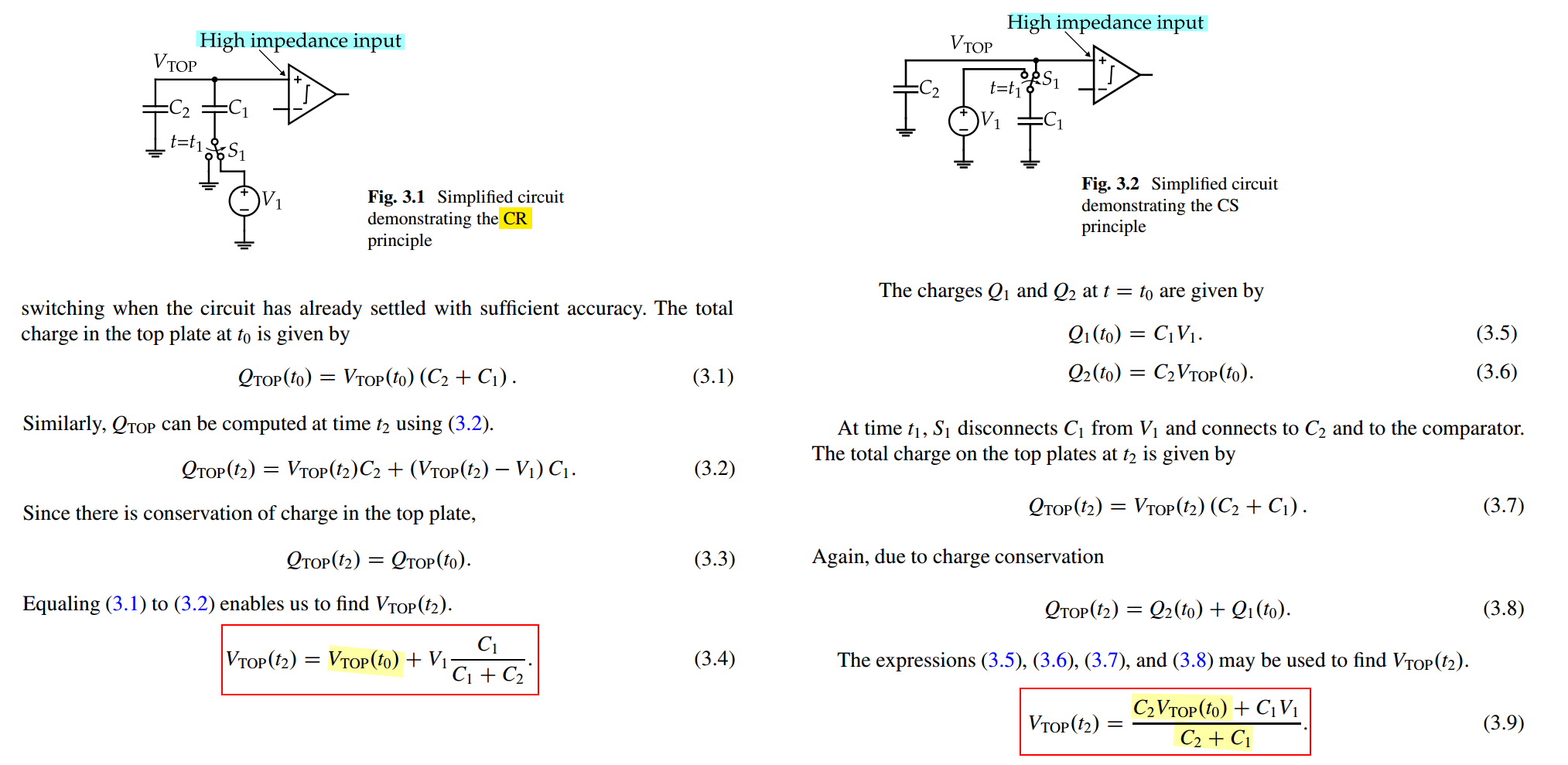
polarity switching in charge-sharing SAR capacitor arrays
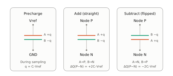
Each DAC capacitor C_i has two plates, A and B, and typically six switches:
- Two precharge switches: A to Vref and B to GND, closed during the sampling phase.
- Two "straight" switches: A to P and B to N.
- Two "crossed" switches: A to N and B to P

With \(C_A = C_B = C_s\) and \(\Delta V_C = V_{CP} - V_{CN}\): \[\begin{align} Q_A' &= V_A C_s + \Delta V_C \cdot C_C = V_A' C_s + (V_A' - V_B')C_C \\ Q_B' &= V_B C_s - \Delta V_C \cdot C_C = V_B' C_s - (V_A' - V_B')C_C \end{align}\] then \[ V_A' - V_B' = \frac{\textcolor{red}{C_s}\,(V_A - V_B) + \textcolor{red}{2C_C}\,\Delta V_C}{C_s + 2C_C} \qquad \frac{V_A' + V_B'}{2} = \frac{V_A + V_B}{2} \] This confirms the earlier claim: a floating capacitor \(C_C\) across \(P\) and \(N\) acts like \(2C_C\) in the single-ended picture. A straight connection has \(\Delta V_C = +V_\text{ref}\) (add), and a flipped connection has \(\Delta V_C = -V_\text{ref}\)
An ideal floating capacitor injects zero common-mode charge
| Aspect | Charge redistribution | Charge sharing |
|---|---|---|
| Reference during bit cycles | Connected, must settle each cycle | Disconnected, only precharges during sampling |
| Reference current | Signal-dependent | Constant (≈ C_DAC·Vref per conversion) |
| Reference buffer demand | High, especially at high fs | Relaxed; a large decoupling cap often suffices |
| Signal at comparator | Full swing | Attenuated by C_s / (C_s + C_DAC + C_p) |
| Full-scale / gain | Set by Vref | Set by Vref × capacitor ratio, sensitive to parasitics |
| Leakage sensitivity | Low | Higher, since precharged caps float during conversion |
| Typical resolution | Up to 16–18 bit | Usually ≤ 10–11 bit |
reference
Andrea Baschirotto, ISSCC2009 T6: SAR ADCs
Pieter Harpe, ISSCC 2016 Tutorial: "Basics of SAR ADCs Circuits & Architectures"
Yun Chiu, ISSCC2023 T3: "Fundamentals of Data Converters" [https://personal.utdallas.edu/~yxc101000/courses/7327/handout/isscc2023_tutorial.pdf]
Youngcheol Chae, Yonsei University, ISSCC 2023 F5.2 Design Techniques for Energy Efficient Analog-to-Digital Converters
Zhang, Milin, Zhihua Wang, Jan van der Spiegel and Franco Maloberti. "Advanced Tutorial on Analog Circuit Design." (2023)
Harpe, P. J. A. (2022). Low-Power SAR ADCs: Basic Techniques and Trends. IEEE Open Journal of the SolidState Circuits Society, 2, 73-81. Article 9908164 [https://ieeexplore.ieee.org/stamp/stamp.jsp?tp=&arnumber=9908164]
L. Jie et al., "An Overview of Noise-Shaping SAR ADC: From Fundamentals to the Frontier," in IEEE Open Journal of the Solid-State Circuits Society, vol. 1, pp. 149-161, 2021 [pdf]
Andrew Yu. Understanding Metastability in SAR ADCs: Part II: Asynchronous [https://github.com/phonon/sar-adc-metastability] [pdf]