ADC Characterization & Calibration
Figures of Merit (FoMs)
B. Murmann, "ADC Performance Survey 1997-2022," [Online]. Available: [https://github.com/bmurmann/ADC-survey]
Carsten Wulff, "Advanced Integrated Circuits 2025" [http://analogicus.com/aic2025/2025/02/20/Lecture-6-Oversampling-and-Sigma-Delta-ADCs.html#high-resolution-fom]

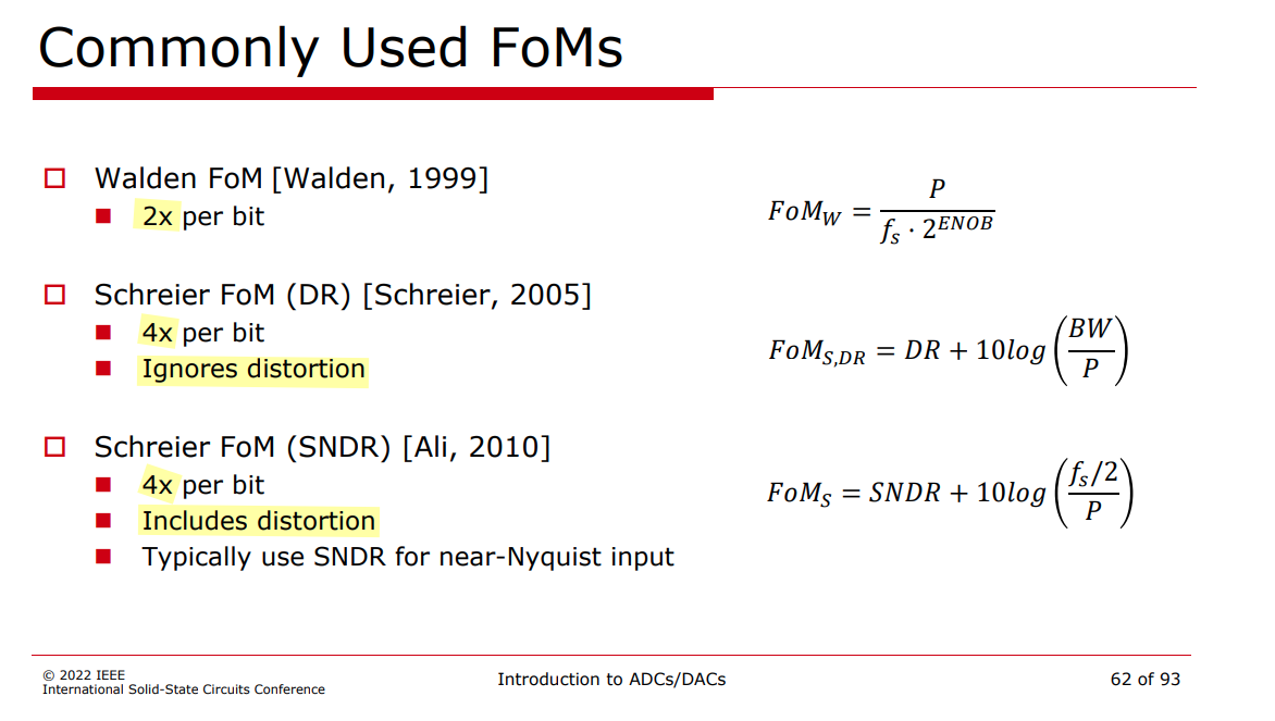
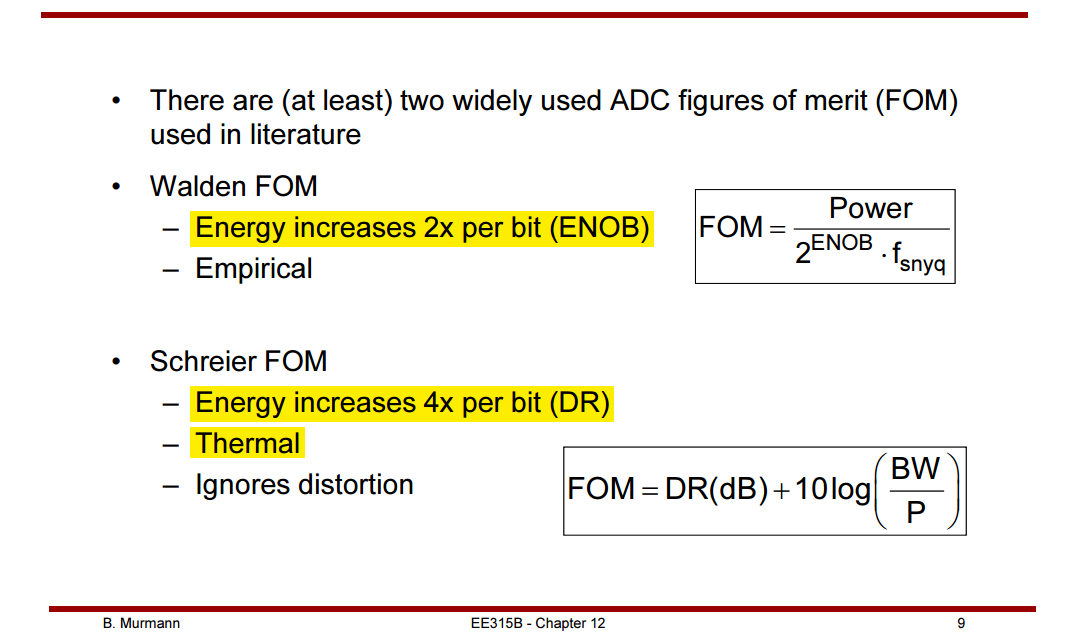
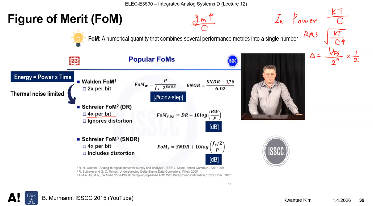
Walden FoM unit: J/conv-step [joules per conversion]
"Conversion-step" in the Walden FoM doesn't mean a physical operation like a comparator decision or a clock cycle. It means one quantization level, i.e., one effective LSB step out of the 2ENOB levels the converter can distinguish
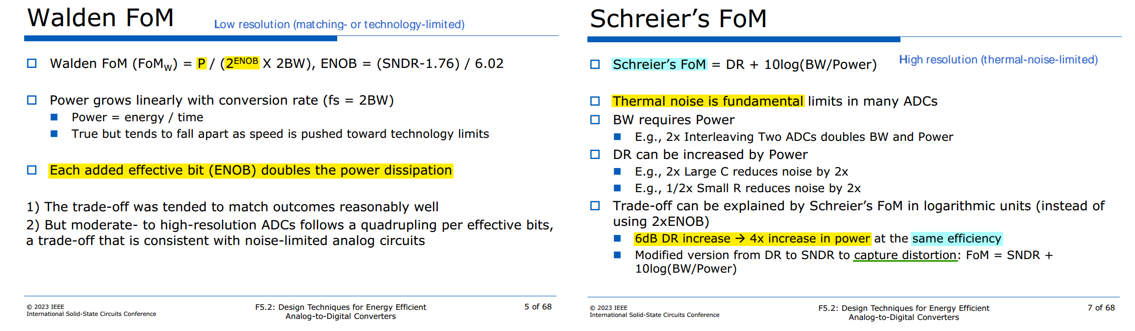
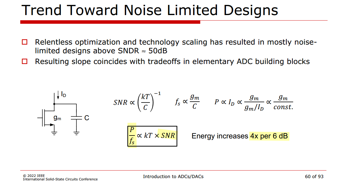
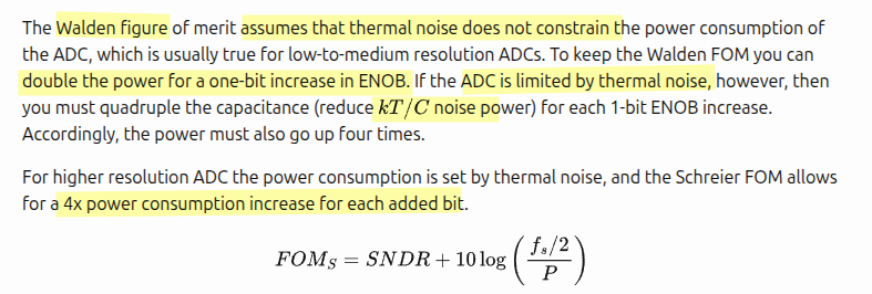
For Scherier FoM (DR, SNDR)

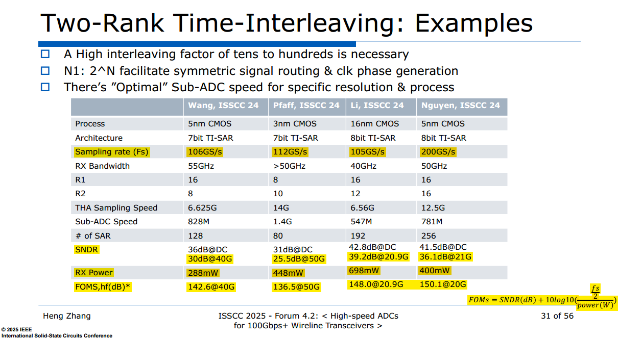
| Wang, ISSCC 24 | Pfaff, ISSCC 24 | Li, ISSCC 24 | Nguyen, ISSCC 24 | |
|---|---|---|---|---|
| Sampling rate (Fs) Gs/s | 106 | 112 | 105 | 200 |
| SNDR, hf (dB) | 30 | 25.5 | 39.2 | 36.1 |
| RX Power | 288 | 448 | 698 | 400 |
| FOM,hf (dB) | 82.6 | 76.5 | 88.0 | 90.1 |
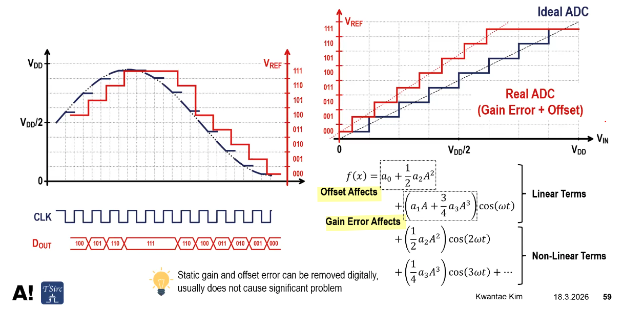
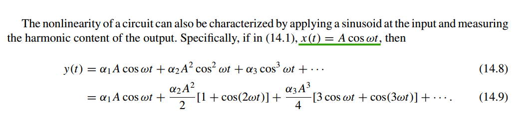
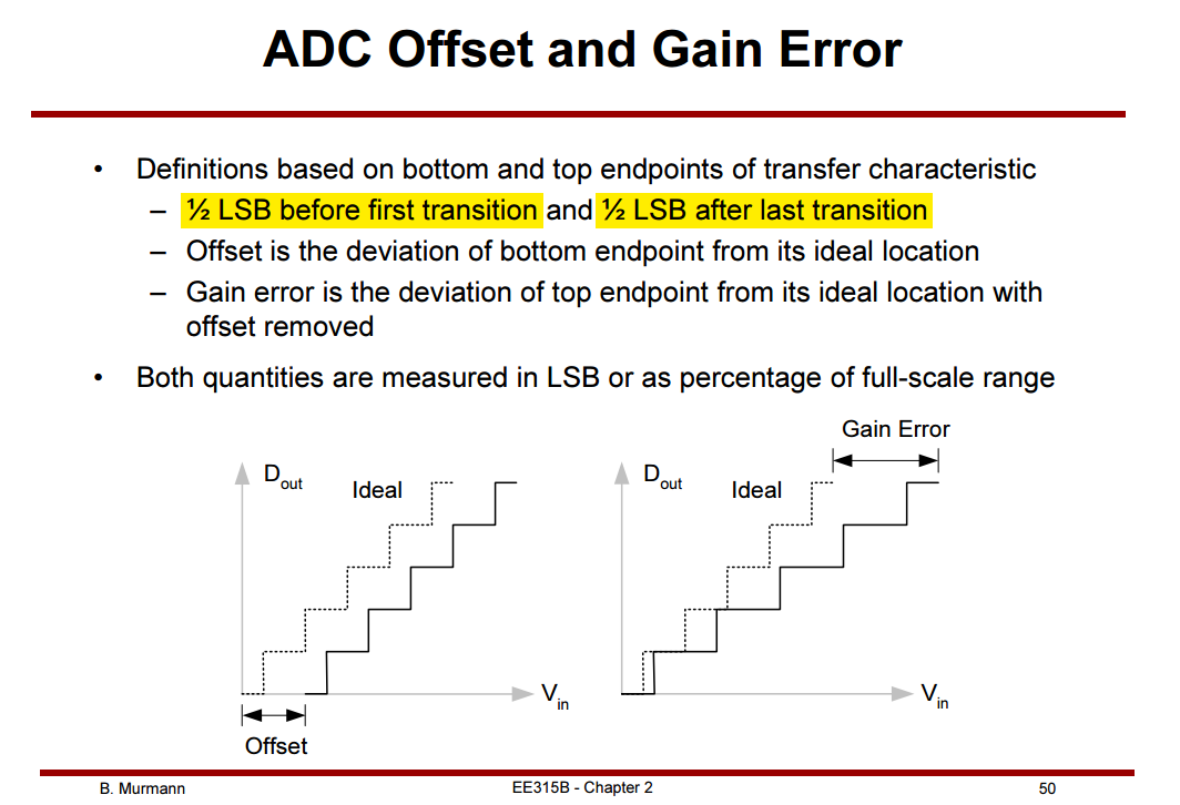
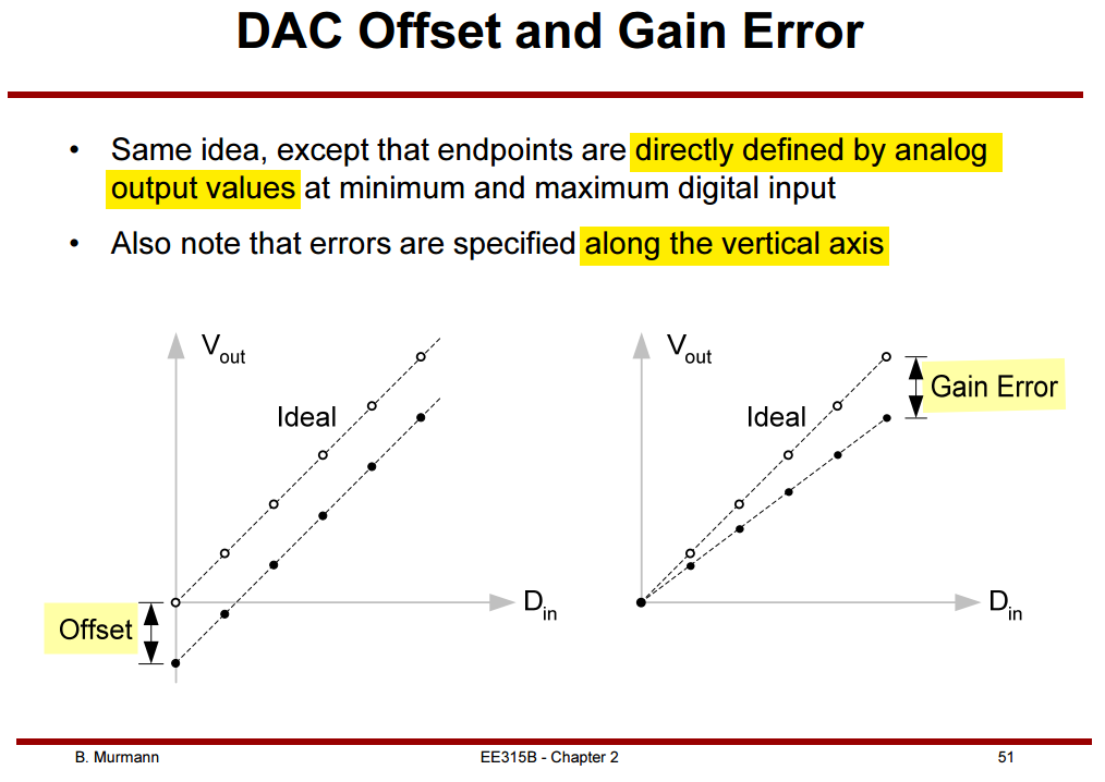
Offset & Gain Error
Kwantae Kim, Integrated Analog Systems D - Lecture 10 (ADC) [https://youtu.be/IEdbLNJb9wQ]
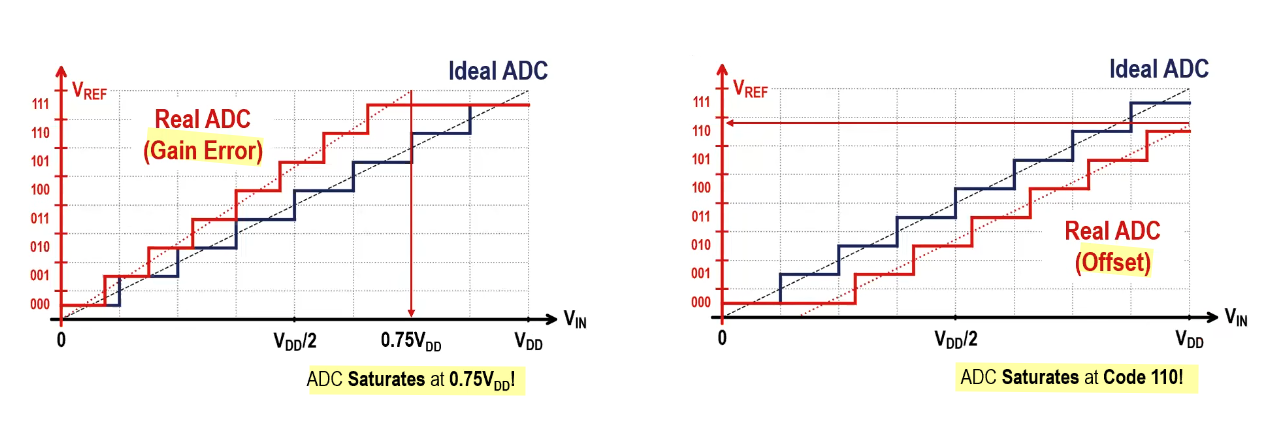
Offset Calibration
measured in digital domain: long-term averages of ADC out
If the input has a nonzero mean, the output average also contains the signal’s DC component, so it does not identify offset alone
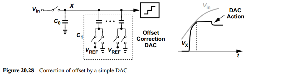
corrected in analog domain: ADC dynamic range reduction due to the offset, which holds if we force the offset of each channel to zero rather than make the offsets of different channels equal

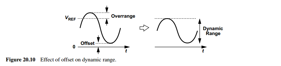
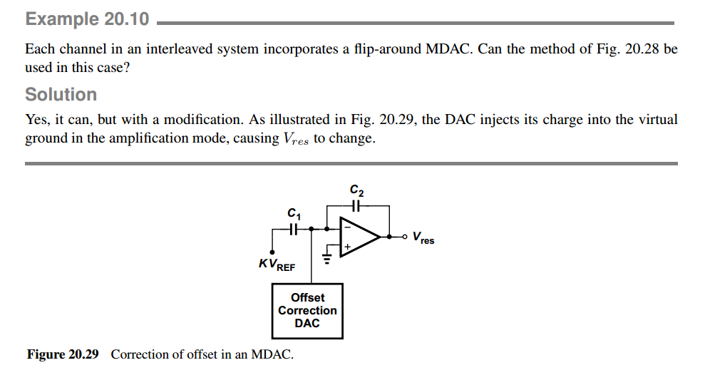
The offset-correction DAC here is a switched-capacitor DAC. Its digital code selects which capacitor bottom plates switch between ground and \(V_{\mathrm{REF}}\)
The op-amp holds the summing node approximately at virtual ground. The injected charge is balanced through feedback capacitor \(C_2\), causing \(V_{\mathrm{res}}\) to change.
For an ideal op-amp, the correction-induced output step is
\[ \boxed{\Delta V_{\mathrm{res}} =-\frac{\sum_k C_{D,k}\,\Delta V_{b,k}}{C_2}} \]
where \(C_{D,k}\) are the correction-DAC capacitors and \(\Delta V_{b,k}\) are their bottom-plate voltage changes.
Thus, the DAC supplies a digitally controlled charge correction, which the MDAC converts into an output-voltage correction.
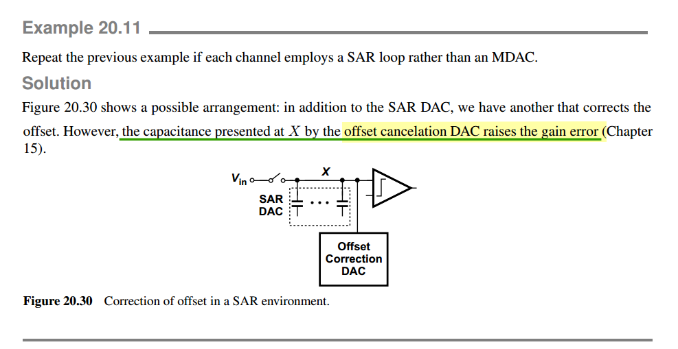
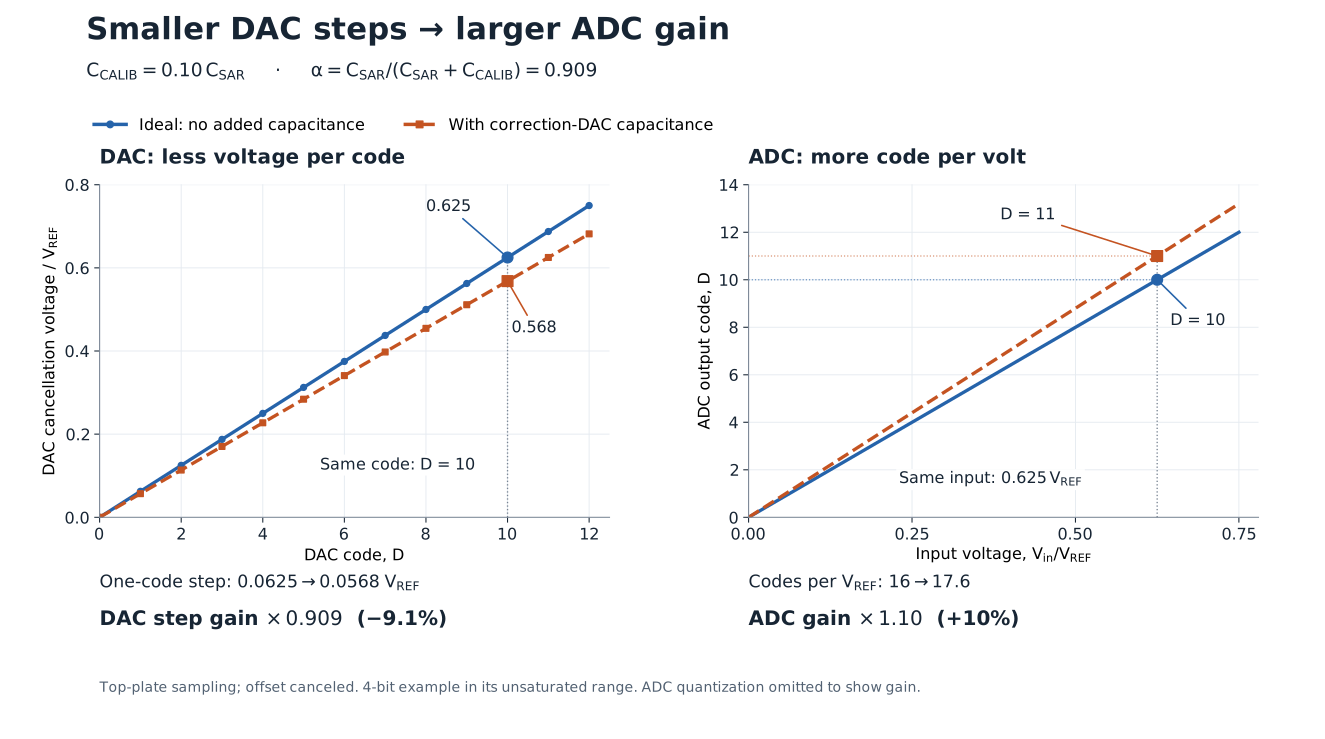
The correction DAC's bottom plates remain fixed during these trials, but its capacitance still loads \(X\)
neglecting other parasitic capacitances:
\[ G_{Q\rightarrow V,\mathrm{ideal}}=\frac{1}{C_{\mathrm{SAR}}}, \qquad \boxed{G_{Q\rightarrow V,\mathrm{loaded}} =\frac{1}{C_{\mathrm{SAR}}+C_{\mathrm{CALIB}}}} \]
During a SAR bit trial, switching capacitor \(C_k\) by \(\Delta V_{b,k}\) therefore produces
\[ \Delta V_X=\frac{C_k\,\Delta V_{b,k}} {C_{\mathrm{SAR}}+C_{\mathrm{CALIB}}} \]
Every SAR DAC voltage step is reduced by
\[ \boxed{\alpha=\frac{C_{\mathrm{SAR}}} {C_{\mathrm{SAR}}+C_{\mathrm{CALIB}}}<1} \]
the SAR DAC gain decreases, whereas the ADC’s output-code-per-volt gain increases. In the shown circuit, the sampling switch directly sets \(V_X=V_{\mathrm{in}}\), so the sampled input is not attenuated. Smaller DAC steps mean more code is needed to balance the same input: \[ \boxed{\frac{G_{\mathrm{ADC}}}{G_{\mathrm{ADC,ideal}}} =\frac{1}{\alpha} =1+\frac{C_{\mathrm{CALIB}}}{C_{\mathrm{SAR}}}} \]
Phase Calibration
Testing
Kent H. Lundberg "Analog-to-Digital Converter Testing" [https://www.mit.edu/~klund/A2Dtesting.pdf]
Tai-Haur Kuo, Da-Huei Lee "Analog IC Design: ADC Measurement" [http://msic.ee.ncku.edu.tw/course/aic/202309/ch13%20(20230111).pdf] [http://msic.ee.ncku.edu.tw/course/aic/aic.html]
ESE 6680: Mixed Signal Design and Modeling "Lec 20: April 10, 2023 Data Converter Testing" [https://www.seas.upenn.edu/~ese6680/spring2023/handouts/lec20.pdf]
Degang Chen. "Distortion Analysis" [https://class.ece.iastate.edu/djchen/ee435/2017/Lecture25.pdf]
TODO 📅
ADCToolbox
L. Jie and Z. Zhang. ADCToolbox [https://github.com/Arcadia-1/ADCToolbox]
SNR vs NSD — full-scale noise spread over the Nyquist band
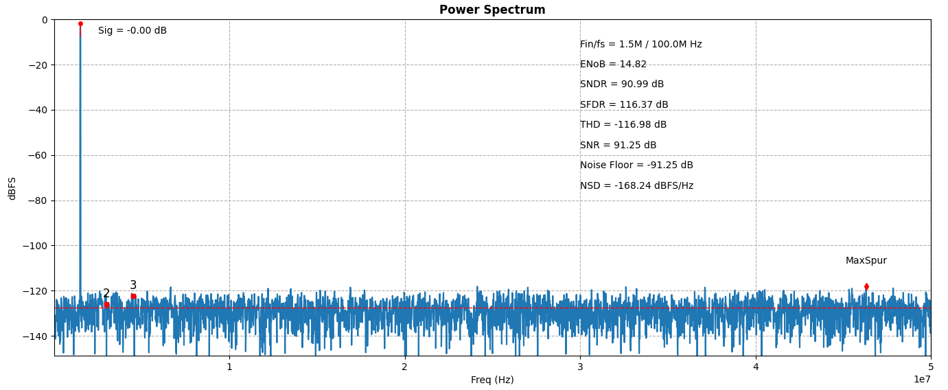
1 | ## https://github.com/Arcadia-1/ADCToolbox/blob/main/python/src/adctoolbox/examples/02_spectrum/exp_s01_analyze_spectrum_simplest.py |
reference
Aaron Buchwald, ISSCC2010 T1: "Specifying & Testing ADCs"
Ahmed M. A. Ali. ISSCC2021 T5: Calibration Techniques in ADCs
Boris Murmann, ISSCC2022 SC1: Introduction to ADCs/DACs: Metrics, Topologies, Trade Space, and Applications
—, ISSCC2012 SC3: Introduction to ADCs/DACs: Metrics, Topologies, Trade Space, and Applications
—, A/D Converter Figures of Merit and Performance Trends
Youngcheol Chae, Yonsei University, ISSCC 2023 F5.2 Design Techniques for Energy Efficient Analog-to-Digital Converters