Analog Techniques
Push-Pull
TODO 📅
Rinaldo Castello, "LINEARIZATION TECHNIQUES FOR PUSH-PULL AMPLIFIERS" [https://www.ieeetoronto.ca/wp-content/uploads/2020/06/AMPLIFIERS_Stanf_Tor_2016_Last.pdf]
Rail-to-Rail Op amp
[https://mixsignal.wordpress.com/wp-content/uploads/2013/03/689-604rail2rail.pdf]
TODO 📅
self-biased active loading

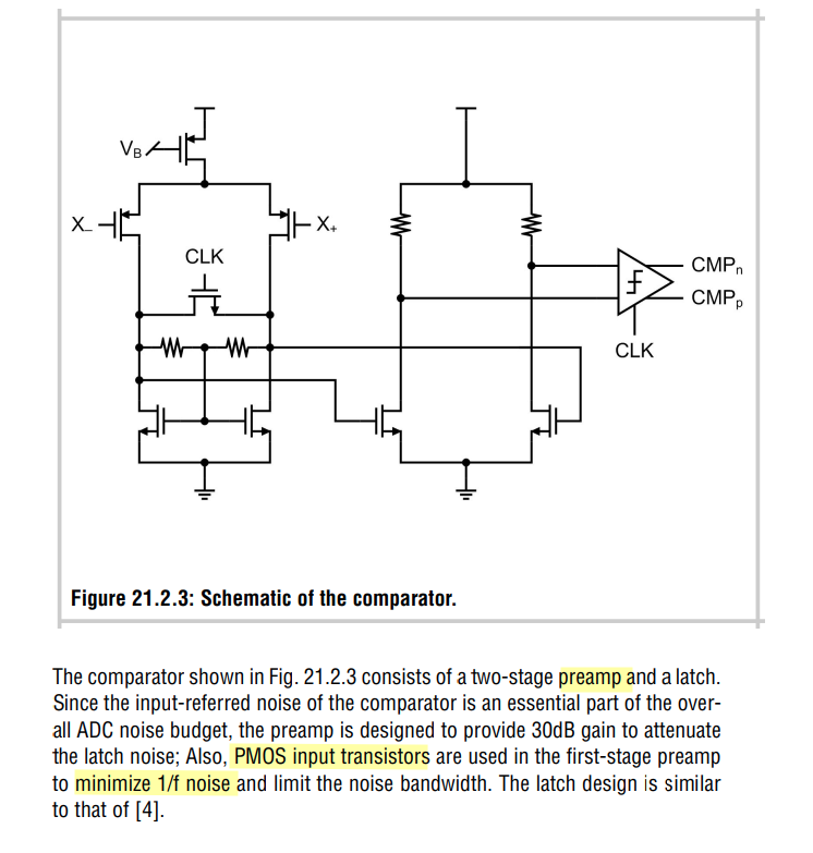
Vishal Saxena "CMOS Comparator Design Extra Slides" [https://www.eecis.udel.edu/~vsaxena/courses/ece614/Handouts/Comparator%20Slides.pdf]

W. Liu, P. Huang and Y. Chiu, "A 12b 22.5/45MS/s 3.0mW 0.059mm2 CMOS SAR ADC achieving over 90dB SFDR," 2010 IEEE International Solid-State Circuits Conference - (ISSCC), San Francisco, CA, USA, 2010 [https://sci-hub.se/10.1109/ISSCC.2010.5433830]
Slewing in Folded-Cascode Op Amps
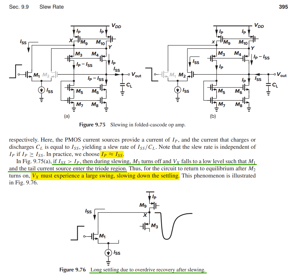
In practice, we choose \(I_P \simeq I_{SS}\)
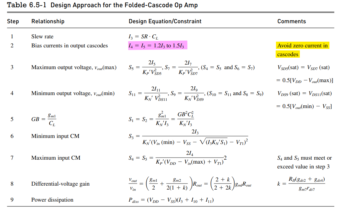
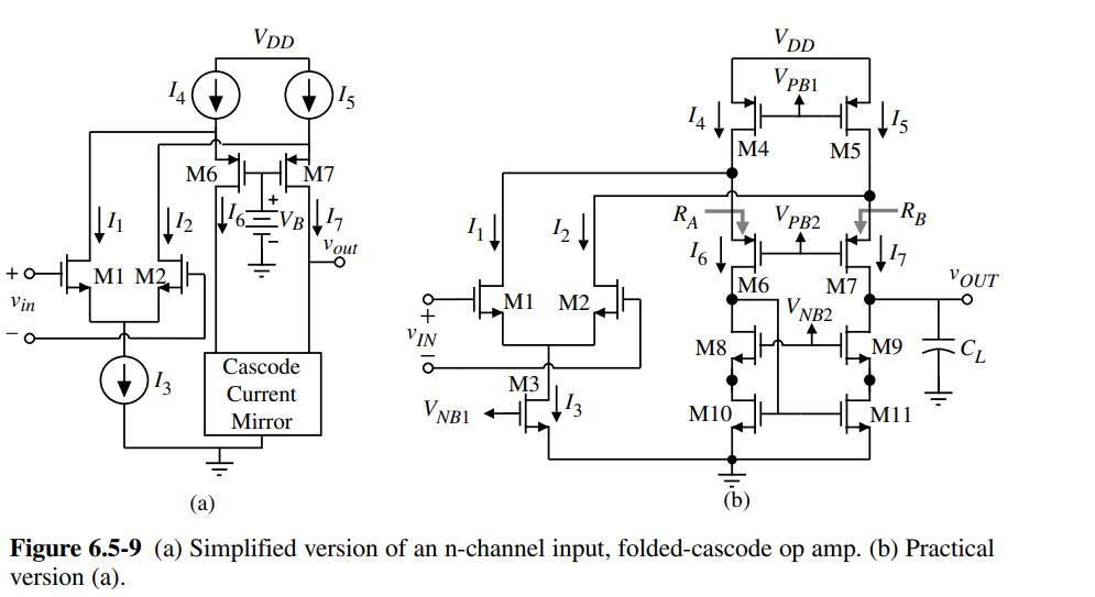
Avoid zero current in cascodes
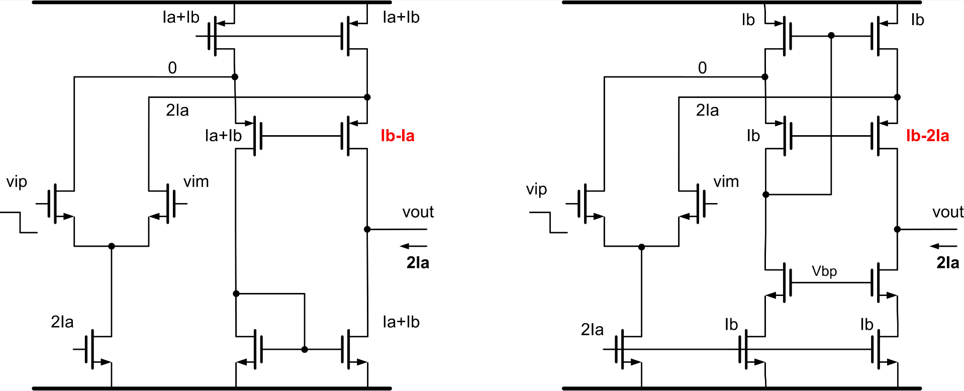
left circuit
\(I_b \gt I_a\)
right circuit
\(I_b \gt 2I_a\)
Huijsing, J. H. (2017). Operational Amplifiers: Theory and Design. (3 ed.) Springer
[https://bbs.eetop.cn/forum.php?mod=redirect&goto=findpost&ptid=995502&pid=11548528]
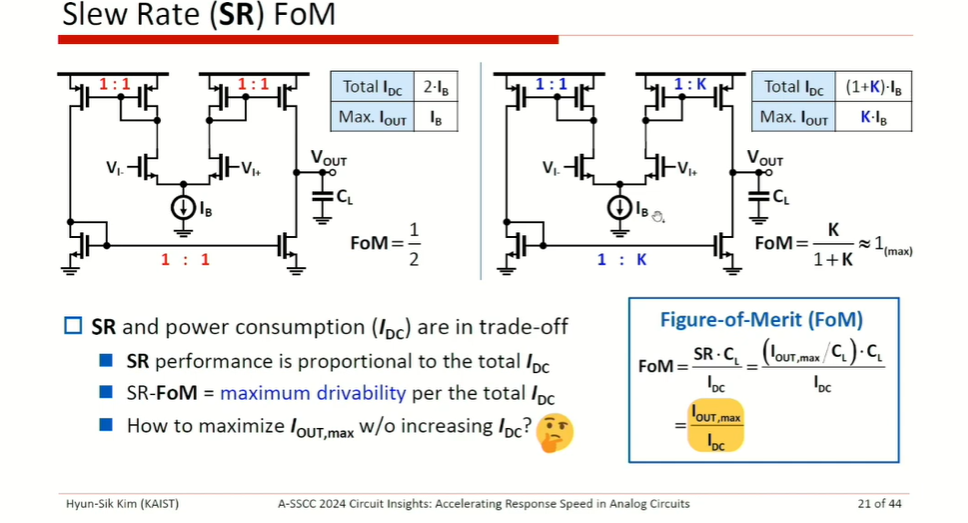
Response Speed in Analog Circuits
Hyun-Sik Kim, KAIST, A-SSCC 2024 Circuit Insights: FT3 Accelerating Response Speed in Analog Circuits [link]
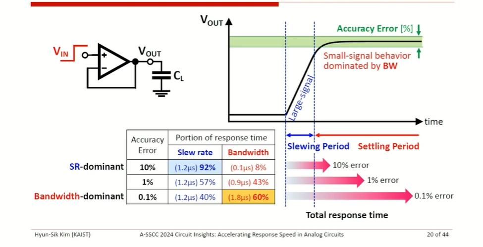
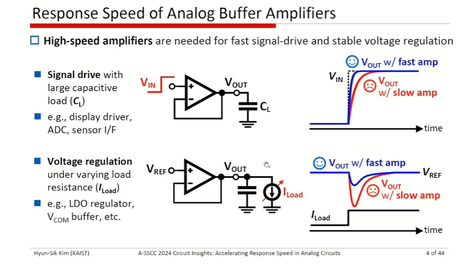
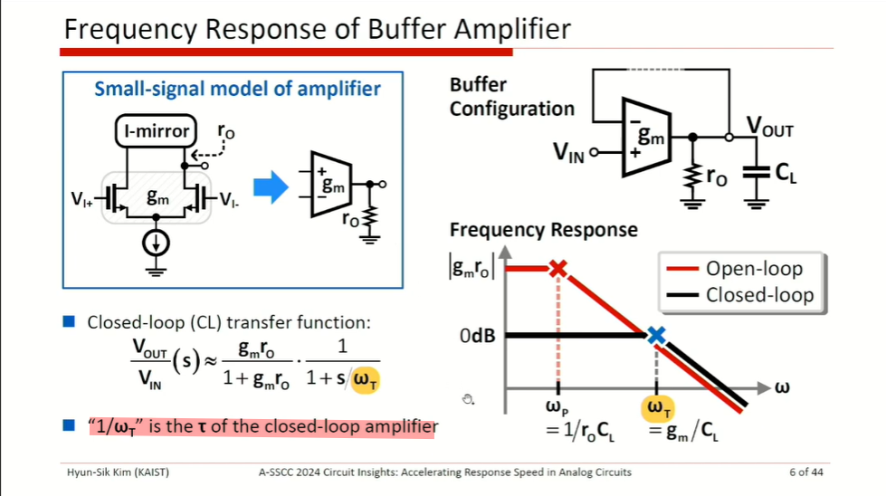
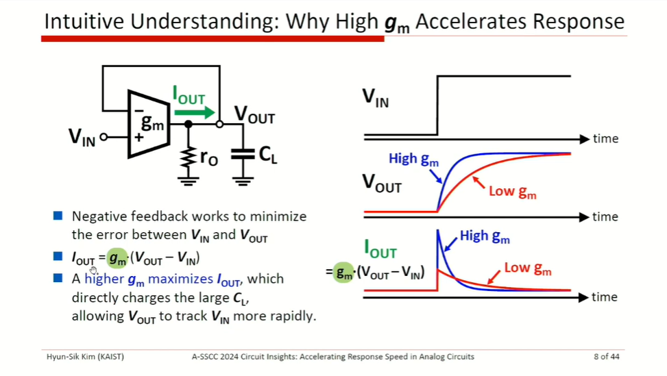
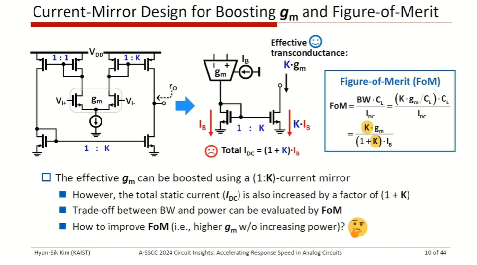
Bandwidth limitation

slew rate limitation
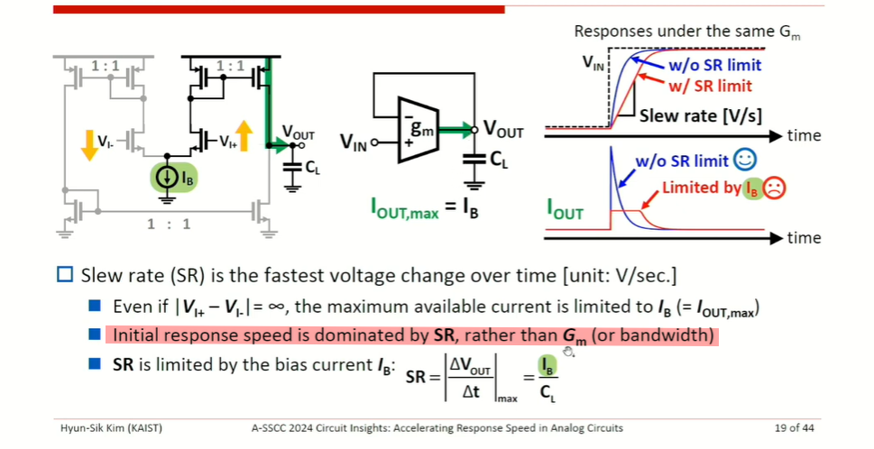
Assuming linear response \[ V_o(t) = 1 - e^{-\omega_T t} \]
\[ \frac{dV_o}{dt} = \omega_Te^{-\omega_T t} = \frac{g_m}{C_L}e^{-\omega_T t} = \frac{g_m}{I_B}\cdot \frac{I_B}{C_L}\cdot e^{-\omega_T t} \gt \frac{I_B}{C_L} \]
where \(\frac{g_m}{I_B} e^{-\omega_T t} \gt 1\) at initial response
Therefore, initial response speed is dominated by SR, rather than \(G_m\) (or bandwidth)
MOS parasitic Rd&Rs, Cd&Cs
Decrease the parasitic R&C
priority: \(R_s \gt R_d\), \(C_s \gt C_d\)
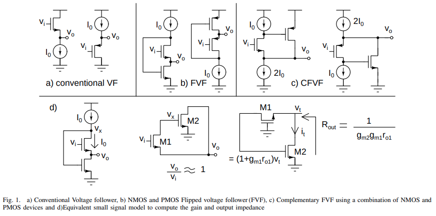
source follower
A. Sheikholeslami, "Voltage Follower, Part III [Circuit Intuitions]," in IEEE Solid-State Circuits Magazine, vol. 15, no. 2, pp. 14-26, Spring 2023, doi: 10.1109/MSSC.2023.3269457
—, ESSCIRC2023 Circuit Insights [https://youtu.be/2xFIZM5_FPw]
—, CICC2025 Circuit Insights: From Simple to Super Source Follower [https://youtu.be/CWfMKltPIQ8]
Paul R. Gray. 2009. Analysis and Design of Analog Integrated Circuits (5th. ed.). Wiley Publishing. [pdf]
Super-source follower (SSF)
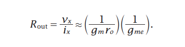
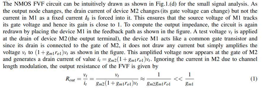
Flipped Voltage Follower (FVF)
T&H buffer in ADC
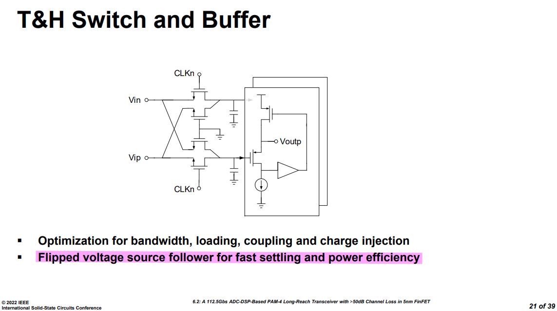
Z. Guo et al., "A 112.5Gb/s ADC-DSP-Based PAM-4 Long-Reach Transceiver with >50dB Channel Loss in 5nm FinFET," 2022 IEEE International Solid-State Circuits Conference (ISSCC), San Francisco, CA, USA, 2022, pp. 116-118, doi: 10.1109/ISSCC42614.2022.9731650.
Double Differential pair
\(V_\text{ip}\) and \(V_\text{im}\) are input, \(V_\text{rp}\) and \(V_\text{rm}\) are reference voltage \[ V_o = A_v(\overline{V_\text{ip} - V_\text{im}} - \overline{V_\text{rp} - V_\text{rm}}) \]

In differential comparison mode, the feedback loop ensure \(V_\text{ip} = V_\text{rp}\), \(V_\text{im} = V_\text{rm}\) in the end
assume input and reference common voltage are same
Pros of (b)
- larger input range i.e., \(\gt \pm \sqrt{2}V_\text{ov}\) of (a), it works even one differential is off due to lower voltage
- larger \(g_m\) (smaller input difference of pair)
Cons of (b)
- sensitive to the difference of common voltage between \(V_\text{ip}\), \(V_\text{im}\) and \(V_\text{rp}\), \(V_\text{rm}\)
common-mode voltage difference

copy aforementioned formula here for convenience \[ V_o = A_v(\overline{V_\text{ip} - V_\text{im}} - \overline{V_\text{rp} - V_\text{rm}}) \]
at sample phase \(V_\text{ip}= V_\text{im}= V_\text{cmi}\) and \(V_\text{rp}= V_\text{rm}= V_\text{cmr}\)
- \(I_\text{ip0}= I_\text{im0} = I_\text{i0}\)
- \(I_\text{rp0}= I_\text{rm0} = I_\text{r0}\)
i.e. \(\overline{I_\text{ip} + I_\text{rm}} - \overline{I_\text{im} + I_\text{rp}} = 0\)
at compare start
\(V_\text{ip}= V_\text{im}= V_\text{cmi}\) and \(V_\text{rp}= V_\text{cmr}+\Delta\), \(V_\text{rp}= V_\text{cmr}-\Delta\)
\(I_\text{ip}\lt I_\text{ip0}\), \(I_\text{rp} \gt I_\text{rp0}\)
\(I_\text{im}\gt I_\text{im0}\), \(I_\text{rm} \lt I_\text{rm0}\)
i.e. \(\overline{I_\text{ip} + I_\text{rm}} - \overline{I_\text{im} + I_\text{rp}} \lt 0\), we need to increase \(V_\text{ip}\) and decrease \(V_\text{im}\).
at the compare finish
\[\begin{align} V_\text{ip}= V_\text{cmi} + \Delta \\ V_\text{im}= V_\text{cmi} - \Delta \end{align}\]
and \(I_\text{ip0}= I_\text{im0} = I_\text{i0}\), \(I_\text{rp0}= I_\text{rm0} = I_\text{r0}\)
i.e. \(\overline{I_\text{ip} + I_\text{rm}} - \overline{I_\text{im} + I_\text{rp}} = 0\)
If \(V_\text{cmr} - V_\text{cmi} = \sqrt{2}V_{OV} + \delta\), and \(\delta \gt 0\). one transistor carries the entire tail current
- \(I_\text{ip} =0\) and \(I_\text{rp} = I_{SS}\), all the time
At the end, \(V_\text{im} = V_\text{cmi} - (\Delta - \delta)\), the error is \(\delta\)
In closing, \(V_\text{cmr} - V_\text{cmi} \lt \sqrt{2}V_{OV}\) for normal work
Furthermore, the difference between \(V_\text{cmr}\) and \(V_\text{cmi}\) should be minimized due to limited impedance of current source and input pair offset
In the end \[ V_\text{cmr} - V_\text{cmi} \lt \sqrt{2}V_{OV} - V_{OS} \]
Under the condition, every transistor of pairs are on in equilibrium
pair mismatch

\[\begin{align} I_{SE} &= g_m(\sigma_{vth,0} + \sigma_{vth,1}) \\ I_{DE} &= g_m(\sigma_{vth,0} + \sigma_{vth,1}) \end{align}\]
The input equivalient offset voltage \[\begin{align} V_{os,SE} &= \frac{I_{SE}}{2g_m} = \frac{\sigma_{vth,0} + \sigma_{vth,1}}{2} \\ V_{os,DE} &= \frac{I_{DE}}{g_m} = \sigma_{vth,0} + \sigma_{vth,1} \end{align}\]
Then \[\begin{align} \sigma_{vos,SE} &= \sqrt{\frac{2\sigma_{vth}^2}{4}} = \frac{\sigma_{vth}}{\sqrt{2}} \\ \sigma_{vos,DE} &= \sqrt{2\sigma_{vth}^2} = \sqrt{2}\sigma_{vth} \end{align}\]
We obtain \[ \sigma_{vos,DE} = 2\sigma_{vos,SE} \]
Input Differential pair
Todd Brooks, Broadcom "Input Programmable Gain Amplifier (PGA) Design for ADC Signal Conditioning" [https://classes.engr.oregonstate.edu/eecs/spring2021/ece627/Lecture%20Notes/OSU%20Classroom%20Presentaton%20042511.ppt]
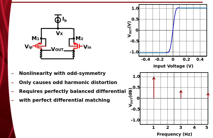
DM Distortion
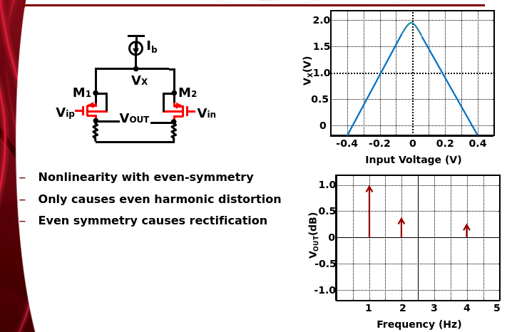
CM Distortion
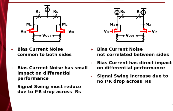
Resistive Degeneration
Resistive degeneration in differential pairs serves as one major technique for linear amplifier
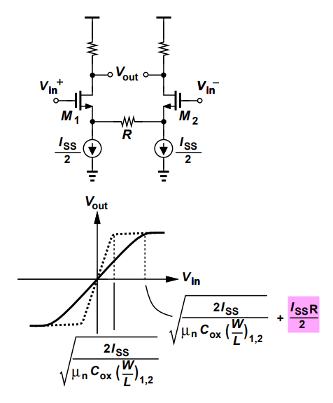
The linear region for CMOS differential pair would be extended by \(±I_{SS}R/2\) as all of \(I_{SS}/2\) flows through \(R\). \[\begin{align} V_{in}^+ -V_{in}^- &= V_{OV} + V_{TH}+\frac{I_{SS}}{2}R - V_{TH} \\ &= \sqrt{\frac{2I_{SS}}{\mu_nC_{OX}\frac{W}{L}}} + \frac{I_{SS}R}{2} \end{align}\]
Jri Lee, "Communication Integrated Circuits." https://cc.ee.ntu.edu.tw/~jrilee/publications/Comm_IC.pdf
Figure 14.12, Design of Analog CMOS Integrated Circuits, Second Edition [https://electrovolt.ir/wp-content/uploads/2014/08/Design-of-Analog-CMOS-Integrated-Circuit-2nd-Edition-ElectroVolt.ir_.pdf]
Biasing Tradeoffs in Resistive-Degenerated Diff Pair