Multi-phase Clock Generation
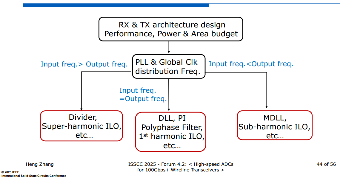
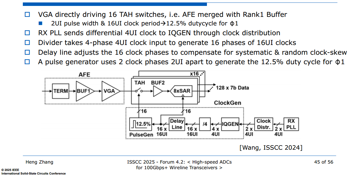
MPG using Divider
J. Q. Wang et al., "7.1 A 2.69pJ/b 212Gb/s DSP-Based PAM-4 Transceiver for Optical Direct-Detect Application in 5nm FinFET," 2024 IEEE International Solid-State Circuits Conference (ISSCC), San Francisco, CA, USA, 2024, pp. 123-125, doi: 10.1109/ISSCC49657.2024.10454275.
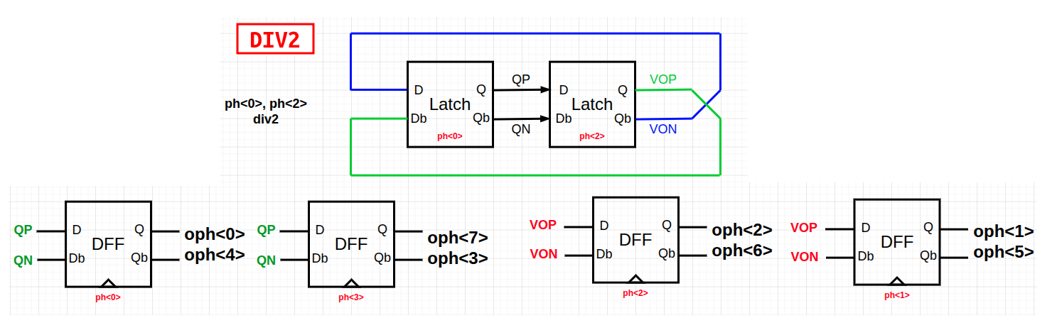
ph<0:3> 4UI clock to oph<0:15> 16UI clock
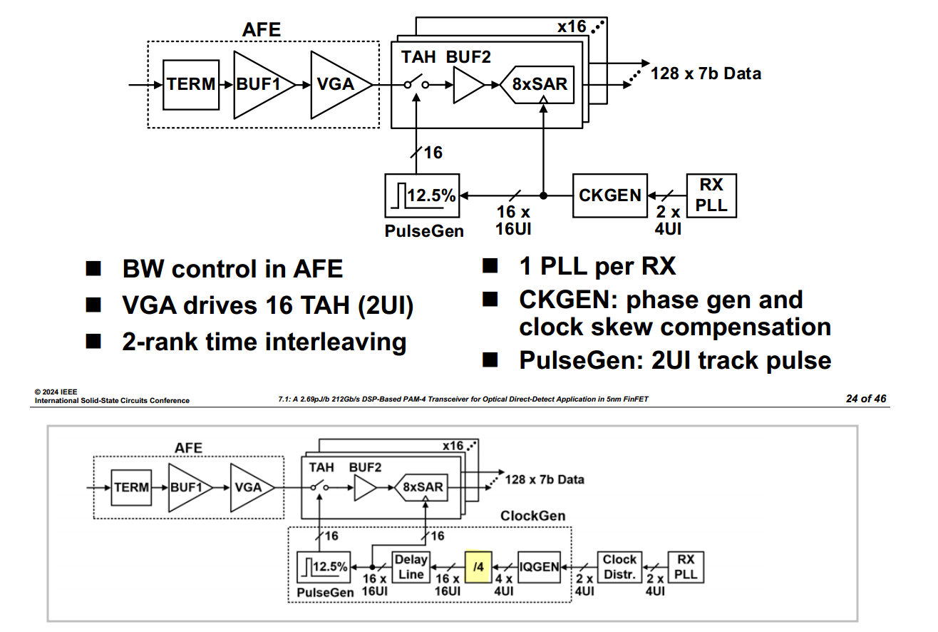


| D / Db | Retiming clock (rising edge) | Q | Qb |
|---|---|---|---|
| QP1 / QN1 | ph<0> | oph<4> | oph<12> |
| VOP1 / VON1 | ph<0> | oph<8> | oph<0> |
| QP2 / QN2 | ph<2> | oph<6> | oph<14> |
| VOP2 / VON2 | ph<2> | oph<10> | oph<2> |
| QP1 / QN1 | ph<3> | oph<3> | oph<11> |
| VOP1 / VON1 | ph<3> | oph<7> | oph<15> |
| QP2 / QN2 | ph<1> | oph<5> | oph<13> |
| VOP2 / VON2 | ph<1> | oph<9> | oph<1> |
ph<0:3> 4UI clock to oph<0:7> 8UI clock

MPG using ILO
D. Pfaff et al., "7.3 A 224Gb/s 3pJ/b 40dB Insertion Loss Transceiver in 3nm FinFET CMOS," 2024 IEEE International Solid-State Circuits Conference (ISSCC), San Francisco, CA, USA, 2024, pp. 128-130, doi: 10.1109/ISSCC49657.2024.10454537
Y. Tian et al., "A 28-nm 8–28-GHz Eight-Phase Clock Generator Using an Injection-Locked Dual-Feedback Ring Oscillator," in IEEE Journal of Solid-State Circuits, vol. 61, no. 1, pp. 47-62, Jan. 2026, doi: 10.1109/JSSC.2025.3613940
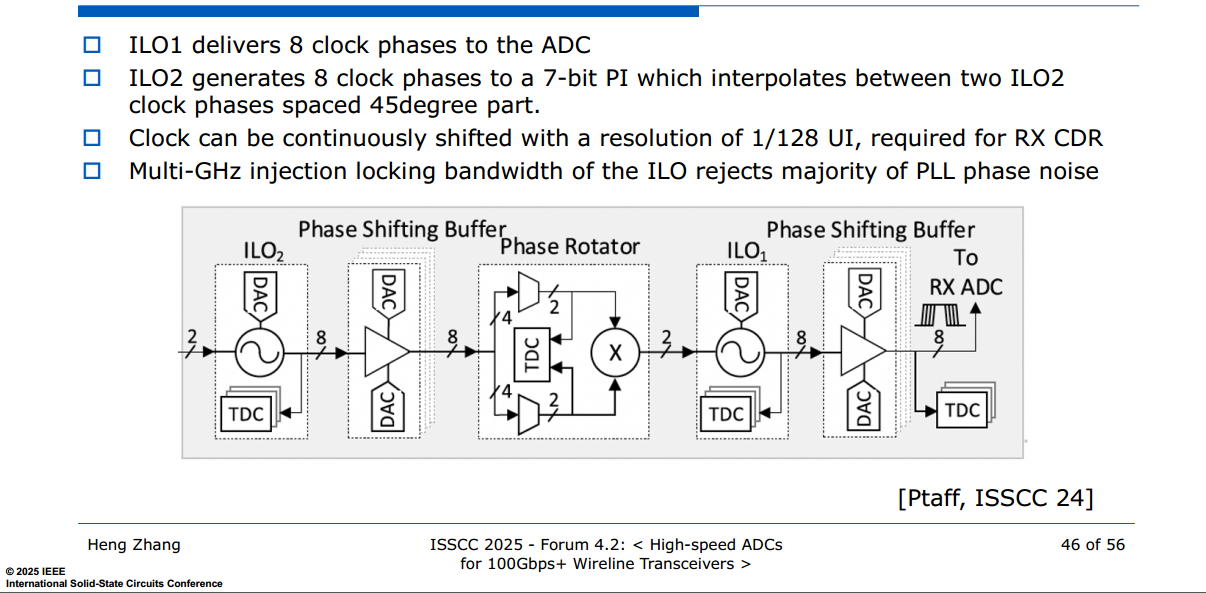
delay line based Skew Correction
D. Pfaff et al., "7.3 A 224Gb/s 3pJ/b 40dB Insertion Loss Transceiver in 3nm FinFET CMOS," 2024 IEEE International Solid-State Circuits Conference (ISSCC), San Francisco, CA, USA, 2024, pp. 128-130, doi: 10.1109/ISSCC49657.2024.10454537
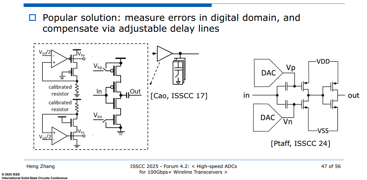
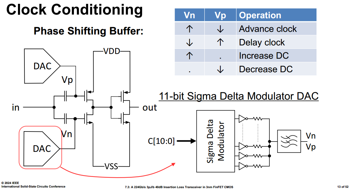
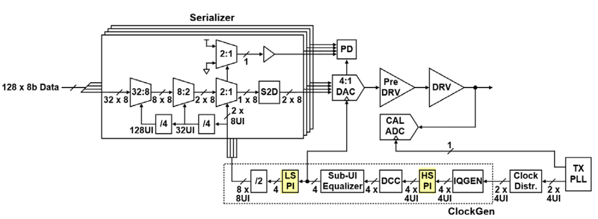
phase interpolator based Skew Correction
J. Q. Wang et al., "7.1 A 2.69pJ/b 212Gb/s DSP-Based PAM-4 Transceiver for Optical Direct-Detect Application in 5nm FinFET," 2024 IEEE International Solid-State Circuits Conference (ISSCC), San Francisco, CA, USA, 2024, pp. 123-125, doi: 10.1109/ISSCC49657.2024.10454275
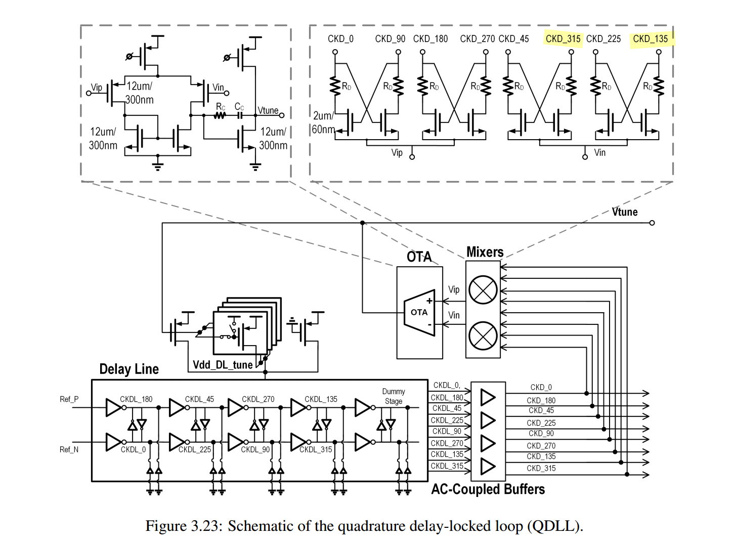
mixer based Quadrature Phase Detector
S. Chen et al., "A 4-to-16GHz inverter-based injection-locked quadrature clock generator with phase interpolators for multi-standard I/Os in 7nm FinFET," 2018 IEEE International Solid-State Circuits Conference - (ISSCC), San Francisco, CA, USA, 2018, pp. 390-39 [https://sci-hub.red/storage/twin/6715/2bc891863e9eac1eb1670deb776ff04d/chen2018.pdf]
Z. Wang, Y. Zhang, Y. Onizuka and P. R. Kinget, "11.4 A High-Accuracy Multi-Phase Injection-Locked 8-Phase 7GHz Clock Generator in 65nm with 7b Phase Interpolators for High-Speed Data Links," 2021 IEEE International Solid-State Circuits Conference (ISSCC), San Francisco, CA, USA, 2021, pp. 186-188, [https://sci-hub.ru/10.1109/ISSCC42613.2021.9365800]
—, "Multi-Phase Clock Generation for Phase Interpolation With a Multi-Phase, Injection-Locked Ring Oscillator and a Quadrature DLL," in IEEE Journal of Solid-State Circuits, vol. 57, no. 6, pp. 1776-1787, June 2022, doi: 10.1109/JSSC.2021.3124486.
—, "A Very High Linearity Twin Phase Interpolator With a Low-Noise and Wideband Delta Quadrature DLL for High-Speed Data Link Clocking," in IEEE Journal of Solid-State Circuits, vol. 58, no. 4, pp. 1172-1184, April 2023, doi: 10.1109/JSSC.2022.3197061
—. Efficient and High-Performance Clocking Circuits for High-Speed Data Links. 2022. Columbia University, PhD dissertation. Academic Commons,[https://academiccommons.columbia.edu/doi/10.7916/g3f1-4e71]
Shaokang ZHAO, 2025, "Multi-Phase Clock Generator for High-Speed Wireline Systems," [paper, slides]
J. Im et al., "A 112-Gb/s PAM-4 Long-Reach Wireline Transceiver Using a 36-Way Time-Interleaved SAR ADC and Inverter-Based RX Analog Front-End in 7-nm FinFET," in IEEE Journal of Solid-State Circuits, vol. 56, no. 1, pp. 7-18, Jan. 2021, [https://sci-hub.jp/10.1109/JSSC.2020.3024261]
 \[
V_{ip}=\mathrm{XNOR}(CKD_0,CKD_{90})\qquad \qquad
V_{in}=\mathrm{XNOR}(CKD_{45},CKD_{315})
\]
\[
V_{ip}=\mathrm{XNOR}(CKD_0,CKD_{90})\qquad \qquad
V_{in}=\mathrm{XNOR}(CKD_{45},CKD_{315})
\]
The \(225^\circ\) per-stage phase shift is constrained by the minimum inverter propagation delay
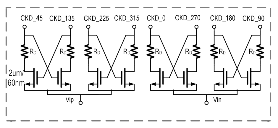
complementary of mixers-based QPD
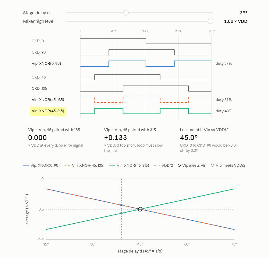
A natural approach is to compare
\[ \mathrm{XOR}(CKD_0,CKD_{90})+\mathrm{XOR}(CKD_{45},CKD_{135}) \]
against
\[ \mathrm{XNOR}(CKD_0,CKD_{90})+\mathrm{XNOR}(CKD_{45},CKD_{135}) \]
Its main limitation is that accurate phase detection relies on the input clocks having a 50% duty cycle.
calibration ADC based skew detection
J. Q. Wang et al., "7.1 A 2.69pJ/b 212Gb/s DSP-Based PAM-4 Transceiver for Optical Direct-Detect Application in 5nm FinFET," 2024 IEEE International Solid-State Circuits Conference (ISSCC), San Francisco, CA, USA, 2024, pp. 123-125, doi: 10.1109/ISSCC49657.2024.10454275.
TODO 📅
DCC & AC-coupled buffer
The amount of correction can be set by intentional injection of an offset current into the summing input node of INV, threshold-adjustable inverter
Note that the change to the threshold is opposite in direction to the change to INV
increasing DC of input signal is equivalent to lower down the threshold of INV
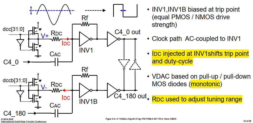
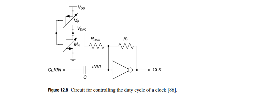
voltage at INV1 will increased by: \[ \frac{\Delta V_{DAC} - \Delta {INV1}}{R_{DAC}} = \frac{\Delta {INV1} +A_0 \Delta {INV1}}{R_{F}} \] therefore \[ \Delta {INV1} = \Delta V_{DAC} \cdot \frac{R_F}{R_F+(A_0+1)R_{DAC}} \approx \Delta V_{DAC} \cdot \frac{R_F}{A_0R_{DAC}} \]
variable \(R_{DAC}\) can be used to tweak tuning resolution & range
If \(R_{DAC} = R_F\) \[ \Delta {INV1}\approx \frac{\Delta V_{DAC}}{A_0} \]
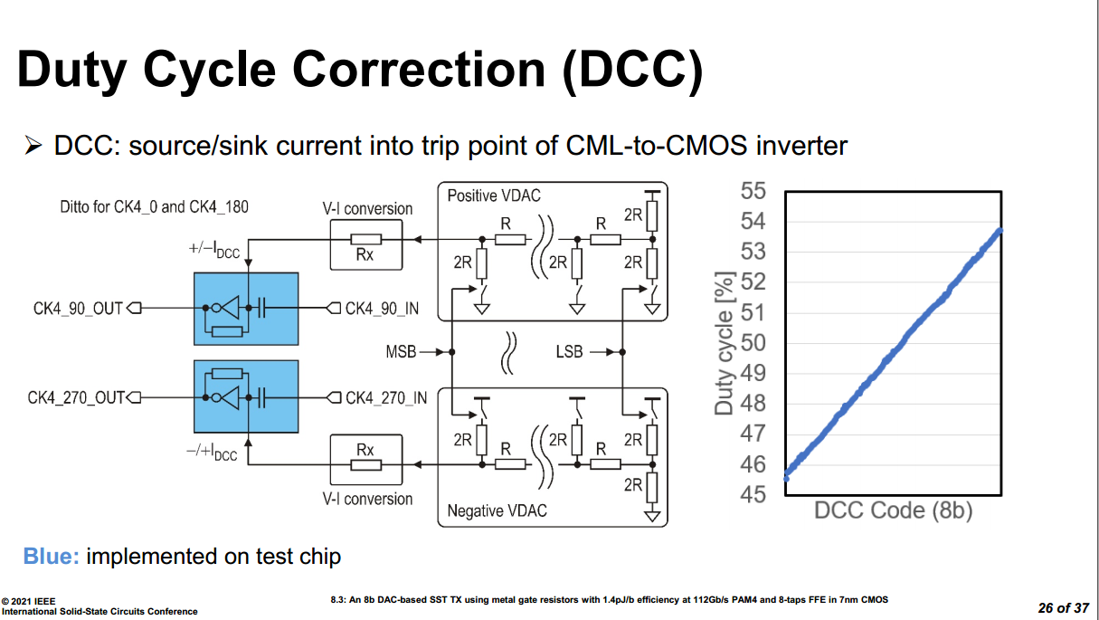
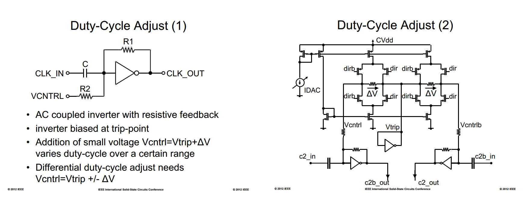
C. Menolfi et al., "A 112Gb/S 2.6pJ/b 8-Tap FFE PAM-4 SST TX in 14nm CMOS," 2018 IEEE International Solid-State Circuits Conference - (ISSCC) [https://sci-hub.se/https://doi.org/10.1109/ISSCC.2018.8310205],[visual]
M. A. Kossel et al., "8.3 An 8b DAC-Based SST TX Using Metal Gate Resistors with 1.4pJ/b Efficiency at 112Gb/s PAM-4 and 8-Tap FFE in 7nm CMOS," 2021 IEEE International Solid-State Circuits Conference (ISSCC), San Francisco, CA, USA, 2021[https://sci-hub.se/10.1109/ISSCC42613.2021.9365784]
C. Menolfi et al., "A 28Gb/s source-series terminated TX in 32nm CMOS SOI," 2012 IEEE International Solid-State Circuits Conference, San Francisco, CA, USA, 2012
Bob Lefferts, Navraj Nandra. SNUG Israel 2007 [https://picture.iczhiku.com/resource/eetop/whKYwQorwYoPUVbm.pdf]
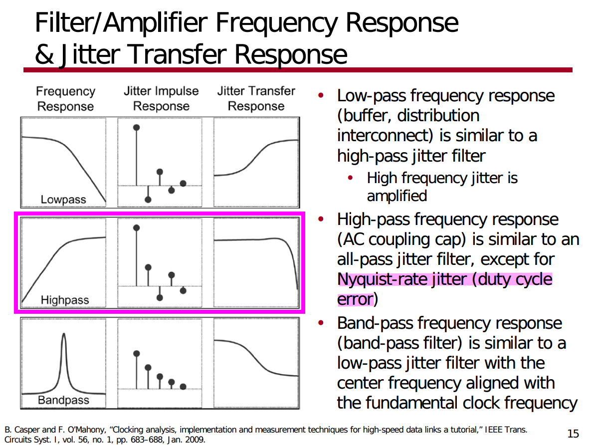
Since duty-cycle error is high frequency component, the high-pass filter suppresses the duty-cycle error propagating to the output
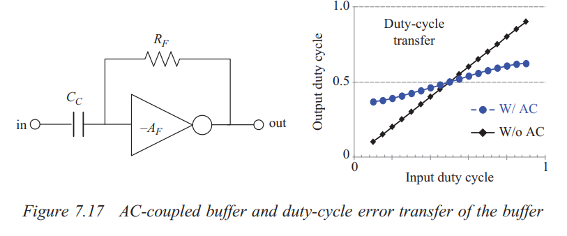
- The AC-coupling capacitor blocks the low-frequency component of the input
- The feedback resistor sets common mode voltage to the crossover voltage
Bae, Woorham; Jeong, Deog-Kyoon: 'Analysis and Design of CMOS Clocking Circuits for Low Phase Noise' (Materials, Circuits and Devices, 2020)
Casper B, O'Mahony F. Clocking analysis, implementation and measurement techniques for high-speed data links: A tutorial. IEEE Transactions on Circuits and Systems I: Regular Papers. 2009;56(1):17-39
Pulse Width Jitter (PWJ)
Pnoise sampled: Edge Delay mode measures the noise defined by two edges. Both edges are defined by a threshold voltage and rising or falling edges, which measures the noise of the pulse itself and direct plot calculate the variation of the pulse width
TODO 📅
reference
Nicola Da Dalt, Intel. ISSCC 2017 Forum: High-Performance Clock Generation and Distribution in Very-High-Speed Wireline Transceivers
Jri Lee, NTU. ISSCC 2017 Forum: Fully-Integrated Millimeter-Wave Clock Generation — From DC to 300GHz
Jihwan Kim,Intel, ISSCC 2023 Forum F1.5: Circuit Designs for 200+Gb/s Electrical Transceivers
Heng Zhang, Broadcom, ISSCC 2025 - Forum F4.2: High-speed ADCs for 100Gbps+ Wireline Transceivers
H. Zhang, D. Cui, J. Cao, and A.Momtaz, "Phase Adjustment Scheme for Time-interleaved ADCs", United States Patent. US 9065464 B2. Issued Jun.23, 2015. [https://patentimages.storage.googleapis.com/c1/11/1f/6fb830d08b710b/US9065464.pdf]
H. Zhang, D. Cui, and J. Cao, "Clock Generator for Use in A Time-interleaved ADC and Methods for Use therewith", United States Patent. US 8902094 B1. Issued Dec.2, 2014. [https://patentimages.storage.googleapis.com/c7/0b/73/74e61515ddffa2/US8902094.pdf]
rfinsights, Quadrature Phase Detector: passive mixer vs XOR gate [https://www.rfinsights.com/concepts/quadrature-phase-detector-passive-mixer-vs-xor/]
—, multiphase clock generation technique: a brief look into the history and the latest [https://www.rfinsights.com/synthesizer/multiphase-clock-generation-techniques/]
—, phase rotator in serdes - every major topology, explained [https://www.rfinsights.com/synthesizer/phase-rotator/]