High-Speed ADC for SerDes
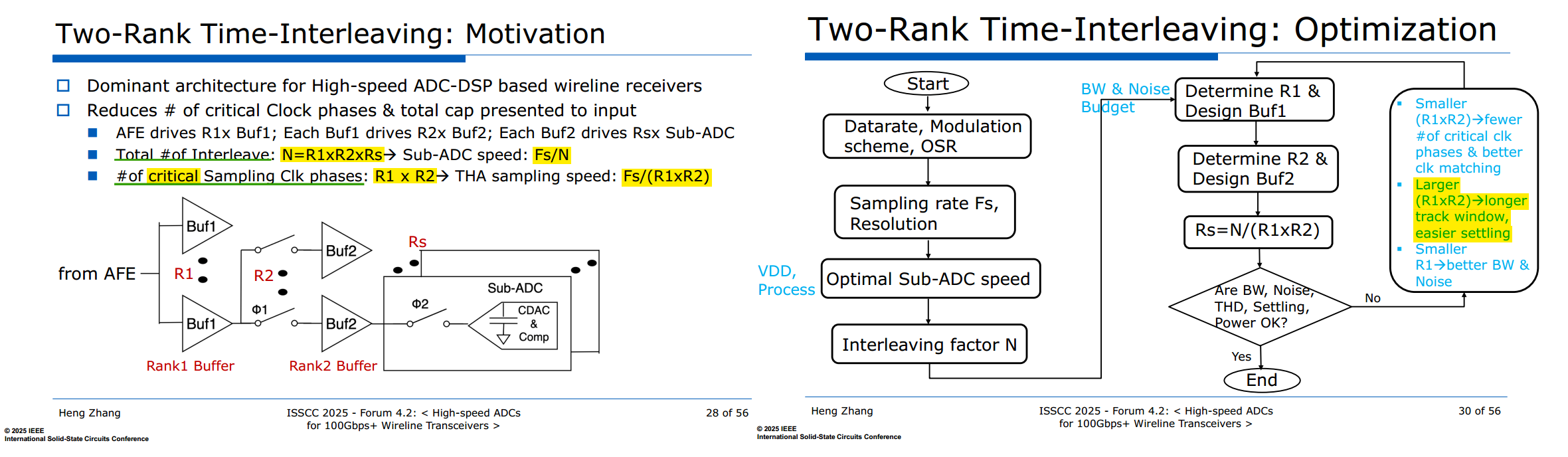
Two-Rank Time-Interleaving
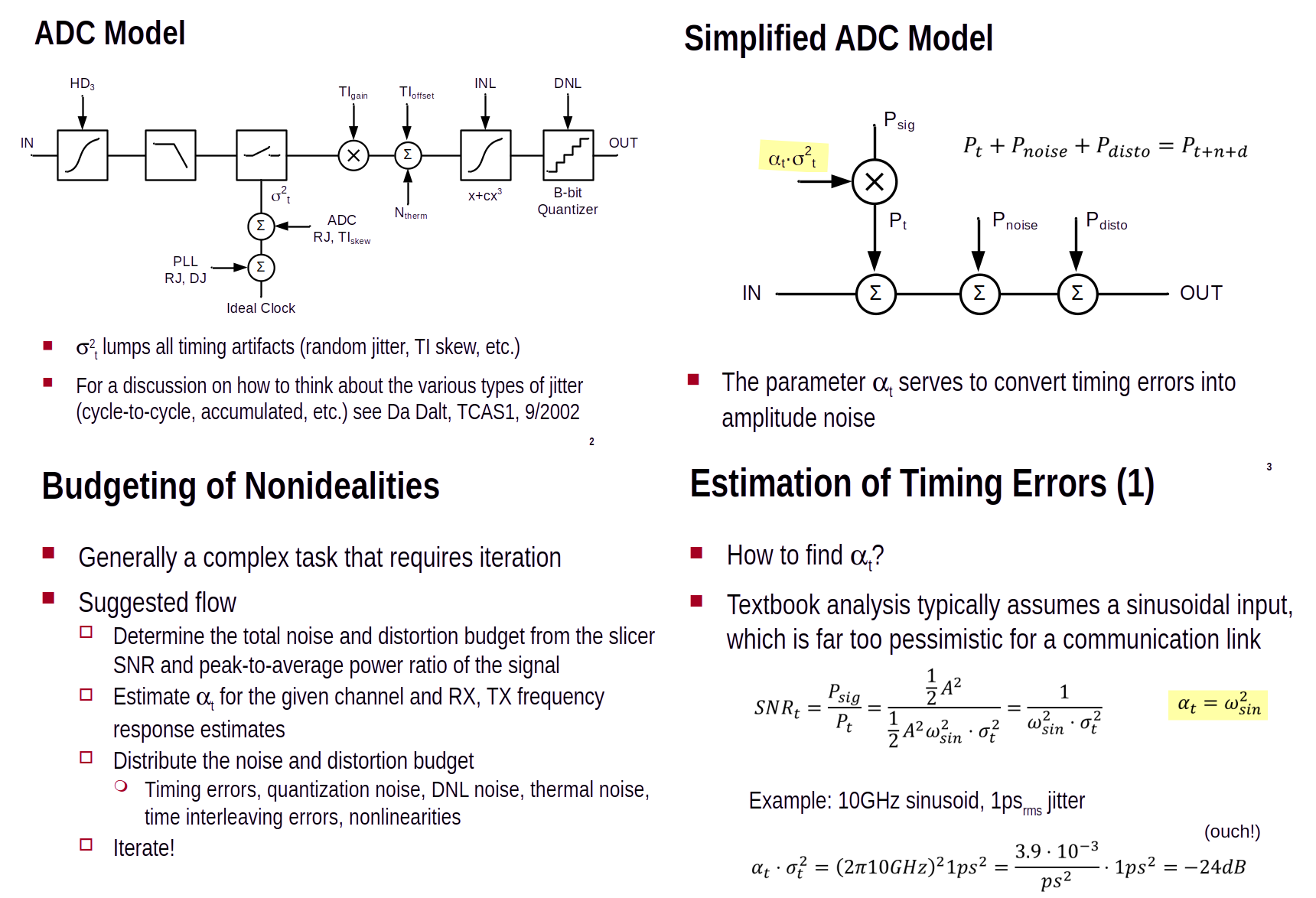
Timing Skew for Broadband signals
N. Da Dalt, M. Harteneck, C. Sandner and A. Wiesbauer, "On the jitter requirements of the sampling clock for analog-to-digital converters," in IEEE Transactions on Circuits and Systems I: Fundamental Theory and Applications, vol. 49, no. 9, pp. 1354-1360, Sept. 2002 [https://sci-hub.ru/10.1109/TCSI.2002.802353]
M. El-Chammas and B. Murmann, "General Analysis on the Impact of Phase-Skew Mismatch in Time-Interleaved ADCs," IEEE Trans. on Circuits and Systems I, vol. 56, No. 5, pp. 902-910, May 2009 [https://sci-hub.ru/10.1109/TCSI.2009.2015206]
—, "Background Calibration of Timing Skew in Time-Interleaved A/D Converters," Ph.D. Thesis, Stanford University, August 2010 [https://purl.stanford.edu/xc093xt9301]
—, "Time-Interleaved ADCs: Theory and Design," Tutorial in IEEE International Conf. on Elec., Circ., and Sys., Lebanon, December 2011 [https://el-chammas.com/papers/Manar_ICECS_handouts.pdf]
—, "The World of Time-Interleaved ADCs: From Theory to Design," Tutorial in IEEE International NEWCAS Conf., Montreal, Canada, June 2012 [https://el-chammas.com/papers/Manar_NEWCAS_TIADC_tutorial.pdf]
Dalt, Nicola Da and Ali Sheikholeslami. “Understanding Jitter and Phase Noise: A Circuits and Systems Perspective.” (2018).
Da Dalt's Approach
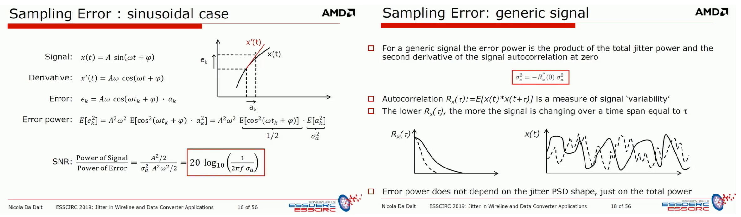
Nicola Da Dalt, ESSCIRC 2019 — Jitter in Wireline and Data Converter Applications
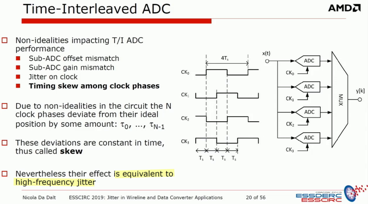
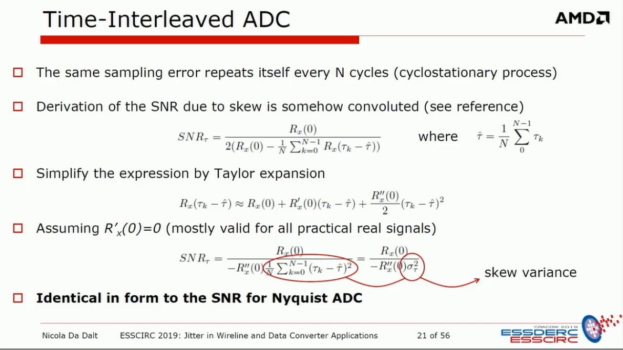
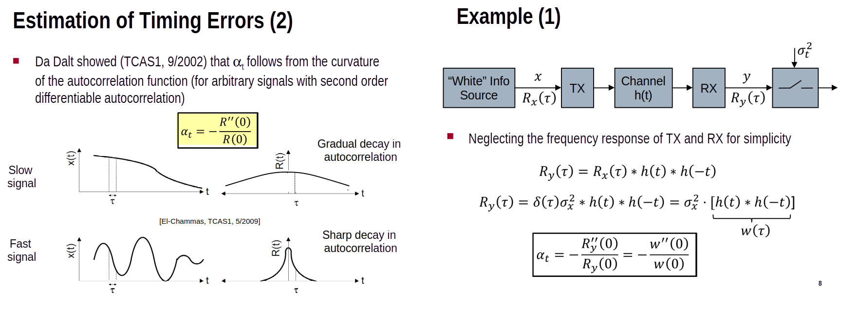
El-Chammas's Approach
El-Chammas's exact SNR is always \(\ge\) Da Dalt's: more rigorous, not more conservative
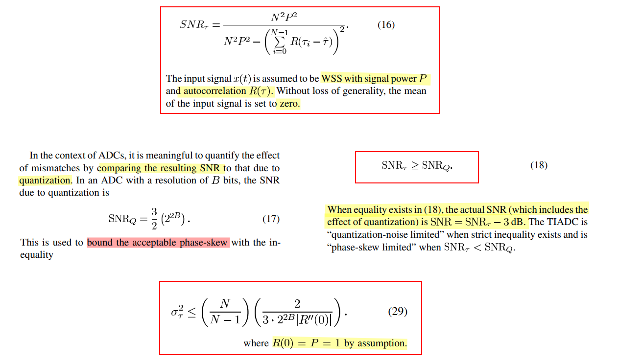
Eq. (29) above uses a normalized autocorrelation (or equivalently assumes unit signal power) — \(\color{red}R(\tau) = \frac{R_x(\tau)}{R_x(0)}\)
sinusoidal input
for a sinusoid \(x(t)=\sqrt{2}\cos(\omega t+\varphi)\), with random phase \(\varphi\sim U[0,2\pi)\) so that \(x(t)\) is WSS as (16) assumes \[ \boxed{R(\tau)=\cos\omega\tau \qquad\Rightarrow\qquad |R''(0)|=(2\pi f)^2} \]
bandlimited white noise input
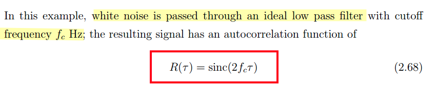
For this ideal low-pass-filtered white-noise input,
\[ \boxed{ \frac{1}{|R''(0)|} = \frac{3}{4\pi^2f_c^2}} \]
Notice the difference from the sinusoidal case:
for a sinusoid, \[ |R''(0)|=(2\pi f)^2 \]
whereas for ideal LPF white noise,
\[ \boxed{ |R''(0)|=\textcolor{red}{\frac{1}{3}}(2\pi f_c)^2} \]
That factor of \(1/3\) comes from averaging all frequencies uniformly from \(-f_c\) to \(f_c\), rather than having all the signal power concentrated at a single frequency
sinusoidal input w/ N=2
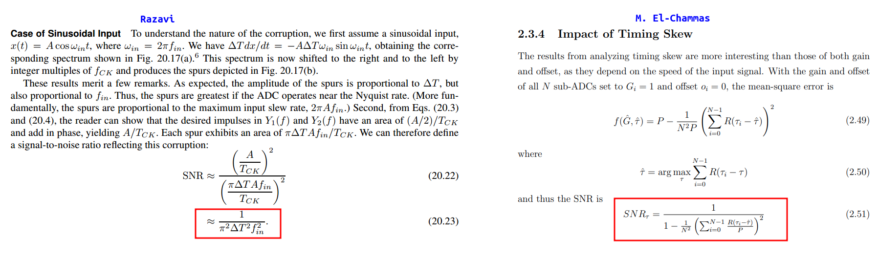
\(\hat G\) in (2.49) is the optimal common gain, \(\hat G=\frac{1}{NP}\sum_i R(\tau_i-\hat\tau)\) — see the comparison at the top of this subsection
Reducing (2.51) to (20.23)
For \(x(t)=A\cos\omega_{in}t\), the autocorrelation and power are \[ R(\tau)=\frac{A^2}{2}\cos\omega_{in}\tau\qquad P=R(0)=\frac{A^2}{2}\qquad\Rightarrow\qquad\frac{R(\tau)}{P}=\cos\omega_{in}\tau \]
In Razavi's model, one channel samples on time and the other samples \(\Delta T\) late, so \(\tau_0=0\) and \(\tau_1=\Delta T\). The sum in (2.50) becomes
\[ \cos\omega_{in}\tau+\cos\omega_{in}(\Delta T-\tau)=2\cos\left(\frac{\omega_{in}\Delta T}{2}\right)\cos\left[\omega_{in}\left(\tau-\frac{\Delta T}{2}\right)\right] \]
This is largest at \(\hat{\tau}=\Delta T/2\), where it equals \(2\cos(\pi f_{in}\Delta T)\). Substituting into (2.51), the \(1/N^2=1/4\) cancels the \(2^2\):
\[ SNR_\tau=\frac{1}{1-\cos^2(\pi f_{in}\Delta T)}=\frac{1}{\sin^2(\pi f_{in}\Delta T)}\approx\frac{1}{\pi^2\Delta T^2 f_{in}^2} \]
The last step uses \(\sin x\approx x\), and the result is exactly (20.23).
Murmann's Lecture
Boris Murmann, August 2013 Lectures on Circuit and Architecture Design for High-Speed ADCs — Determining ADC specs from system specs [https://bbs.eetop.cn/thread-979682-1-1.html]
Timing Skew Calibration
M. El-Chammas and B. Murmann, "A 12-GS/s 81-mW 5-bit Time-Interleaved Flash ADC With Background Timing Skew Calibration," in IEEE Journal of Solid-State Circuits, vol. 46, no. 4, pp. 838-847, April 2011 [https://sci-hub.ru/10.1109/JSSC.2011.2108125]
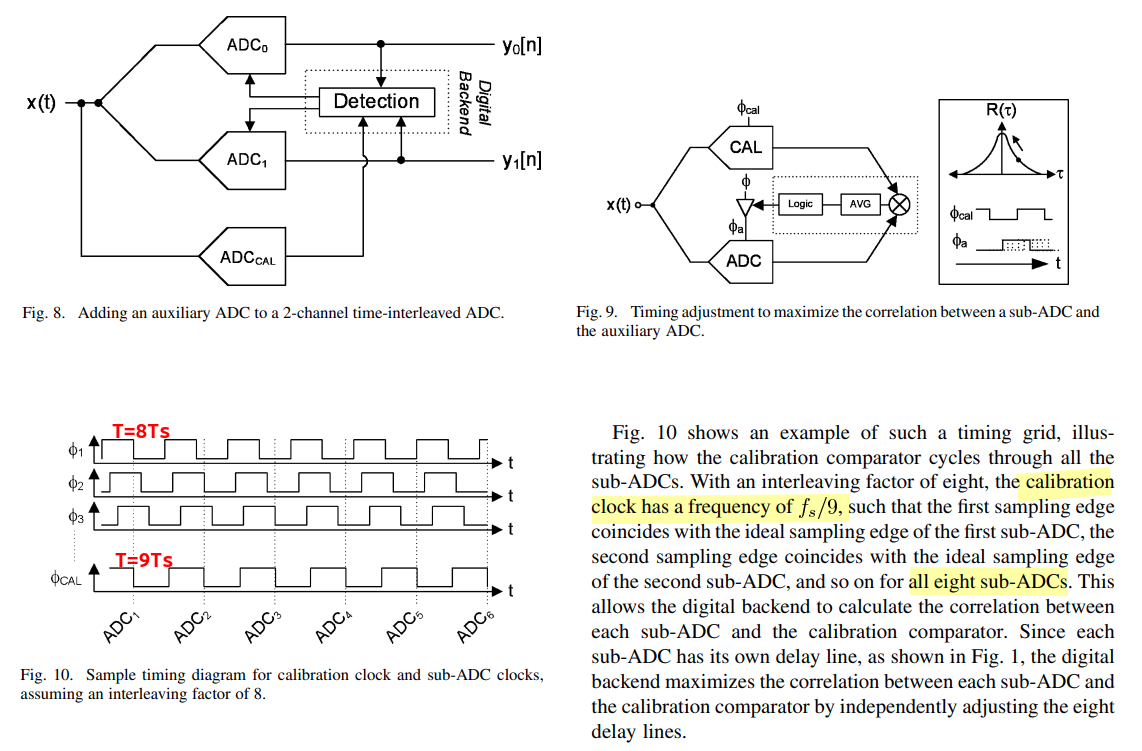
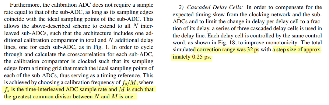
The total simulated correction range was 32 ps with a step size of approximately 0.25 ps
Ts = 1/12G=84 ps. correction range is about half Ts
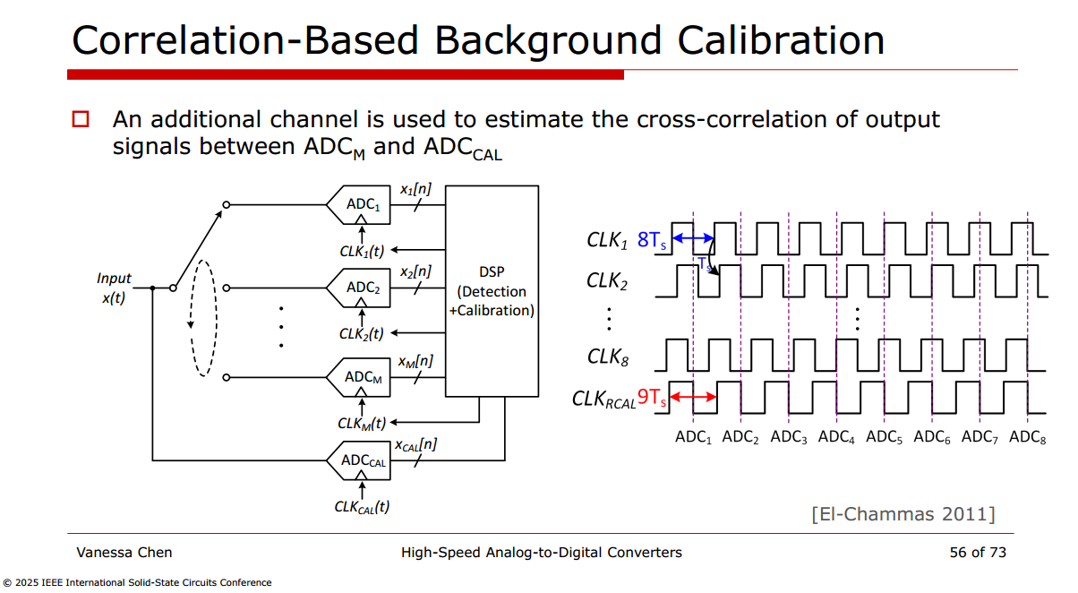
| 0 | 1 | 2 | 3 | 4 | 5 | 6 | 7 | 8 | |
|---|---|---|---|---|---|---|---|---|---|
| \(\phi_1\) | 0 | 8 | 16 | 24 | 32 | 40 | 48 | 56 | 64 |
| \(\phi_{CAL}\) | 0 | 9 | 18 | 27 | 36 | 45 | 54 | 63 | 72 |
| \((\phi_{CAL}-\phi_1)\%8\) | 0 | 1 | 2 | 3 | 4 | 5 | 6 | 7 | 0 |
Let the calibration clock be
\[ t_{\mathrm{CAL}}[m]=\delta+9mT_s \]
where \(\delta\) is an arbitrary initial phase.
For ADC \(i\), its ideal sampling instants are
\[ t_i[k]=iT_s+8kT_s \]
The time difference is
\[ \Delta t = \delta+9mT_s-iT_s-8kT_s \]
Because \(\gcd(9,8)=1\), the quantity
\[ 9m-i-8k \]
can actually take any integer value \(q\). Therefore,
\[ \Delta t=\delta+qT_s \]
We can choose the pair of CAL/ADC edges that makes
\[ |\delta+qT_s| \]
minimum. Thus the physically relevant residual offset can be written as \[ \boxed{ \Delta t_{\min} = \delta\pmod{T_s} } \]
with the centered choice satisfying
\[ \boxed{ |\Delta t_{\min}|\le \frac{T_s}{2} } \]
The 32-ps DCDL is not enough to tolerate a completely arbitrary phase offset between \(CLK_{\mathrm{RCAL}}\) and the ideal ADC sampling grid.
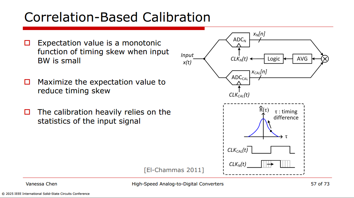
The CAL clock must therefore be coarsely phase-positioned sufficiently close to the ADC sampling grid, while the 32-ps delay lines handle residual skew/fine alignment. The paper explicitly requires the CAL sampling edges to form a timing grid matching the ideal sub-ADC sampling points.
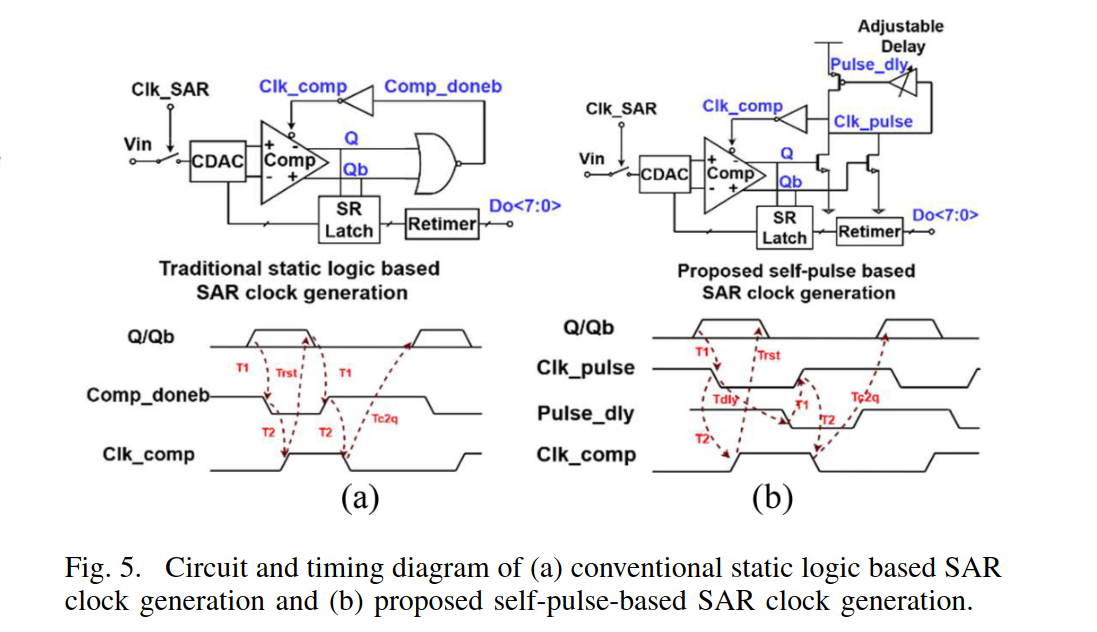
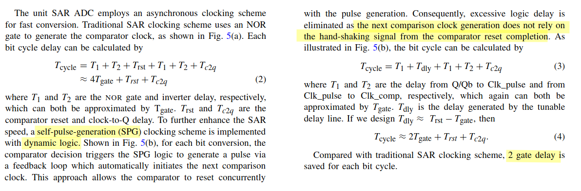
self-pulse-generation (SPG)
C. Liu et al., "An 800GbE PAM-4 PHY Transceiver that Supports 42dB Copper and Direct-Drive Optical Applications in 7nm," 2025 IEEE Custom Integrated Circuits Conference (CICC), Boston, MA, USA, 2025, pp. 1-3, doi: 10.1109/CICC63670.2025.10983780.
—, "An 800GbE PAM-4 PHY Transceiver for 42 dB Copper and Direct-Drive Optical Applications in 7 nm," in IEEE Solid-State Circuits Letters, vol. 8, pp. 281-284, 2025, doi: 10.1109/LSSC.2025.3608134
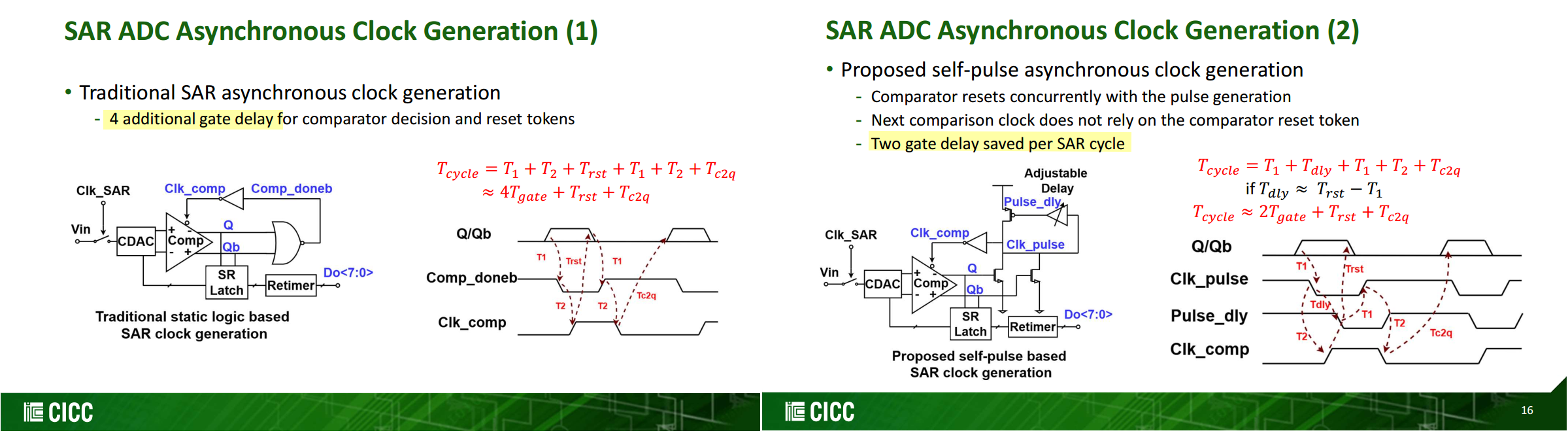
Taking the initial Q/Qb rising edge as \(t=0\):
\[ t_{\mathrm{Clk\_pulse}\uparrow} =T_1+T_{\mathrm{dly}}+T_1 =T_1+T_{\mathrm{rst}} \]
whereas
\[ t_{\mathrm{Q/Qb}\downarrow} =T_1+T_2+T_{\mathrm{rst}} \]
Therefore, the model predicts Clk_pulse rising
\(T_2\) before Q/Qb finish
resetting. This also conflicts with the drawing, which places
Q/Qb falling before Clk_pulse rises.
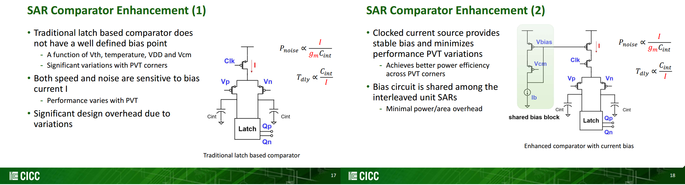
The qualification is that this compares their instantaneous
currents during reset: Q/Qb may already be falling
and weakening the NMOS. It does not necessarily require the PMOS to
overpower a fully enabled NMOS under all conditions.
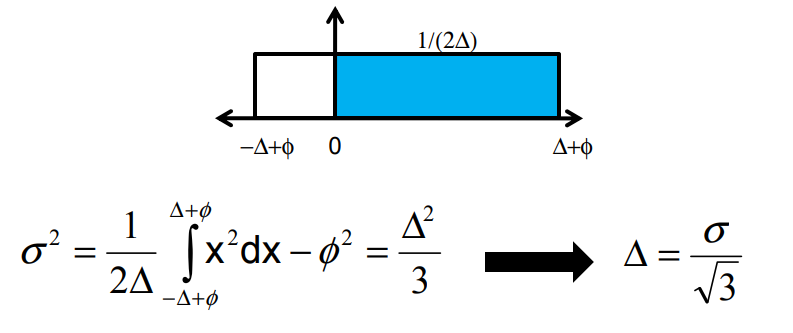
BER with Quantization Noise
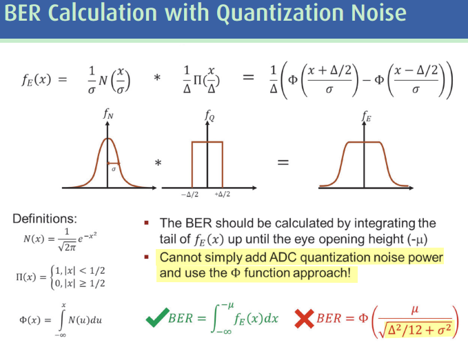
\[ \text{Var}(X) = E[X^2] - E[X]^2 \]
ADC sampling front-end (SFE)
K. Sun, G. Wang, Q. Zhang, S. Elahmadi and P. Gui, "A 56-GS/s 8-bit Time-Interleaved ADC With ENOB and BW Enhancement Techniques in 28-nm CMOS," in IEEE Journal of Solid-State Circuits, vol. 54, no. 3, pp. 821-833, March 2019 [https://sci-hub.ru/10.1109/JSSC.2018.2884352]
Y. Shifman, Y. Krupnik, U. Virobnik, A. Khairi, Y. Sanhedrai and A. Cohen, "A 1.64mW Differential Super Source-Follower Buffer with 9.7GHz BW and 43dB PSRR for Time-Interleaved ADC Applications in 10nm," 2019 IEEE Asian Solid-State Circuits Conference (A-SSCC), Macau, Macao, 2019 [https://sci-hub.ru/10.1109/A-SSCC47793.2019.9056969]
Y. Krupnik et al., "112-Gb/s PAM4 ADC-Based SERDES Receiver With Resonant AFE for Long-Reach Channels," in IEEE Journal of Solid-State Circuits, vol. 55, no. 4, pp. 1077-1085, April 2020 [https://sci-hub.ru/10.1109/JSSC.2019.2959511]
G. Li et al., "18.1 A 600Gb/s DP-QAM64 Coherent Optical Transceiver Frontend with 4x10⁵GS/s 8b ADC/DAC in 16nm CMOS," 2024 IEEE International Solid-State Circuits Conference (ISSCC), San Francisco, CA, USA, 2024, pp. 338-340 [https://sci-net.xyz/10.1109/ISSCC49657.2024.10454499]
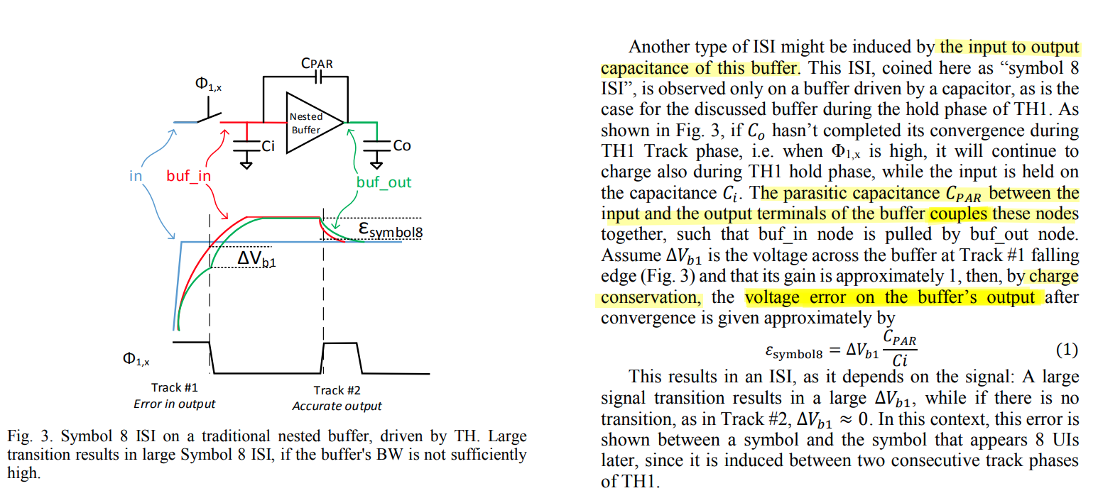
By charge conservation at the input of this buffer
\[ V_iC_i + \Delta V_{b1}C_{PAR} = V_{bo}C_i \qquad \Longrightarrow \qquad V_{bo} = V_i + \color{blue}\Delta V_{b1}\frac{C_{PAR}}{C_i} \]
i.e.
\[ \varepsilon_\text{symbol8} = \Delta V_{b1}\frac{C_{PAR}}{C_i} \]
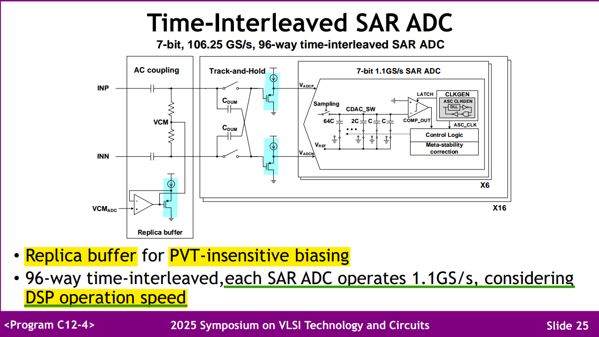
PVT-insensitive biasing
K. Kwon et al., "C12-4 A 212.5Gb/s Pam-4 Receiver With Mutual Inductive Coupled Gm-Tia in 4nm Finfet," 2025 Symposium on VLSI Technology and Circuits (VLSI Technology and Circuits), Kyoto, Japan, 2025, pp. 1-3, doi: 10.23919/VLSITechnologyandCir65189.2025.11074881.
Replica buffer for PVT-insensitive biasing
SFE Pulse Response
Y. Frans, "ADC-based Wireline Transceiver," 2019 IEEE Custom Integrated Circuits Conference (CICC), Austin, TX, USA, 2019, pp. 1-89 [https://sci-hub.jp/10.1109/CICC.2019.8780306]
J. Im et al., "6.1 A 112Gb/s PAM-4 Long-Reach Wireline Transceiver Using a 36-Way Time-Interleaved SAR-ADC and Inverter-Based RX Analog Front-End in 7nm FinFET," 2020 IEEE International Solid-State Circuits Conference - (ISSCC), San Francisco, CA, USA, 2020, pp. 116-118 [https://sci-hub.ru/10.1109/ISSCC19947.2020.9063081]
—, "A 112-Gb/s PAM-4 Long-Reach Wireline Transceiver Using a 36-Way Time-Interleaved SAR ADC and Inverter-Based RX Analog Front-End in 7-nm FinFET," in IEEE Journal of Solid-State Circuits, vol. 56, no. 1, pp. 7-18, Jan. 2021 [https://sci-hub.ru/10.1109/JSSC.2020.3024261]
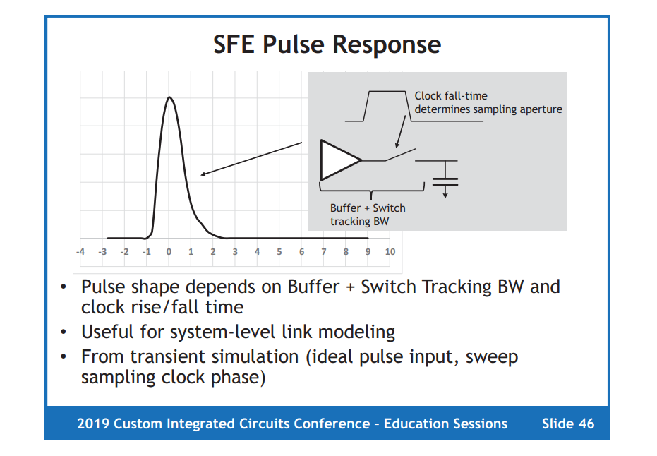
sweep the setup time between ideal pulse input and clock, sample the output of SFE at falling edge
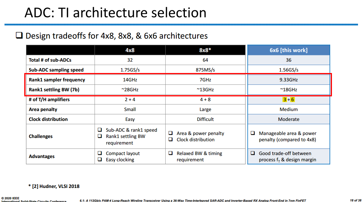
The front-end (Rank-1) tracking bandwidth scales linearly to approximately twice the sampling frequency
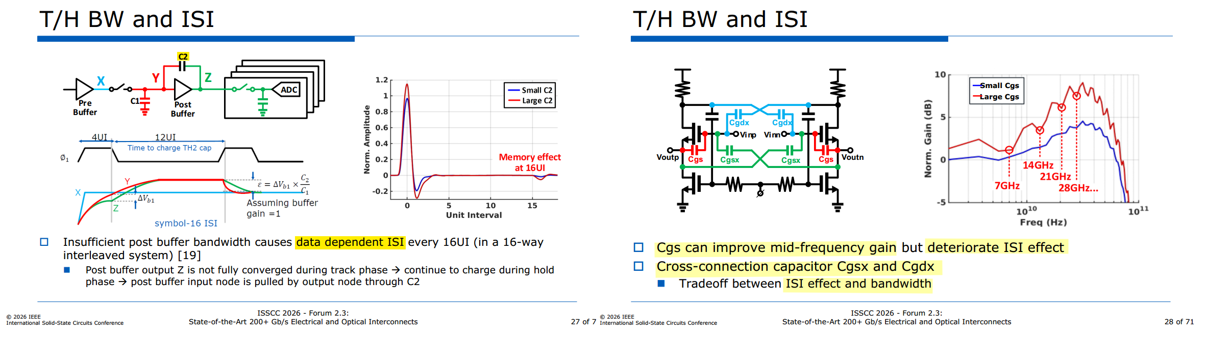
T/H BW & ISI
N. G. Jayaraman, “High speed buffering for time-interleaved ADCs with reduced ISI and increased voltage gain,” WO Patent 2018164928 A1, Sep. 13, 2018. [Online]. Available: [https://patents.google.com/patent/WO2018164928A1]
T. Ali et al., "6.4 A 180mW 56Gb/s DSP-Based Transceiver for High Density IOs in Data Center Switches in 7nm FinFET Technology," 2019 IEEE International Solid-State Circuits Conference - (ISSCC), San Francisco, CA, USA, 2019, pp. 118-120 [https://sci-hub.se/10.1109/ISSCC.2019.8662523]
E. -H. Chen et al., "7.1 A 212.5Gb/s DSP-Based PAM-4 Transceiver with 50dB Loss Compensation for Large AI System Interconnects in 4nm FinFET," 2025 IEEE International Solid-State Circuits Conference (ISSCC), San Francisco, CA, USA, 2025, pp. 1-3, doi: 10.1109/ISSCC49661.2025.10904601.
TODO 📅
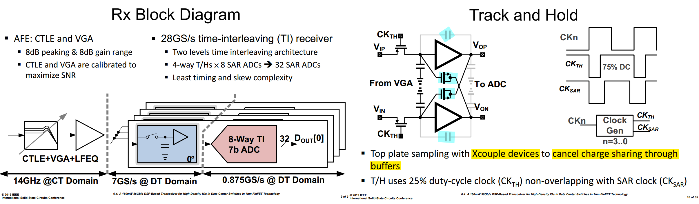
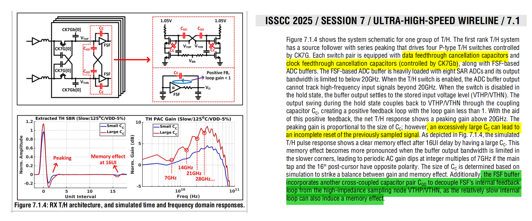
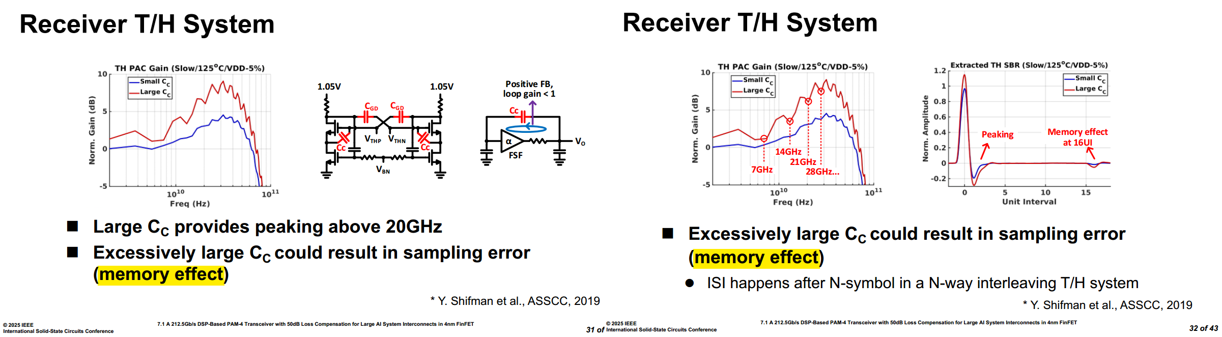
G. Li et al., "18.1 A 600Gb/s DP-QAM64 Coherent Optical Transceiver Frontend with 4x10⁵GS/s 8b ADC/DAC in 16nm CMOS," 2024 IEEE International Solid-State Circuits Conference (ISSCC), San Francisco, CA, USA, 2024, pp. 338-340 [https://sci-net.xyz/10.1109/ISSCC49657.2024.10454499]
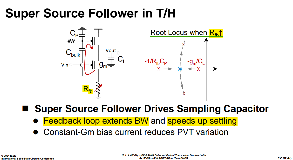
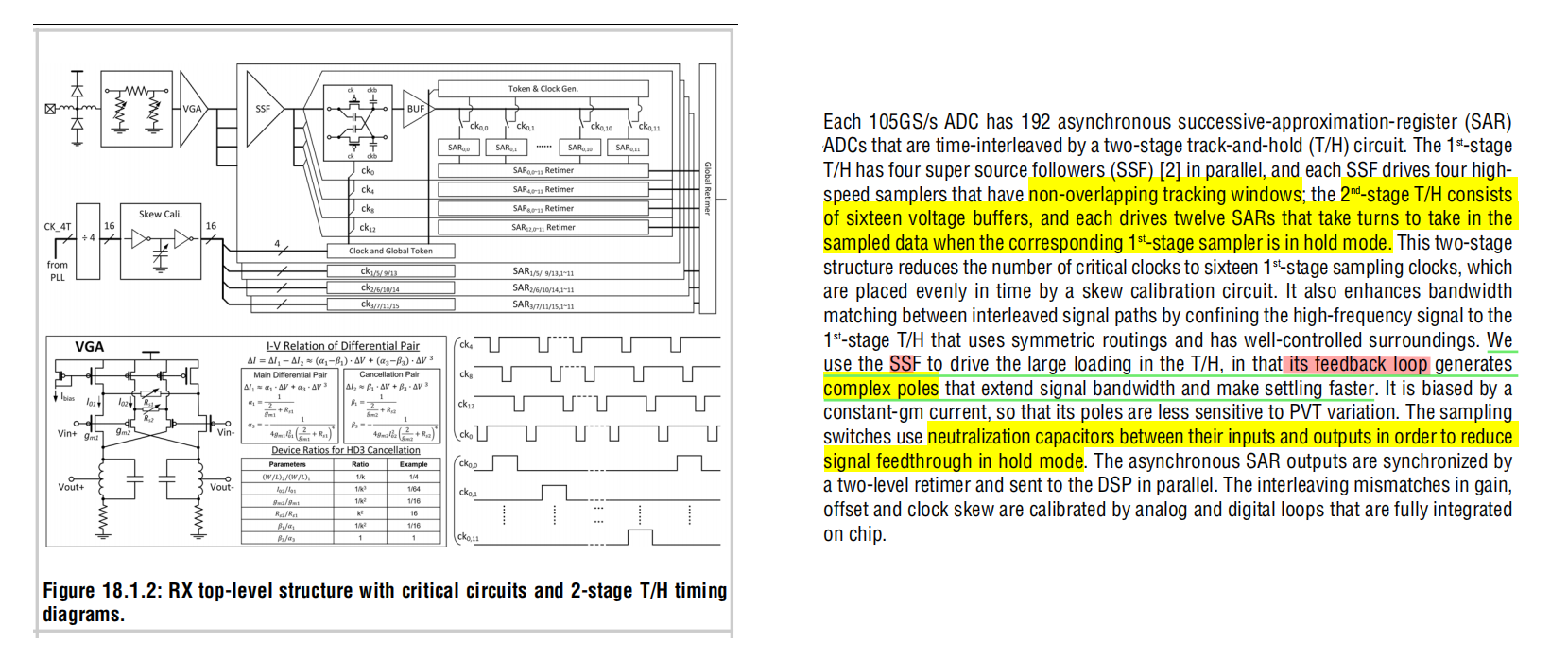
SSF transfer function & complex poles
PMOS input device \(g_m\) (gate \(V_i\), source \(V_o\), drain \(V_p\)), PMOS feedback device \(g_{mp}\) (gate \(V_p\), drain \(V_o\)). \(C_{bulk}\) is treated as AC short and \(g_{ds}\) is omitted
KCL at \(V_o\) and \(V_p\) \[\begin{align} g_m(V_i-V_o) &= g_{mp}V_p + sC_LV_o \\ g_m(V_o-V_i) &= V_p\left(\frac{1}{R_{fb}}+sC_p\right) \end{align}\]
i.e. \(V_p=\frac{g_mR_{fb}(V_o-V_i)}{1+sR_{fb}C_p}\), substitute into the first one \[ V_i\left[g_m+\frac{g_mg_{mp}R_{fb}}{1+sR_{fb}C_p}\right] = V_o\left[g_m+\textcolor{red}{\frac{g_mg_{mp}R_{fb}}{1+sR_{fb}C_p}}+sC_L\right] \]
The red term is the loop through \(V_o\). Dropping it leaves only the open-loop poles \(-g_m/C_L\) and \(-1/R_{fb}C_p\), and gives DC gain \(1+g_{mp}R_{fb}\neq 1\)
\[ \boxed{H(s)=\frac{V_o}{V_i}=\frac{g_m(1+g_{mp}R_{fb}+sR_{fb}C_p)}{s^2R_{fb}C_pC_L+s(C_L+g_mR_{fb}C_p)+g_m(1+g_{mp}R_{fb})}} \]
\(H(0)=1\), and LHP zero at \(-(1+g_{mp}R_{fb})/R_{fb}C_p\approx -g_{mp}/C_p\)
Break the loop at gate of \(g_{mp}\), the loop gain is \[ T(s)=\frac{g_{mp}R_{fb}}{(1+s\tau_L)(1+s\tau_p)}\qquad \tau_L=\frac{C_L}{g_m},\quad \tau_p=R_{fb}C_p \]
The denominator of \(H(s)\) is \(\propto 1+T(s)\), i.e. two-pole negative feedback: two open-loop poles move toward each other, meet and then split into complex pair as \(g_{mp}R_{fb}\) increases \[\begin{align} \omega_n^2 &= \frac{1+g_{mp}R_{fb}}{\tau_L\tau_p} \approx \frac{g_mg_{mp}}{C_LC_p} \\ Q &= \frac{\sqrt{(1+g_{mp}R_{fb})\,\tau_L\tau_p}}{\tau_L+\tau_p} \end{align}\]
complex poles (\(Q>1/2\)) when \[ g_{mp}R_{fb} > \frac{1}{4}\left(\sqrt{\frac{\tau_p}{\tau_L}}-\sqrt{\frac{\tau_L}{\tau_p}}\right)^2 \]
reference
Samuel Palermo, ISSCC 2018 T10: ADC-Based Serial Links: Design and Analysis
Yohan Frans, CICC2019 ES3-3- "ADC-based Wireline Transceivers" [https://sci-hub.jp/10.1109/CICC.2019.8780306]
Nhat Nguyen and Masum Hossain, ISSCC 2021 Forum F6.7: 112Gb/s-and-Beyond Long-Reach and Short-Reach Electrical Interfaces
Jihwan Kim, Intel, ISSCC 2023 Forum F1.5: Circuit Designs for 200+Gb/s Electrical Transceivers
Ben Rhew, Samsung, ISSCC 2023 F5.6 Extreme Data Converters and Their Peripherals: High Performance ADC Design in High-Speed Wireline Transceivers and 5G Wireless Transceiver
Ariel Cohen, Intel, ISSCC 2024 Forum F6.3: Beyond 200Gbps Electrical transceivers – Circuit Architecture, Design Implementation and Silicon Results
Heng Zhang, Broadcom, ISSCC 2025 Forum F4.2: High-speed ADCs for 100Gbps+ Wireline Transceivers
V. Chen, "Tutorial: High-Speed Analog-to-Digital Converters," 2025 IEEE International Solid-State Circuits Conference (ISSCC), San Francisco, CA, USA, 2025, pp. 1-1, doi: 10.1109/ISSCC49661.2025.11076112.
E-Hung Chen, MTK, ISSCC 2026 Forum F2.3: State-of-the-Art 200+ Gb/s Electrical and Optical Interconnects
T. Chan Carusone, T. O. Dickson, S. Palermo, S. Shekhar and M. Mansuri, "Modern Wireline Transceivers," in IEEE Journal of Solid-State Circuits, vol. 61, no. 2, pp. 395-422, Feb. 2026 [https://ieeexplore.ieee.org/stamp/stamp.jsp?arnumber=11311714]
Akkaya, A. (2021). High-Speed ADC Design and Optimization for Wireline Links (Publication No. 8453) [PhD thesis, EPFL; Supervised by Y. Leblebici]. [https://doi.org/10.5075/epfl-thesis-8453]
K. Zheng, “System-driven circuit design for ADC-based wireline data links,” Stanford Univ., Stanford, CA, USA, Tech. Rep., 2018 [https://stacks.stanford.edu/file/hw458fp0168/thesis-augmented.pdf]
Kull, Lukas, Thomas Toifl, Martin L. Schmatz, Pier Andrea Francese, Christian Menolfi, Matthias Braendli, Marcel A. Kossel, Thomas Morf, Toke Meyer Andersen and Yusuf Leblebici. “22.1 A 90GS/s 8b 667mW 64× interleaved SAR ADC in 32nm digital SOI CMOS.” 2014 IEEE International Solid-State Circuits Conference Digest of Technical Papers (ISSCC) (2014): 378-379. [https://sci-hub.jp/10.1109/ISSCC.2014.6757477]
—. (2014). High-Speed CMOS ADC Design for 100Gb/s Communication Systems (Publication No. 6037) [PhD thesis, EPFL; Supervised by Y. Leblebici]. https://doi.org/10.5075/epfl-thesis-6037
—., "A 3.1mW 8b 1.2GS/s single-channel asynchronous SAR ADC with alternate comparators for enhanced speed in 32nm digital SOI CMOS," 2013 IEEE International Solid-State Circuits Conference Digest of Technical Papers, San Francisco, CA, USA, 2013, pp. 468-469 [https://sci-hub.jp/10.1109/ISSCC.2013.6487818]
—., "A 3.1 mW 8b 1.2 GS/s Single-Channel Asynchronous SAR ADC With Alternate Comparators for Enhanced Speed in 32 nm Digital SOI CMOS," in IEEE Journal of Solid-State Circuits, vol. 48, no. 12, pp. 3049-3058, Dec. 2013 [https://sci-hub.jp/10.1109/JSSC.2013.2279571]
G. Manganaro, "An Introduction to High Sample Rate Nyquist Analog-to-Digital Converters," in IEEE Open Journal of the Solid-State Circuits Society, vol. 2, pp. 82-102, 2022 [https://ieeexplore.ieee.org/stamp/stamp.jsp?arnumber=9911689]