Multiphase Clock Generation
QEC (Quadrature Error Corrector )
Shaokang ZHAO, 2025, "Multi-Phase Clock Generator for High-Speed Wireline Systems," [paper, slides]
TODO 📅
AC-coupled buffer & DCC
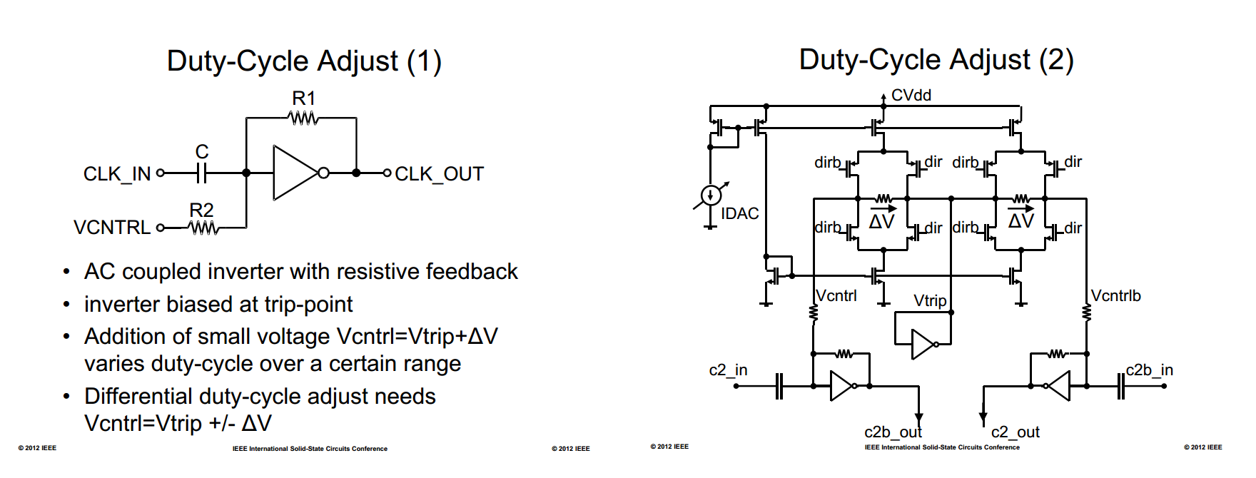
The amount of correction can be set by intentional injection of an offset current into the summing input node of INV, threshold-adjustable inverter
Note that the change to the threshold is opposite in direction to the change to INV
increasing DC of input signal is equivalent to lower down the threshold of INV
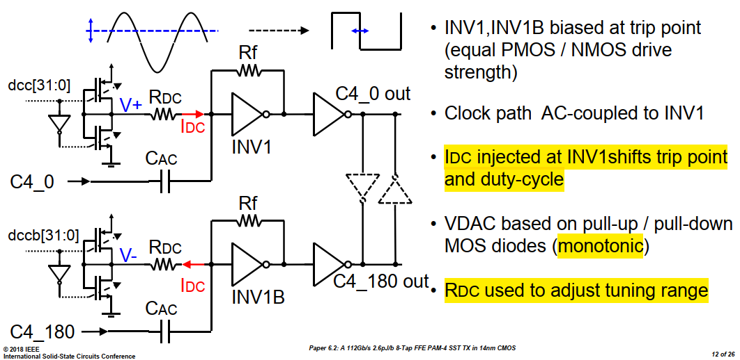
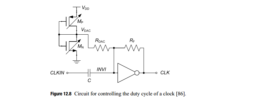
voltage at INV1 will increased by: \[ \frac{\Delta V_{DAC} - \Delta {INV1}}{R_{DAC}} = \frac{\Delta {INV1} +A_0 \Delta {INV1}}{R_{F}} \] therefore \[ \Delta {INV1} = \Delta V_{DAC} \cdot \frac{R_F}{R_F+(A_0+1)R_{DAC}} \approx \Delta V_{DAC} \cdot \frac{R_F}{A_0R_{DAC}} \]
variable \(R_{DAC}\) can be used to tweak tuning resolution & range
If \(R_{DAC} = R_F\) \[ \Delta {INV1}\approx \frac{\Delta V_{DAC}}{A_0} \]
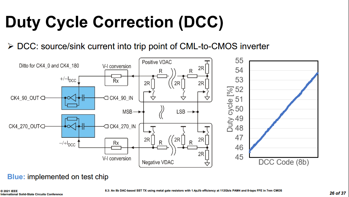
C. Menolfi et al., "A 112Gb/S 2.6pJ/b 8-Tap FFE PAM-4 SST TX in 14nm CMOS," 2018 IEEE International Solid-State Circuits Conference - (ISSCC) [https://sci-hub.se/https://doi.org/10.1109/ISSCC.2018.8310205],[visual]
M. A. Kossel et al., "8.3 An 8b DAC-Based SST TX Using Metal Gate Resistors with 1.4pJ/b Efficiency at 112Gb/s PAM-4 and 8-Tap FFE in 7nm CMOS," 2021 IEEE International Solid-State Circuits Conference (ISSCC), San Francisco, CA, USA, 2021[https://sci-hub.se/10.1109/ISSCC42613.2021.9365784]
C. Menolfi et al., "A 28Gb/s source-series terminated TX in 32nm CMOS SOI," 2012 IEEE International Solid-State Circuits Conference, San Francisco, CA, USA, 2012
Bob Lefferts, Navraj Nandra. SNUG Israel 2007 [https://picture.iczhiku.com/resource/eetop/whKYwQorwYoPUVbm.pdf]
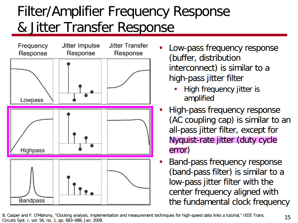
Since duty-cycle error is high frequency component, the high-pass filter suppresses the duty-cycle error propagating to the output
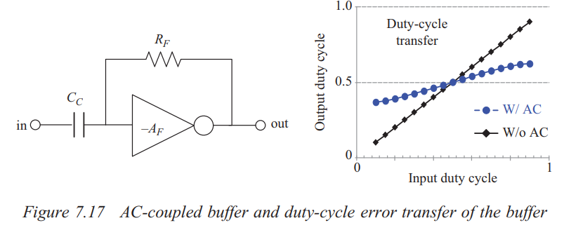
- The AC-coupling capacitor blocks the low-frequency component of the input
- The feedback resistor sets common mode voltage to the crossover voltage
Bae, Woorham; Jeong, Deog-Kyoon: 'Analysis and Design of CMOS Clocking Circuits for Low Phase Noise' (Materials, Circuits and Devices, 2020)
Casper B, O'Mahony F. Clocking analysis, implementation and measurement techniques for high-speed data links: A tutorial. IEEE Transactions on Circuits and Systems I: Regular Papers. 2009;56(1):17-39
Pulse Width Jitter (PWJ)
Pnoise sampled: Edge Delay mode measures the noise defined by two edges. Both edges are defined by a threshold voltage and rising or falling edges, which measures the noise of the pulse itself and direct plot calculate the variation of the pulse width
TODO 📅