VCS & Verdi
VCS with customized UVM version
1 | # uvm 1.1 customized |
VCS with release UVM
1 | $ vcs -full64 -debug_access+all -kdb -sverilog -ntb_opts uvm-1.2 |
VCS compile-time options
-kdb: Enables generating Verdi KDB database
-lca: Enables Limited Customer Availability feature, which is not fully test
+vpi: Enables the use of VPI PLI access routines.
Verilog PLI (Programming Language Interface) is a mechanism to invoke C or C++ functions from Verilog code.
-P <pli.tab>: Specifies a PLI table file
${VERDI_HOME}/share/PLI/VCS/LINUX64/novas.tb
+define+ifdef compiler directive
+define+SIMULATION when compiling
`ifdef SIMULATOIN in code
-debug_access: Enables dumping to FSDB/VPD, and
limited read/callback capability. Use -debug_access+classs
for testbench debug, and debug_access+all for all debug
capabilities. Refer the VCS user guide for more granular options for
debug control under the switch debug_access and refer to
debug_region for region control
-y
-v <filename>: Specifies a Verilog library file to search for module definitons
+nospecify: Suppresses module path delays and time checks in specify blocks
-l <filename>: (lower case L) Specifies a log file where VCS records compilation message and runtime messages if you include the -R, -RI, or -RIG option
+vcs+fsdbon: A compile-time
substitute for $fsdbDumpvars system task. The
+vcs+fsdbon switch enables dumping for the entire
design. If you do not add a corresponding
-debug_access* switch, then -debug_access is
automatically added. Note that you must also set
VERDI_HOME.
$ ./simv
FSDB Dumper for VCS, Release Verdi_S-2021.09-SP2-2, Linux x86_64/64bit, 05/22/2022 (C) 1996 - 2022 by Synopsys, Inc. *Verdi* : Create FSDB file 'novas.fsdb' *Verdi* : Begin traversing the scopes, layer (0). *Verdi* : End of traversing.
+vcs+vcdpluson: A compile-time
substitute for $vcdpluson system task. The
+vcs+vcdpluson switch enables dumping for the entire
design. If you do not add a corresponding
-debug_access* switch, then -debug_access is
automatically added
$ ./simv
VCD+ Writer S-2021.09-SP2-2_Full64 Copyright (c) 1991-2021 by Synopsys Inc.
+incdir+<directory>: Specifies the directories
that contain the files you specified with the `include
compiler directive. You can specify more than on directory, separating
each path name with the + character.
Compile time Use Model
Just add the -kdb option to VCS executables when running
simulation
Three steps flow:
vlogan/vhdlan/syscan -kdbCompile design and generate un-resolved KDB to ./work
vcs -kdb -debug_access+all <other option>Generate elaborated KDB to ./sim.dadir
Two steps flow:
vcs -kdb -debug_access+all <other option>Compile design and generate elaborated KDB to ./simv.dadir
Common simv Option
-gv <gen=value>: override runtime VHDL generics
*
-ucli: stop at Tcl prompt upon start-up
-i <run.tcl>: execute specified Tcl script upon
start-up
-l <logfile>: create runtime logfile
-gui: create runtime logfile
-xlrm: allow relaxed/non-LRM compliant code
-cm <options>: enable coverate options
verdi binkey
SHIFT+A: Find Signal/Find Instance/Find
Instport
SHIFT+S: Find Scope
module traverse

Show Calling
Show Definition
Double-Click instance name is same with click Show Definition
Double-Click module name is same with click Show Calling
signal traverse

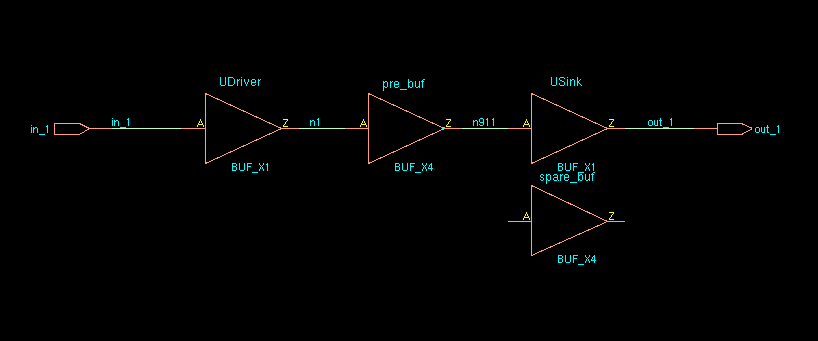
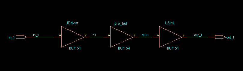
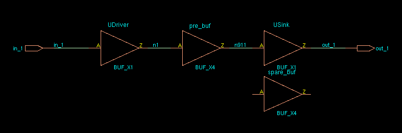
Driver
Load
Double-Click signal name is same with click Driver
Verdi options
-ssf fastFile(s)|dumpFile(s)|fastFile list(s): Load FSDB
(*.fsdb), virtual FSDB (*.vf) , gzipped FSDB (*.fsdb.gz), bzip2 FSDB
(*.fsdb.bz2), waveform dump (*.vcd, *.vcd.gz) files, or FSDB file list
(*.flst)
-simBin <simv_executable>: Specify the path of the
simulation binary file.

-dbdir: Specify the daidir (simv.daidir ) directory to
load
In the VCS two-step flow, the VCS generated KDB (kdb.elab++) is saved under the simv.daidir/ directory (like
simv.daidir/kdb.elab++).
-f file_name / -file file_name: Load an ASCII file
containing design source files and additional simulator options
Import Design from UFE
Knowledge Database (KDB): As it compiles the design, the Verdi platform uses its internal synthesis technology to recognize and extract specific structural, logical, and functional information about the design and stores the resulting detailed design information in the KDB
The Unified Compiler Flow (UFE) uses VCS with the -kdb
option and the generated simv.daidar includes the
KDB information
verdi -dbdir simv.daidirUse the new -dbdir option to specify the simv.daidir directory
verdi -simBin simvLoad
simv.daidirfrom the same directory assimvand invoke Verdi ifsimv.daidiris availableverdi -ssf novas.fsdbLoad KDB automatically from FSDB,
For 2 and 3, use the
-dbdiroption to load simv.dadir if you have move it to somewhere else
module load vcs
module load verdi
both vcs and verdi are needed for design import
Reference Design and FSDB on the Command Line
1 | verdi -f <source_file_name> -ssf <fsdb_file_name> |
Where, source_file_name is the source file name and fsdb_file_name is the name of the FSDB file
reference
Verdi使用总结 URL: https://www.wenhui.space/docs/07-ic-verify/tools/verdi_userguide/
Using Verdi for Design Understanding - Driver/Load Tracing in Verdi | Synopsys
Using Verdi for Design Understanding - Connectivity Tracing and FSM Extraction in Verdi | Synopsys