Precision Techniques
Correlated Double Sampling (CDS)
TODO 📅
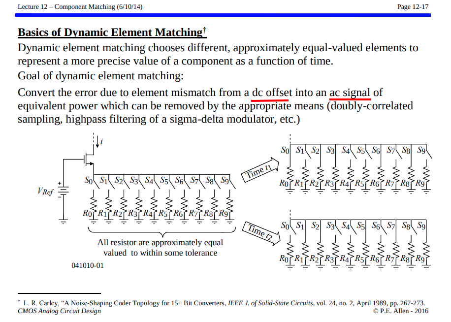
Dynamic Element Matching (DEM)
TODO 📅
Galton, Ian. (2010). Why dynamic-element-matching DACs work. Circuits and Systems II: Express Briefs, IEEE Transactions on. 57. 69 - 74. 10.1109/TCSII.2010.2042131. [https://sci-hub.se/10.1109/TCSII.2010.2042131]
KHIEM NGUYEN. Analog Devices Inc, "Practical Dynamic Element Matching Techniques for 3-level Unit Elements" [https://picture.iczhiku.com/resource/eetop/shihEDaaoJjFdCVc.pdf]
E. Alvarez-Fontecilla, P. S. Wilkins and S. C. Rose, "Understanding High-Resolution Dynamic Element Matching DACs [Feature]," in IEEE Circuits and Systems Magazine, vol. 23, no. 4, pp. 34-43, Fourthquarter 2023
E. Alvarez-Fontecilla and P. S. Wilkins, "Linearity Through Democracy [Feature]," in IEEE Circuits and Systems Magazine, vol. 25, no. 1, pp. 58-69, Firstquarter 2025
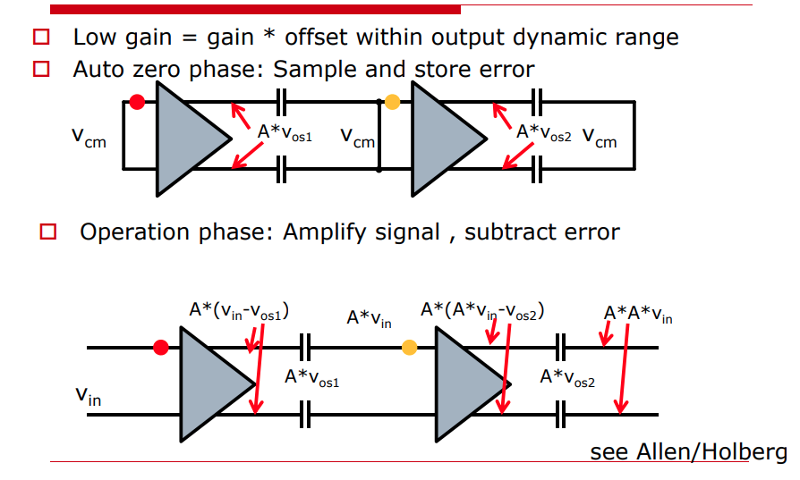
Autozeroing
offset is sampled and then subtracted from the input
Measure the offset somehow and then subtract it from the input signal
low gain comparator
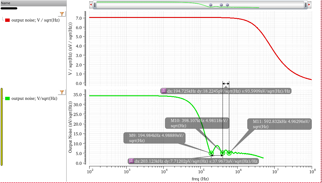
Residual Noise of Auto-zeroing
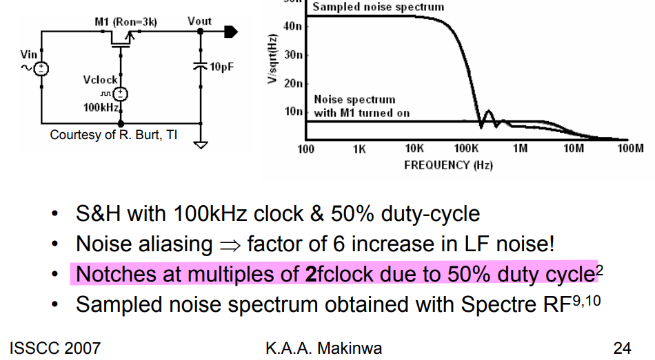
pnosie Noise Type: timeaverage
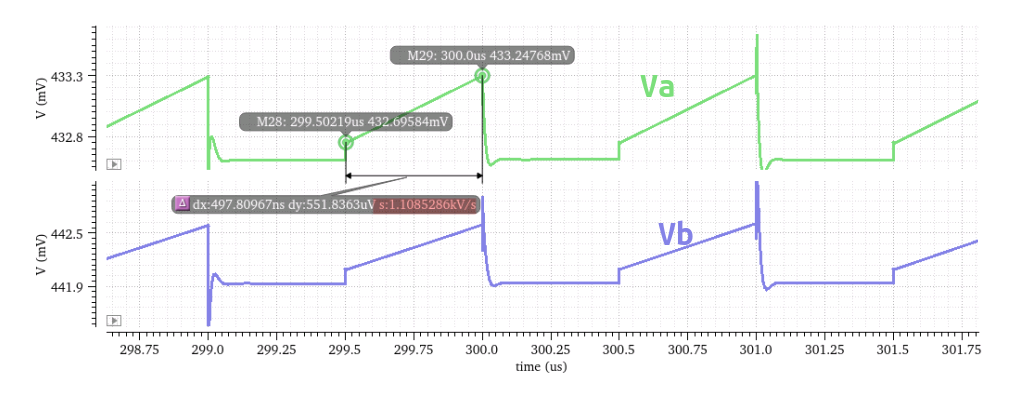
\(\Pi\)-Capacitor

\[\begin{align} (V_a-V_{a0})C_0 + (\overline{V_a - V_b} - \overline{V_{a0} - V_{b0}})C_1 &= \Delta Q_a \\ (V_b-V_{b0})C_0 + (\overline{V_b - V_a} - \overline{V_{b0} - V_{a0}})C_1 &= \Delta Q_b \end{align}\]
therefore we obtain \[\begin{align} V_a + V_b &= \frac{\Delta Q_a + \Delta Q_b}{C_0} + V_{a0} + V_{b0} \\ V_a - V_b &= \frac{\Delta Q_a - \Delta Q_b}{C_0+2C_1} + V_{a0} - V_{b0} \end{align}\] Then \[\begin{align} V_a &= \frac{\Delta Q_a(C_0+C_1)+\Delta Q_b C_1}{C_0(C_0+2C_1)} + V_{a0} \\ V_b &= \frac{\Delta Q_aC_1+\Delta Q_b (C_0+C_1)}{C_0(C_0+2C_1)} + V_{b0} \end{align}\]
rearrange the above equation \[\begin{align} V_a &= \frac{\Delta Q_a}{C_0} + \frac{\Delta Q_b-\Delta Q_a}{C_0(\frac{C_0}{C_1}+2)} + V_{a0} \\ V_b &= \frac{\Delta Q_b}{C_0} + \frac{\Delta Q_a-\Delta Q_b}{C_0(\frac{C_0}{C_1}+2)} + V_{b0} \end{align}\]
The difference between \(V_a\) and \(V_b\) \[ V_a - V_b = \frac{I_a-I_b}{C_0+2C_1}t + V_{a0} - V_{b0} \]
\(C_1\) save total capacitor area while retaining the same \(V_a - V_b\) due to \(\Delta I_{a,b}\), in comparison to \(C_0\)
at autozero phase \[\begin{align} I_{a0} &= \frac{1}{2}\mu C_{OX}\frac{W}{L}(V_{a0} - V_{TH})^2 \\ I_{Rb} &= \frac{1}{2}\mu C_{OX}\frac{W}{L}(V_{b0} - V_{TH})^2 \end{align}\]
then \[ \Delta I_0 = \frac{1}{2}(V_{a0} - V_{b0})(g_{m,a0}+g_{m,b0}) \] where \(g_{m,a0}+g_{m,b0} = \mu C_{OX}\frac{W}{L}(V_{a0}+V_{b0} - 2V_{TH})\)
at comparison phase \[\begin{align} I_{a1} &= \frac{1}{2}\mu C_{OX}\frac{W}{L}(V_{a1} - V_{TH})^2 \\ I_{b1} &= \frac{1}{2}\mu C_{OX}\frac{W}{L}(V_{b1} - V_{TH})^2 \end{align}\]
then \[ \Delta I_1 = \frac{1}{2}(V_{a1} - V_{b1})(g_{m,a1}+g_{m,b1}) \] That is, \(g_{m,a1}+g_{m,b1} = \mu C_{OX}\frac{W}{L}(V_{a1}+V_{b1} - 2V_{TH})\)
To minimize the difference between \(\Delta I_1\) and \(\Delta I_0\), the drift of both differential and common mode between \(V_a\) and \(V_b\) shall be alleviated
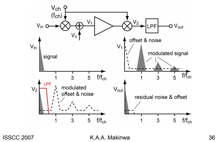
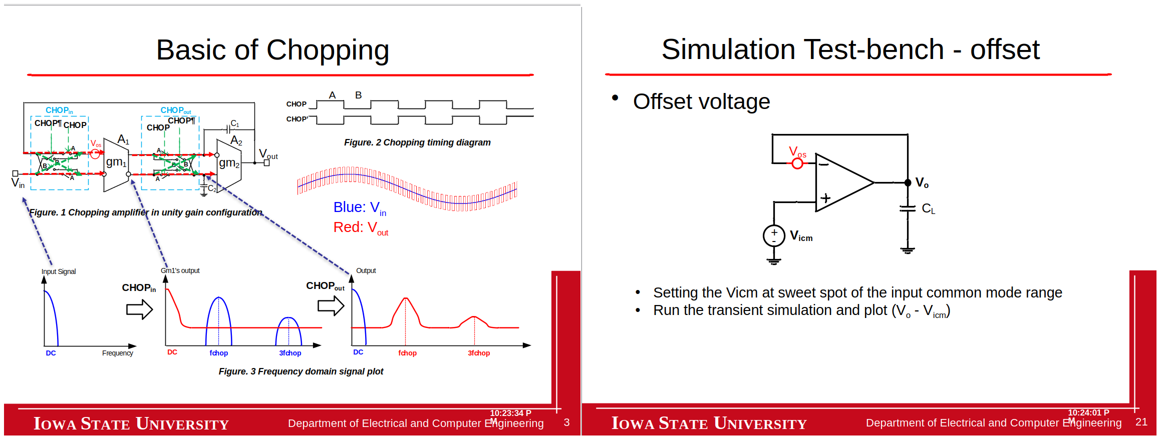
Chopping
offset is modulated away from the signal band and then filtered out
Modulate the offset away from DC and then filter it out
Good: Magically reduces offset, 1/f noise, drift
Bad: But creates switching spikes, chopper ripple and other artifacts …
Chopping in the Frequency Domain
Square-wave Modulation
definition of convolution \(y(t) = x(t)*h(t)= \int_{-\infty}^{\infty} x(\tau)h(t-\tau)d\tau\)
for real signal \(H(j\omega)^*=H(-j\omega)\)
\[ H(j\hat{\omega})*H(j\hat{\omega}) = \int_{-\infty}^{\infty}H(j\omega)H(j(\hat{\omega}-\omega))d\omega \]

The Fourier Series of squarewave \(x(t)\) with amplitudes \(\pm 1\), period \(T_0\)
\[ C_n = \left\{ \begin{array}{cl} 0 &\space \ n=0 \\ 0 &\space \ n=\text{even} \\ |\frac{2}{n\pi}| &\space n=\pm 1,\pm 5,\pm9, ... \\ -|\frac{2}{n\pi}| &\space n=\pm 3,\pm 7,\pm11, ... \end{array} \right. \]
The Fourier transform of \(s(t)=x(t)x(t)\), and we know \[\begin{align} S(j2n\omega_0) &= \frac{1}{2\pi}\int X(j(2n\omega_0 -\omega))X(j\omega) d\omega\\ &= \frac{1}{2\pi}\int X(j(\omega-2n\omega_0))X(j\omega) d\omega \end{align}\]
Therefore \(n=0\) \[ S(j0) = \frac{1}{2\pi} (2\pi)^2\cdot \frac{4}{\pi ^2}2\sum_{n=0}^{+\infty}\frac{1}{(2n+1)^2} \delta(\omega) = 2\pi \delta(\omega) \]
if \(n=1\)
\[\begin{align} S(j2\omega_0) &= \frac{1}{2\pi} (2\pi)^2\cdot \frac{4}{\pi ^2}\left(1 - 2\sum_{n=0}^{+\infty}\frac{1}{(2n+1)(2n+3)} \right) \\ &= \frac{1}{2\pi} (2\pi)^2\cdot \frac{4}{\pi ^2}\left(1 - 2\sum_{n=0}^{+\infty}\frac{1}{2}\left[\frac{1}{2n+1}- \frac{1}{2n+3}\right] \right) \\ &= 0 \end{align}\]
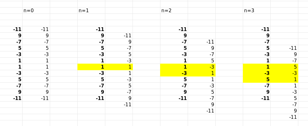
\(n=2\) \[\begin{align} \sum &= -\frac{2}{3} + 2\left(\frac{1}{1\times 5}+ \frac{1}{3\times 7}+ \frac{1}{5\times 9} + \frac{1}{7\times 11}+...\right) \\ &= -\frac{2}{3} + 2\cdot \frac{1}{4}\left(\frac{1}{1}-\frac{1}{5}+ \frac{1}{3}- \frac{1}{7}+ \frac{1}{5} - \frac{1}{9} +\frac{1}{7}-\frac{1}{11}+...\right) \\ &= -\frac{2}{3} + 2\cdot \frac{1}{4}\frac{4}{3} = 0 \end{align}\]
That is, the input signal remains the same after chopping or squarewave up/down modulation
EXAMPLE 2.7 in R. E. Ziemer and W. H. Tranter, Principles of Communications, 7th ed., Wiley, 2013 [pdf]
Prove that \(\pi^2/8 = 1 + 1/3^2 + 1/5^2 + 1/7^2 + \cdots\) [https://math.stackexchange.com/a/2348996]
Bandwidth & Gain Accuracy
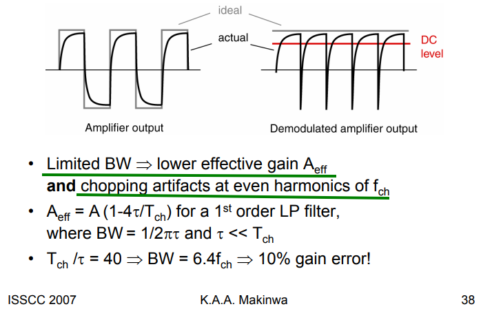
lower effective gain: DC level at the output of the amplifiers is a bit less than what it should be
chopping artifacts at the even harmonics: frequency of output is \(2f_{ch}\)
Below we justify \(A_\text{eff} = A(1-4\tau/T_\text{ch})\) \[ V_o(t) = A + (V_0-A)e^{-t/\tau} \qquad V_o(T/2) = -V_0 \]
then \[ V_0 = -A\frac{1-e^{-T/2\tau}}{1+e^{-T/2\tau}} \] Then DC level is \[ A_\text{eff} = \frac{1}{T/2}\int_0^{T/2} V_o(t)dt = A\left(1-\frac{4\tau}{T}\cdot \frac{1-e^{-T/2\tau}}{1+e^{-T/2\tau}}\right)\approx A\left(1-\frac{4\tau}{T}\right) \]
where assuming \(\tau \ll T\)
REF. [https://raytroop.github.io/2023/01/01/insight/#rc-charge-discharge]

Residual Offset of Chopping
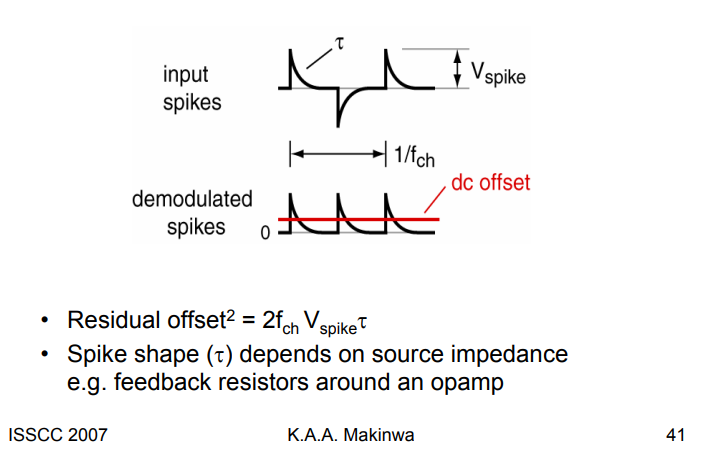
assume input spikes can be expressed as \[ V_\text{spike}(t) = V_o e^{-\frac{t}{\tau}} \]
Then, residual offset is
\[\begin{align} \overline{V_\text{os}} &= \frac{2\int_0^{T_{ch}/2}V_\text{spike}(t)dt}{T_{ch}} = 2f_{ch}V_o\int_0^{T_{ch}/2} e^{-\frac{t}{\tau}}dt = 2f_{ch}V_o\tau\int_0^{T_{ch}/2\tau} e^{-\frac{t}{\tau}}d\frac{t}{\tau}\\ &\approx 2f_{ch}V_o\tau \end{align}\]
Chopping Simulation
EE 501: CMOS Analog Integrated Circuit Design — Chopping for Offset reduction [https://class.ece.iastate.edu/djchen/ee501/2016/Chopper_design_EE501.pptx]
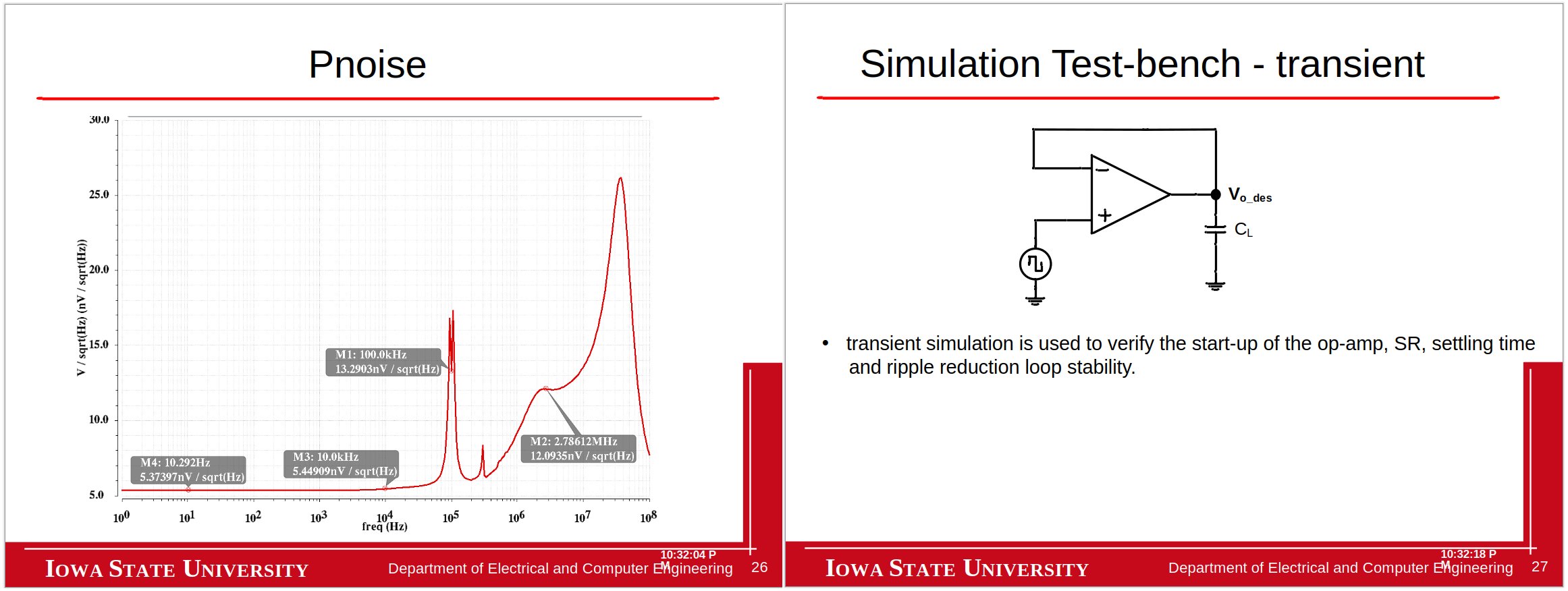
- Run transient simulation to ensure the amp output can settle into a steady-state and offset ripple is small
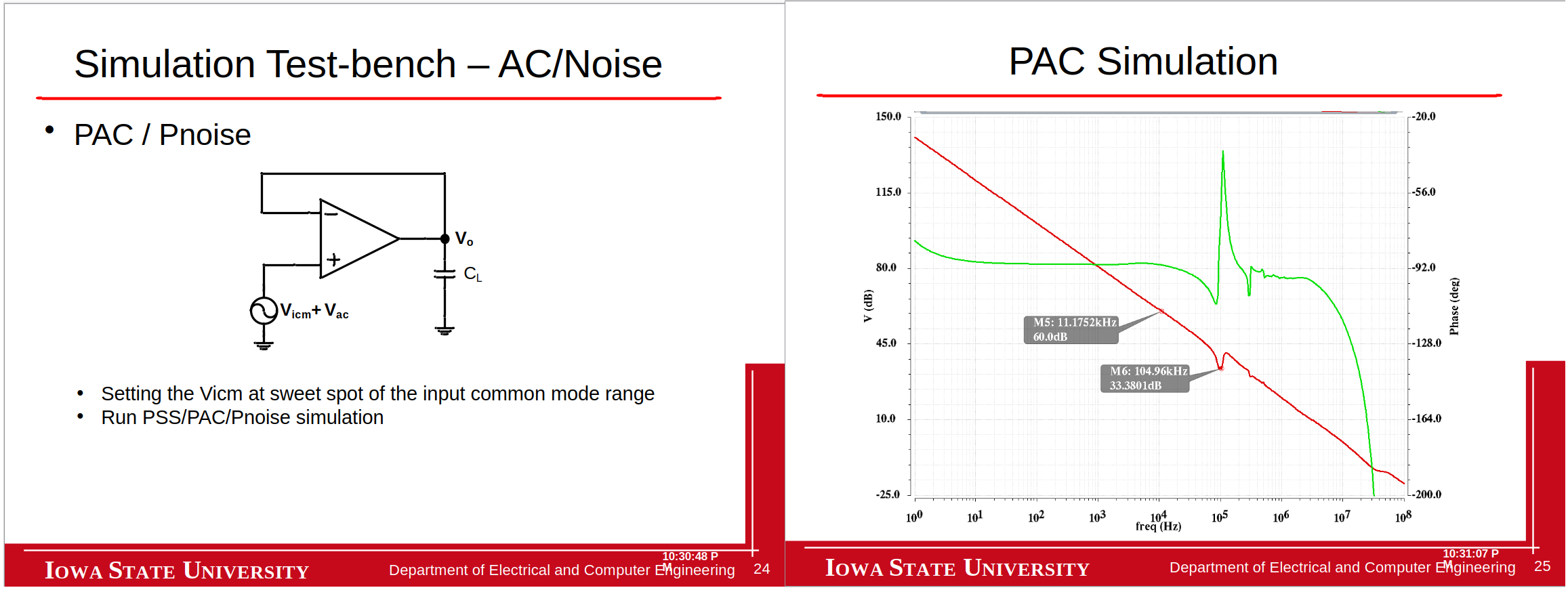
- Run PAC/ Pnoise to verify the ac and noise performance with chopping on
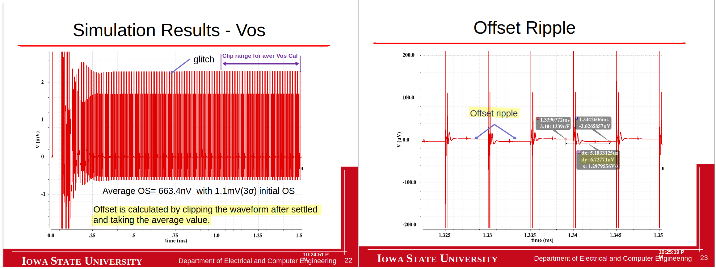
Ripple Cancellation after Chopping
On-chip analog filter is not good enough due to limited cutoff frequency

at \(\Phi_+\) phase \[ \left\{ \begin{array}{cl} \Delta V_\text{os}[n] &= \frac{I_l[n]-I_r[n-1]}{G_m} \\ \left(I_0+\frac{V_\text{os0}-\Delta V_\text{os}[n]}{R_E}\right)\beta &= I_l[n]+I_r[n-1] \end{array} \right. \] Then \[ \left\{ \begin{array}{cl} I_r[n-1] &= \frac{-G_mR_E-\beta}{2R_E}\cdot \Delta V_\text{os}[n] + \frac{\beta}{2R_E}V_\text{os0}+\frac{\beta}{2}I_0 \\ I_l[n] &= \frac{G_mR_E-\beta}{2R_E}\cdot \Delta V_\text{os}[n] + \frac{\beta}{2R_E}V_\text{os0}+\frac{\beta}{2}I_0 \end{array} \right. \] at \(\Phi_-\) phase \[ \left\{ \begin{array}{cl} \Delta V_\text{os}[n] &= \frac{I_l[n-1]-I_r[n]}{G_m} \\ \left(I_0+\frac{-V_\text{os0}+\Delta V_\text{os}[n]}{R_E}\right)\beta &= I_l[n-1]+I_r[n] \end{array} \right. \] Then \[ \left\{ \begin{array}{cl} I_r[n] &= \frac{-G_mR_E+\beta}{2R_E}\cdot \Delta V_\text{os}[n] - \frac{\beta}{2R_E}V_\text{os0}+\frac{\beta}{2}I_0 \\ I_l[n-1] &= \frac{G_mR_E+\beta}{2R_E}\cdot \Delta V_\text{os}[n] - \frac{\beta}{2R_E}V_\text{os0}+\frac{\beta}{2}I_0 \end{array} \right. \] \(\Phi_+ \to \Phi_-\) state transformation \[ \left\{ \begin{array}{cl} I_r[n-1] &= \frac{-G_mR_E-\beta}{2R_E}\cdot \Delta V_\text{os}[n] + \frac{\beta}{2R_E}V_\text{os0}+\frac{\beta}{2}I_0 \\ I_l[n] &= \frac{G_mR_E-\beta}{2R_E}\cdot \Delta V_\text{os}[n] + \frac{\beta}{2R_E}V_\text{os0}+\frac{\beta}{2}I_0 \end{array} \right. \to \left\{ \begin{array}{cl} I_r[n+1] &= \frac{-G_mR_E+\beta}{2R_E}\cdot \Delta V_\text{os}[n+1] - \frac{\beta}{2R_E}V_\text{os0}+\frac{\beta}{2}I_0 \\ I_l[n] &= \frac{G_mR_E+\beta}{2R_E}\cdot \Delta V_\text{os}[n+1] - \frac{\beta}{2R_E}V_\text{os0}+\frac{\beta}{2}I_0 \end{array} \right. \] Two \(I_l[n]\) shall be equal, that is \[ \frac{G_mR_E-\beta}{2R_E}\cdot \Delta V_\text{os}[n] + \frac{\beta}{2R_E}V_\text{os0}+\frac{\beta}{2}I_0 = \frac{G_mR_E+\beta}{2R_E}\cdot \Delta V_\text{os}[n+1] - \frac{\beta}{2R_E}V_\text{os0}+\frac{\beta}{2}I_0 \] Rearrange the above equation \[ \Delta V_\text{os}[n+1] = \frac{G_mR_E-\beta}{G_mR_E+\beta}\Delta V_\text{os}[n] + \frac{2\beta}{G_mR_E+\beta}V_\text{os0} \] \(\Phi_- \to \Phi_+\) state transformation \[ \left\{ \begin{array}{cl} I_r[n] &= \frac{-G_mR_E+\beta}{2R_E}\cdot \Delta V_\text{os}[n] - \frac{\beta}{2R_E}V_\text{os0}+\frac{\beta}{2}I_0 \\ I_l[n-1] &= \frac{G_mR_E+\beta}{2R_E}\cdot \Delta V_\text{os}[n] - \frac{\beta}{2R_E}V_\text{os0}+\frac{\beta}{2}I_0 \end{array} \right. \to \left\{ \begin{array}{cl} I_r[n] &= \frac{-G_mR_E-\beta}{2R_E}\cdot \Delta V_\text{os}[n+1] + \frac{\beta}{2R_E}V_\text{os0}+\frac{\beta}{2}I_0 \\ I_l[n+1] &= \frac{G_mR_E-\beta}{2R_E}\cdot \Delta V_\text{os}[n+1] + \frac{\beta}{2R_E}V_\text{os0}+\frac{\beta}{2}I_0 \end{array} \right. \] Two \(I_r[n]\) shall be equal, that is \[ \frac{-G_mR_E+\beta}{2R_E}\cdot \Delta V_\text{os}[n] - \frac{\beta}{2R_E}V_\text{os0}+\frac{\beta}{2}I_0 = \frac{-G_mR_E-\beta}{2R_E}\cdot \Delta V_\text{os}[n+1] + \frac{\beta}{2R_E}V_\text{os0}+\frac{\beta}{2}I_0 \] Rearrange the above equation \[ \Delta V_\text{os}[n+1] = \frac{G_mR_E-\beta}{G_mR_E+\beta}\Delta V_\text{os}[n] + \frac{2\beta}{G_mR_E+\beta}V_\text{os0} \]
Both State-transition equations are same \[ \Delta V_\text{os}[n+1] = \frac{G_mR_E-\beta}{G_mR_E+\beta}\Delta V_\text{os}[n] + \frac{2\beta}{G_mR_E+\beta}V_\text{os0} \] With geometric progression sum formula \[ \Delta V_\text{os}[n] = \left(\frac{G_mR_E-\beta}{G_mR_E+\beta}\right)^n\cdot \Delta V_\text{os}[0] + \left[1-\left(\frac{G_mR_E-\beta}{G_mR_E+\beta}\right)^n\right]\cdot V_\text{os0} \] during \(n \to \infty\) \[ \lim_{n\to \infty} \Delta V_\text{os}[n] = V_\text{os0} \] As expected \[ \lim_{n\to \infty} V_\text{os}[n] =\lim_{n\to \infty} V_\text{os0}-\Delta V_\text{os}[n] = 0 \]
Assuming that begainning from \(\Phi_+\) phase \[ \left\{ \begin{array}{cl} \Delta V_\text{os}[0] &= \frac{I_l[0]-I_r[-1]}{G_m} \\ \left(I_0+\frac{V_\text{os0}-\Delta V_\text{os}[0]}{R_E}\right)\beta &= I_l[0]+I_r[-1] \end{array} \right. \overset{\mathcal{I_r[-1]=0}}{\Longrightarrow} \Delta V_\text{os}[0]=\frac{(I_0R_E+V_\text{os0})\beta}{G_mR_E+\beta} \] With \(I_0=10\mu A\), \(R_E=5k \Omega\), \(V_\text{os0}=20mV\), \(G_m=500\mu S\), \(\beta=0.5\) \[ \left\{ \begin{array}{cl} \Delta V_\text{os}[0] &= 167mV \\ \frac{G_mR_E-\beta}{G_mR_E+\beta} &= 0.667 \end{array} \right. \]
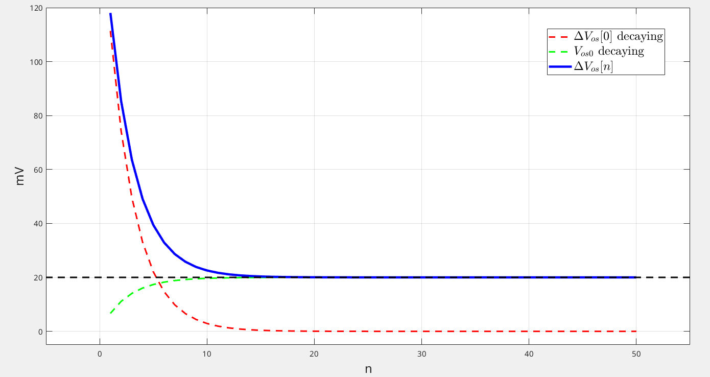
1 | DVos0 = 167; % mV |
reference
C. C. Enz and G. C. Temes, "Circuit techniques for reducing the effects of op-amp imperfections: autozeroing, correlated double sampling, and chopper stabilization," in Proceedings of the IEEE, vol. 84, no. 11, pp. 1584-1614, Nov. 1996, doi: 10.1109/5.542410. [http://www2.ing.unipi.it/~a008309/mat_stud/MIXED/archive/2019/Articles/Offset_canc_Enz_Temes_96.pdf]
R. Gregorian and G. C. Temes. Analog MOS Integrated Circuits for Signal Processing. Wiley-Interscience, 1986 [pdf]
Christian-Charles Enz. "High precision CMOS micropower amplifiers" [pdf]
Kofi Makinwa. Precision Analog Circuit Design: Coping with Variability, [https://youtu.be/nA_DZtRqrTQ] [https://youtu.be/uwRpP20Lprc]
Chung-chun Chen, Why Design Challenge in Chopping Offset & Flicker Noise? [https://youtu.be/ydjca2KrXgc]
—, Why Needs A Low Ripple after Chopping Amplifier for A Very Low DC Offset & Flicker Noise? [https://youtu.be/y7TzJtHE7IA]
Qinwen Fan, Evolution of precision amplifiers
Kofi Makinwa, ISSCC 2007 Dynamic-Offset Cancellation Techniques in CMOS [https://picture.iczhiku.com/resource/eetop/sYkywlkpwIQEKcxb.pdf]
Axel Thomsen, Silicon Laboratories ISSCC2012 T8: "Managing Offset and Flicker Noise" [slides,transcript]
P. Bruschi, Dynamic techniques for the rejection of the offset and low frequency noise [https://docenti.ing.unipi.it/~a008309/mat_stud/MIXED/2023/Lecture_notes/Chap_2_2_Offset_Flicker_Reduction.pdf]
CC Chen. Why Dynamic Offset or Mismatch Cancellation with Auto-zeroing Technique? [https://youtu.be/PQJwzd1tyO0]
—. Why Dynamic Offset or Mismatch Cancellation with Chopping Technique? [https://youtu.be/x5FS8jEKu_g]
—. Why Design Challenge in Chopping Offset & Flicker Noise? [https://youtu.be/ydjca2KrXgc]
—. Why Needs A Low Ripple after Chopping Amplifier for A Very Low DC Offset & Flicker Noise? [https://youtu.be/y7TzJtHE7IA]
Qinwen Fan, Kofi Makinwa. IEEE Sensors 2018: Capacitively-Coupled Chopper Instrumentation Amplifiers : an Overview [https://youtu.be/NoGHJfCFCks]