Delta-Sigma Modulator
Classification
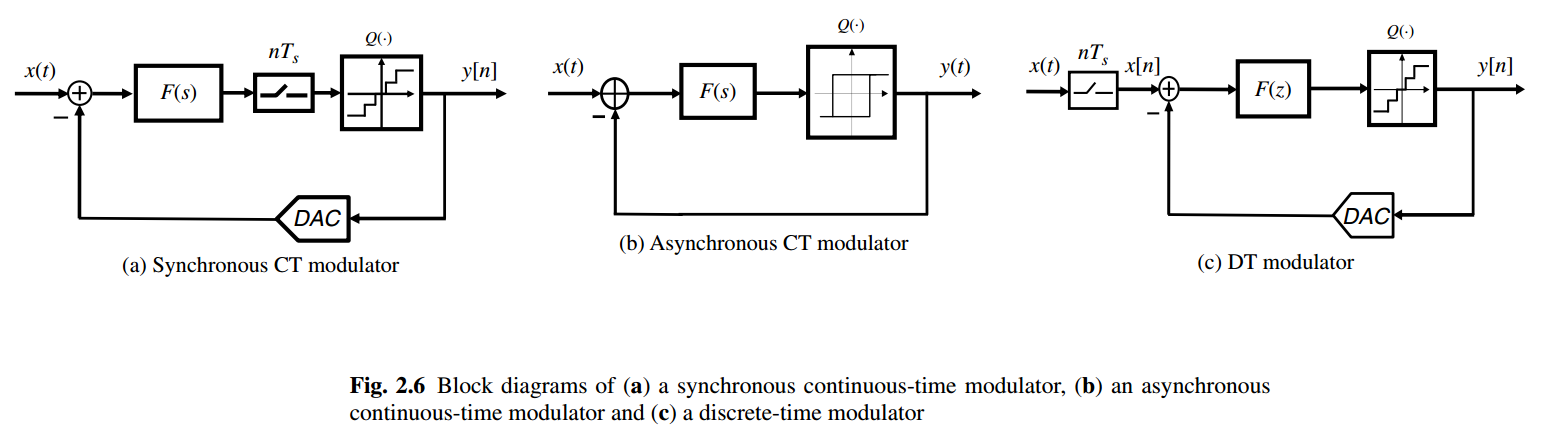
- Continuous-Time (CT) Analog Modulator
- Sampled Quantizer: Synchronous Modulator
- Unsampled Quantizer: Asynchronous Modulator
- Discrete-Time (DT) Analog Modulator
- The main application is in \(\Delta\Sigma\) ADCs
- Discrete-Time Digital Modulators (DDSM)
- Single Quantizer DDSMs - output feedback
- Error feedback modulators (EFM) - error feedback
- Multi stAge noise SHaping (MASH)
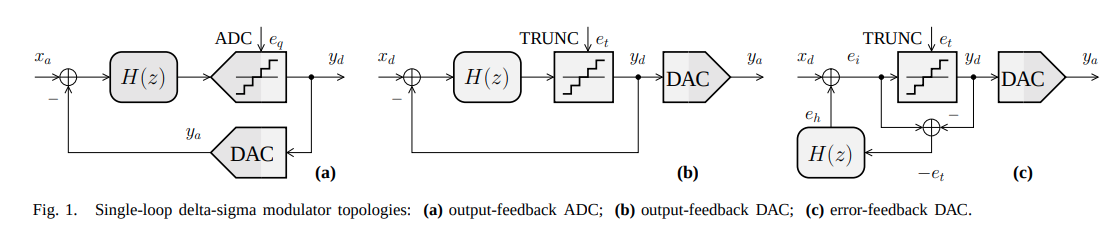
"Quantizers" and "truncators", and "integrators" and "accumulators" are used in delta-sigma ADCs and DACs, respectively
P. Kiss, J. Arias and Dandan Li, "Stable high-order delta-sigma DACS," 2003 IEEE International Symposium on Circuits and Systems (ISCAS), Bangkok, 2003 [https://www.ele.uva.es/~jesus/analog/tcasi2003.pdf]
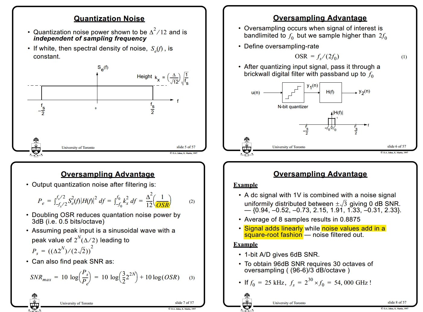
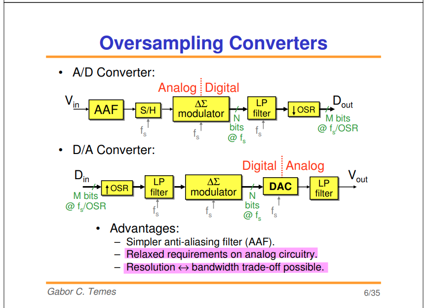
Oversampling
David Johns and Ken Martin. Oversampling Converters [https://www.eecg.toronto.edu/~johns/ece1371/slides/14_oversampling.pdf]
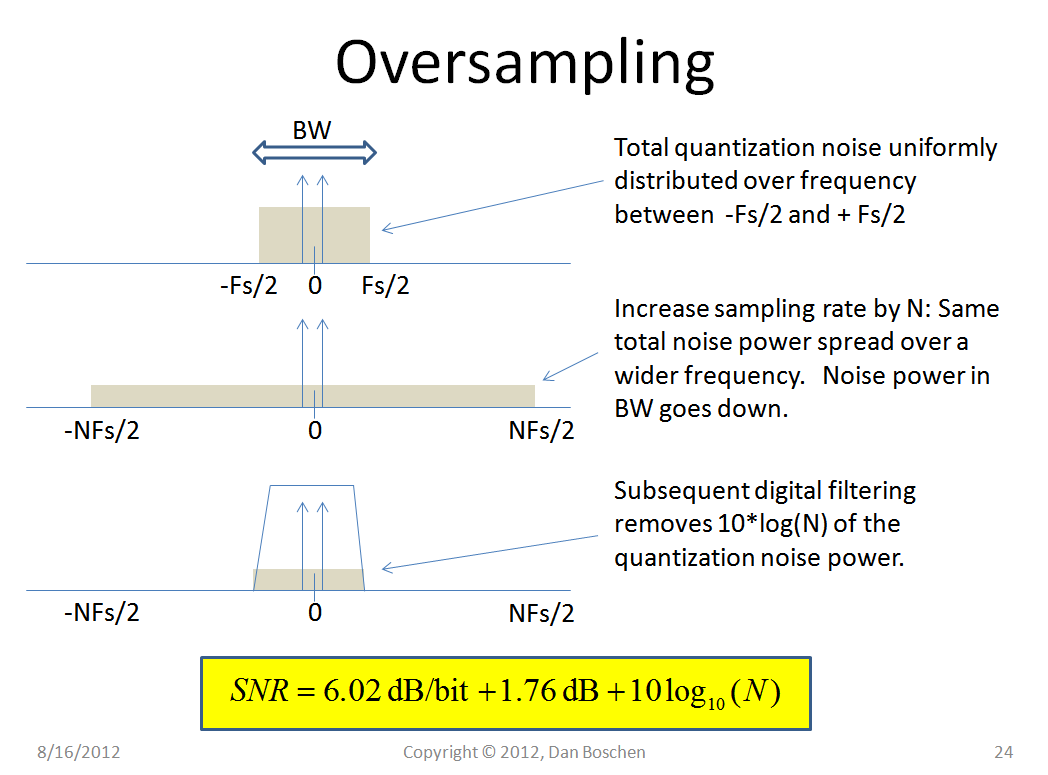
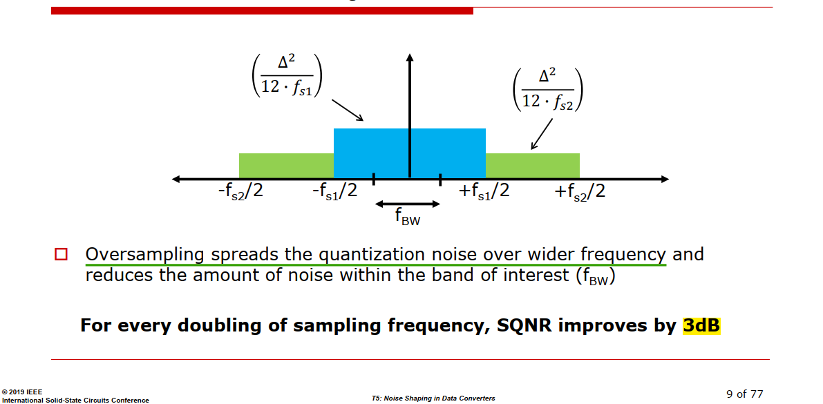
Nyquist sampling theorem @signal: no aliasing, signal remain the same
noise folding @noise: same total noise power spread over a wider frequency
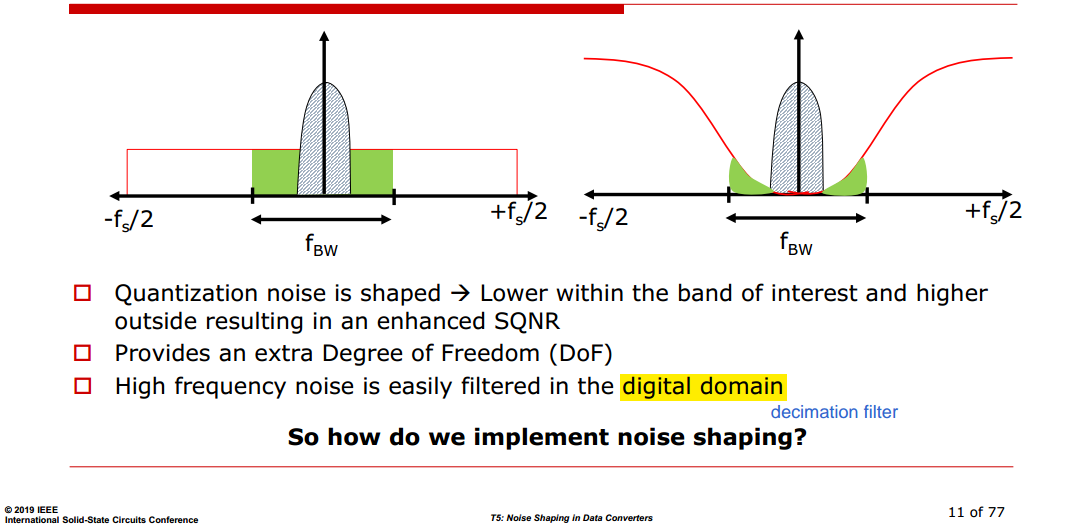
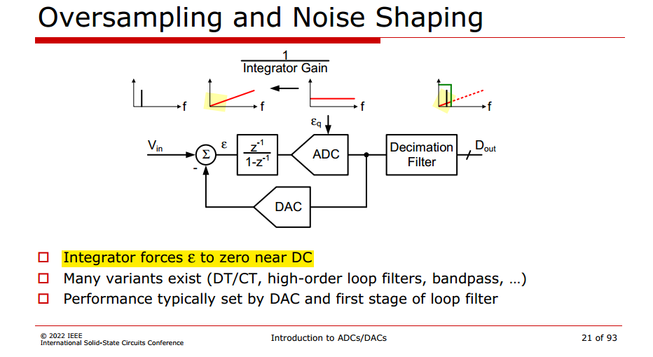
Noise Shaping
1 | [h1, w1] = freqz([1 -1], 1); |
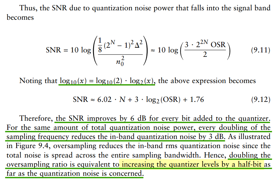
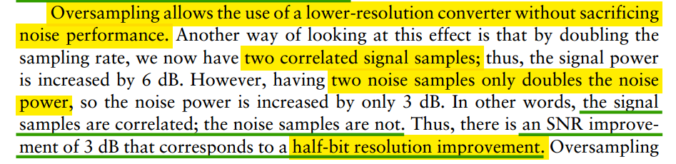
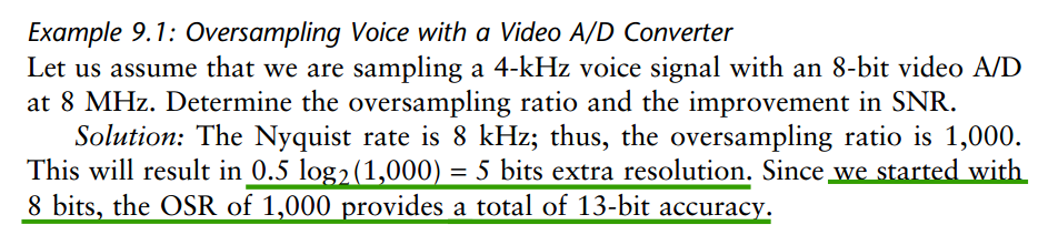
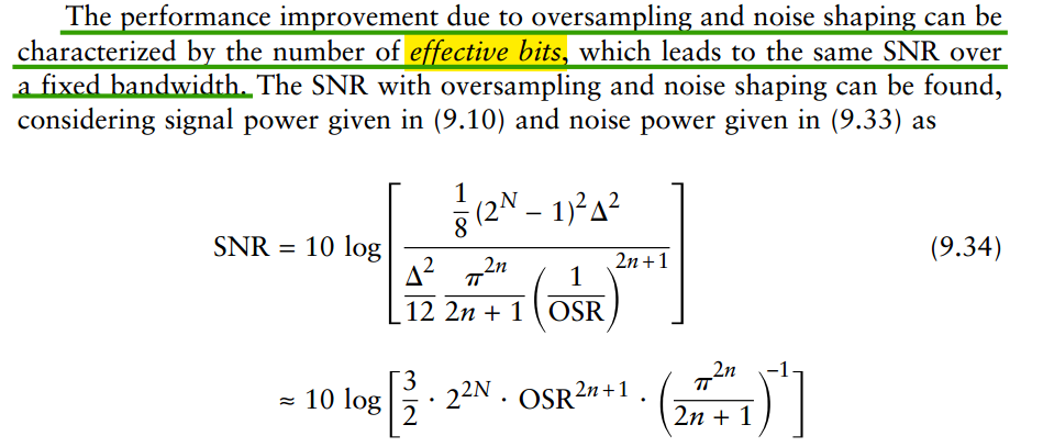
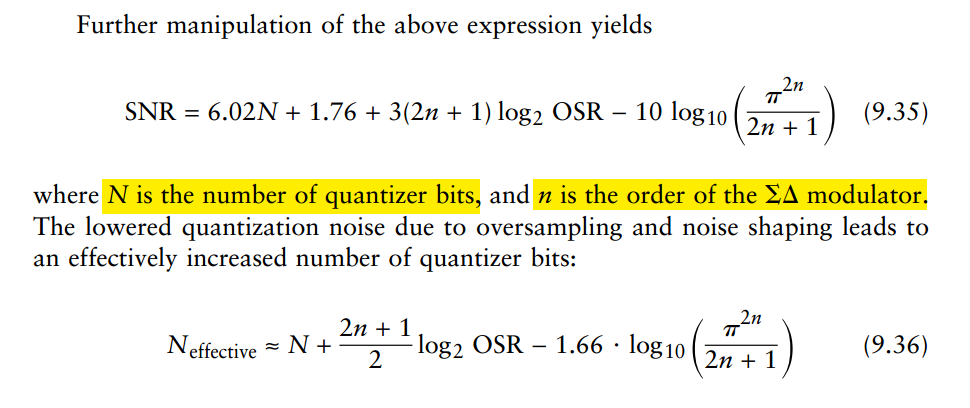
SQNR improvement
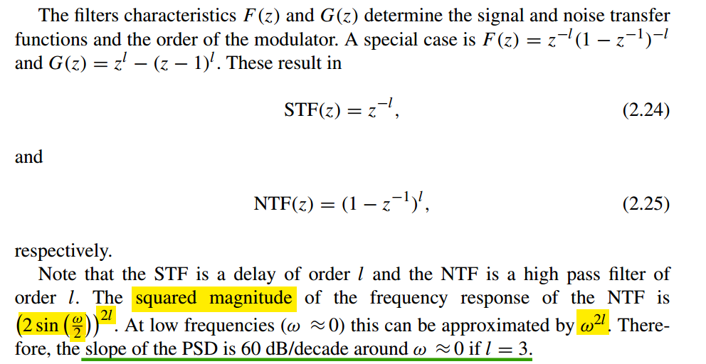
In general, for an \(l\)th order modulator with \(\text{NTF}(z) = (1 − z^{−1})^l\), the SQNR increases by \((6l + 3)\) dB for every doubling of the OSR, which provides \(l+0.5\) extra bits resolution
without the delta-sigma loop
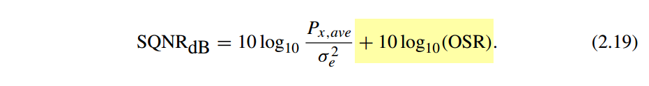
\(10\log (2) \approx 3\)dB
first order delta-sigma modulator
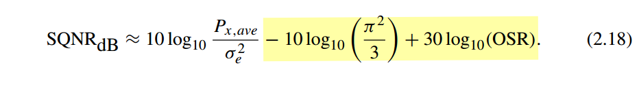
\(30\log (2) \approx 9\)dB
second order delta-sigma modulator
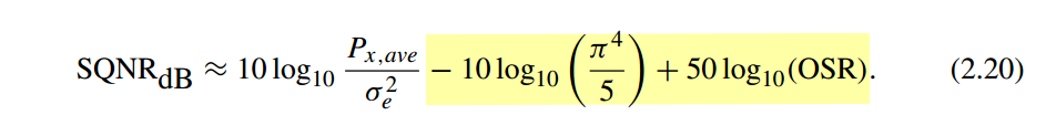
\(50\log (2) \approx 15\)dB
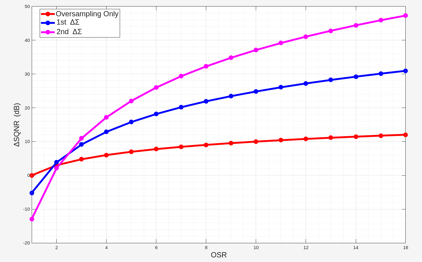
1 | OSR= linspace(1,16,16); |
TI. ADC12EU050 Continuous-Time Sigma-Delta ADCs [https://www.ti.com/lit/an/snaa098/snaa098.pdf]
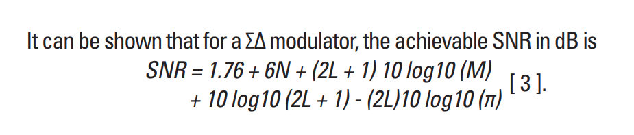
where \(N\) is the number of bits in the output, \(M\) is known as the over-sampling ratio, \(L\) is loop orders
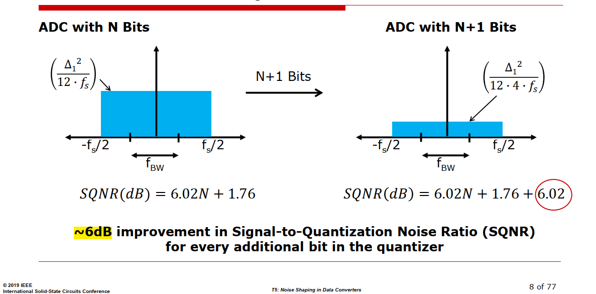
Quantizer Bits & ENOB
without the delta-sigma loop
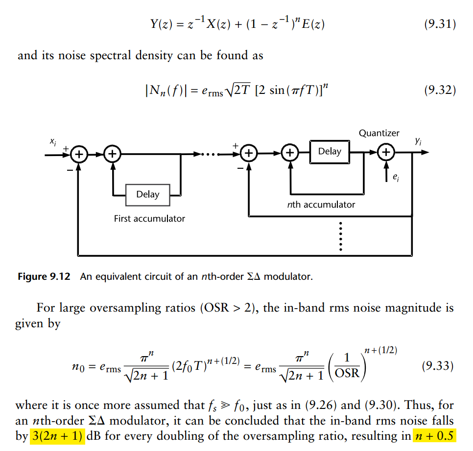
High-Order \(\Delta\Sigma\) Modulators
The greater the number of quantizer levels, the smaller quantization error
Performance Metrics
- signal-to-noise ratio (SNR)
- dynamic range (DR)
- signal-to-(noise + distortion) ratio (SNDR)
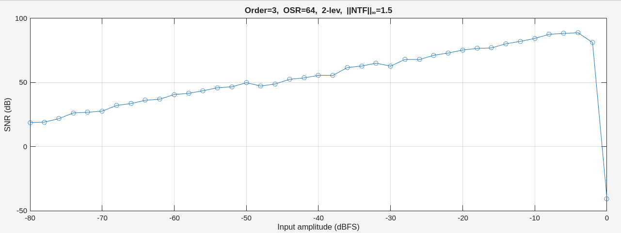
DR by "SNR Max" Definition (\(\Delta\Sigma\) Specific)
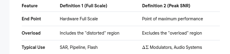
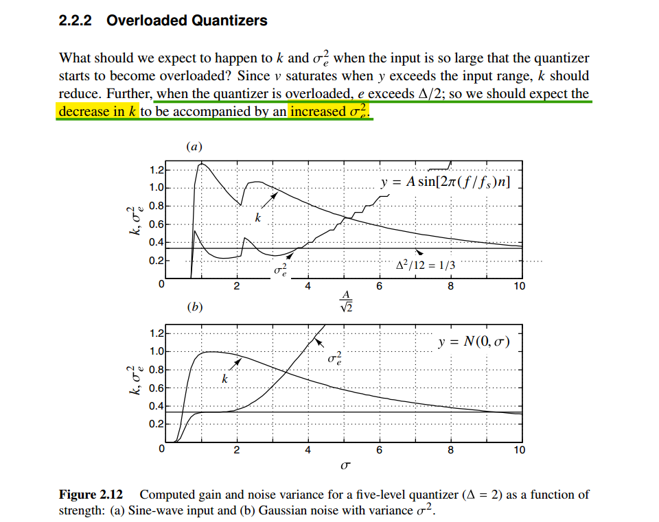
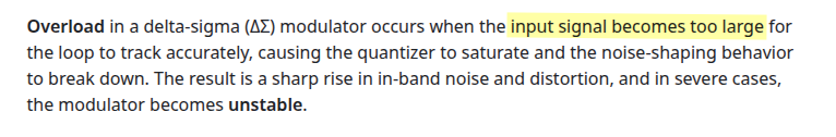
Quantizer overload
M. Neitola, "Lee's Rule Extended," in IEEE Transactions on Circuits and Systems II: Express Briefs, vol. 64, no. 4, pp. 382-386, April 2017
Maximum Stable Amplitude (MSA)
1 | % Schreier Delta-Sigma Toolbox required |
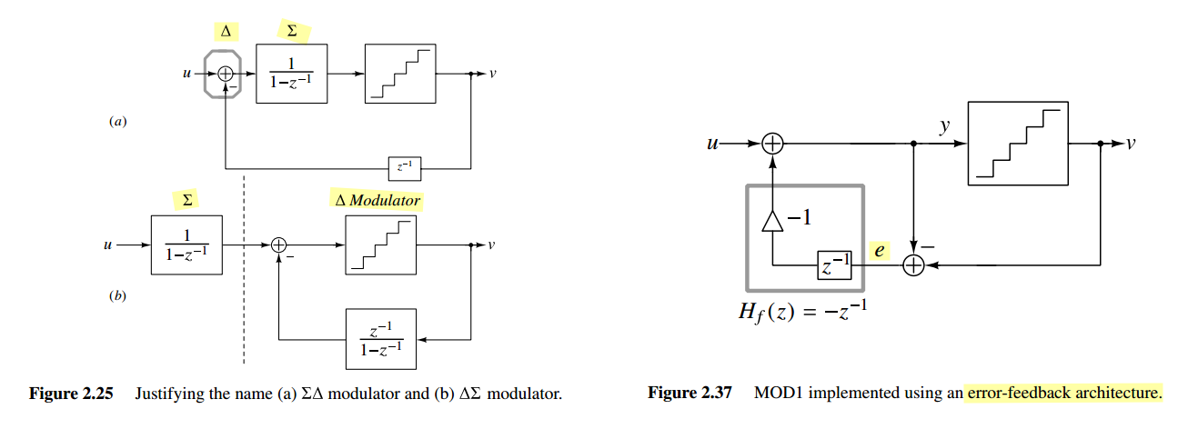
\(\Delta \Sigma\) vs. \(\Delta\) modulation
\(\Delta \Sigma\) modulators, and other noise-shaping modulators, change the spectrum of the noise but leave the signal unchanged
\(\Delta\) modulators and other signal-predicting modulators shape the spectrum of the modulated signal but leave the quantization noise unchanged at the receiver
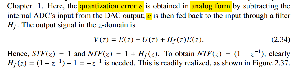
output vs. error-feedback
The error-feedback architecture is problematic for analog implementation, since it is sensitive to variations of its parameters (subtractor realization)
- The error-feedback structure is thus of limited utility in \(\Delta \Sigma\) ADCs
- The error-feedback structure is very useful and applied in digital loops required in \(\Delta \Sigma\) DACs
ADC
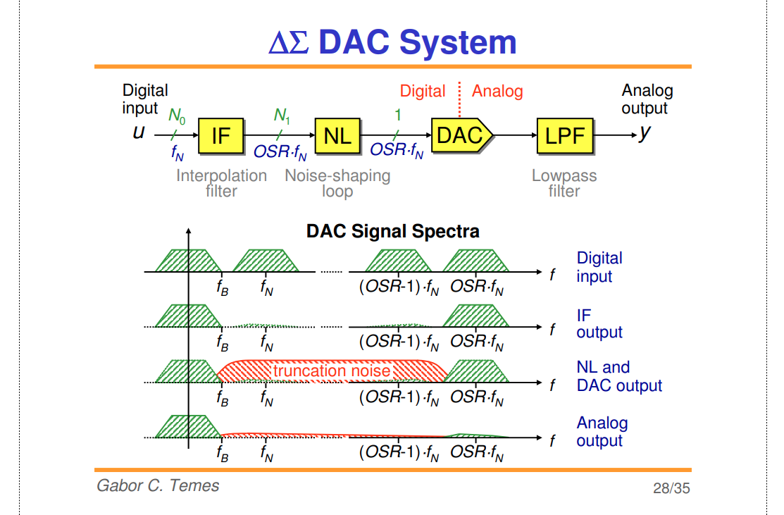
DAC
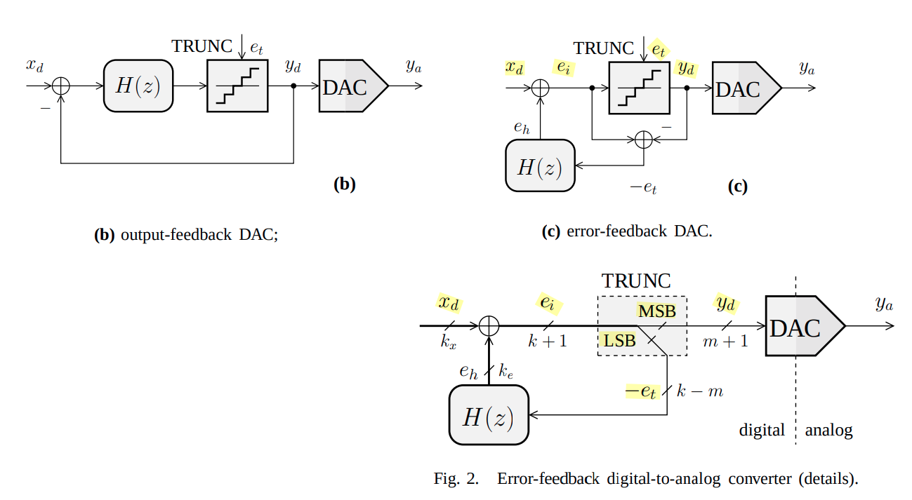
P. Kiss, J. Arias and Dandan Li, "Stable high-order delta-sigma DACS," 2003 IEEE International Symposium on Circuits and Systems (ISCAS), Bangkok, 2003 [https://www.ele.uva.es/~jesus/analog/tcasi2003.pdf]
output-feedback
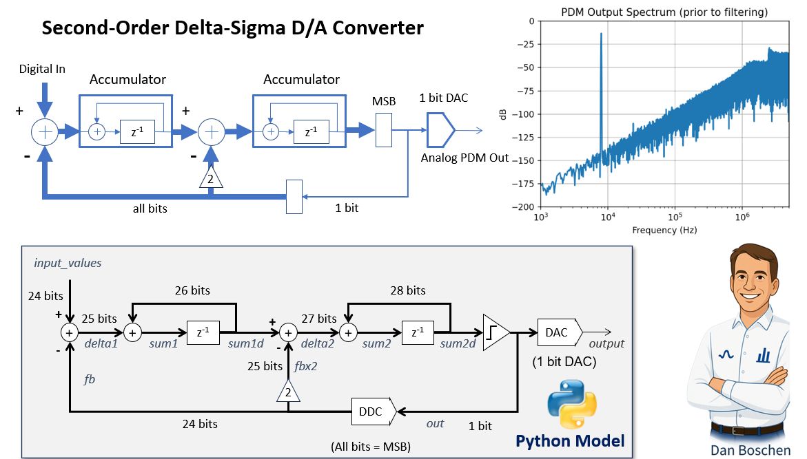
1 | // https://github.com/hamsternz/second_order_sigma_delta_DAC |
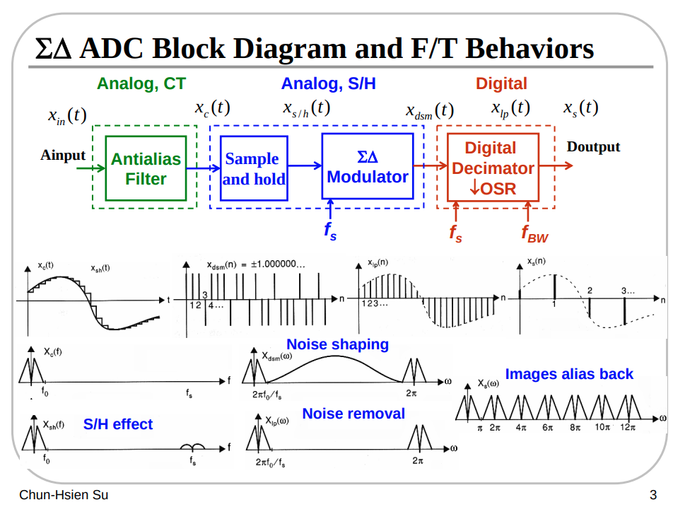
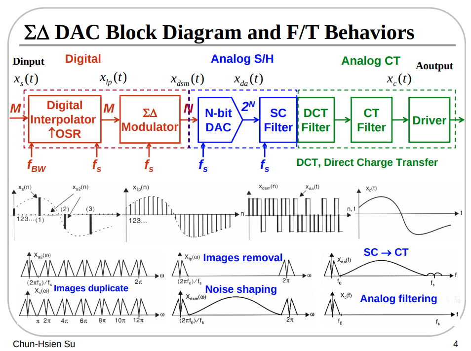
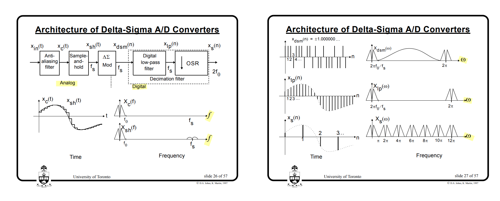
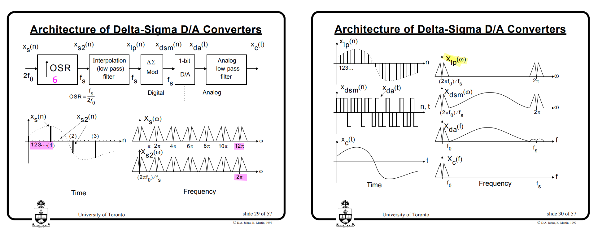
Time and Frequency Domain
\(M \gt N\)
Chun-Hsien Su ( 蘇純賢). Fundamentals of Sigma-Delta Data Converters,July, 2006 [pdf]
ADC
hackaday. Tearing Into Delta Sigma ADC’s [https://hackaday.com/2016/07/07/tearing-into-delta-sigma-adcs-part-1/]
DAC
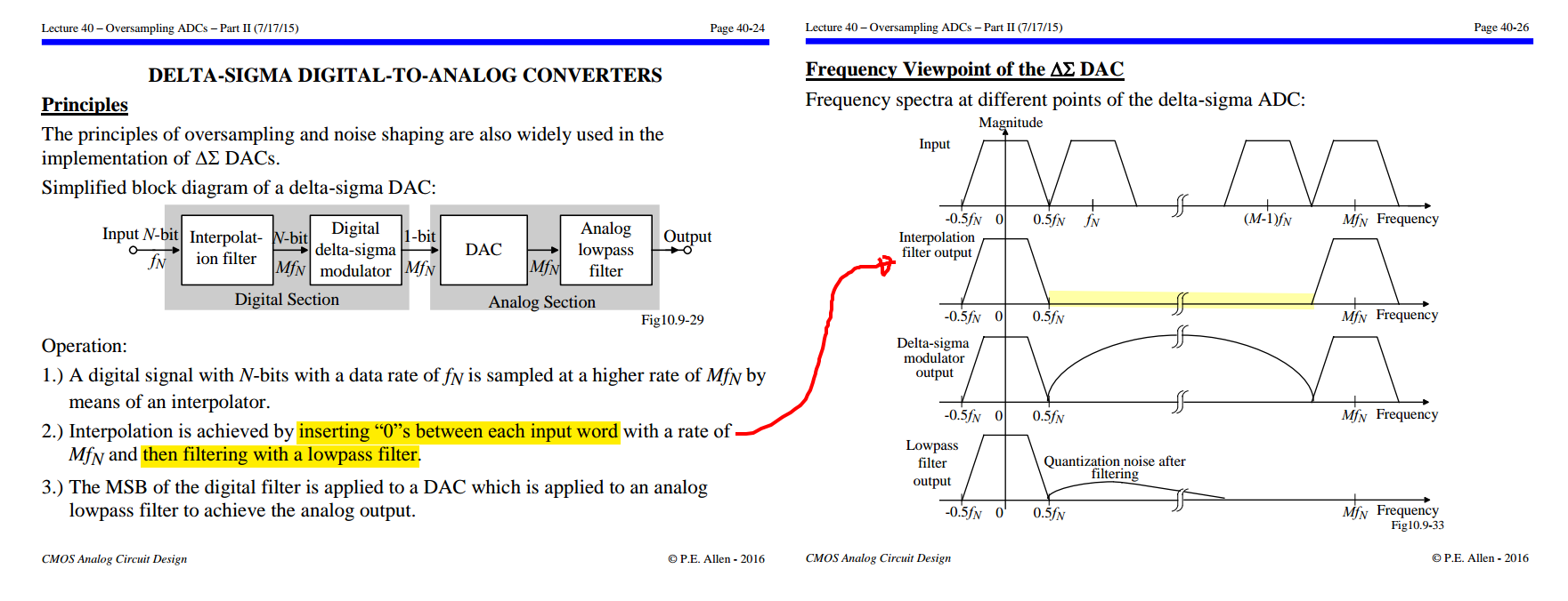
an interpolation filter effectively up-samples its low-rate input and lowpass-filters the resulting high-rate data to produce a high-rate output devoid of images
P.E. Allen -CMOS Analog Circuit Design: Lecture 39 – Oversampling ADCs – Part I (6/26/14) [https://aicdesign.org/wp-content/uploads/2018/08/lecture39-140626.pdf]
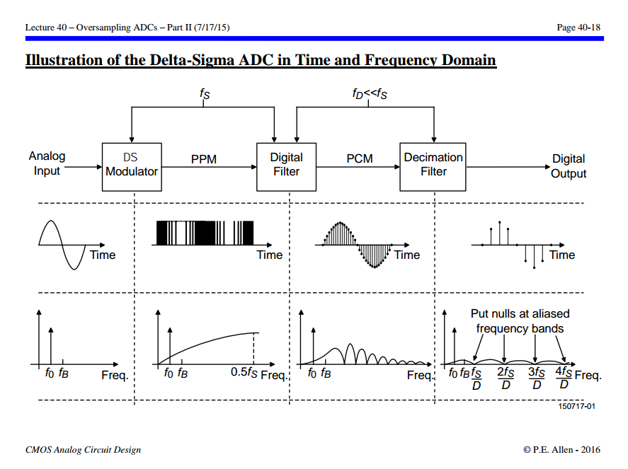
P.E. Allen -CMOS Analog Circuit Design: Lecture 40 – Oversampling ADCs – Part II (7/17/15) [https://aicdesign.org/wp-content/uploads/2018/08/lecture40-150717.pdf]
David Johns and Ken Martin. Oversampling Converters [https://www.eecg.toronto.edu/~johns/ece1371/slides/14_oversampling.pdf]
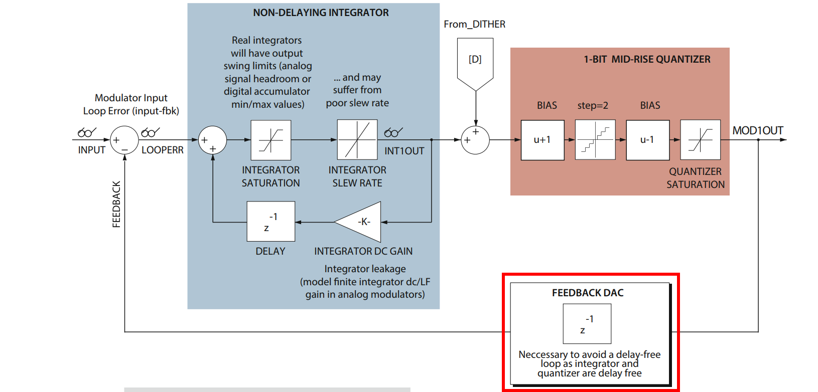
No delay-free loops
Any such physically feasible device will take a finite time to operate – in other words, the quantized output will only be available a small time after the quantizer has "looked" at the input - insert a one-sample delay
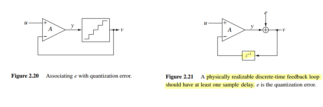
there cannot be a "delay free loop" is a common idea in sequential digital state machine design
Both integrator and quantizer are delay free
NTF realizability criterion: No delay-free loops in the modulator
linear settling & GBW of amplifier
TODO 📅
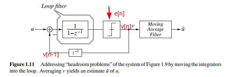
Switched capacitor has been the common realization technique of discrete-time (DT) modulators, and in order to achieve a linear settling, the sampling frequency used in these converters needs to be significantly lower than the gain bandwidth product (GBW) of the amplifiers.
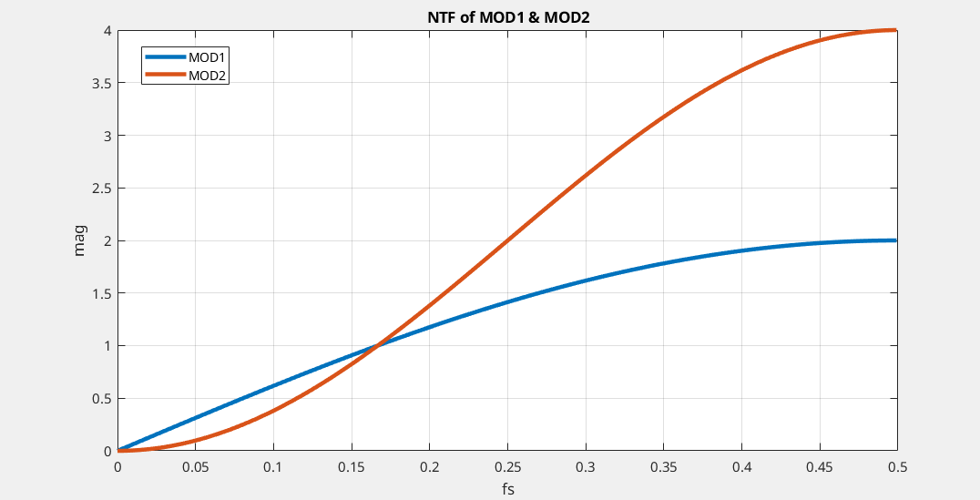
MOD1 & MOD2
MOD1: first-order noise-shaped converter (\(\Delta\Sigma\) modulator)
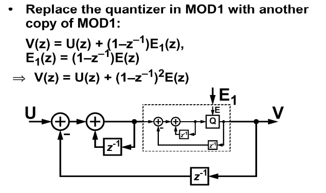
MOD2: second-order noise-shaped converter (\(\Delta\Sigma\) modulator)
MOD1
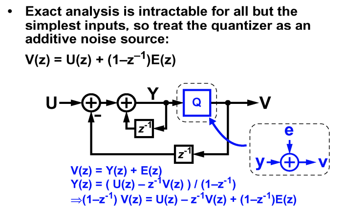 \[
V(z) = U(z) +(1-z^{-1})E(z)
\]
\[
V(z) = U(z) +(1-z^{-1})E(z)
\]
- A binary DAC (and hence a binary modulator) is inherently linear
- With a CT loop filter, MOD1 has inherent anti-alising
 \[\begin{align}
v[1] &= u - (0) + e[1] \\
v[2] &= 2u - (v[1]) + e[2] \\
v[3] &= 3u - (v[1]+v[2]) + e[3] \\
v[4] &= 4u - (v[1]+v[2]+v[3]) + e[4]
\end{align}\]
\[\begin{align}
v[1] &= u - (0) + e[1] \\
v[2] &= 2u - (v[1]) + e[2] \\
v[3] &= 3u - (v[1]+v[2]) + e[3] \\
v[4] &= 4u - (v[1]+v[2]+v[3]) + e[4]
\end{align}\]
That is \[ v[n] = nu - \sum_{k=1}^{n-1}v[k] + e[n] \] Therefore, we have \(v[n-1] = (n-1)u - \sum_{k=1}^{n-2}v[k] + e[n-1]\), then \[\begin{align} v[n] &= nu - \sum_{k=1}^{n-1}v[k] + e[n] \\ &= u + \left((n-1)u - \sum_{k=1}^{n-2}v[k]\right) - v[n-1] + e[n] \\ &= u + v[n-1] - e[n-1] -v[n-1] + e[n] \\ &= u + e[n] - e[n-1] \end{align}\]
Dout, the low frequency component of ADC out is same with Vin
MOD2
[https://web.engr.oregonstate.edu/~temes/ece627/Lecture_Notes/2nd_Higher_Order.pdf]
MOD1 with DC Excitation
TODO 📅
Mismatch Shaping
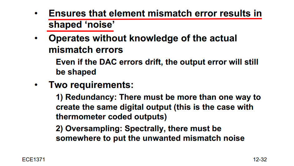
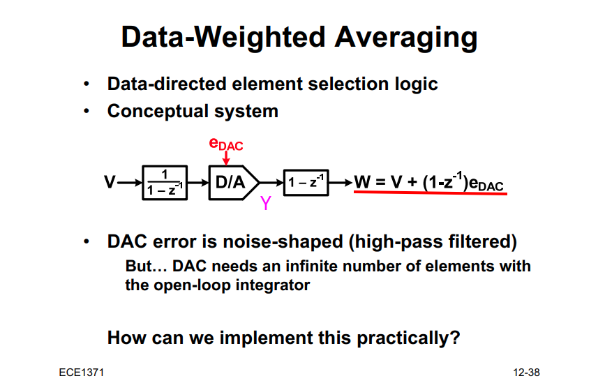
Data-Weighted Averaging (DWA)
 \[\begin{align}
\sum_{i=0}^{n}v[i] + e_\text{DAC}[n] &= y[n] \\
\sum_{i=0}^{n-1}v[i] + e_\text{DAC}[n-1] &= y[n-1]
\end{align}\]
\[\begin{align}
\sum_{i=0}^{n}v[i] + e_\text{DAC}[n] &= y[n] \\
\sum_{i=0}^{n-1}v[i] + e_\text{DAC}[n-1] &= y[n-1]
\end{align}\]
and we have \(w[n] = y[n] - y[n-1]\), then \[ w[n] = v[n] + e_\text{DAC}[n] - e_\text{DAC}[n-1] \] i.e. \[ W = V + (1-z^{-1})e_\text{DAC} \]
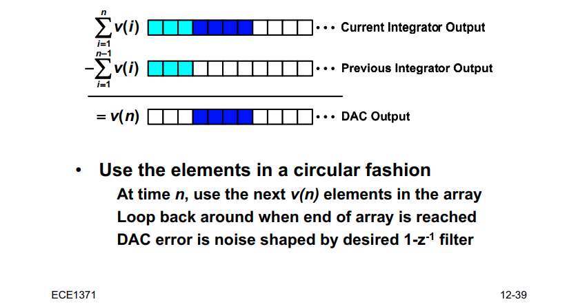
Element Rotation:
[http://individual.utoronto.ca/schreier/lectures/12-2.pdf], [http://individual.utoronto.ca/trevorcaldwell/course/Mismatch.pdf]
integrator leakage
When the integrator includes leakage (\(\alpha\))
\[ x[n-1] + \alpha y[n-1] = y[n] \]
then, \[ \frac{Y}{X} = \frac{z^{_1}}{1-\alpha z^{-1}} \]
Schreier Delta-Sigma Toolbox
Richard Schreier (2026). Delta Sigma Toolbox [https://www.mathworks.com/matlabcentral/fileexchange/19-delta-sigma-toolbox]
TODO 📅
synthesizeNTF
simulateDSM
1 | function [v,xn,xmax,y] = simulateDSM(u,arg2,nlev,x0) |
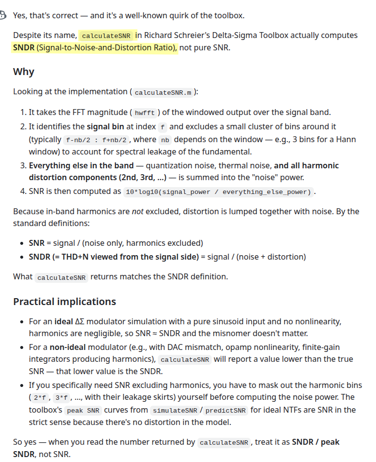
calculateSNR
1 | function snr = calculateSNR(hwfft,f,nsig) |
reference
Pavan, Shanthi, Richard Schreier, and Gabor Temes. (2016). Understanding Delta-Sigma Data Converters. 2nd ed. Wiley.
Norsworthy, Steven R., Richard Schreier, Gábor C. Temes and Ieee Circuits. “Delta-sigma data converters : theory, design, and simulation.” (1997).
Horowitz, P., & Hill, W. (2015). The art of electronics (3rd ed.). Cambridge University Press.
John Rogers, Calvin Plett, and Foster Dai. 2006. Integrated Circuit Design for High-Speed Frequency Synthesis (Artech House Microwave Library). Artech House, Inc., USA.
Razavi B. Analysis and Design of Data Converters. Cambridge University Press; 2025.
R. Schreier, ISSCC2006 tutorial: Understanding Delta-Sigma Data Converters
Shanthi Pavan, ISSCC2013 T5: Simulation Techniques in Data Converter Design [https://www.nishanchettri.com/isscc-slides/2013%20ISSCC/TUTORIALS/ISSCC2013Visuals-T5.pdf]
Bruce A. Wooley , 2012, "The Evolution of Oversampling Analog-to-Digital Converters" [https://r6.ieee.org/scv-sscs/wp-content/uploads/sites/80/2012/06/Oversampling-Wooley_SCV-ver2.pdf]
Venkatesh Srinivasan, ISSCC 2019 T5: Noise Shaping in Data Converters
B. Razavi, "The Delta-Sigma Modulator [A Circuit for All Seasons]," IEEE Solid-State Circuits Magazine, Volume. 8, Issue. 20, pp. 10-15, Spring 2016. [http://www.seas.ucla.edu/brweb/papers/Journals/BRSpring16DeltaSigma.pdf]
P. M. Aziz, H. V. Sorensen and J. vn der Spiegel, "An overview of sigma-delta converters," in IEEE Signal Processing Magazine, vol. 13, no. 1, pp. 61-84, Jan. 1996 [https://sci-hub.st/10.1109/79.482138]
Richard E. Schreier, ECE 1371 Advanced Analog Circuits - 2015 [http://individual.utoronto.ca/schreier/ece1371-2015.html]
Gabor C. Temes. ECE 627-Oversampled Delta-Sigma Data Converters [https://classes.engr.oregonstate.edu/eecs/spring2017/ece627/lecturenotes.html]
Joshua Reiss. Understanding sigma delta modulation: the solved and unsolved issues
V. Medina, P. Rombouts and L. Hernandez-Corporales, "A Different View of Sigma-Delta Modulators Under the Lens of Pulse Frequency Modulation [Feature]," in IEEE Circuits and Systems Magazine, vol. 24, no. 2, pp. 80-97, Secondquarter 2024
Carsten Wulff , Oversampling and Sigma-Delta ADCs [https://analogicus.com/aic2026/oversampling_and_sigma-delta_adcs]