Switched-Capacitor Circuits
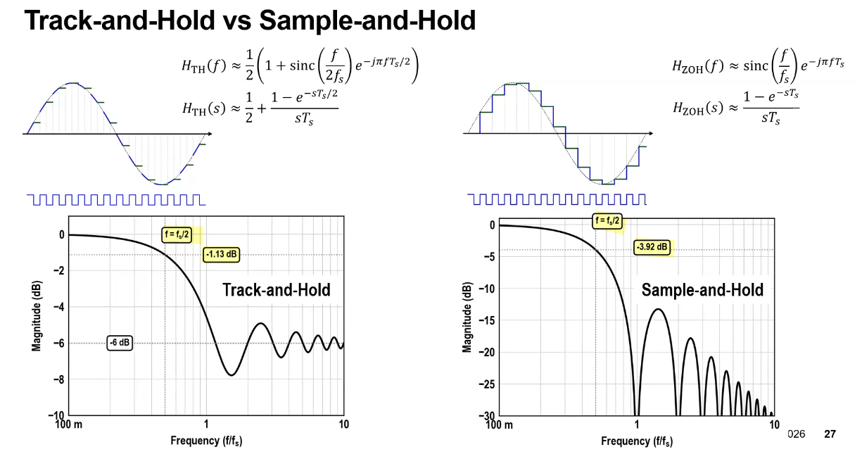
Track-and-Hold (TH)


 \[
H_\mathrm{TH}(f) \approx \frac{1}{2}
\left(
1 + \mathrm{sinc}\left( \frac{f}{2f_s} \right)e^{-j\pi f T_s/2}
\right)
\]
\[
H_\mathrm{TH}(f) \approx \frac{1}{2}
\left(
1 + \mathrm{sinc}\left( \frac{f}{2f_s} \right)e^{-j\pi f T_s/2}
\right)
\]

PSS+PAC SImulaiton [https://youtu.be/VLdcY76V9Ss]

Sample-and-Hold (SH)
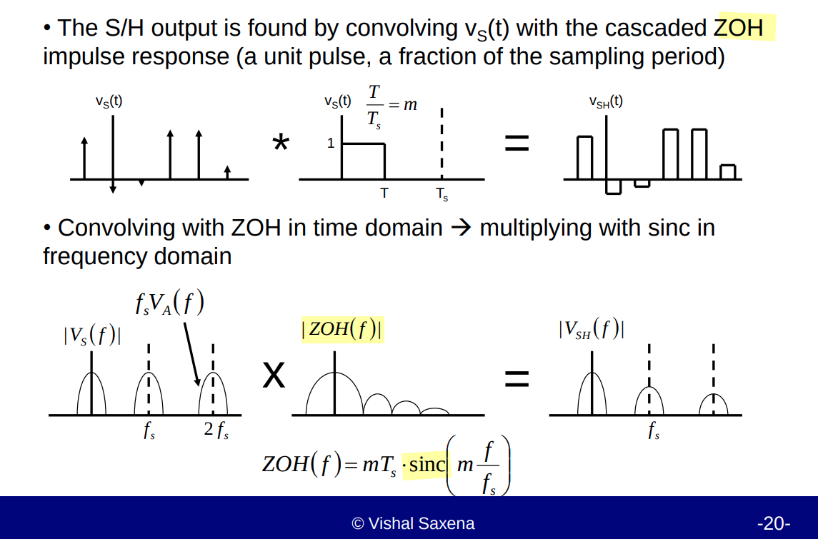
Zero-Order Hold

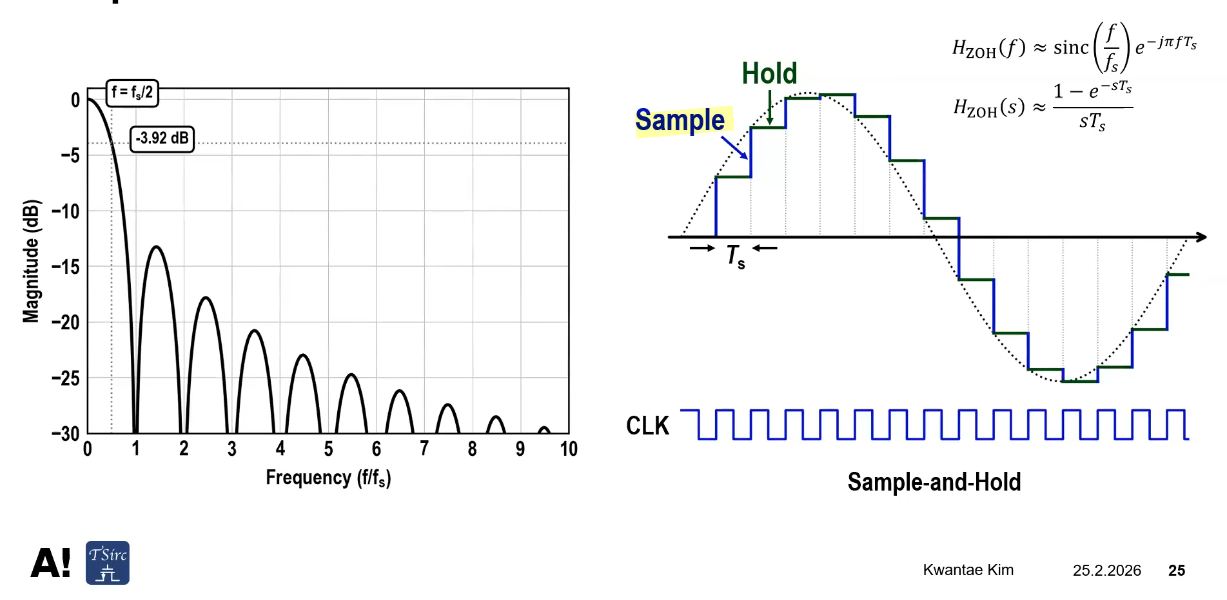
Given \(\color{red}T_p = T_s\) \[ H_\mathrm{SH}(f) \approx \mathrm{sinc}\left( \frac{f}{f_s} \right)e^{-j\pi f T_s} \]
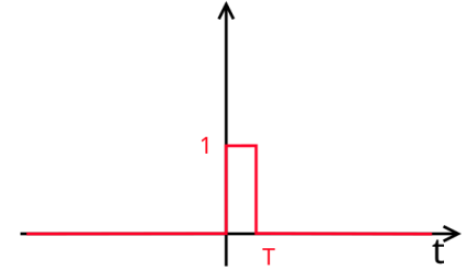 \[
h_{ZOH}(t) = \text{rect}(\frac{t}{T} - \frac{1}{2}) = \left\{
\begin{array}{cl}
1 & : \ 0 \leq t \lt T \\
0 & : \ \text{otherwise}
\end{array} \right.
\] The effective frequency response is the continuous Fourier
transform of the impulse response \[
H_{ZOH}(f) = \mathcal{F}\{h_{ZOH}(t)\} = T\frac{1-e^{j2\pi fT}}{j2\pi
fT}=Te^{-j\pi fT}\text{sinc}(fT)
\] where \(\text{sinc}(x)\) is
the normalized sinc function \(\frac{\sin(\pi
x)}{\pi x}\)
\[
h_{ZOH}(t) = \text{rect}(\frac{t}{T} - \frac{1}{2}) = \left\{
\begin{array}{cl}
1 & : \ 0 \leq t \lt T \\
0 & : \ \text{otherwise}
\end{array} \right.
\] The effective frequency response is the continuous Fourier
transform of the impulse response \[
H_{ZOH}(f) = \mathcal{F}\{h_{ZOH}(t)\} = T\frac{1-e^{j2\pi fT}}{j2\pi
fT}=Te^{-j\pi fT}\text{sinc}(fT)
\] where \(\text{sinc}(x)\) is
the normalized sinc function \(\frac{\sin(\pi
x)}{\pi x}\)
The Laplace transform transfer function of the ZOH is found by substituting \(s=j2\pi f\) \[ H_{ZOH}(s) = \mathcal{L}\{h_{ZOH}(t)\}=\frac{1-e^{-sT}}{s} \]
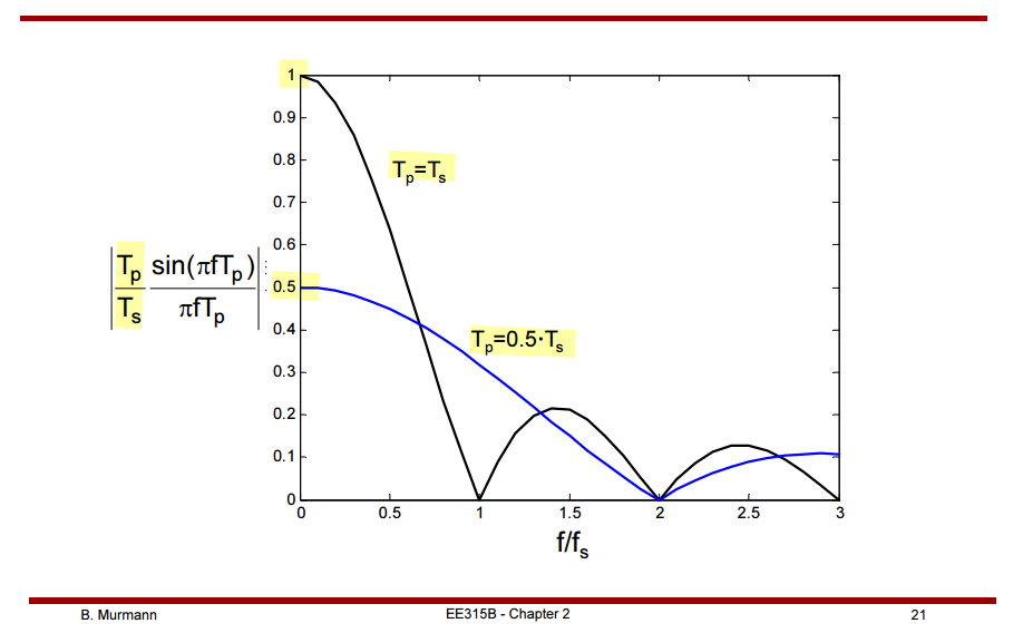
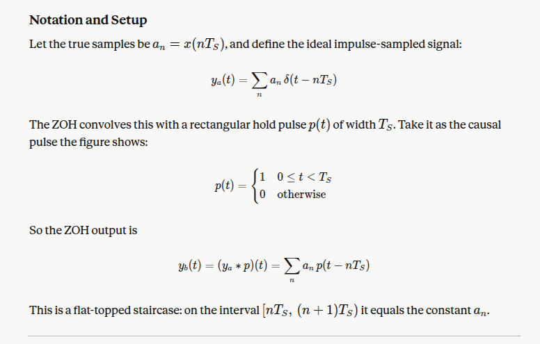
Sinc Droop of ZOH sampler
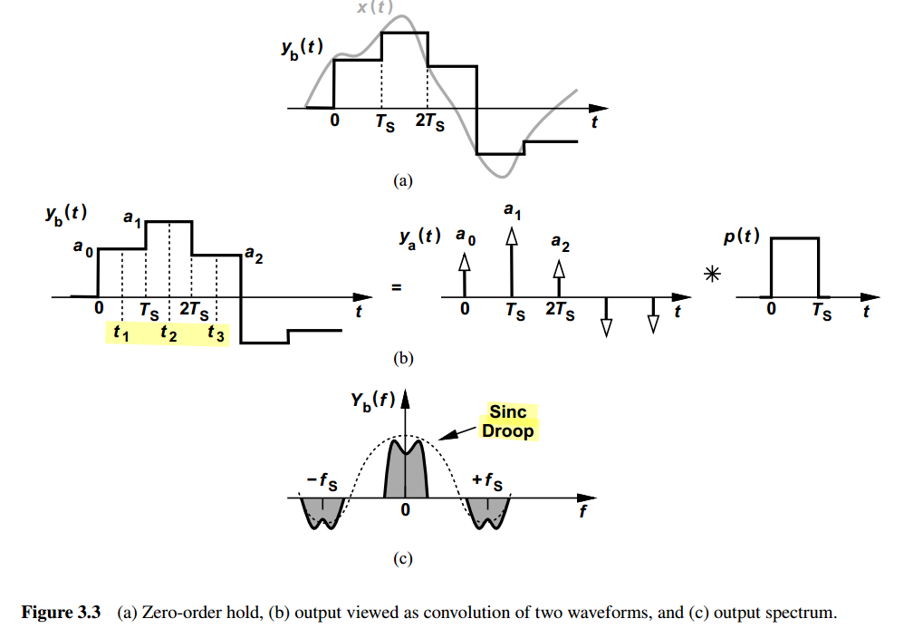
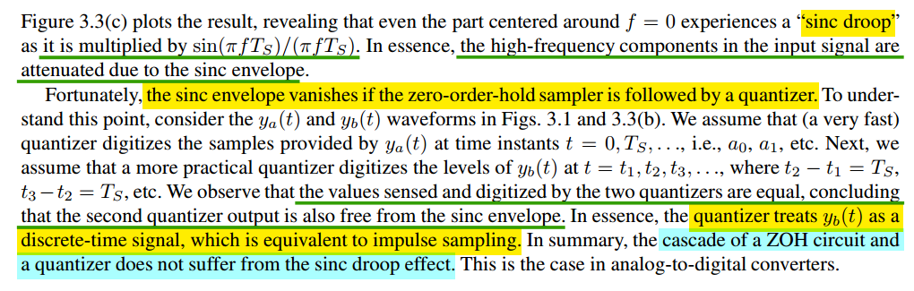
Time-Domain Argument
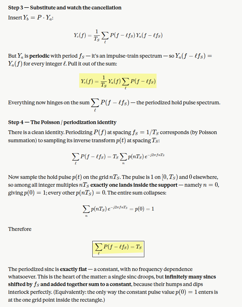
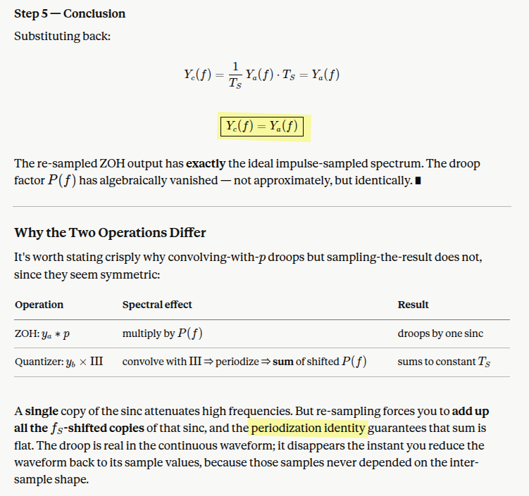
Frequency-Domain Argument
Switched-Capacitor Filter
Kwantae Kim, Integrated Analog Systems D - Lecture 08 (Switched-Capacitor Filter) [https://youtu.be/G0lzrMll-Ho]
—, Integrated Analog Systems D - Lecture 10 CAD (Switched-Capacitor Filter) [[https://youtu.be/eMOFMjuKiJQ]
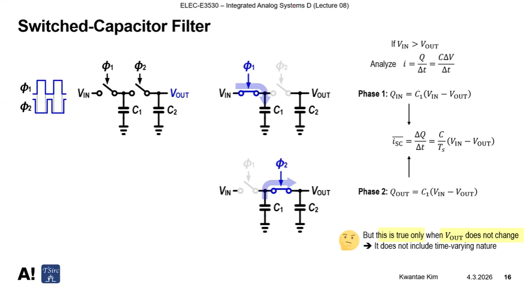
switched-Capacitor Resistor
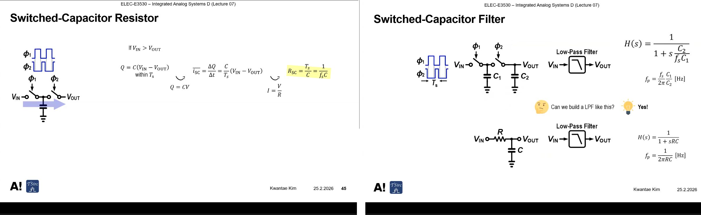
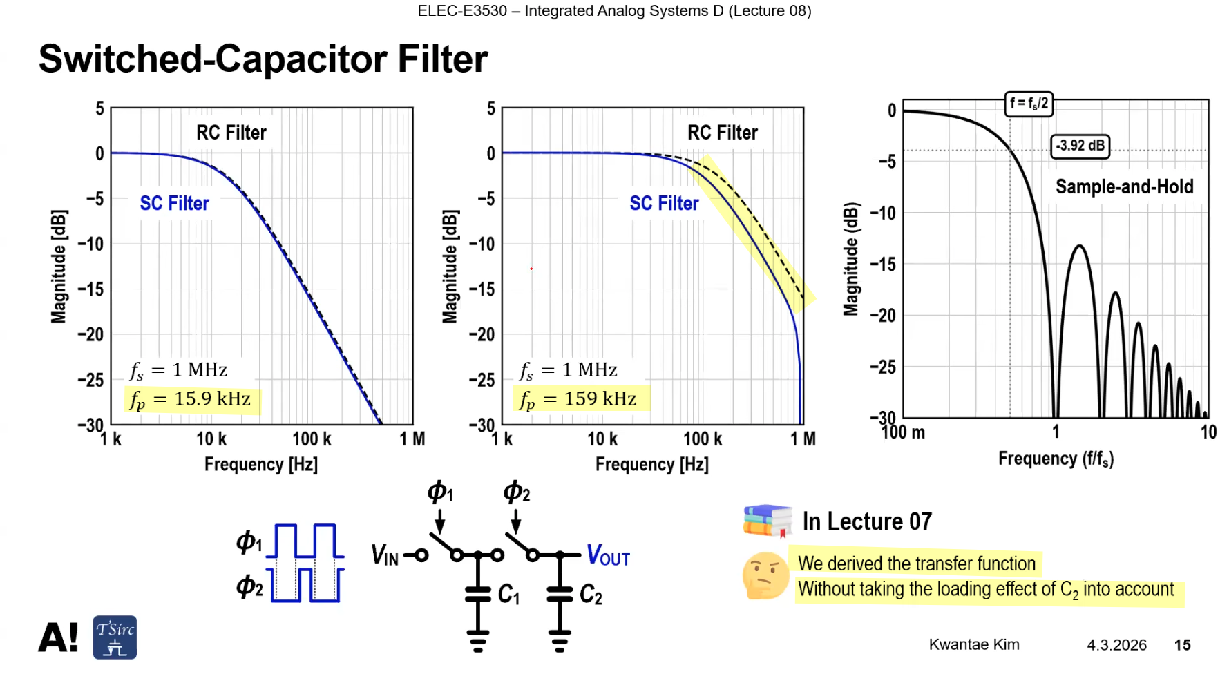
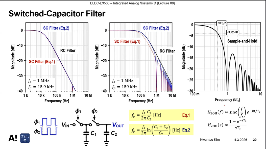
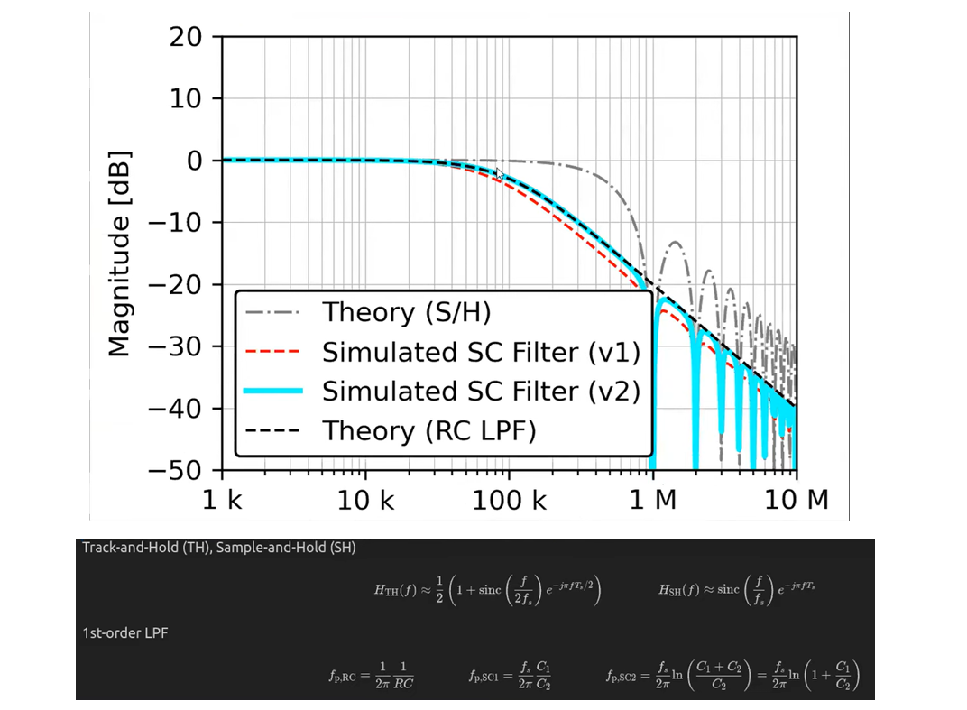
Due to not taking loading \(C_2\) into account, actual switched-capacitor filter deviate from equivalent \(R_{SC}\) + \(C_2\) low pass filter as \(f_p\) approaching to \(f_s\)
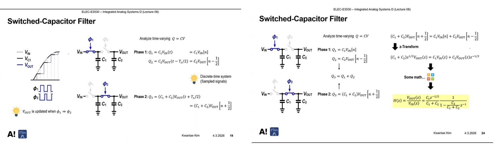 \[
\color{red}H(z)
=\frac{V_{OUT}(z)}{V_{IN}(z)}=\frac{C_1z^{-1/2}}{C_1+C_2}\frac{1}{1-\frac{C_2}{C_1+C_2}z^{-1}}
\]
\[
\color{red}H(z)
=\frac{V_{OUT}(z)}{V_{IN}(z)}=\frac{C_1z^{-1/2}}{C_1+C_2}\frac{1}{1-\frac{C_2}{C_1+C_2}z^{-1}}
\]
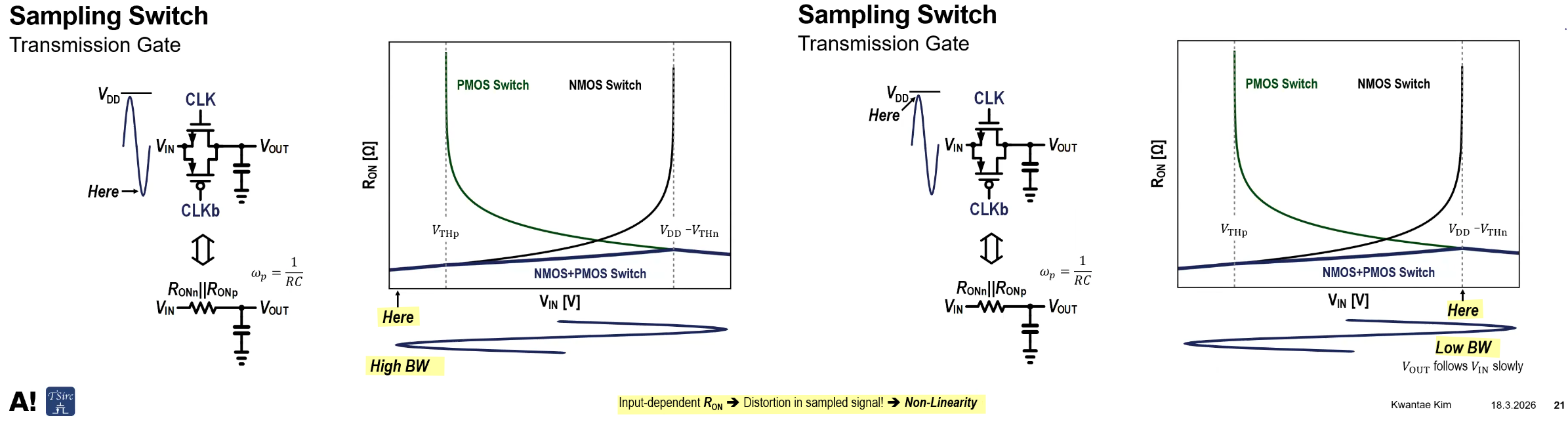
Sampling Switch
Kwantae Kim, Integrated Analog Systems D - Lecture 10 (ADC) [https://youtu.be/IEdbLNJb9wQ]
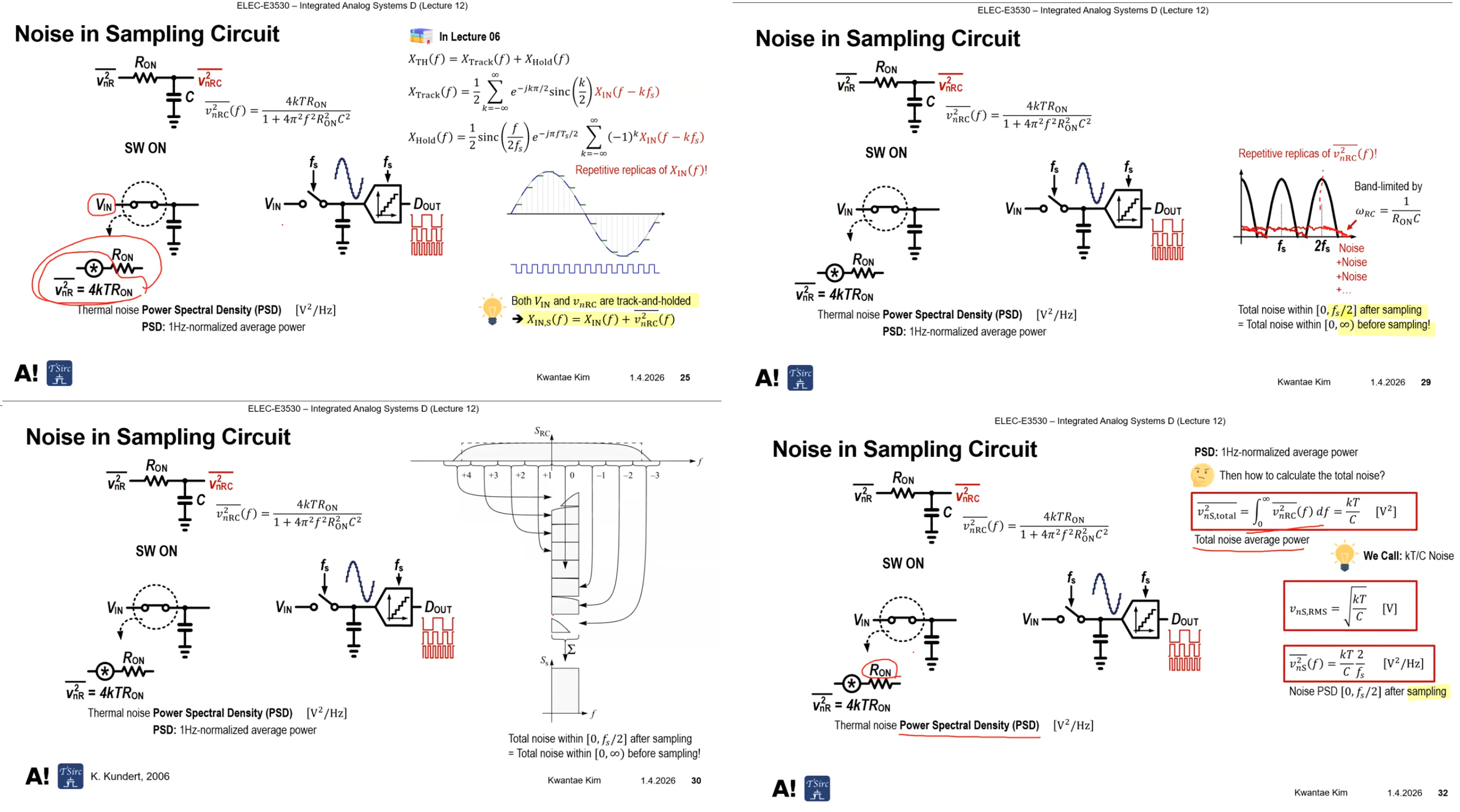
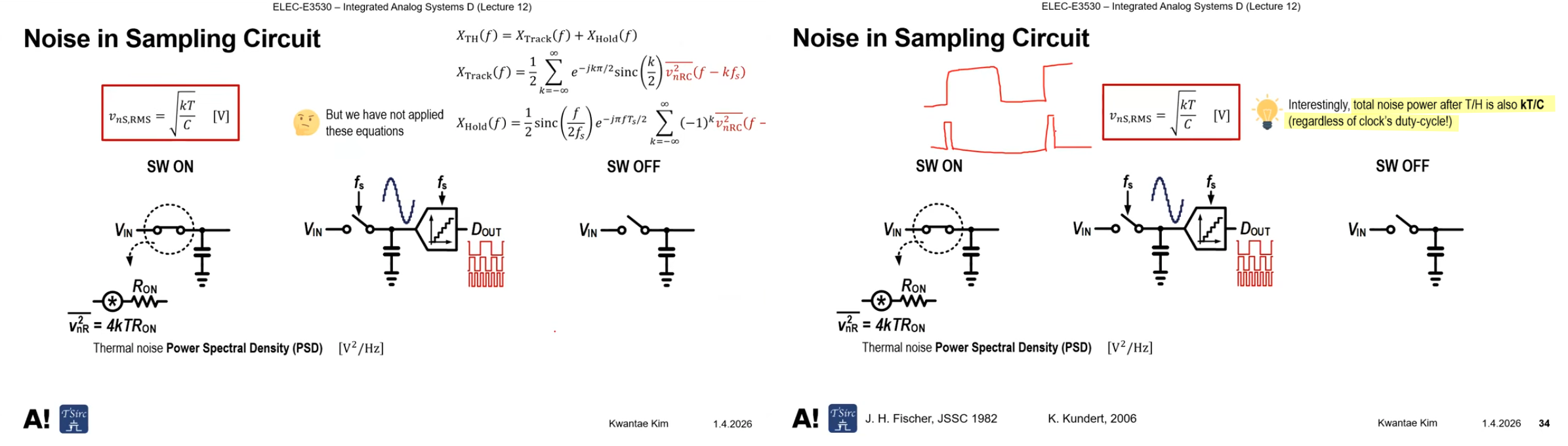
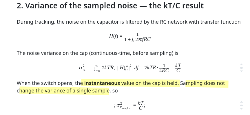
Noise In Sampling Circuit
Kwantae Kim, Integrated Analog Systems D - Lecture 12 (ADC) [https://youtu.be/NkSitVkPNig]
Shanthi Pavan , 6.4 - kT/C noise in a sample-and-hold circuit [https://youtu.be/EmyMuRswsjo]
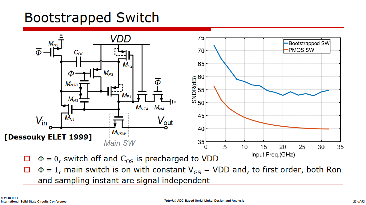
Bootstrapped Switch
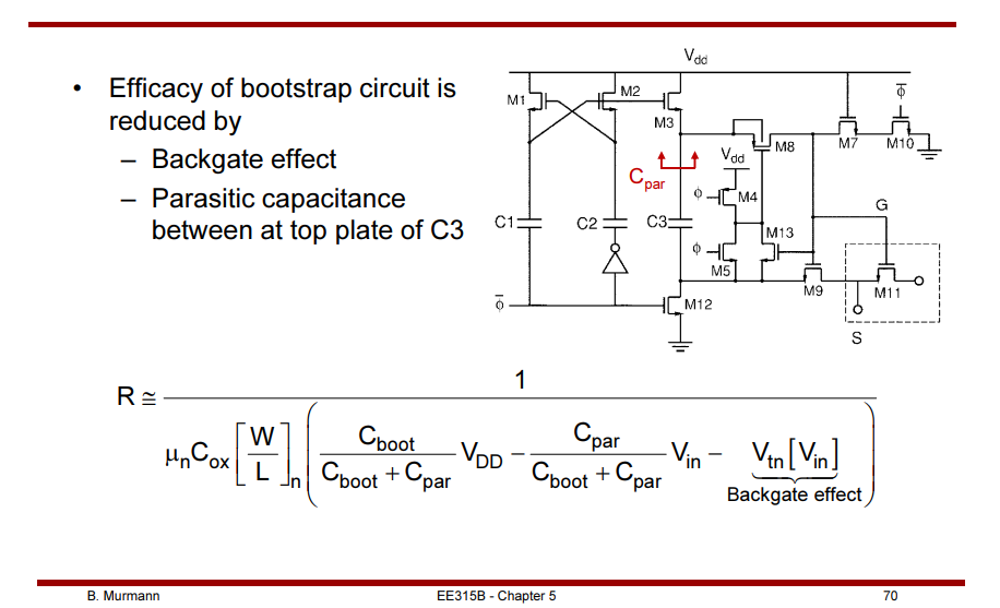
A. Abo et al., "A 1.5-V, 10-bit, 14.3-MS/s CMOS Pipeline Analog-to Digital Converter," IEEE J. Solid-State Circuits, pp. 599, May 1999 [https://sci-hub.se/10.1109/4.760369]
Dessouky and Kaiser, "Input switch configuration suitable for rail-to-rail operation of switched opamp circuits," Electronics Letters, Jan. 1999. [https://sci-hub.se/10.1049/EL:19990028]
B. Razavi, "The Bootstrapped Switch [A Circuit for All Seasons]," in IEEE Solid-State Circuits Magazine, vol. 7, no. 3, pp. 12-15, Summer 2015 [https://www.seas.ucla.edu/brweb/papers/Journals/BRSummer15Switch.pdf]
B. Razavi, "The Design of a bootstrapped Sampling Circuit [The Analog Mind]," IEEE Solid-State Circuits Magazine, Volume. 13, Issue. 1, pp. 7-12, Summer 2021. [http://www.seas.ucla.edu/brweb/papers/Journals/BR_SSCM_1_2021.pdf]
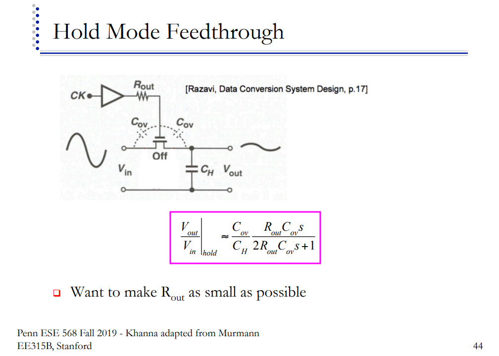
Hold Mode Feedthrough
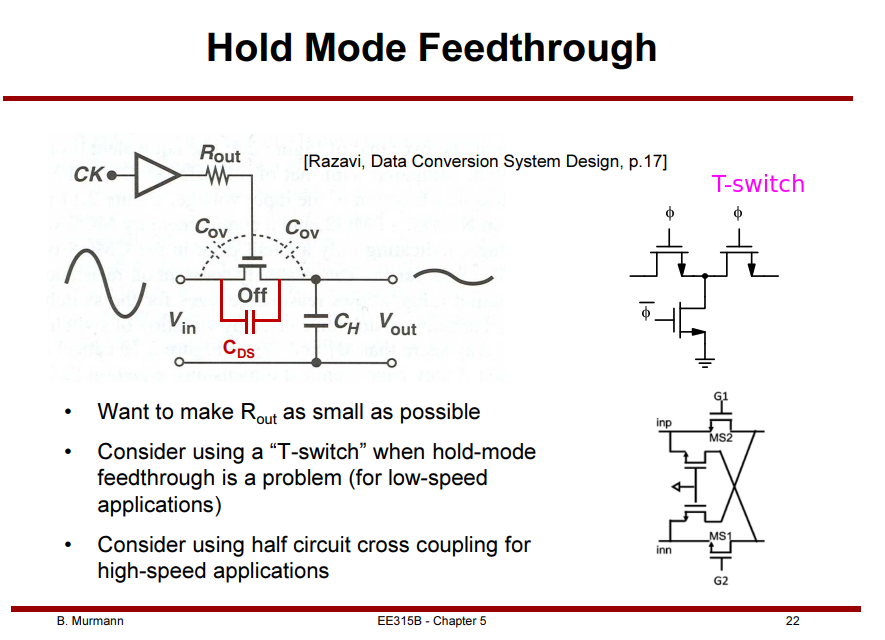
P. Schvan et al., "A 24GS/s 6b ADC in 90nm CMOS," 2008 IEEE International Solid-State Circuits Conference - Digest of Technical Papers, San Francisco, CA, USA, 2008, pp. 544-634
B. Sedighi, A. T. Huynh and E. Skafidas, "A CMOS track-and-hold circuit with beyond 30 GHz input bandwidth," 2012 19th IEEE International Conference on Electronics, Circuits, and Systems (ICECS 2012), Seville, Spain, 2012, pp. 113-116
Tania Khanna, ESE 568: Mixed Signal Circuit Design and Modeling [https://www.seas.upenn.edu/~ese5680/fall2019/handouts/lec11.pdf]
Clock Feedthrough
aka. LO leakage
TODO 📅
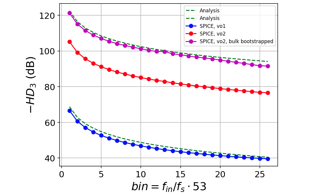
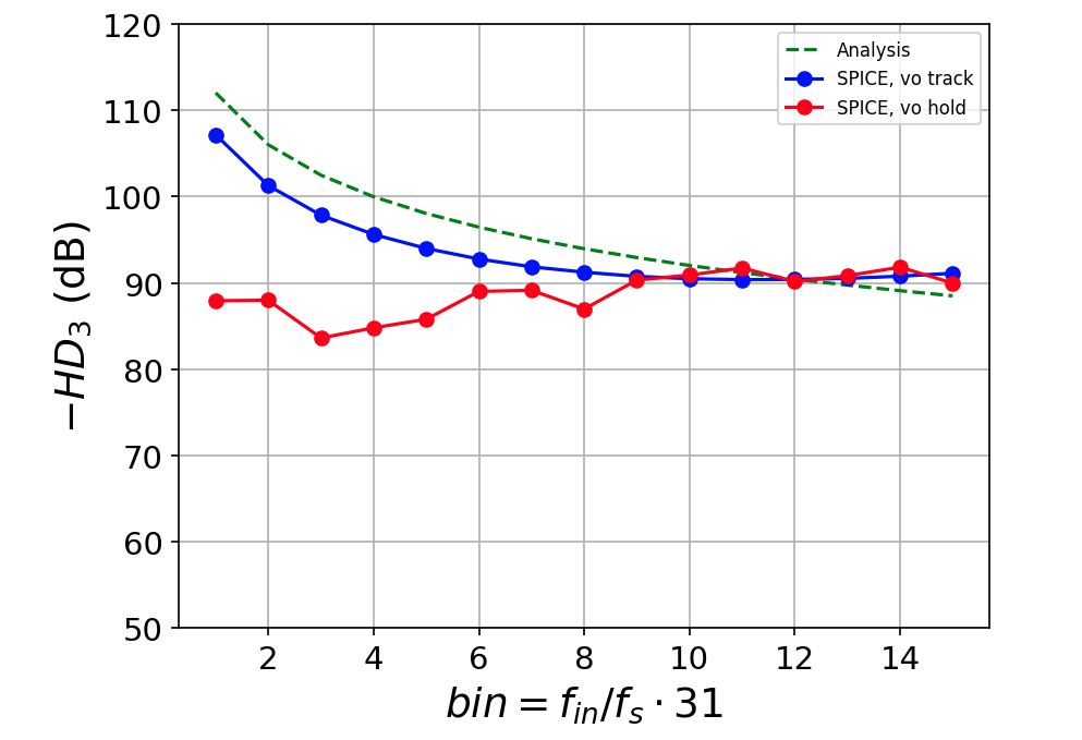
analytical expression for \(HD_3\)
Boris Murmann, MEAD2026 [https://github.com/bmurmann/MEAD2026]
HW #1 - “ICONS 2026: Masterclass Series on Advanced IC Design” Online Course - May 2026 [https://youtu.be/hS2ZY_UHh_0]
In most differential designs, \(HD_3\) is of primary concern, where even harmonics are absent
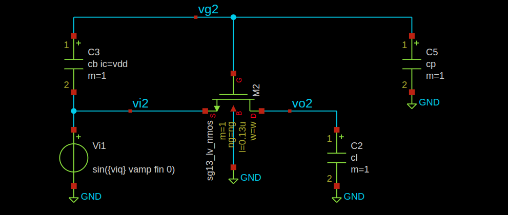
Plain NMOS switch
[https://github.com/bmurmann/MEAD2026/blob/main/xschem/tb_track_nmos.sch]
1 | .param vdd=1.2 viq=0.3 vamp=0.2 |
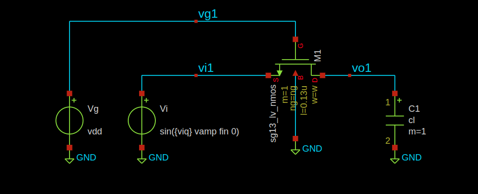
sinusoidal source waveform, using parameters:
DC offset = viq,amplitude = vamp,frequency = fin,delay = 0Vth is about 0.466, then
vov=vdd-vth-viq = 1.2-0.466-0.3=0.434
1 | ## https://github.com/bmurmann/MEAD2026/blob/main/tb_track_nmos.ipynb |
\[ \color{red}HD_3 \approx \frac{1}{2} \cdot \frac{f_{in}}{f_{BW}} \cdot \left(\frac{V_m}{V_{OV}}\right)^2 \]
Pure Ron-modulation distortion. No bootstrap
term, no body-effect term
Bootstrapped switch — ideal
[https://github.com/bmurmann/MEAD2026/blob/main/xschem/tb_track_nmos.sch]
1 | .param vdd=1.2 viq=0.3 vamp=0.2 |
Vth is about 0.466, then
vov=vdd-vth = 1.2-0.466=0.734
1 | ## https://github.com/bmurmann/MEAD2026/blob/main/tb_track_nmos.ipynb |
\[ \color{red}HD_3 \approx \frac{1}{2} \cdot \frac{f_{in}}{f_{BW}} \cdot \left(\frac{V_m}{V_{OV}}\right)^2 \cdot \left(\frac{C_p}{C_B}\right)^2 \]
Adds the bootstrap parasitic-ratio term. No body-effect floor
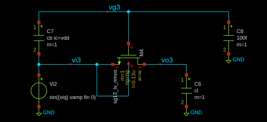
Bootstrapped switch — with body effect
[https://github.com/bmurmann/MEAD2026/blob/main/xschem/tb_boot.sch]
1 | .param vdd=1.2 viq=0.3 vamp=0.2 |
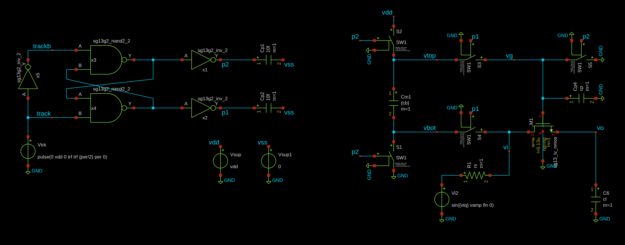
ss: small signal; ls: large signal;
1.6e-15: capacitance per M1 MOS (Main Switch) width
1 | ## https://github.com/bmurmann/MEAD2026/blob/main/tb_boot.ipynb |
\[ \color{red}HD_3 \approx \frac{1}{2} \cdot \frac{f_{in}}{f_{BW}} \cdot \left(\frac{V_m}{V_{OV}}\right)^2 \cdot \left(\frac{C_{p,ss}}{C_B} + 0.11\right)^2 \]
The +0.11 is the residual Vt(vin)
body-effect contribution that the bootstrap cannot cancel.
[https://github.com/bmurmann/MEAD2026/blob/main/tb_boot_bottom_4.ipynb]
1 | ### fin, fin +/-N*fs |
Integrator
TODO 📅
[https://www.eecg.utoronto.ca/~johns/ece1371/slides/10_switched_capacitor.pdf]
[https://www.seas.ucla.edu/brweb/papers/Journals/BRWinter17SwCap.pdf]
[https://class.ece.iastate.edu/ee508/lectures/EE%20508%20Lect%2029%20Fall%202016.pdf]
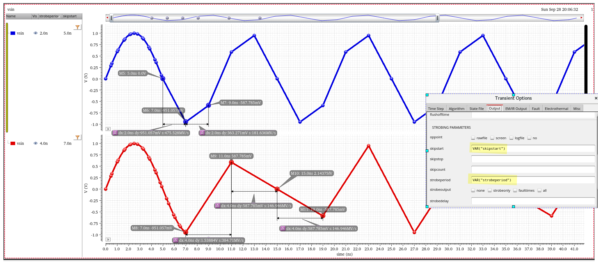
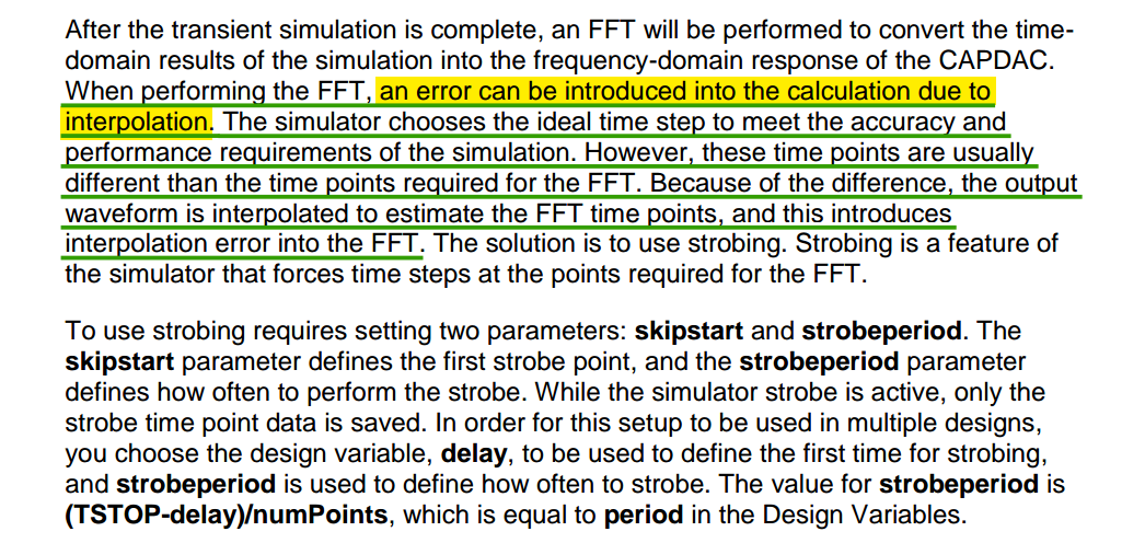
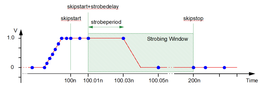
simulation setup
strobeperiod
ADC Verification Rapid Adoption Kit (RAK)
Spectre Tech Tips: Using the Spectre Strobe Feature [https://community.cadence.com/cadence_blogs_8/b/cic/posts/spectre-tech-tips-using-the-spectre-strobe-feature]
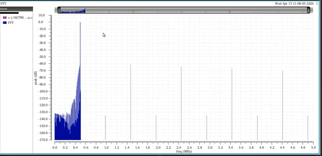
FFT in Cadence [https://www.rfinsights.com/cadence/fft-in-cadence/]
PSS spectrum vs. FFT
Kwantae Kim, Integrated Analog Systems D - Lecture 14S CAD (Linearity and FFT) [https://youtu.be/qwJ_tlZTaq8]
FFT analysis need sampling, then aliasing occur
Bootstrapped Switch
Kwantae Kim, Integrated Analog Systems D - Lecture 14S CAD (Linearity and FFT) [https://youtu.be/qwJ_tlZTaq8]
Sampled PAC (Spectre RF) Analysis - Strange results ? [https://designers-guide.org/forum/YaBB.pl?num=1590925194]
Vishal Saxena, "SpectreRF Periodic Analysis" [https://www.eecis.udel.edu/~vsaxena/courses/ece614/Handouts/SpectreRF%20Periodic%20Analysis.pdf]
[https://designers-guide.org/forum/YaBB.pl?num=1590925194/1#1]
PSS + SampledPAC should be suitable to characterize bootstrapped switch
It's the hold function that is responsible for the \(\operatorname{sinc}()\) behavior
reference
Boris Murmann. EE315A VLSI Signal Conditioning Circuits [pdf]
Kwantae Kim. ELEC-E3530 Integrated Analog Systems D (5 ECTS) [video] [github]
R. S. Ashwin Kumar, Analog circuits for signal processing [https://home.iitk.ac.in/~ashwinrs/2022_EE698W.html]
R. Gregorian and G. C. Temes. Analog MOS Integrated Circuits for Signal Processing. Wiley-Interscience, 1986 [pdf]
Christian-Charles Enz. "High precision CMOS micropower amplifiers" [pdf]
Negar Reiskarimian. CICC 2025 Insight: Switched Capacitor Circuits [https://youtu.be/SL3-9ZMwdJQ] [dropbox]
Carsten Wulff, Switched-Capacitor Circuits [https://analogicus.com/aic2026/switched-capacitor_circuits]
rfinsights, switched capacitor analysis [https://www.rfinsights.com/concepts/switched-capacitor-analysis/], [https://www.rfinsights.com/concepts/switched-capacitor-analysis-with-switch-resistance/]