Charge Pump PLL
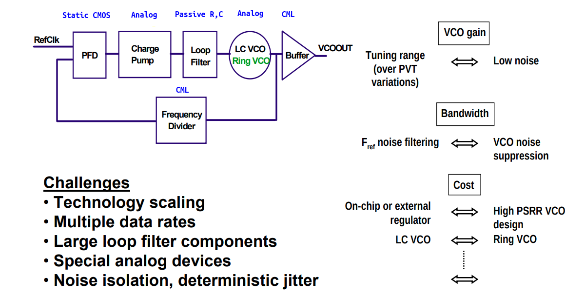
Mehmet Soyuer. Monolithic Phase-Locked Loops for Clocking [https://ewh.ieee.org/r5/denver/sscs/Presentations/2009_06_Soyuer.pdf]
PD & PFD
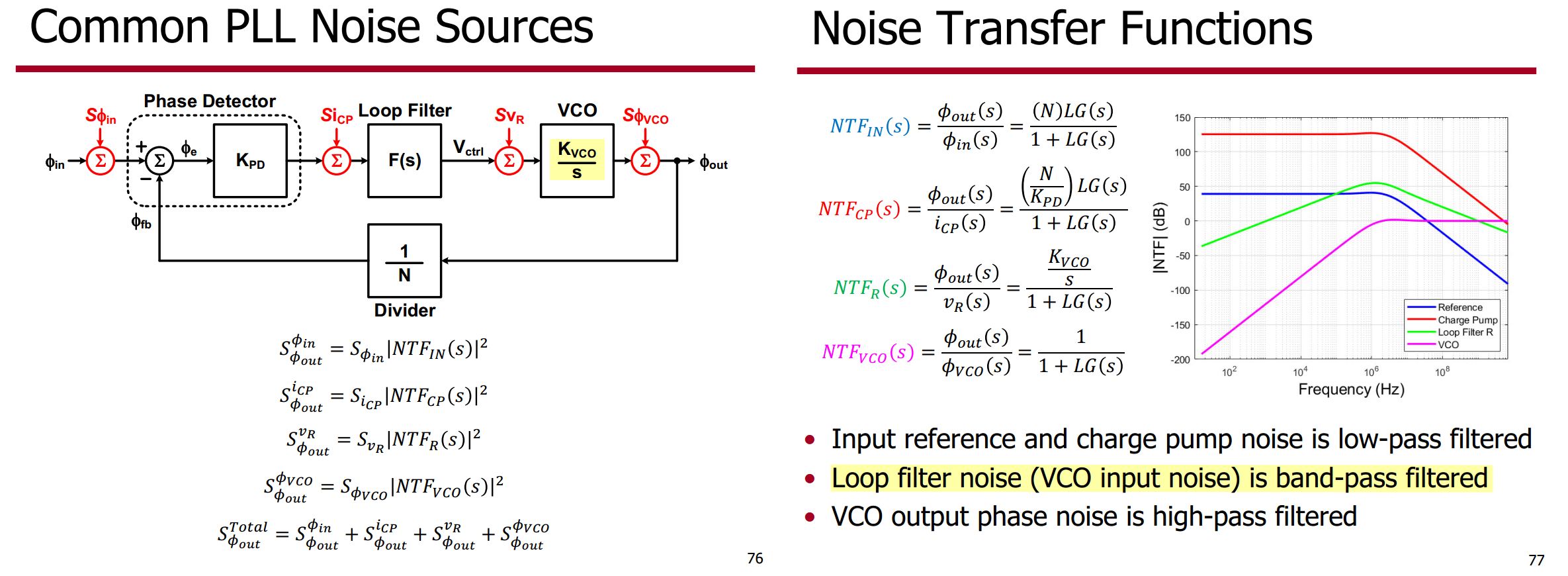
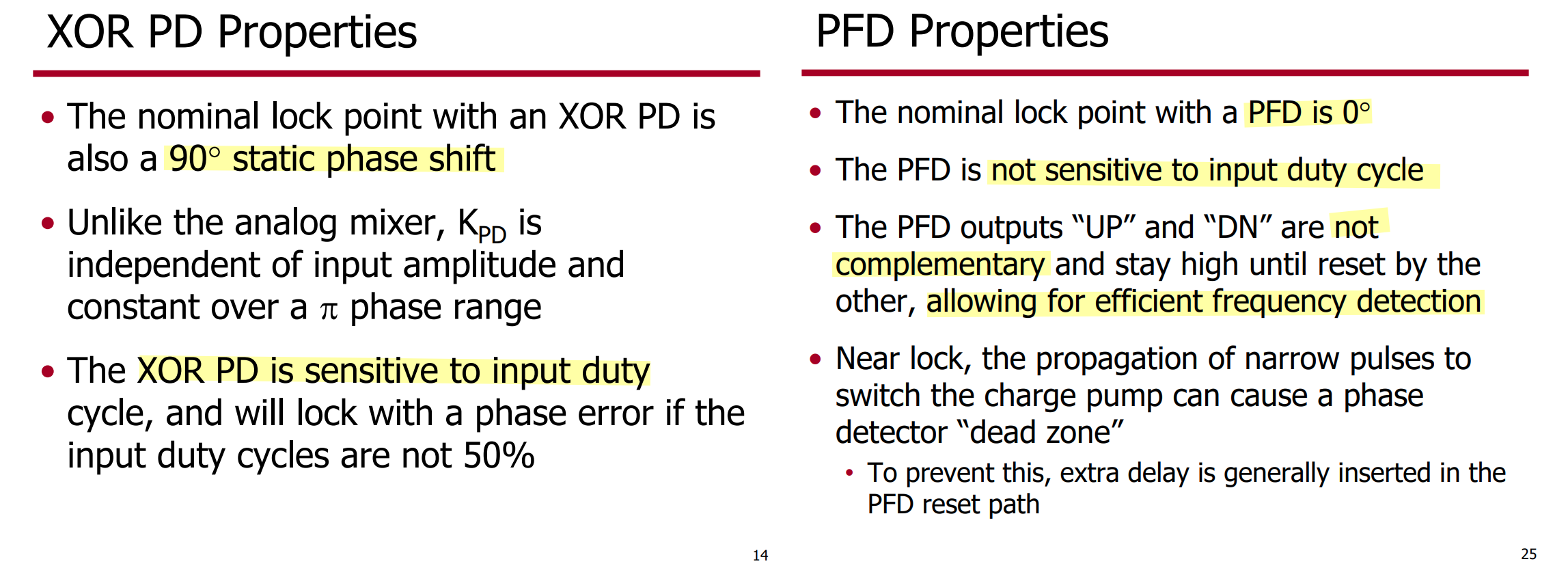
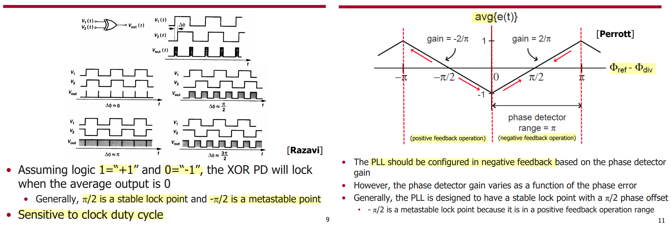
Sam Palermo, ECEN620: Network Theory Broadband Circuit Design Fall 2025 Lecture 4: Phase Detector Circuits [https://people.engr.tamu.edu/spalermo/ecen620/lecture04_ee620_phase_detectors.pdf]
Michael Perrott, 6.976 High Speed Communication Circuits and Systems Lecture 15 Integer-N Frequency Synthesizers [https://rfic.eecs.berkeley.edu/courses/ee242/pdf/perrott_lec15.pdf]
Mehmet Soyuer. Monolithic Phase-Locked Loops for Clocking [https://ewh.ieee.org/r5/denver/sscs/Presentations/2009_06_Soyuer.pdf]
Qasim Chaudhari. What are Cycle Slips and Hangup in Phase Locked Loops? [https://wirelesspi.com/what-are-cycle-slips-and-hangup-in-phase-locked-loops/]
XOR Phase Detector
Tristate PFD
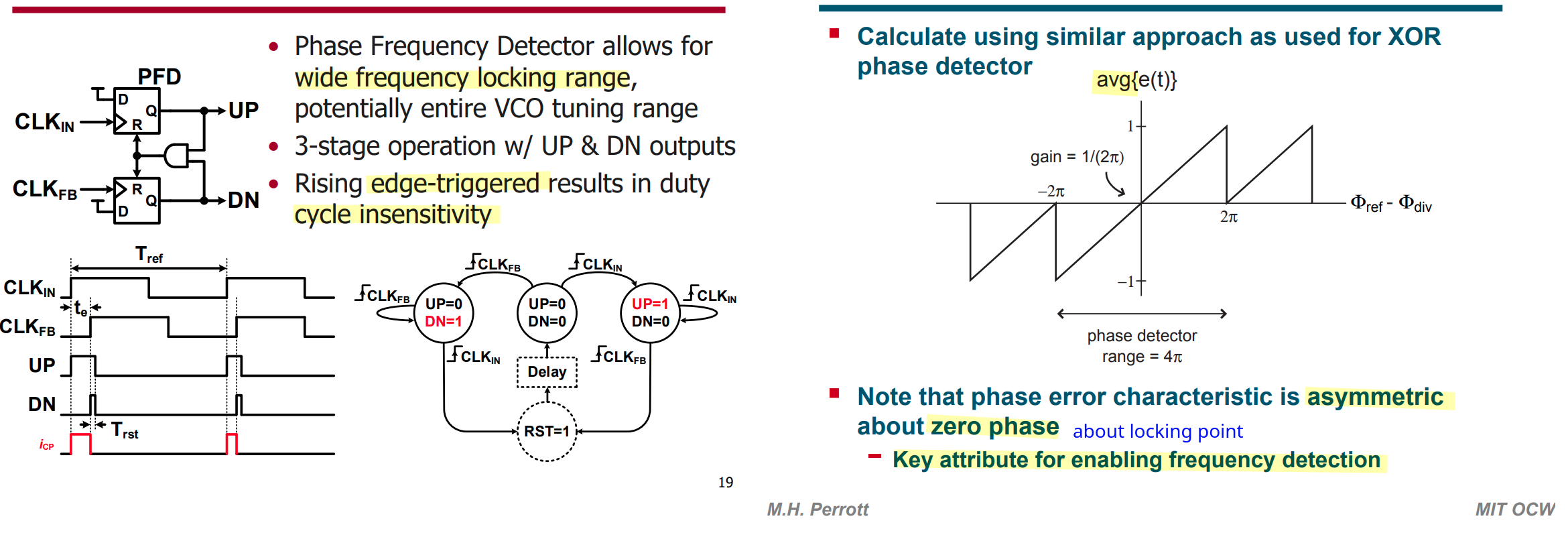
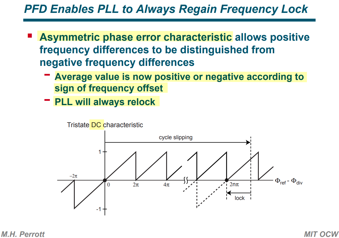
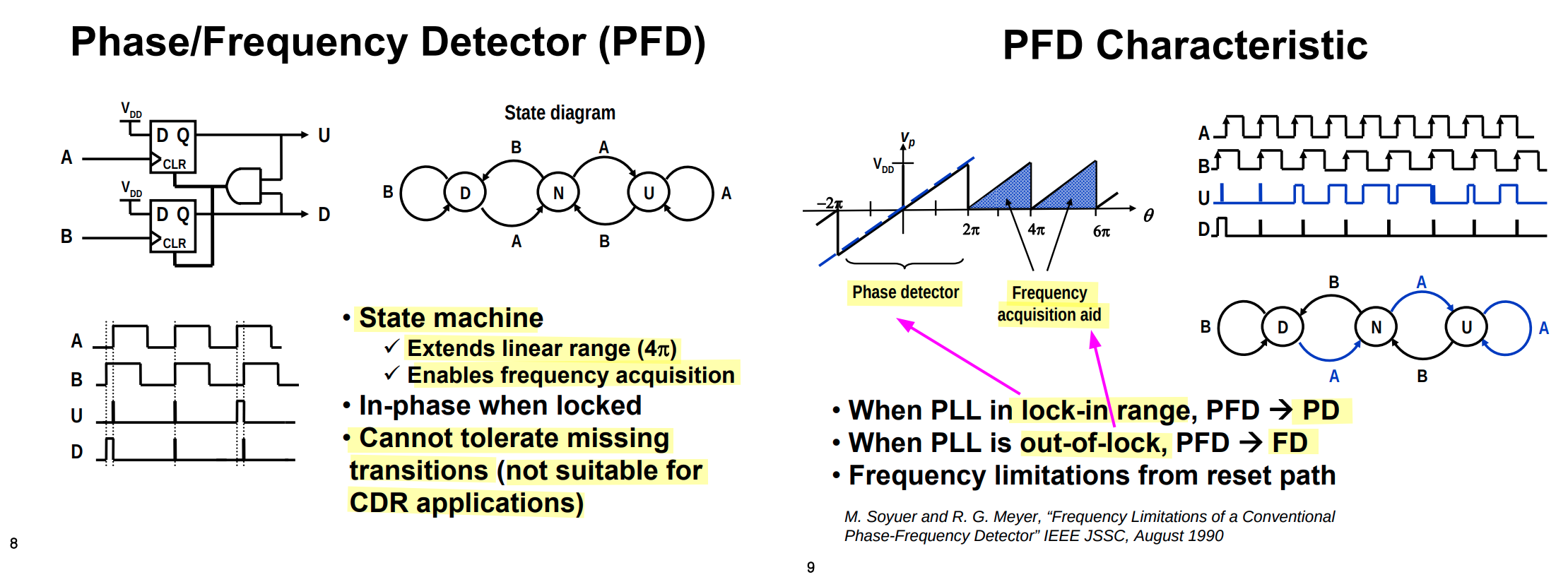
PFD requires periodic edges on both inputs
In a CDR, one input is random NRZ data, and a long run of identical bits has no transitions at all
The PFD's state machine interprets those missing edges as a huge phase/frequency error and pumps the loop away from lock
frequency acquisition
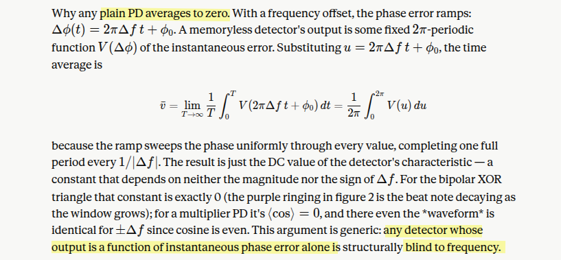
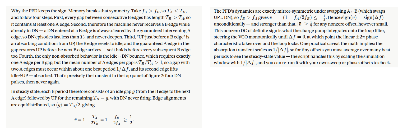
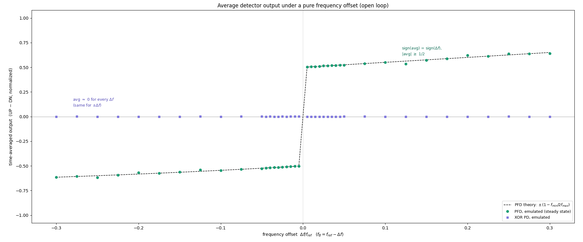
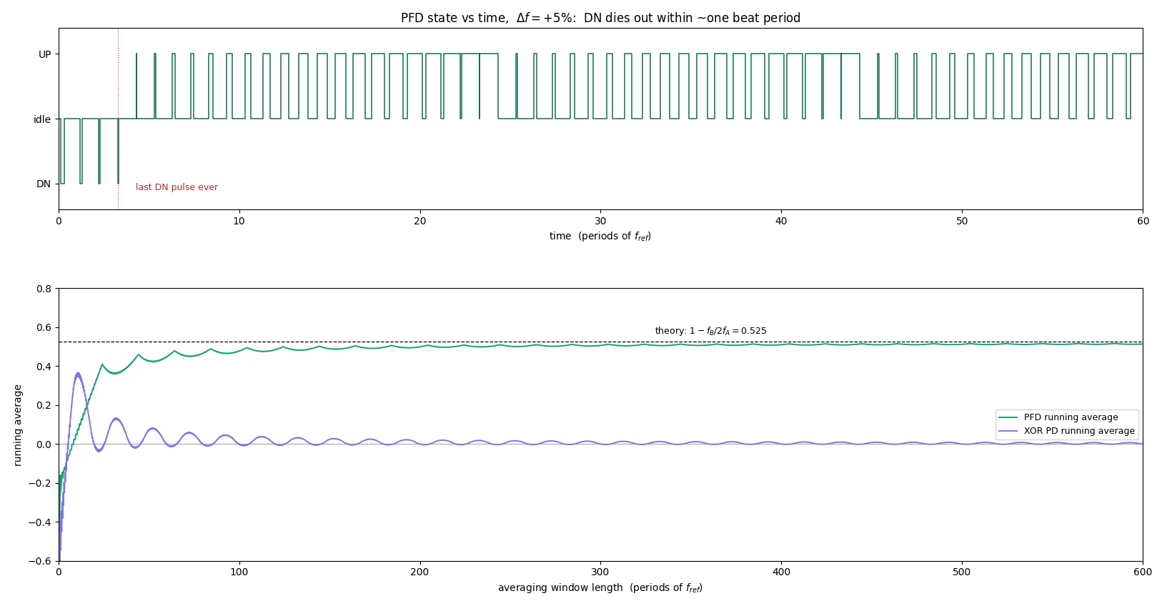
beat period: \(2\pi\cdot T_{beat,per}\cdot \Delta f = 2\pi \to T_{beat,per}=\frac{1}{\Delta f}\)
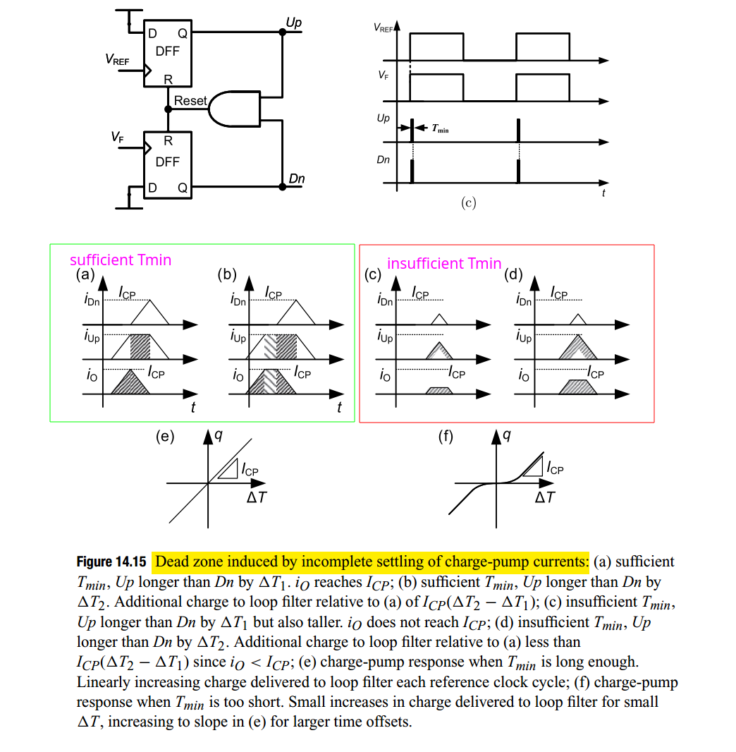
PFD Deadzone
Sam Palermo, "Lecture 4: Phase Detector Circuit" [https://people.engr.tamu.edu/spalermo/ecen620/lecture04_ee620_phase_detectors.pdf]
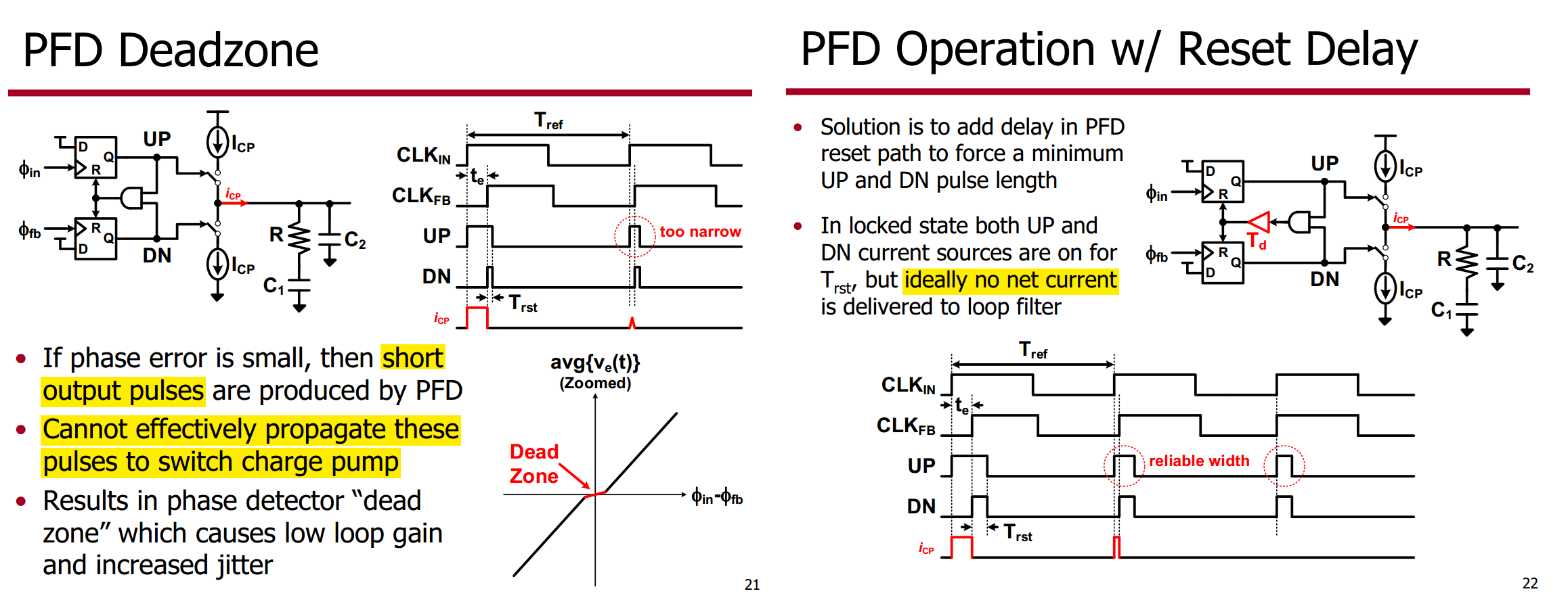
Dead zone induced by incomplete settling of charge-pump currents
This situation can be avoided by adding additional delay to the AND gate in the PFD
D. Turker et al., "A 7.4-to-14GHz PLL with 54fsrms jitter in 16nm FinFET for integrated RF-data-converter SoCs," 2018 IEEE International Solid-State Circuits Conference - (ISSCC), San Francisco, CA, USA, 2018 [[https://sci-hub.ru/10.1109/ISSCC.2018.8310342](
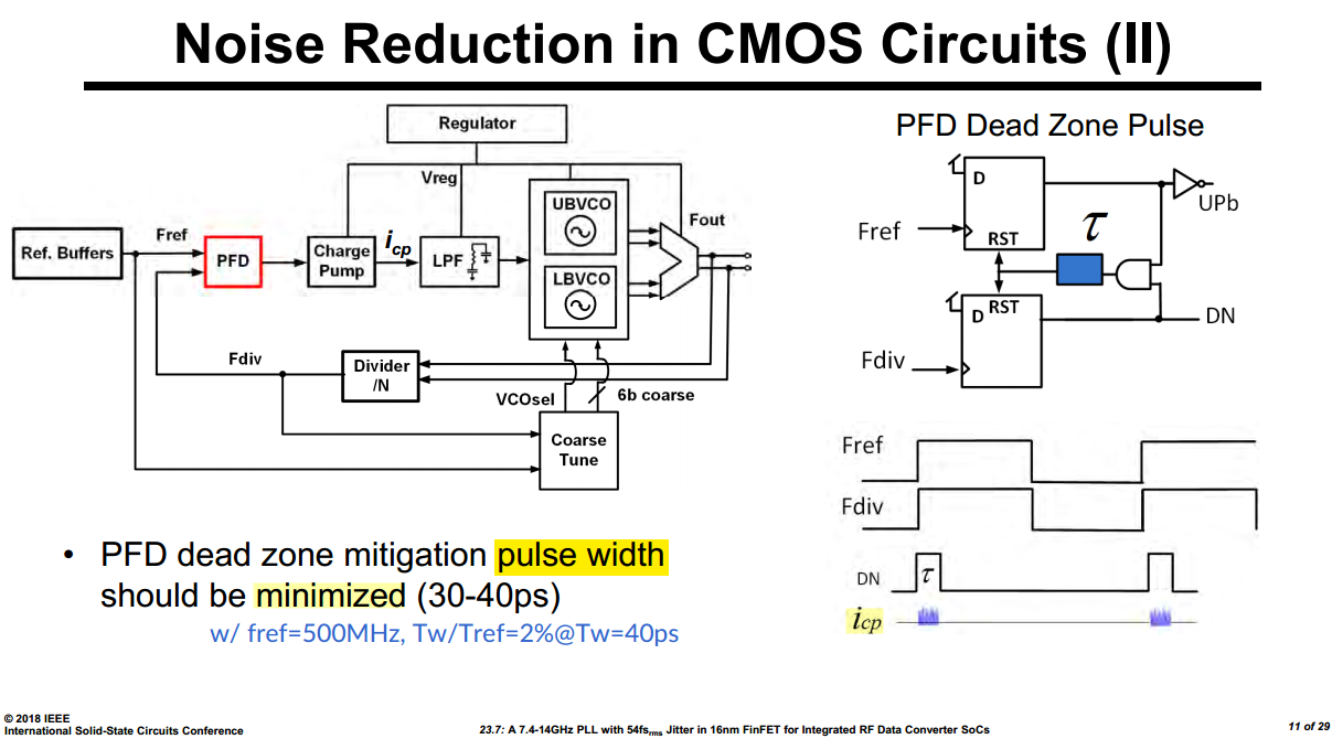
\(\tau\) shall be minimized to reduce noise of CP
PFD/CP Modeling
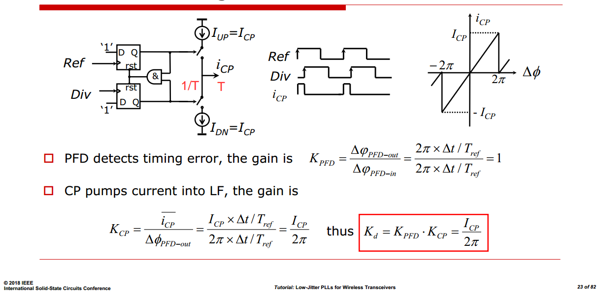

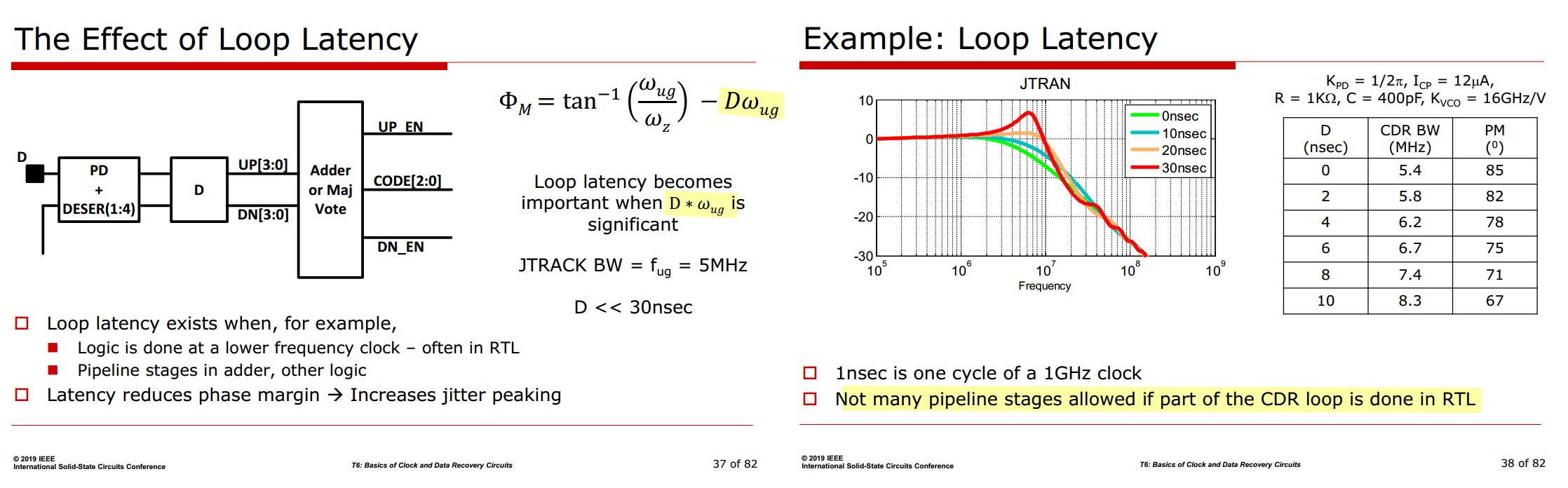
feedback path delay
Dennis Fischette, First Time, Every Time – Practical Tips for PhaseLocked Loop Design [https://www.delroy.com/PLL_dir/tutorial/PLL_tutorial_slides.pdf]
Amir Amirkhany. ISSCC 2019 "Basics of Clock and Data Recovery Circuits"
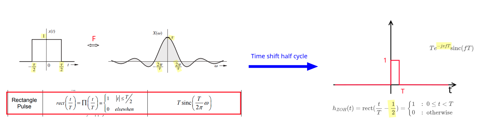
PFD ZOH
PFD ZOH half reference cycle delay in Open-Loop PLL Gain
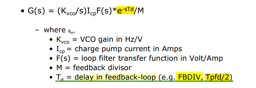
\(\color{red}T_\text{pfd}/2\) term is typically an equivalent delay caused by the sampled-data nature of the PFD/charge-pump
Divider delay
An ideal feedback divider does not introduce propagation delay in phase domain
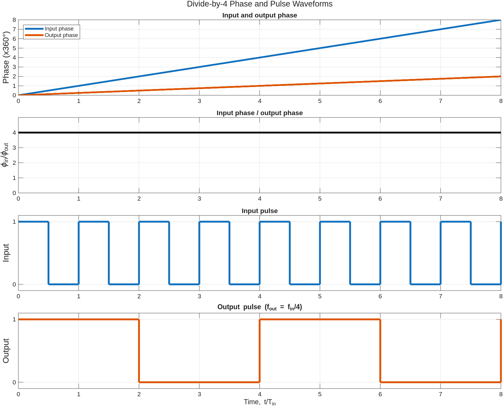
The feedback divider provides a sampled version of the scaled VCO phase, and the PFD obtains the sampled phase error between that feedback phase and the reference phase
There is no delay between oscillator output phase and feedback divider output phase if C2Q and logic propagation delays are neglected
If the real divider has C2Q delay \(t_{CQ}\), then it becomes approximately \[ \boxed{T_d \approx t_{\mathrm{CQ}} + \frac{T_{\mathrm{pfd}}}{2}} \]
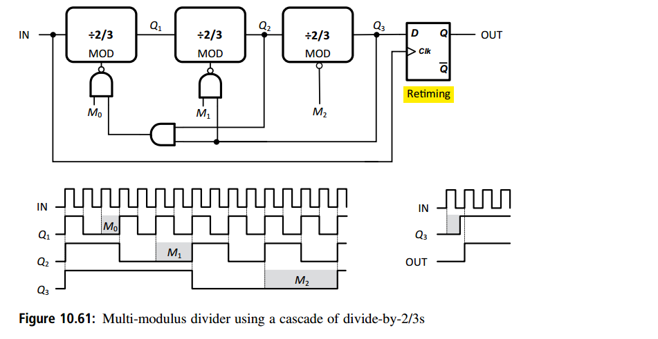
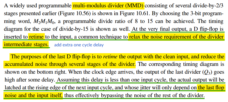
retimer at divider output
Darabi H. Radio Frequency Integrated Circuits and Systems. 2nd ed. Cambridge University Press; 2020.
extra one cycle delay vs reducing accumulated noise from the last DFF retiming DFF
Sam Palermo, ECEN620: Network Theory Broadband Circuit Design Fall 2025 Lecture 8: Divider Circuits [https://people.engr.tamu.edu/spalermo/ecen620/lecture08_ee620_dividers.pdf]
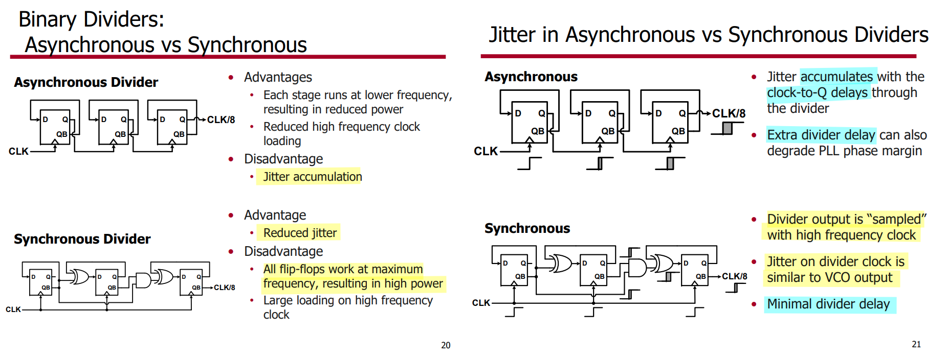
L. Romano, S. Levantino, S. Pellerano, C. Samori and A. Lacaita, "Low jitter design of a 0.35 µm-CMOS frequency divider operating up to 3GHz," Proceedings of the 28th European Solid-State Circuits Conference, Florence, Italy, 2002, pp. 611-614. [https://www.researchgate.net/publication/4158185_Low_jitter_design_of_a_035m-CMOS_frequency_divider_operating_up_to_3GHz]

loop delay effect
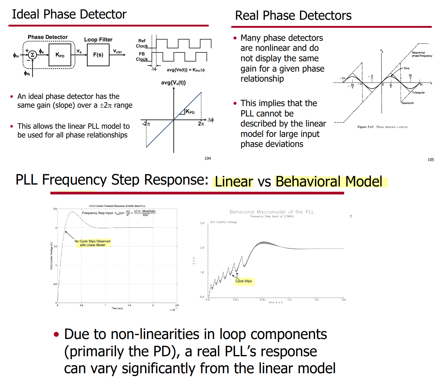
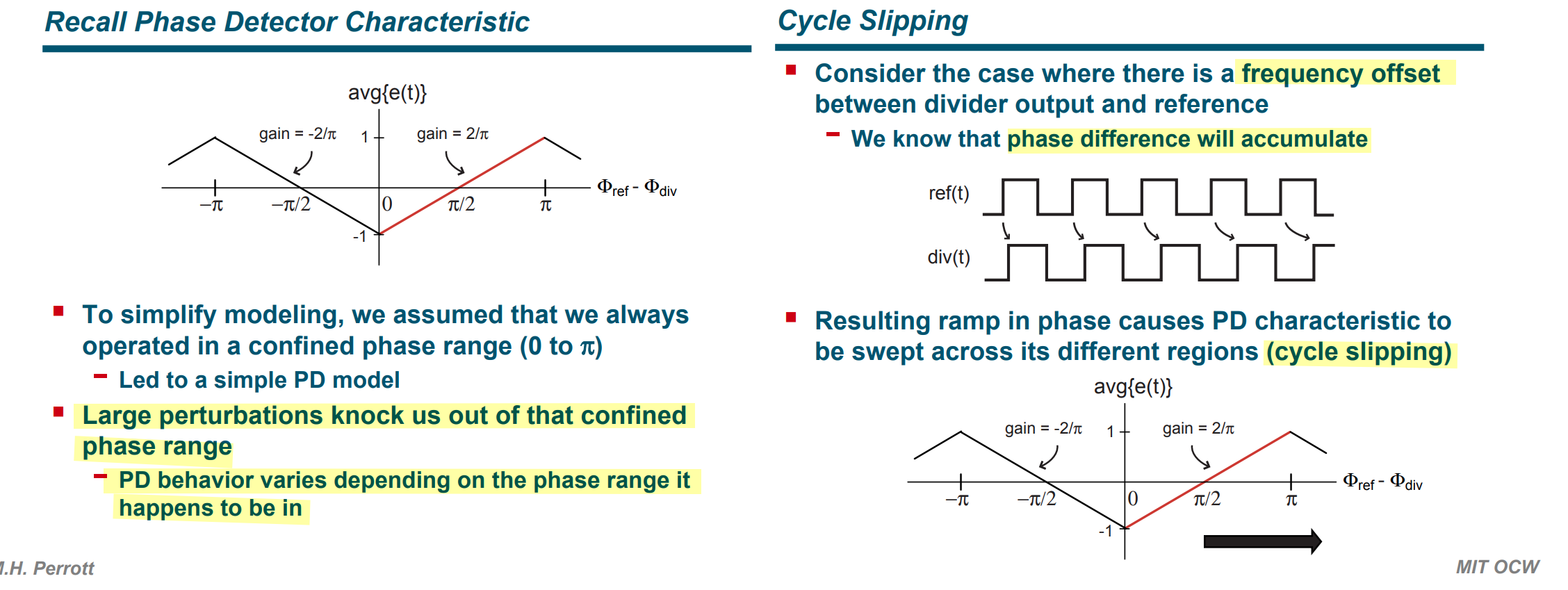
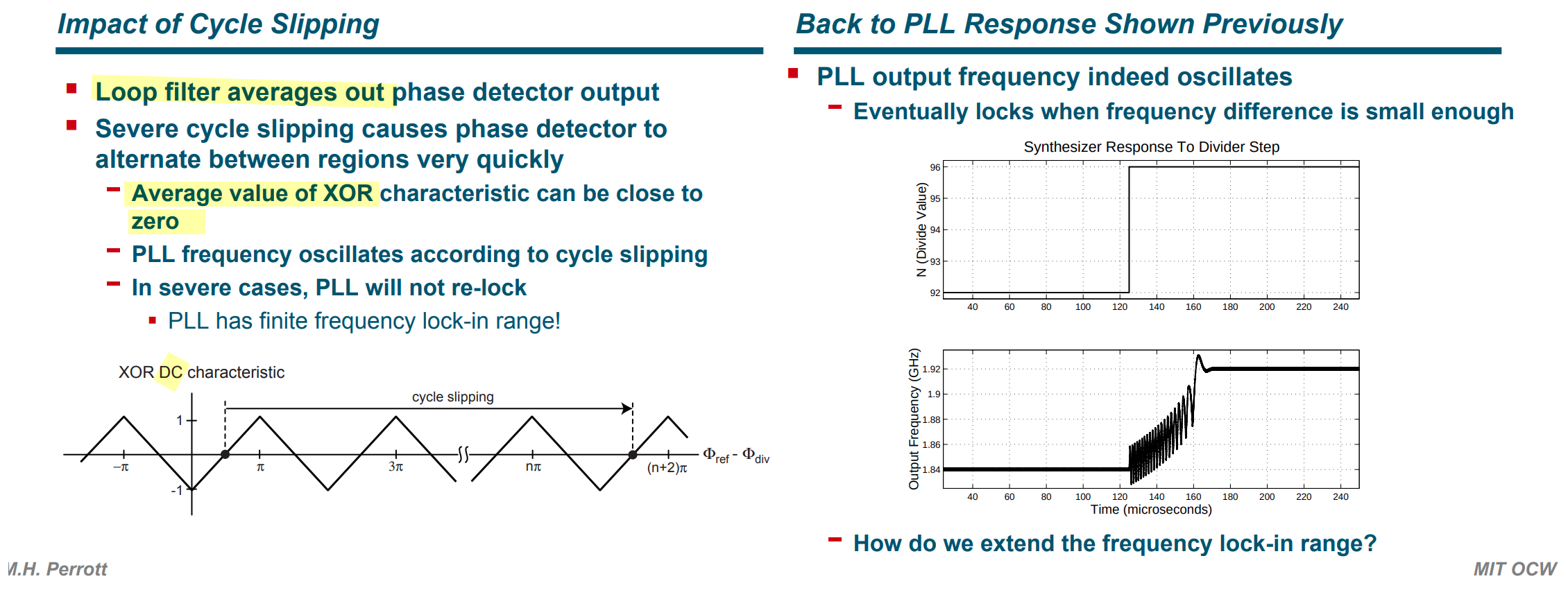
Cycle Slipping
Dennis Fischette, Could you explain the cycle-skip phenomenon in PLL performance? [https://www.delroy.com/PLL_dir/FAQ/faq_cycle_slip.txt]
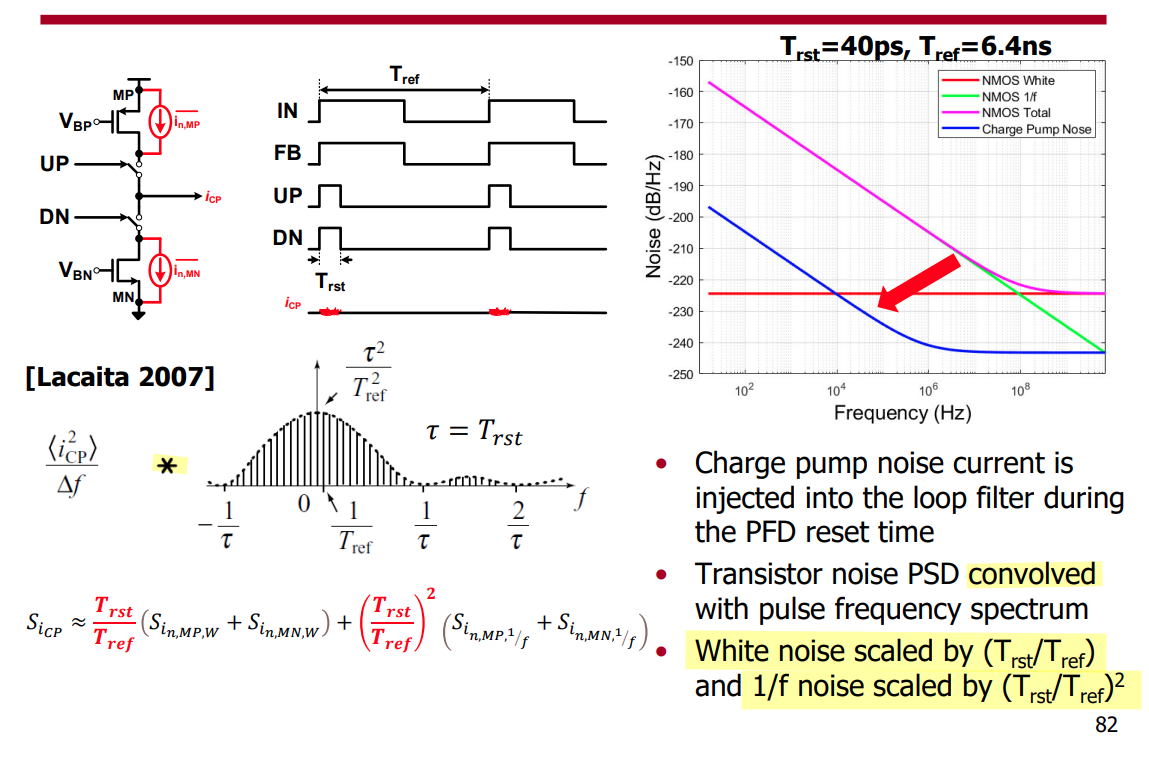
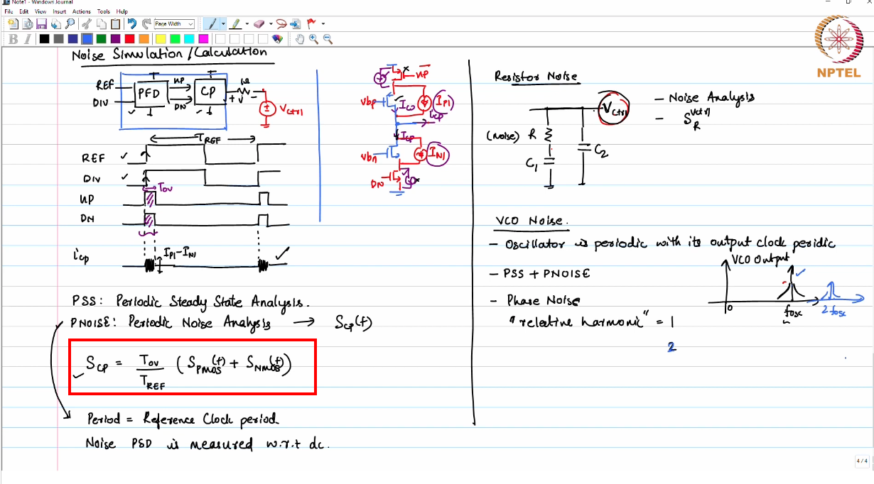
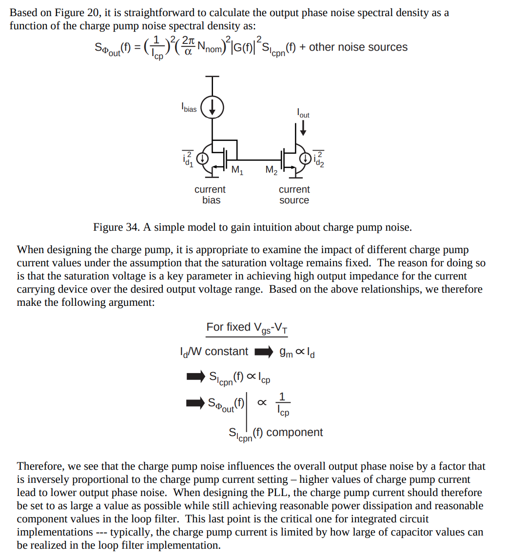
Charge Pump Noise
Cyclostationary Noise (Modulated Noise) [https://raytroop.github.io/2024/04/27/noise/#cyclostationary-noise-modulated-noise]
Sam Palermo, Lecture 3: Phase-Locked Loop Systems [https://people.engr.tamu.edu/spalermo/ecen620/lecture03_ee620_pll_system.pdf]
Saurabh Saxena,Phase Locked Loops: Noise Simulations for CP-PLL Blocks [https://youtu.be/Q1libz-XqRw]
Michael H. Perrott, PLL Design Using the PLL Design Assistant Program. [https://designers-guide.org/forum/Attachments/pll_manual.pdf]
M.H. Perrott, M.D. Trott, C.G. Sodini, "A Modeling Approach for Sigma-Delta Fractional-N Frequency Synthesizers Allowing Straightforward Noise Analysis", JSSC, vol 38, no 8, pp 1028-1038, Aug 2002. [https://www.cppsim.com/Publications/JNL/perrott_jssc02.pdf]
Non-ideal Effects in Charge Pump
Sam Palermo, Lecture 11: Clocking Architectures & PLLs [https://people.engr.tamu.edu/spalermo/ecen689/lecture11_ee720_clocking_arch_plls.pdf]
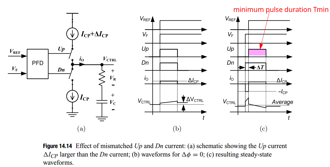
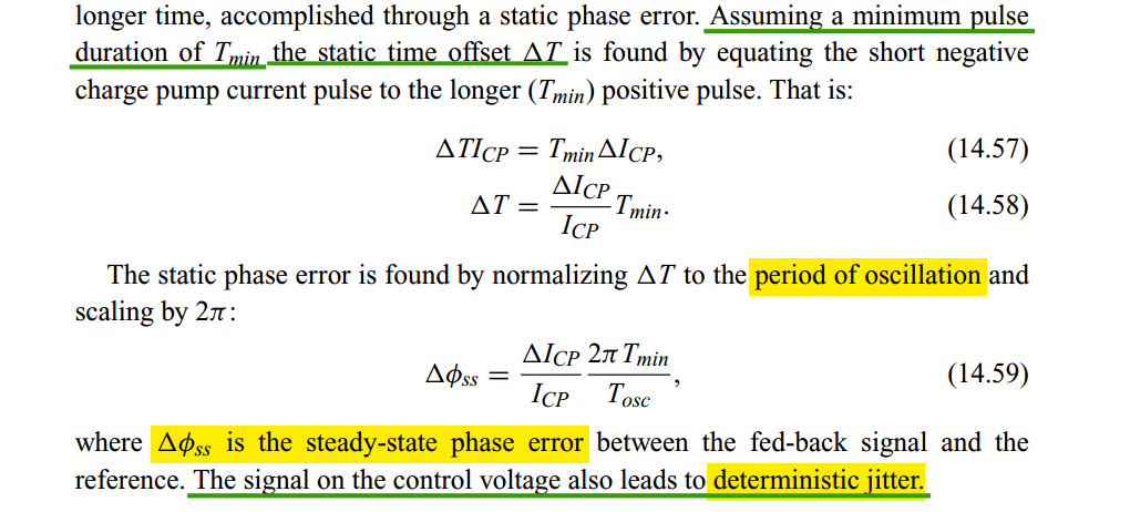
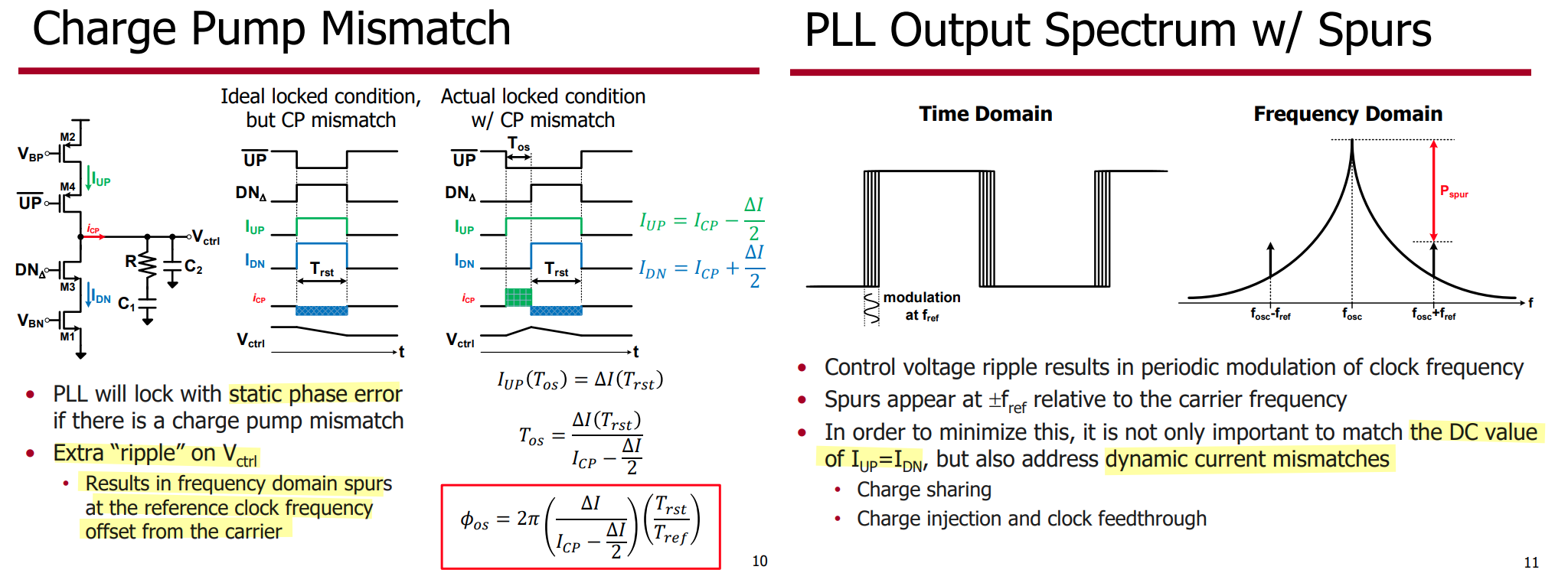
The periodic signal on VCTRL modulates the VCO, giving rise to deterministic jitter
- Timing Offsets Between Up and Dn Pulses
- Mismatch Between Charge-Pump Current Sources
- Incomplete Settling of Charge-Pump Currents
- Finite Output Resistance of the Charge Pump
Up/Dn Timing Offset
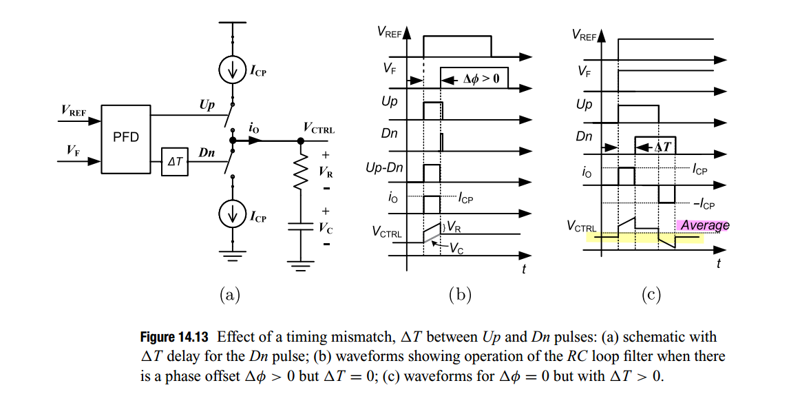
If Dn pulse arrives \(\Delta T\) after the Up pulse, the steady-state VCTRL will be slightly lower than it would be without the \(\Delta T\) mismatch so as to return the VCO's phase to match the reference clocks.
Vice versa, if If Up pulse arrives \(\Delta T\) after the Dn pulse, the steady-state VCTRL will be slightly higher than without \(\Delta T\) mismatch
Current Sources Mismatch
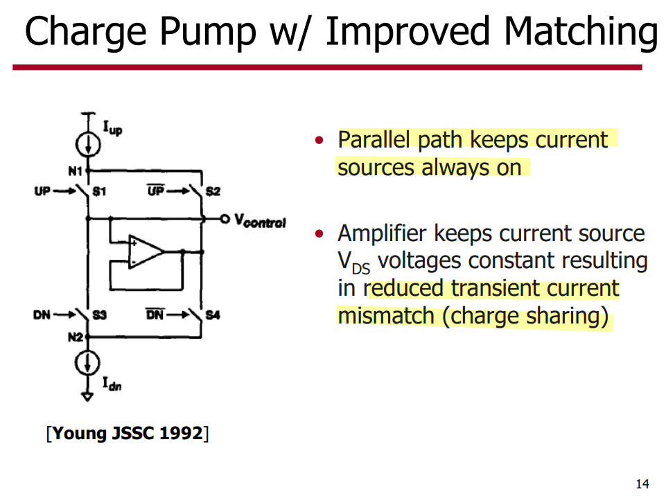
Young, I.A., Greason, J.K., Wong, K.L.: A PLL Clock Generator with 5 to 110MHz of Lock Range for Microprocessors. IEEE Journal of Solid-State Circuits 27(11), 1599– 1607 (1992) [https://people.engr.tamu.edu/spalermo/ecen620/pll_intel_young_jssc_1992.pdf]
Johnson, M., Hudson, E.: A variable delay line PLL for CPU-coprocessor synchronization. IEEE Journal of Solid-State Circuits 23(10), 1218–1223 (1988) [https://sci-hub.se/10.1109/4.5947]
Sam Palermo, Lecture 5: Charge Pump Circuits, ECEN620: Network Theory Broadband Circuit Design Fall 2024 [https://people.engr.tamu.edu/spalermo/ecen620/lecture05_ee620_charge_pumps.pdf]
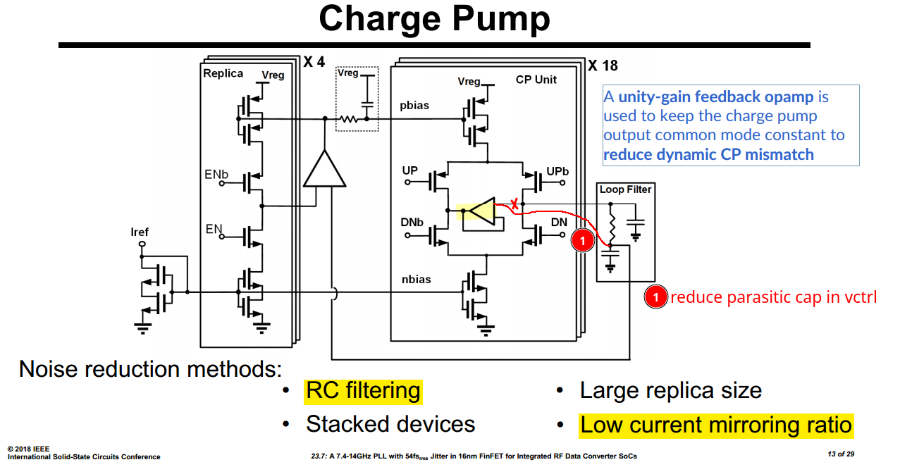
D. Turker et al., "A 7.4-to-14GHz PLL with 54fsrms jitter in 16nm FinFET for integrated RF-data-converter SoCs," 2018 IEEE International Solid-State Circuits Conference - (ISSCC), San Francisco, CA, USA, 2018 [https://sci-hub.ru/10.1109/ISSCC.2018.8310342]
charge pump with amplifier
off-state leakage
TODO 📅
Incomplete Settling
TODO 📅
W. Rhee, "Design of high-performance CMOS charge pumps in phase-locked loops," 1999 IEEE International Symposium on Circuits and Systems (ISCAS), Orlando, FL, USA, 1999, pp. 545-548 vol.2 [pdf]
Cowan G. Mixed-Signal CMOS for Wireline Communication: Transistor-Level and System-Level Design Considerations. Cambridge University Press; 2024
2nd loop filter
PI (proportional - integral) Loop Filter
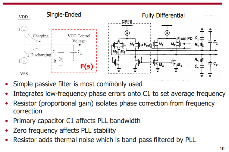
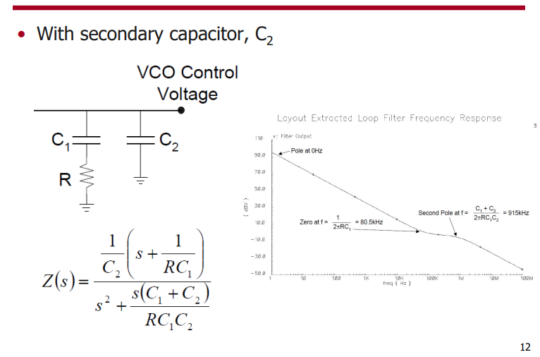
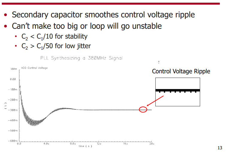
LPF leakage
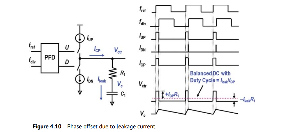
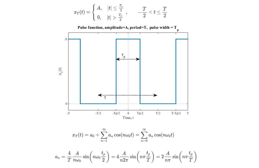
For the sake of simplicity, \(V_{ctr}\) looks like a rectangular pulse with an amplitude of \(I_{CP}R_1\) and a duty ratio of (\(I_{leak}/I_{CP}\)), whose first coefficient of Fourier series is

where \(I_\text{leak} \ll I_{CP}\) is assumed
Then, the peak frequency deviation \(\Delta f\) \[ \Delta f = a_1 \cdot K_v = 2I_\text{leak}R_1 K_v \] using narrowband FM approximation, we have \[ P_\text{spur} = 20\log\left(\frac{\Delta f}{2f_\text{ref}}\right) = 20\log\left(\frac{I_\text{leak}R_1 K_v}{f_\text{ref}}\right) \]
W. Rhee, "Design of high-performance CMOS charge pumps in phase-locked loops," 1999 IEEE International Symposium on Circuits and Systems (ISCAS), Orlando, FL, USA, 1999, pp. 545-548 vol.2 [pdf]
—. Yu, Z., 2024. Phase-Locked Loops: System Perspectives and Circuit Design Aspects. John Wiley & Sons
PFD/CP Simulation
TODO 📅
PLL Characterization
PLL bandwidth by step stimulus
[How can I experimentally find the bandwidth of my PLL?, https://dsp.stackexchange.com/a/73654/59253]
A step response test is an easy way to determine the bandwidth.
Sum a small step into the control voltage of your oscillator (VCO or NCO), and measure the 90% to 10% fall time of the corrected response at the output of the loop filter as shown in this block diagram
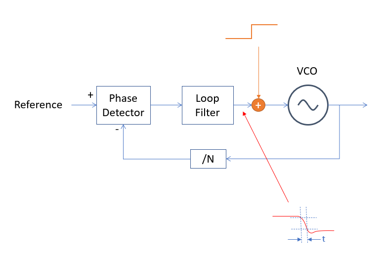
a first order loop \[ BW = \frac{0.35}{t} \space\space\space\space \text{(first order system)} \] Where \(BW\) is the 3 dB bandwidth in Hz and \(𝑡\) is the 10%/90% rise or fall time.
For second order loops with a typical damping factor of 0.7 this relationship is closer to: \[ BW = \frac{0.33}{t}\space\space\space\space \text{(second order system, damping factor = 0.7)} \]
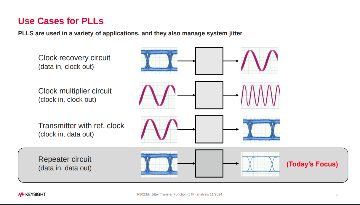
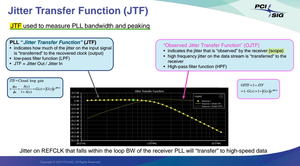
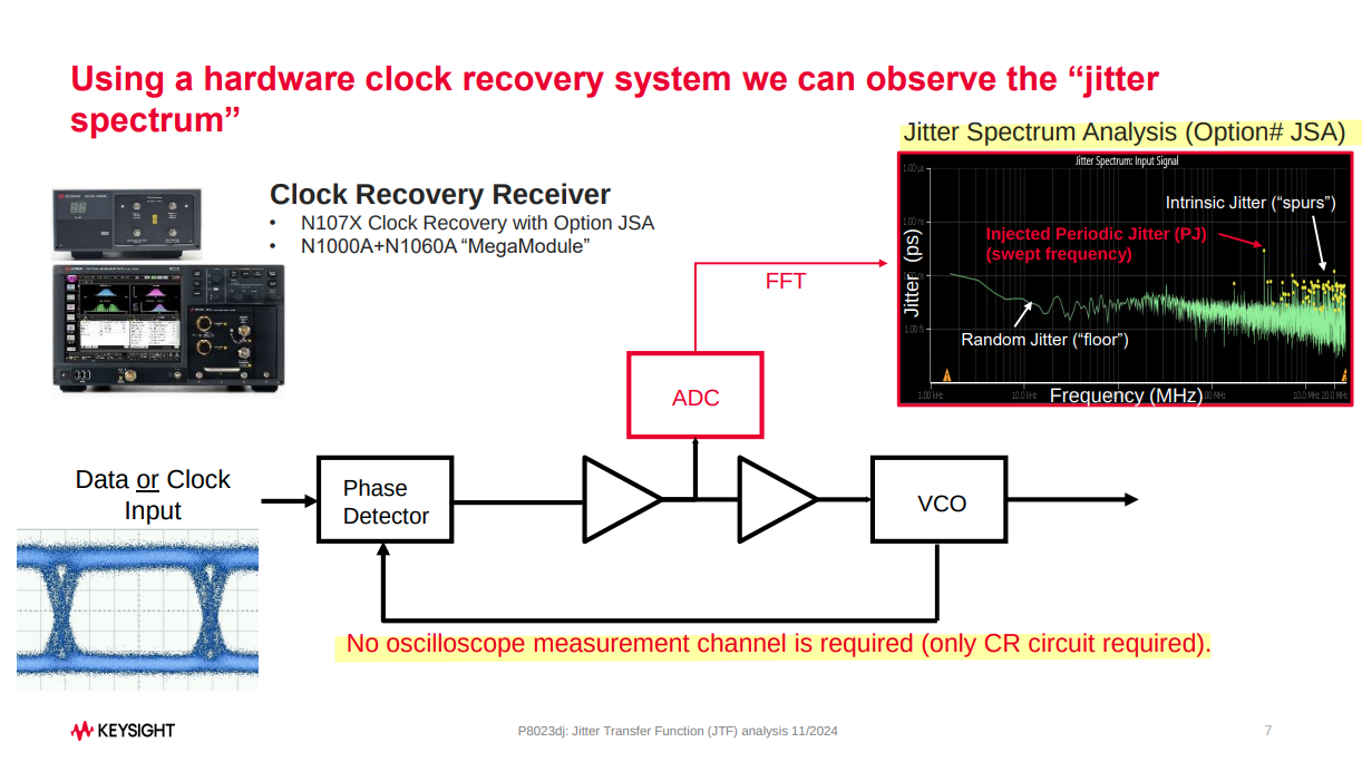
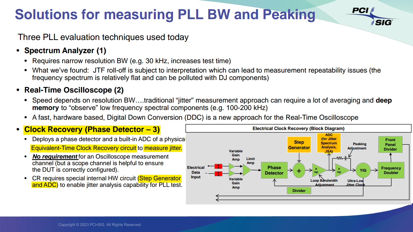
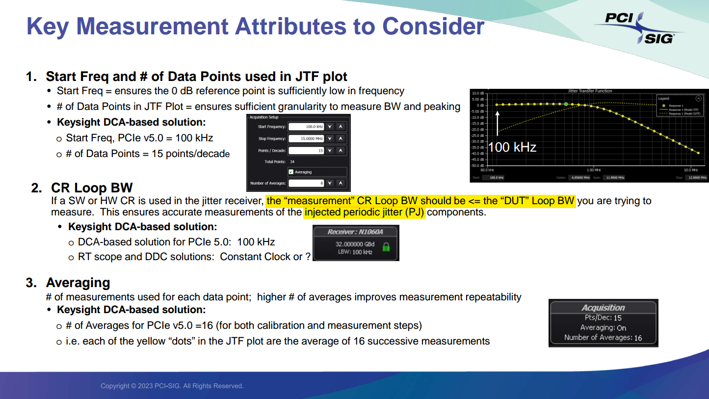
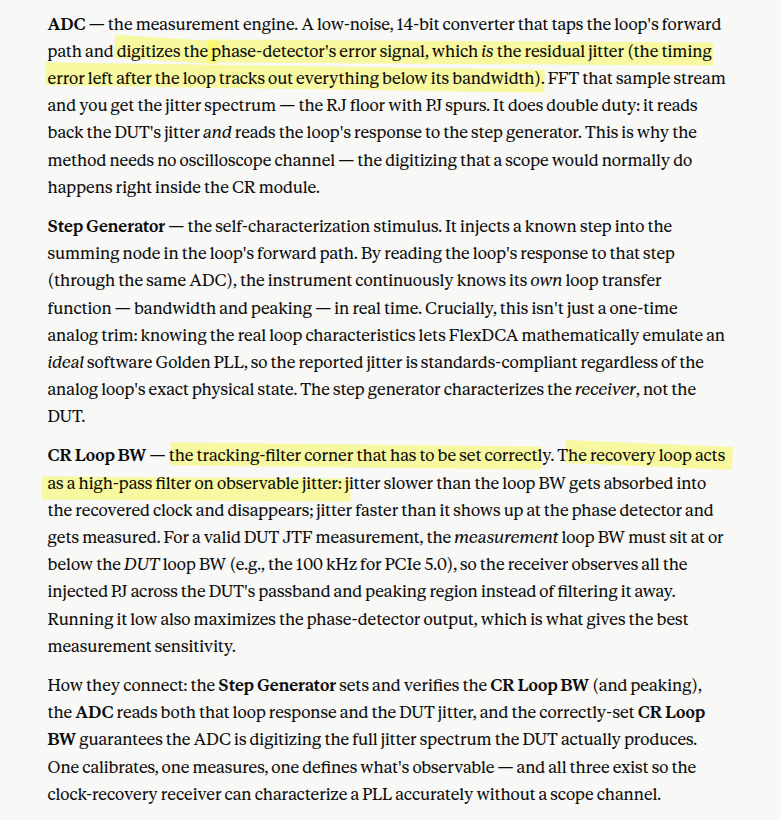
PLL BW and peaking by Clock Recovery Method
Rick Eads Principal Planner, Keysight Technologies, PLL Characterization Techniques for High Precision Measurement
John Calvin, Jitter Transfer Function (JTF) analysis Version 1.0 Presented to IEEE P802.3dj Task Force 11/11/2024 [https://grouper.ieee.org/groups/802/3/dj/public/24_11/calvin_3dj_01_2411.pdf]
Michael Schnecker, Clock Recovery Methods for Jitter Analysis [https://cdn.teledynelecroy.com/files/whitepapers/wp_clock_recovery.pdf]
—, DesignCon 2009 Jitter Transfer Measurement in Clock Circuits [https://cdn.teledynelecroy.com/files/whitepapers/designcon2009_lecroy_jitter_transfer_measurement_in_clock_circuits.pdf]
N1076B/7A/7B/8A DCA-M Optical and electric clock data recovery solutions [https://www.keysight.com/us/en/assets/7018-05291/data-sheets/5992-1620.pdf]
CP-PLL Time domain model
metroidman, fractional N量化噪声对系统相位噪声的影响 两种分析方法 LTI频域法和时域采样DFT法 [link]
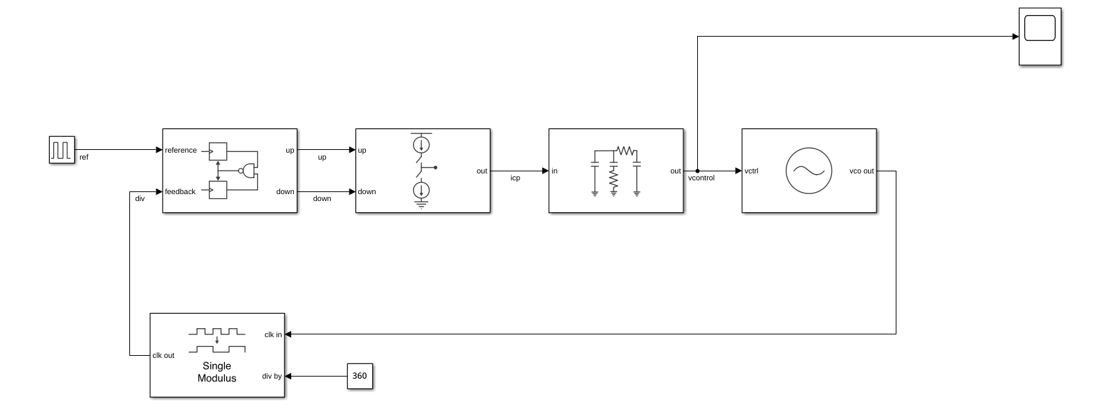
classic PLL module transient response
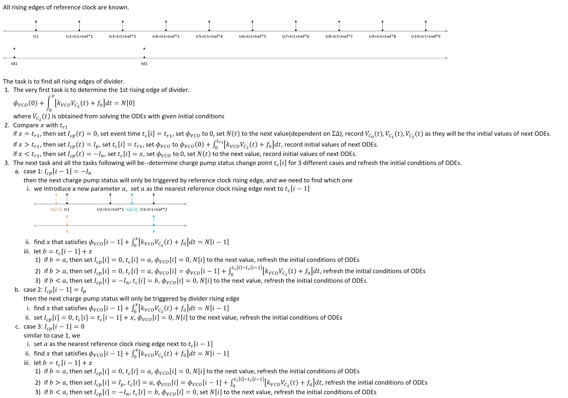
initial state is Reset
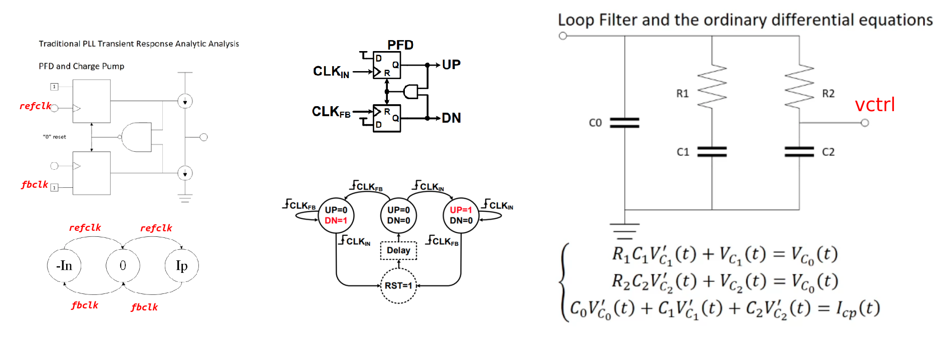
classic PLL module in Matlab & Simulink
Kai Wang, Is there a way to improve the code speed? [https://www.mathworks.com/matlabcentral/answers/2039821-is-there-a-way-to-improve-the-code-speed]
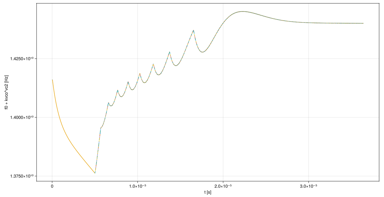
classic PLL module in Julia
Julia version (Claude Opus 4.7) [https://gist.github.com/raytroop/53f210b2cca18ec77295dc91dbe35818]
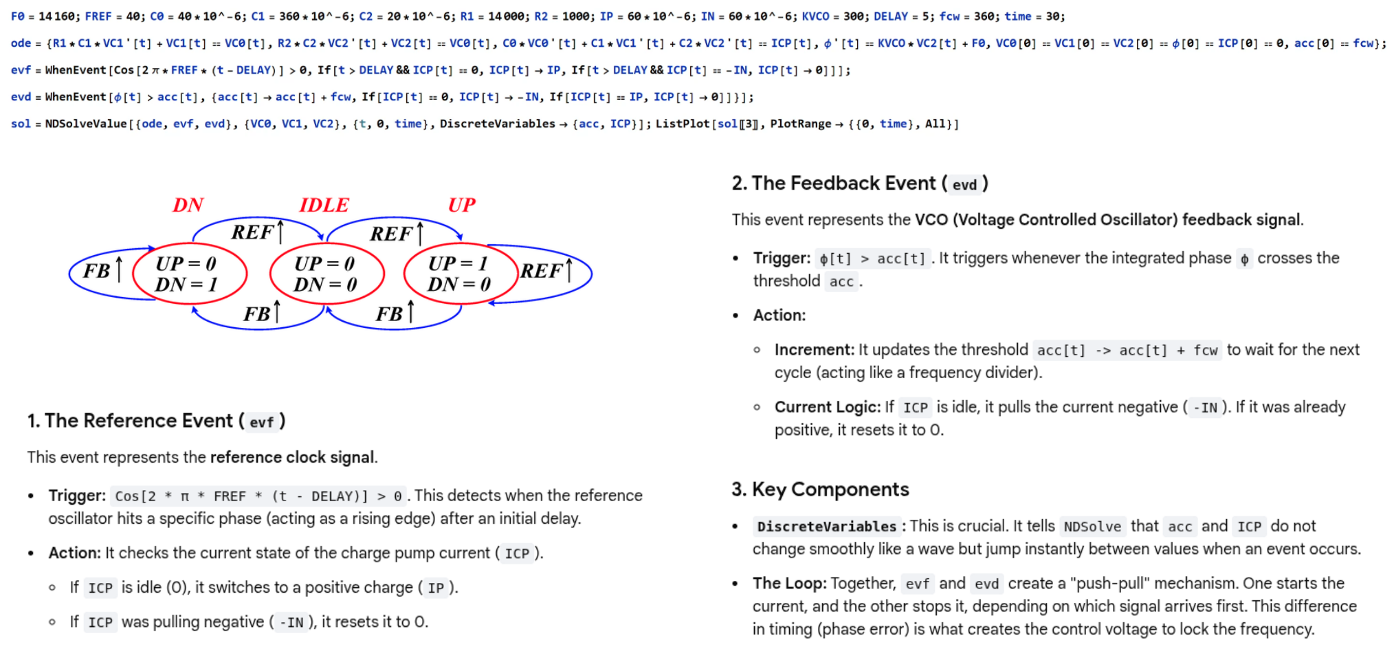
classic PLL module in Mathematica
MRDT Modeling for CP-PLL
X. Wang and S. Elsalahi, "Multi-Rate Discrete-Time Analysis and Behavioral Modeling of Nonlinear High-Order Fractional-N Charge-Pump Phase Locked Loops," in IEEE Open Journal of the Solid-State Circuits Society, doi: 10.1109/OJSSCS.2026.3737100. [https://ieeexplore.ieee.org/stamp/stamp.jsp?tp=&arnumber=11705418]
TODO 📅
Mixed-signal charge-pump PLL (dual-PDK, AMS RNM)
Ng Chuan Seng, Phase 7: Mixed-signal charge-pump PLL (dual-PDK, AMS RNM) [https://github.com/chuanseng-ng/claude_verilog_test/blob/main/docs/PHASE7_MIXED_SIGNAL_PLL_PLAN.md]
TODO 📅
reference
Lacaita, Andrea Leonardo, Salvatore Levantino, and Carlo Samori. Integrated frequency synthesizers for wireless systems. Cambridge University Press, 2007.
Saurabh Saxena. Noise Simulations for CP-PLL Blocks [https://youtu.be/Q1libz-XqRw]
—, IIT Madras. CICC2022 Clocking for Serial Links - Frequency and Jitter Requirements, Phase-Locked Loops, Clock and Data Recovery
Helene Thibieroz, Customer Support CIC. Using Spectre RF Noise-Aware PLL Methodology to Predict PLL Behavior Accurately [https://citeseerx.ist.psu.edu/document?repid=rep1&type=pdf&doi=3056e59ea76165373f90152f915a829d25dabebc]
Chembiyan T. Chargepump PLL Basics- From A Control Theoretic Viewpoint [linkedin]
—. Challenges in Chargepump PLL Design- A Qualitative Approach [linkedin]
—. A Unified Approach to Low Noise Loop Design in Chargepump PLLs [linkedin]
N. Kuznetsov, A. Matveev, M. Yuldashev and R. Yuldashev, "Nonlinear Analysis of Charge-Pump Phase-Locked Loop: The Hold-In and Pull-In Ranges," in IEEE Transactions on Circuits and Systems I: Regular Papers, vol. 68, no. 10, pp. 4049-4061, Oct. 2021 [https://ieeexplore.ieee.org/stamp/stamp.jsp?arnumber=9509840]
Xiang Gao Credo Semiconductor. ISSCC2018 T1: Low-Jitter PLLs for Wireless Transceivers