Receiver Front Ends
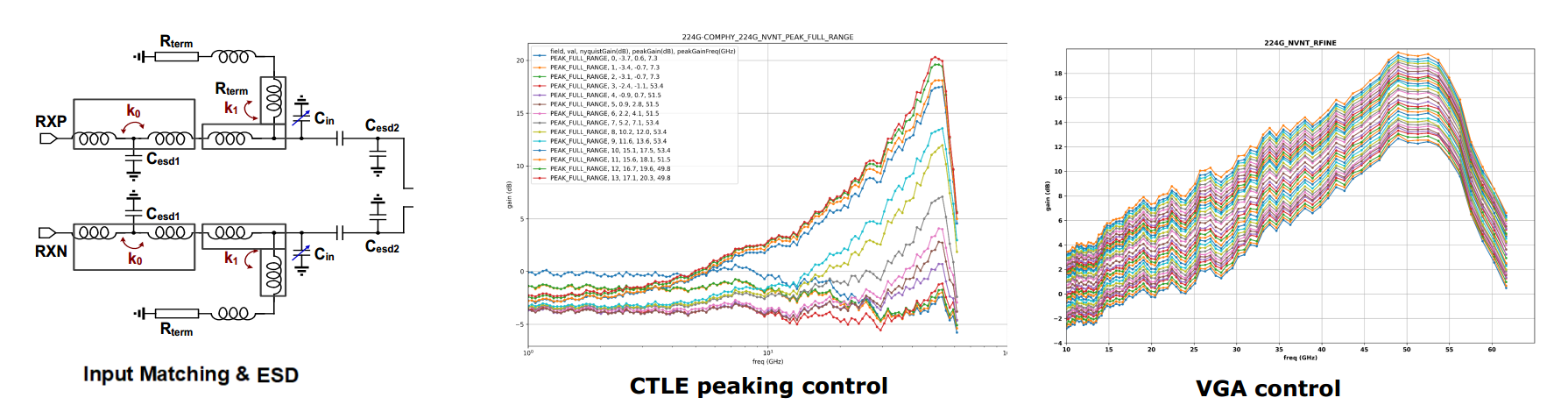
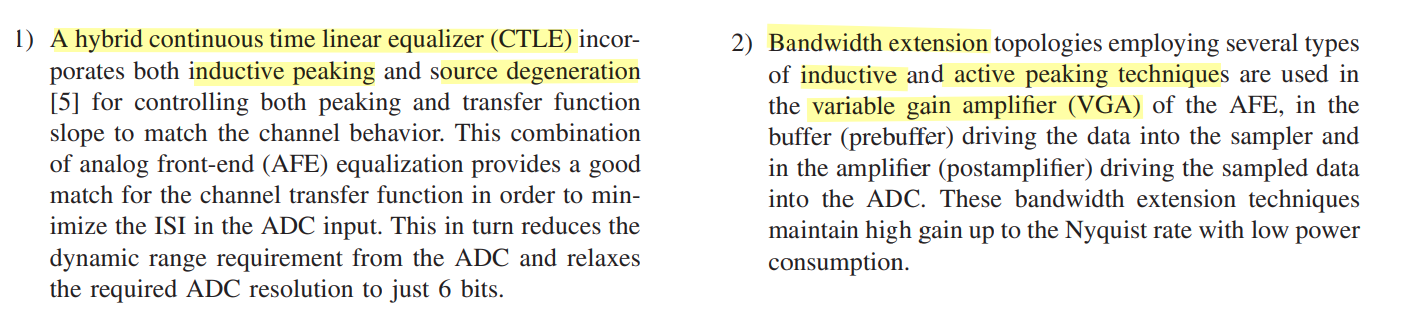
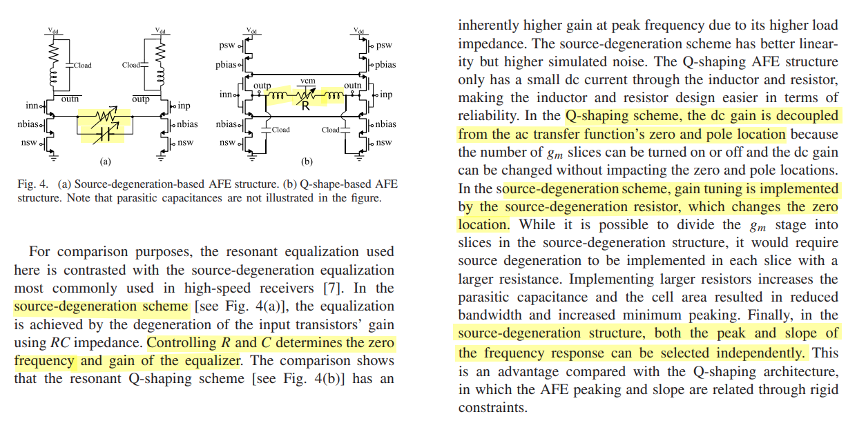
source-degeneration -> +resonator-based CTLE for higher peaking frequency
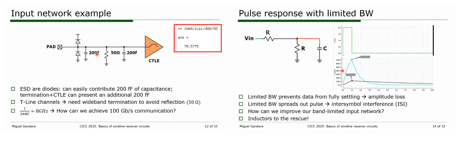
input network
2
3
4
5
ans =
79.5775
CTLE design target
peaking gain + curve shape
CTLE transfer function
Circuit Insights @ ISSCC2025: Circuits for Wireline Communications - Kevin Zheng [https://youtu.be/8NZl81Dj45M&t=1045]
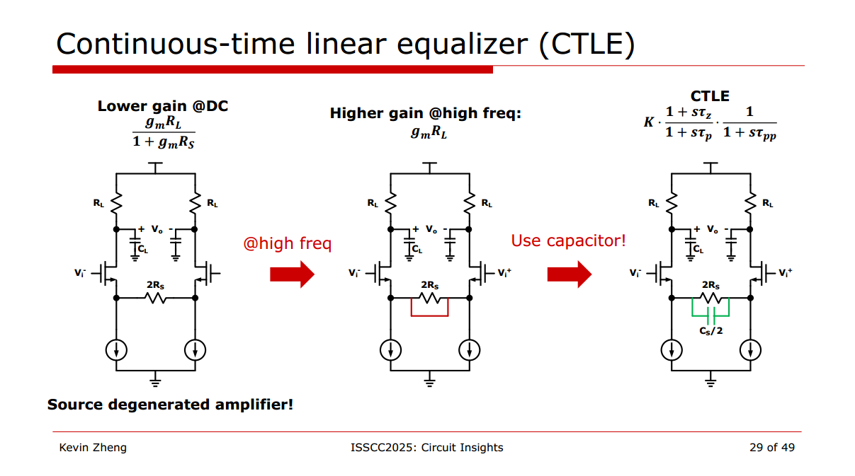
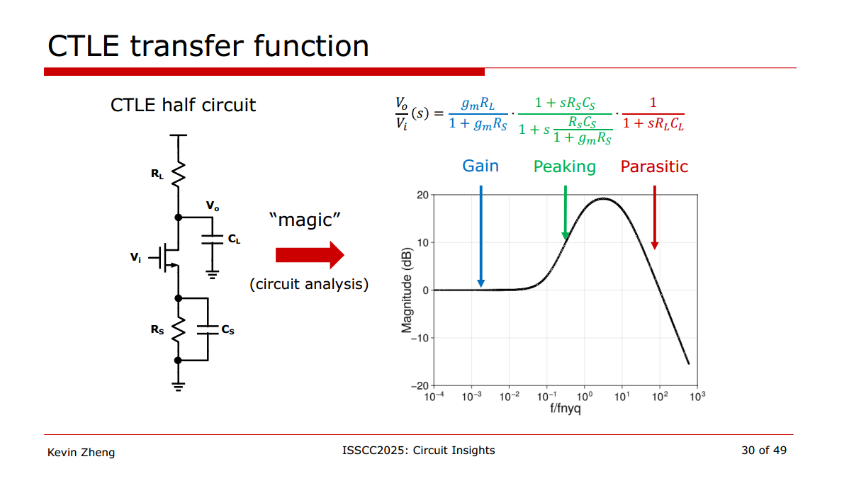
Why Shunt-peaking or Source Degenerated type Active CTLE? [https://youtu.be/EFMZG-FIWeo]
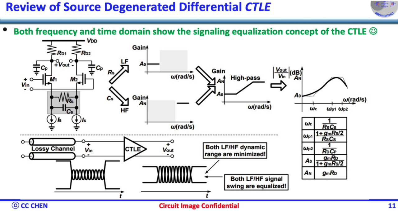
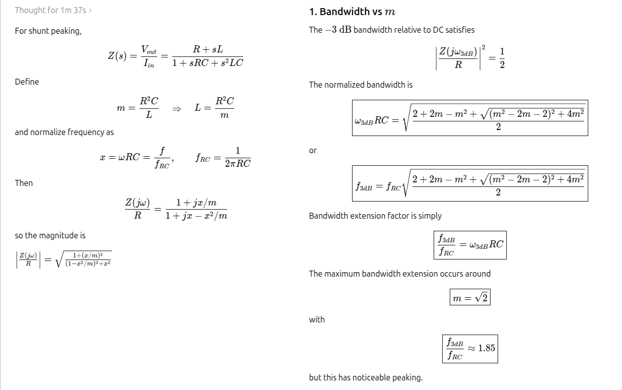
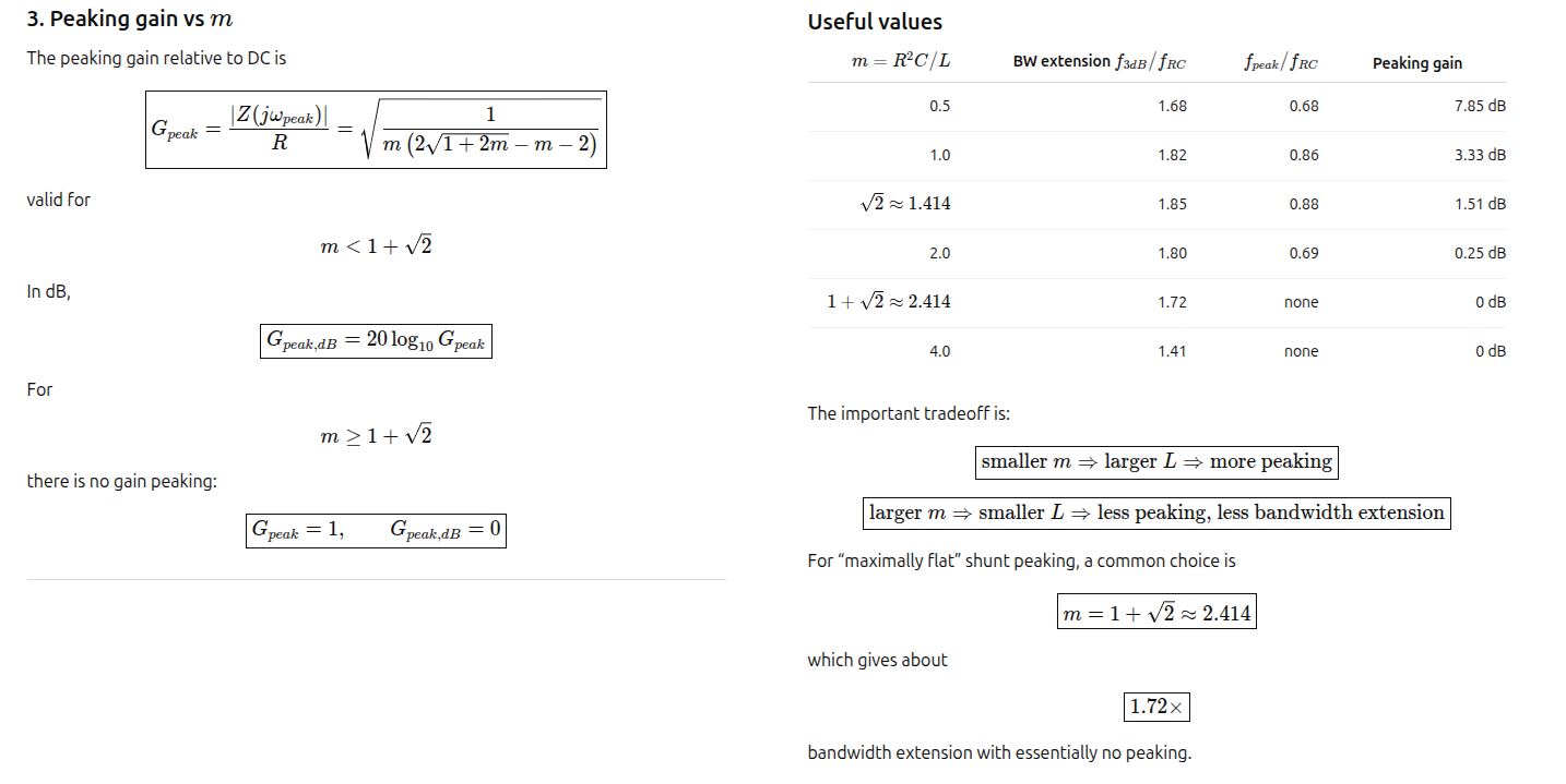
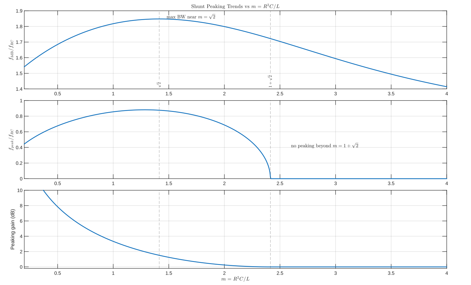
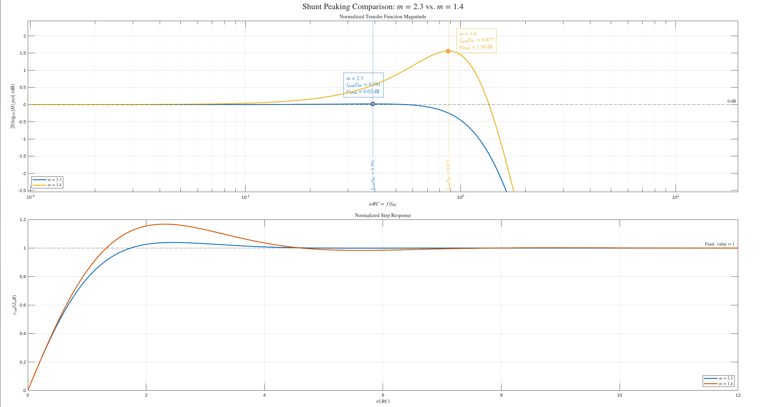
Shunt Peaking broaden the RC bandwidth
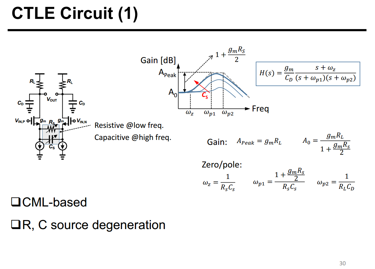
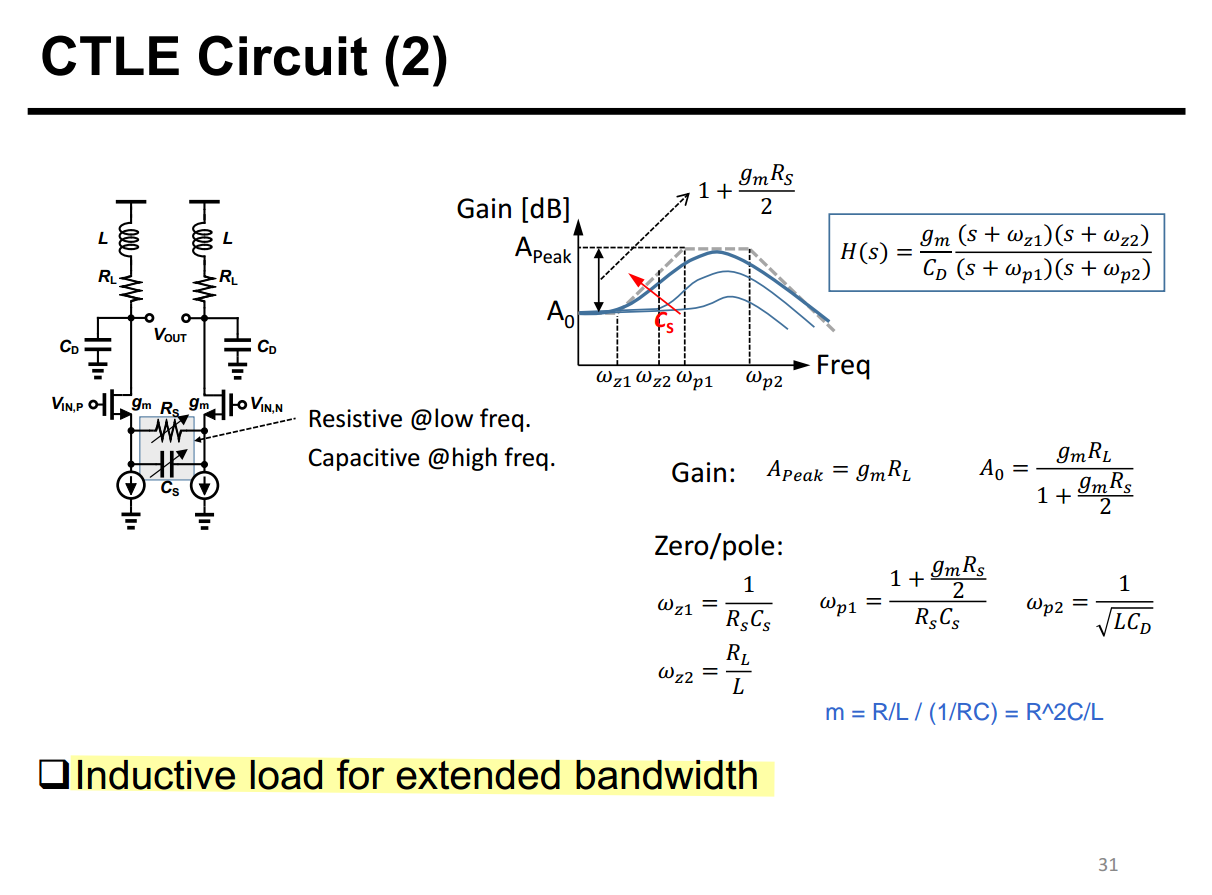
curve shape
PCIe Gen6 Channel and Reference Package S4P Models for Rx Stressed Eye Calibration
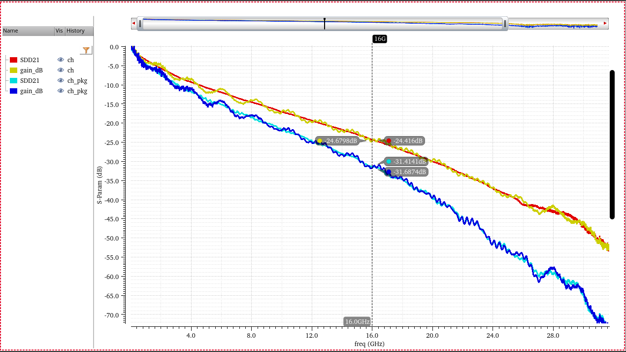
Above curve demonstrate that only zero is not enough to compensate channel+pkg loss (>20 dB/decade), peaking or Complex-Conjugate Poles is necessary

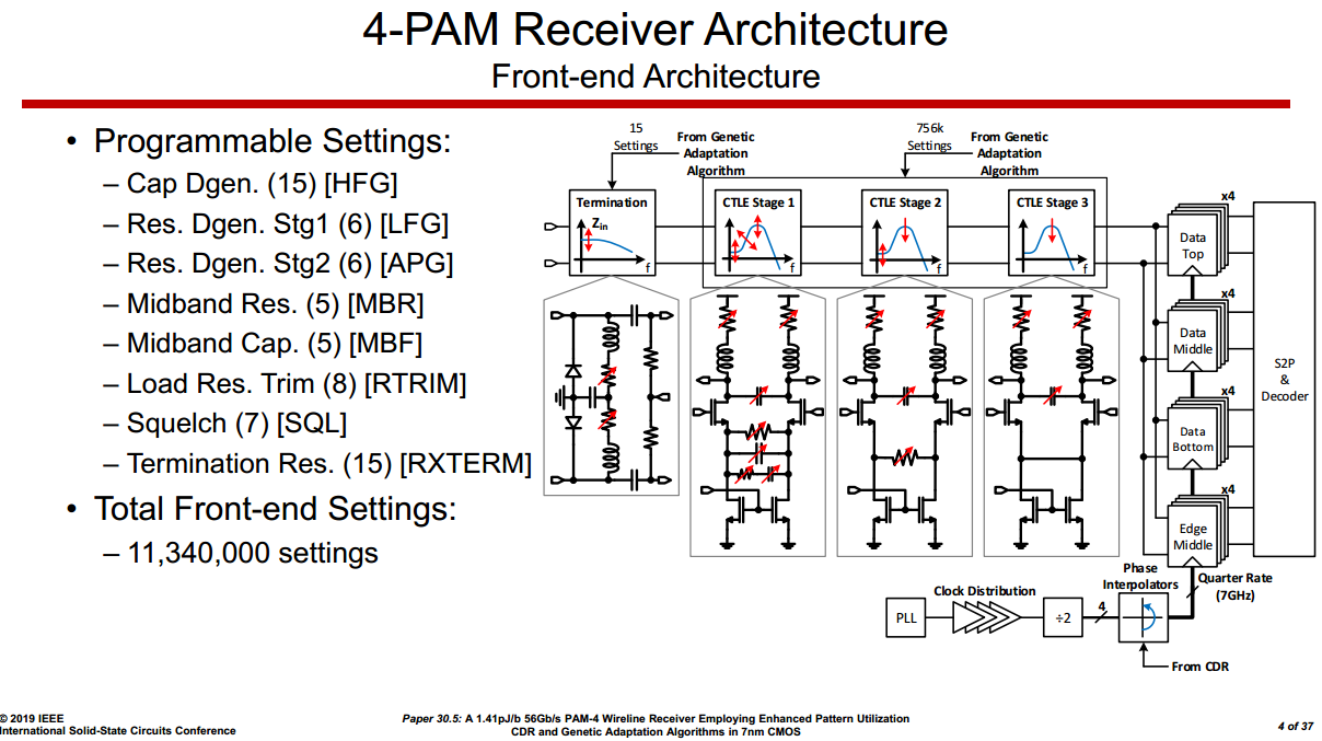
S. Shahramian et al., "30.5 A 1.41pJ/b 56Gb/s PAM-4 Wireline Receiver Employing Enhanced Pattern Utilization CDR and Genetic Adaptation Algorithms in 7nm CMOS," 2019 IEEE International Solid-State Circuits Conference - (ISSCC), San Francisco, CA, USA, 2019 [pdf]
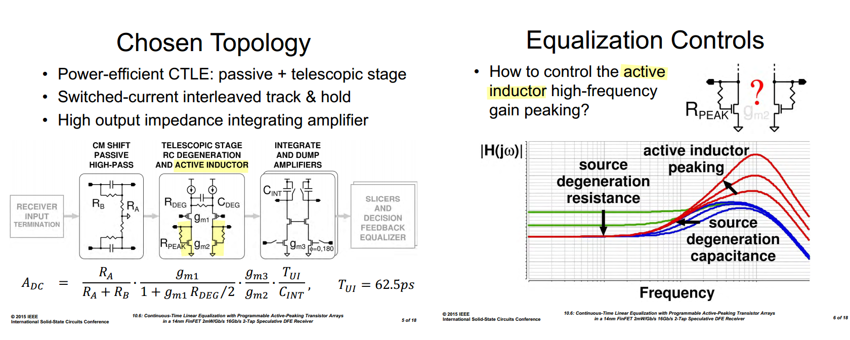
P. A. Francese et al., "10.6 continuous-time linear equalization with programmable active-peaking transistor arrays in a 14nm FinFET 2mW/Gb/s 16Gb/s 2-Tap speculative DFE receiver," 2015 IEEE International Solid-State Circuits Conference - (ISSCC) Digest of Technical Papers, San Francisco, CA, USA, 2015 [https://sci-hub.se/10.1109/ISSCC.2015.7062988]
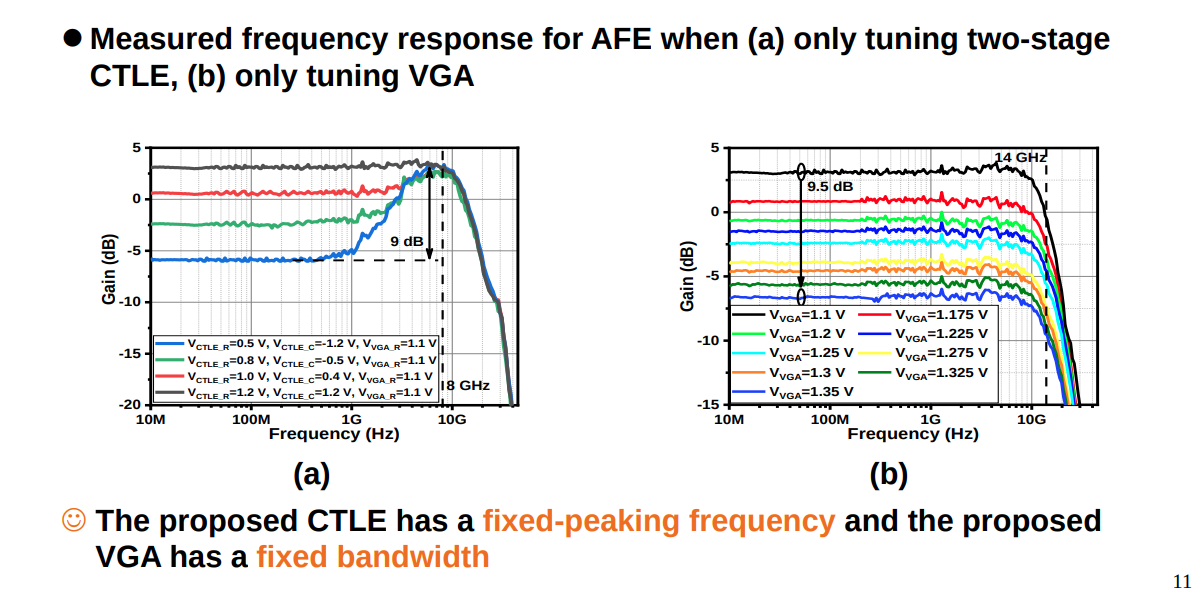
Z. Li, M. Tang, T. Fan and Q. Pan, "A 56-Gb/s PAM4 Receiver Analog Front-End With Fixed Peaking Frequency and Bandwidth in 40-nm CMOS," in IEEE Transactions on Circuits and Systems II: Express Briefs, vol. 68, no. 9, pp. 3058-3062, Sept. 2021 [slides] [paper]
In the active copper cable (ACC) application, it is necessary to give different equalizations at the same frequency according to different cable lengths, Therefore, the AFE with fixed peaking frequency and constant bandwidth is desirable for these applications
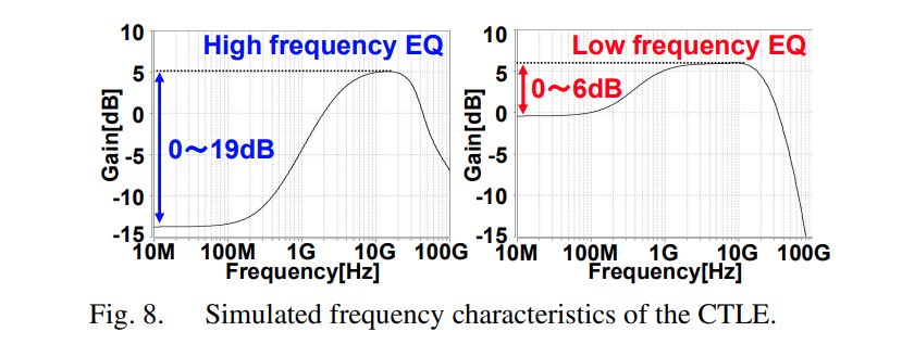
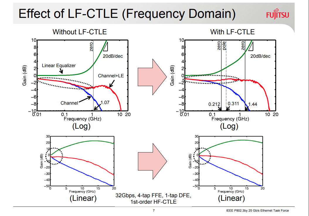
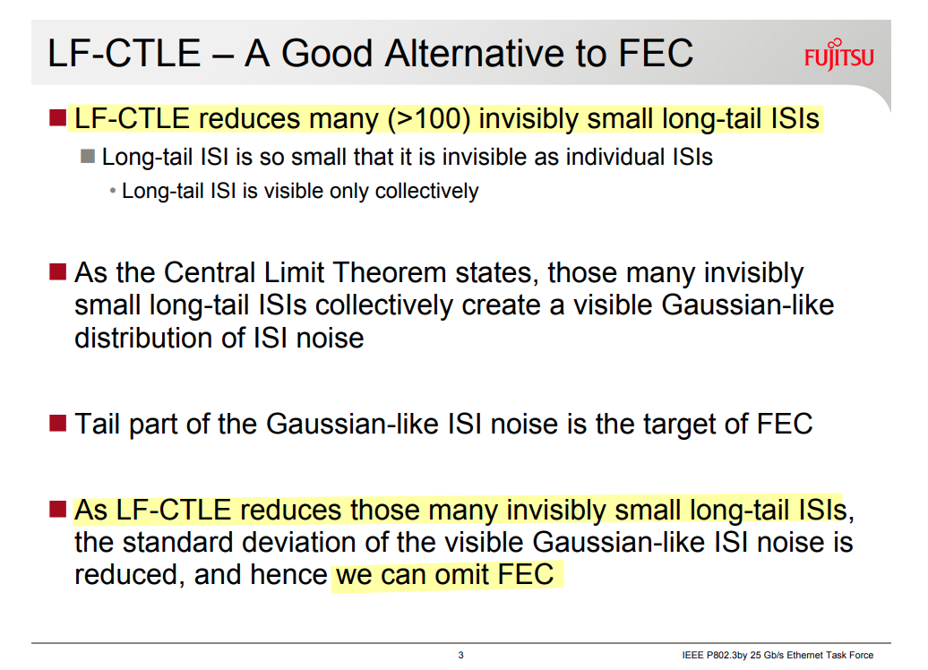
Low-Frequency CTLE (LF-CTLE)
S. Parikh et al., "A 32Gb/s wireline receiver with a low-frequency equalizer, CTLE and 2-tap DFE in 28nm CMOS," 2013 IEEE International Solid-State Circuits Conference Digest of Technical Papers, San Francisco, CA, USA, 2013 [https://sci-hub.se/10.1109/ISSCC.2013.6487622]
T. Shibasaki et al., "A 56-Gb/s receiver front-end with a CTLE and 1-tap DFE in 20-nm CMOS," 2014 Symposium on VLSI Circuits Digest of Technical Papers, Honolulu, HI, USA, 2014, pp. 1-2
Yasuo Hidaka Comment #146, #174: Low-Frequency CTLE to support 3m cable w/o FEC [https://www.ieee802.org/3/by/public/Sept15/hidaka_3by_01_0915.pdf]
Equalization Noise Enhancement
Advanced Signal Integrity for High-Speed Digital Designs, S. H. Hall and H. L. Heck, John Wiley & Sons, 2009
CC Chen, Why CTLE? [https://youtu.be/zsuJMqadaKY]
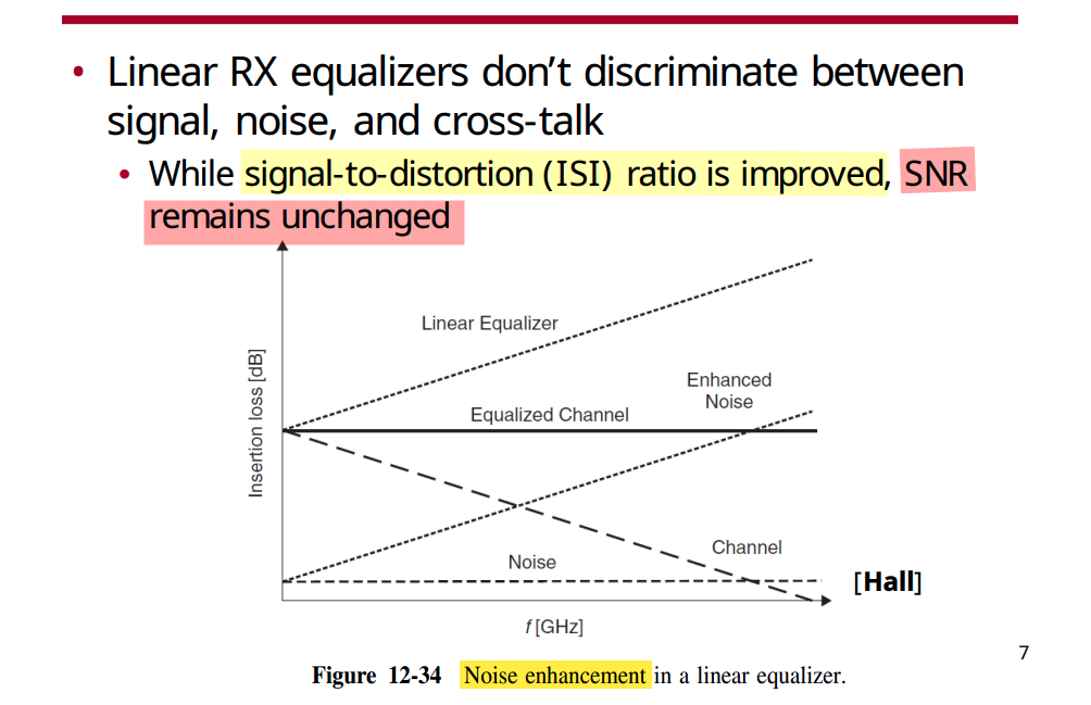
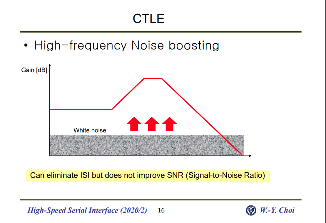
Assuming \(\mathrm{SNR}(f) = \frac{S_x(f)}{S_n(f)}\)
trade-offs between noise amplification and signal equalization
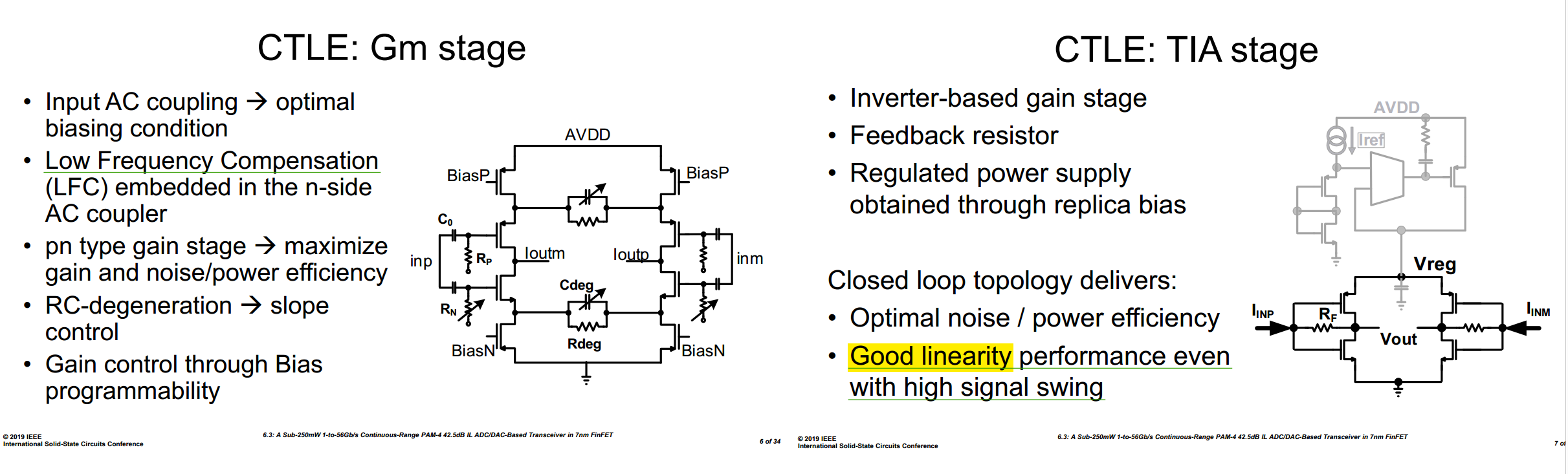
Gm-TIA
H. Kimura et al., "A 28 Gb/s 560 mW Multi-Standard SerDes With Single-Stage Analog Front-End and 14-Tap Decision Feedback Equalizer in 28 nm CMOS," in IEEE Journal of Solid-State Circuits, vol. 49, no. 12, pp. 3091-3103, Dec. 2014 [https://ieeexplore.ieee.org/ielx7/4/6963535/06894632.pdf]
Pisati, et.al., "Sub-250mW 1-to-56Gb/s Continuous-Range PAM-4 42.5dB IL ADC/DAC- Based Transceiver in 7nm FinFET," 2019 IEEE International Solid-State Circuits Conference (ISSCC), 2019 [https://sci-hub.se/10.1109/ISSCC.2019.8662428]
Z. Li, M. Tang, T. Fan and Q. Pan, "A 56-Gb/s PAM4 Receiver Analog Front-End With Fixed Peaking Frequency and Bandwidth in 40-nm CMOS," in IEEE Transactions on Circuits and Systems II: Express Briefs, vol. 68, no. 9, pp. 3058-3062, Sept. 2021 [slides] [paper]
K. Kwon et al., "A 212.5Gb/s Pam-4 Receiver With Mutual Inductive Coupled Gm-Tia in 4nm Finfet," 2025 Symposium on VLSI Technology and Circuits (VLSI Technology and Circuits), Kyoto, Japan, 2025
Bae, W. (2019). CMOS Inverter as Analog Circuit: An Overview. Journal of Low Power Electronics and Applications. [pdf]
CTLE, with Gm + TIA structure
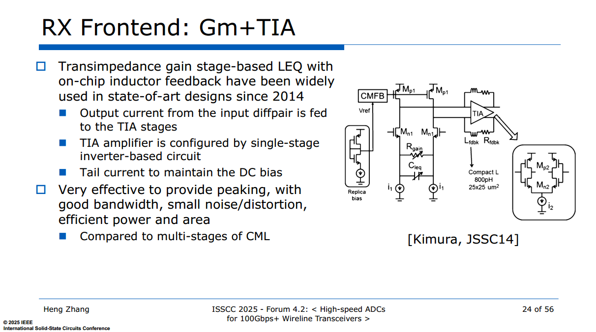
Chongyun ZHANG, 2025, "Energy-Efficient CMOS Optical Receiver for Short-Reach Data Center Application,". [slides, paper]
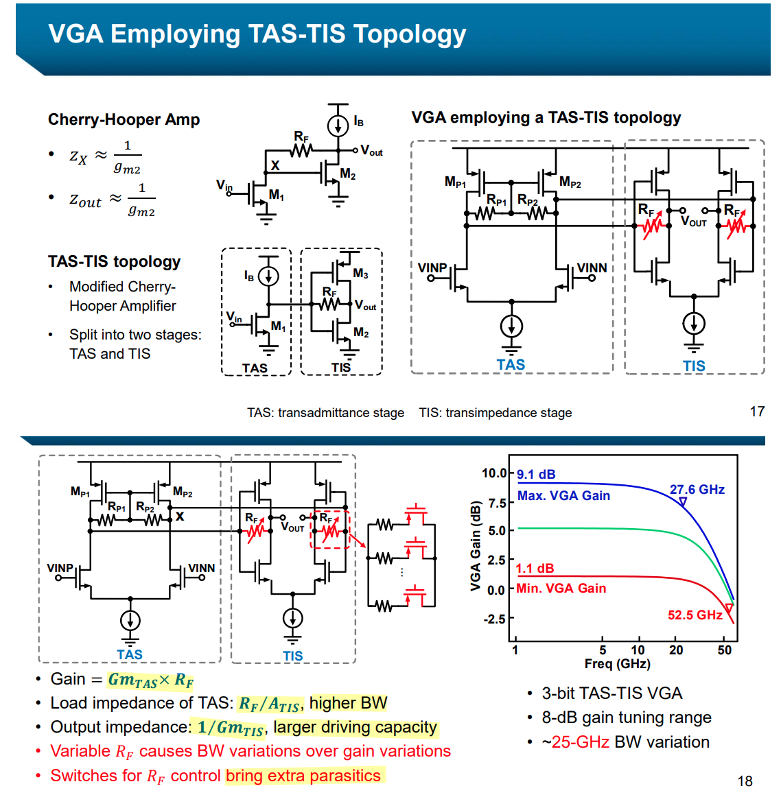
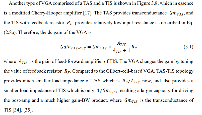
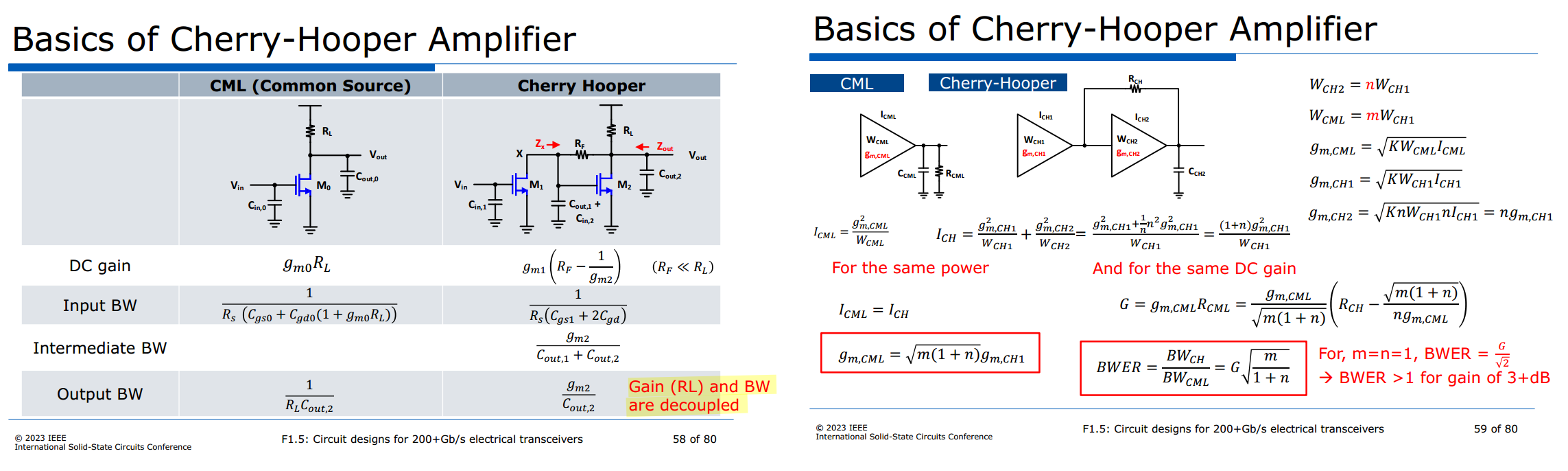
Cherry-Hooper Amplifier
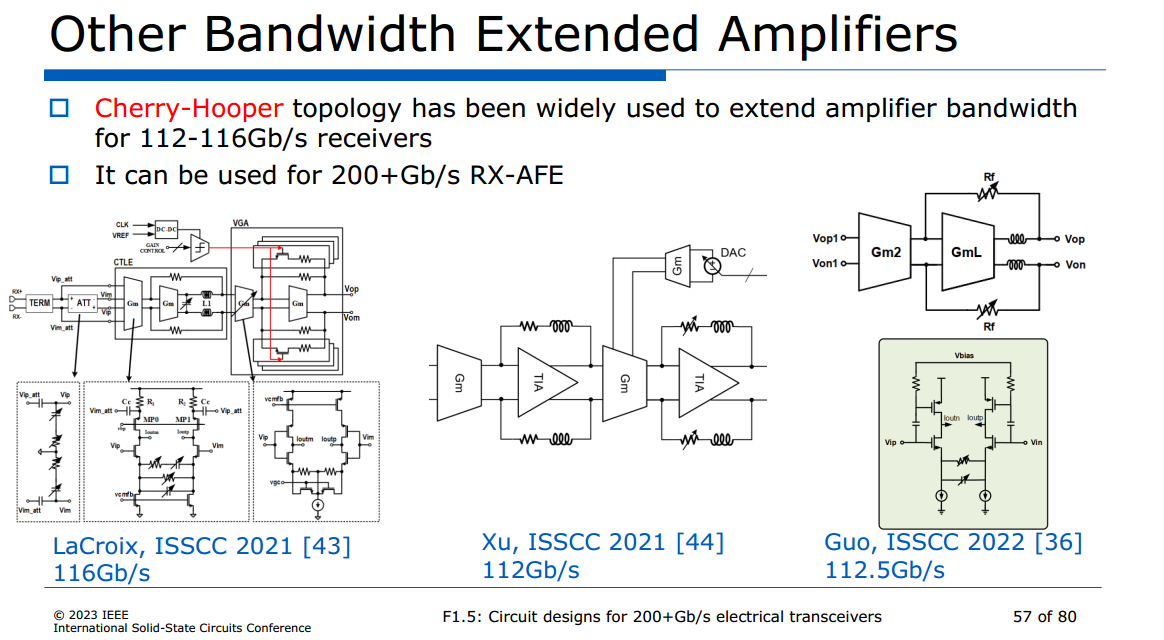
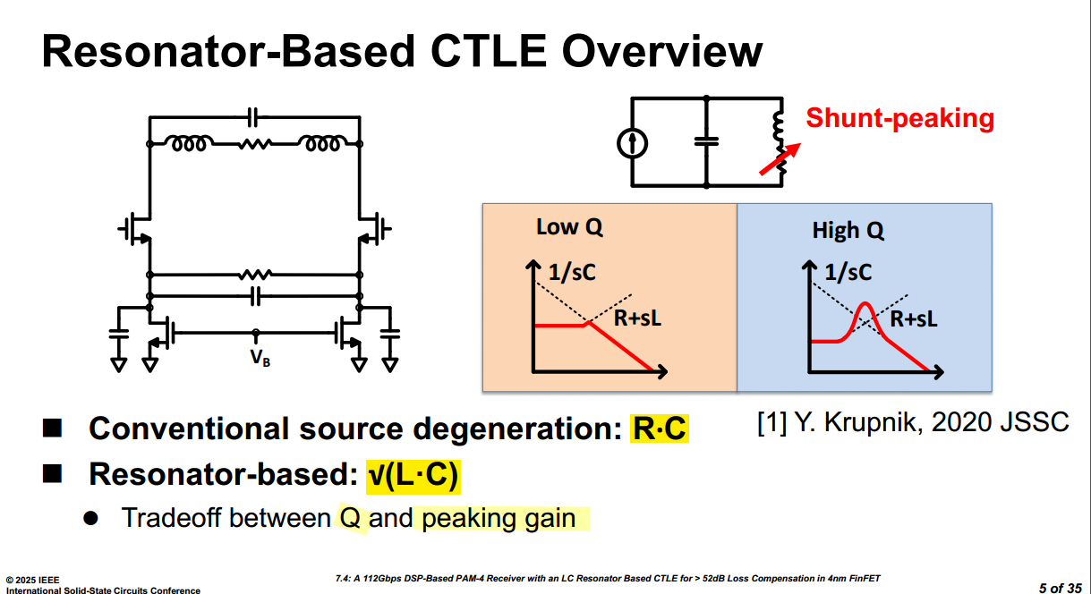
Resonator-Based CTLE
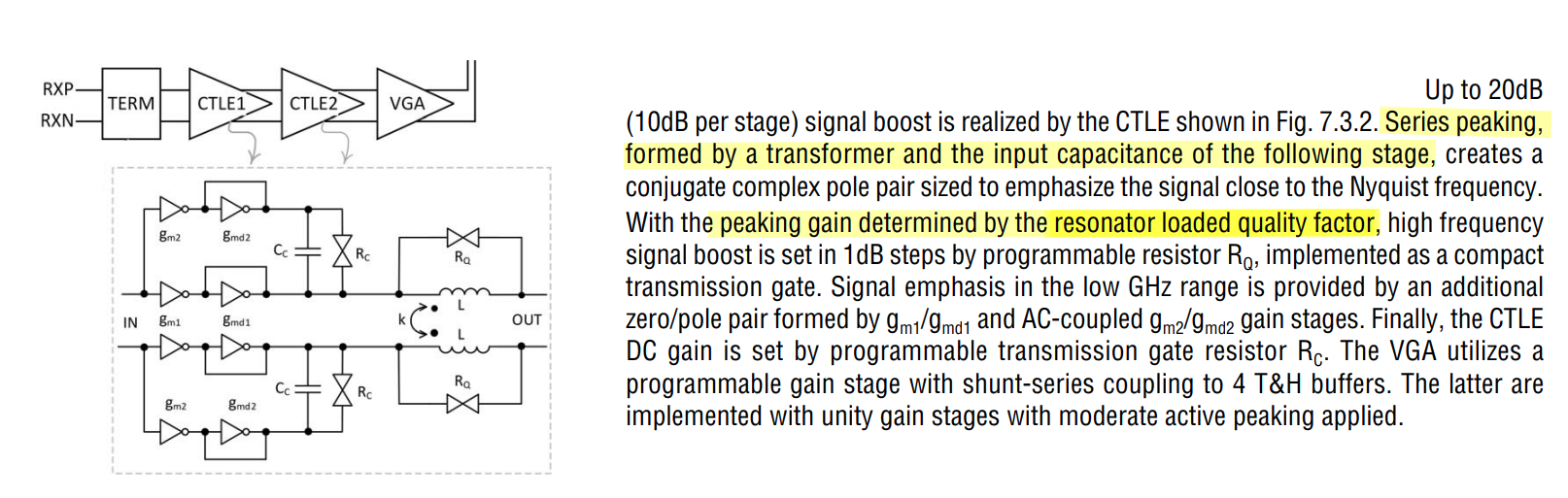
Passive series peaking
D. Pfaff et al., "7.3 A 224Gb/s 3pJ/b 40dB Insertion Loss Transceiver in 3nm FinFET CMOS," 2024 IEEE International Solid-State Circuits Conference (ISSCC), San Francisco, CA, USA, 2024, pp. 128-130, doi: 10.1109/ISSCC49657.2024.10454537.
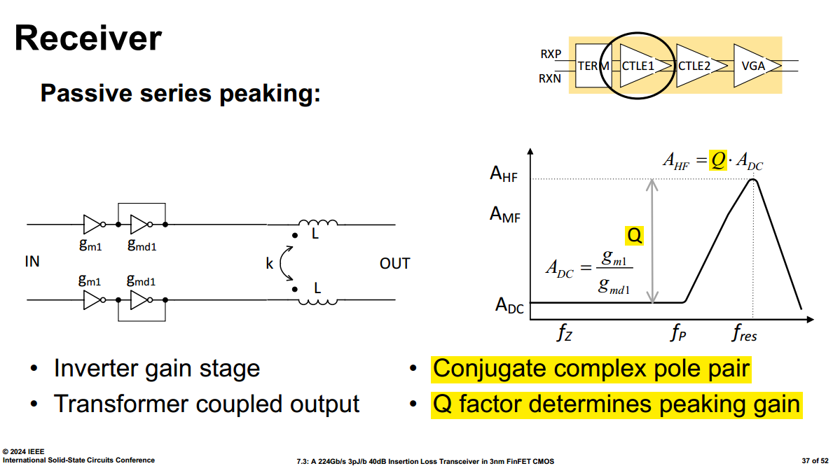
At DC \[ i_f = g_{md1}v_f \quad i_f = (v_f - v_o)/R_f \qquad \Longrightarrow \qquad \frac{v_o}{v_i} = -\frac{g_{m1}}{g_{md1}} + g_{m1}R_f \] since \(R_f=0\) \[ A_{DC} = -\frac{g_{m1}}{g_{md1}} \]

\[ \frac{V_o}{V_i}(s) = -g_{m1}R_s\cdot \frac{\frac{1}{LC}}{s^2 + \frac{R_s+R_{LS}}{L}s + \frac{1}{LC}}=-g_{m1}R_s\cdot \frac{\omega_n^2}{s^2+\frac{\omega_n}{Q}s+\omega_n^2} \]
where \[ \boxed{Q=\frac{\omega_n L}{R_s + R_{LS}} \qquad \qquad \omega_n = \frac{1}{\sqrt{LC}}} \]
The \(Q\) is the resonator loaded quality factor
That is \[ A_{DC}=-g_{m1}R_s\qquad\qquad A_{HF}=jg_{m1}R_s\cdot Q \qquad\qquad \frac{A_{HF}}{A_{DC}} = Q \]
where \(A_{HF}\) is the gain at resonance
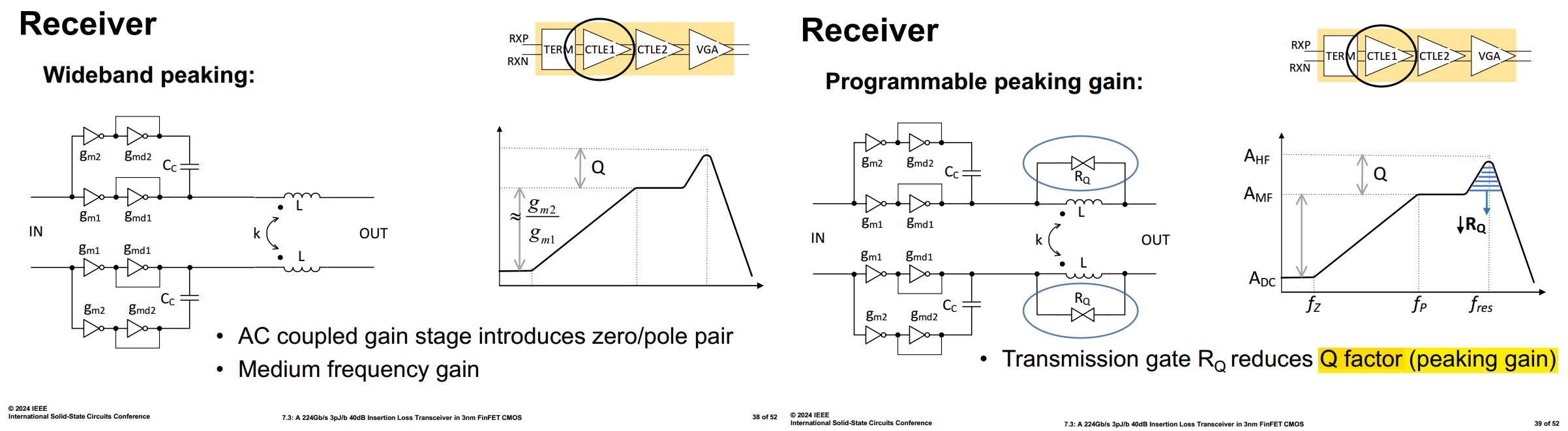
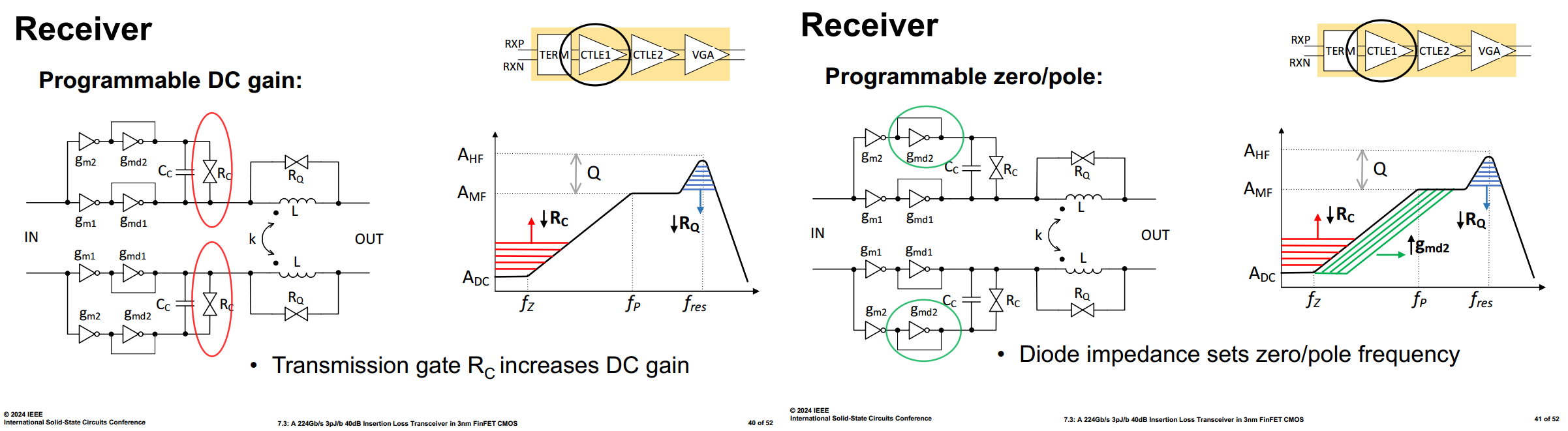
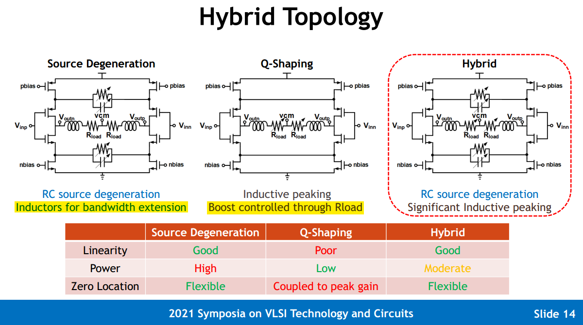
Q-Shaping (LC-tuned Amplifier)
Y. Krupnik et al., "112 Gb/s PAM4 ADC Based SERDES Receiver for Long-Reach Channels in 10nm Process," 2019 Symposium on VLSI Circuits, Kyoto, Japan, 2019, pp. C266-C267, [https://sci-hub.jp/10.23919/VLSIC.2019.8778136]
—, "112-Gb/s PAM4 ADC-Based SERDES Receiver With Resonant AFE for Long-Reach Channels," in IEEE Journal of Solid-State Circuits, vol. 55, no. 4, pp. 1077-1085, April 2020, [https://sci-hub.jp/10.1109/JSSC.2019.2959511]
S. Kiran et al., "A 56GHz Receiver Analog Front End for 224Gb/s PAM-4 SerDes in 10nm CMOS," 2021 Symposium on VLSI Circuits, Kyoto, Japan, 2021, pp. 1-2, [https://sci-hub.jp/10.23919/VLSICircuits52068.2021.9492471]
Y. Segal et al., "A 1.41pJ/b 224Gb/s PAM-4 SerDes Receiver with 31dB Loss Compensation," 2022 IEEE International Solid-State Circuits Conference (ISSCC), San Francisco, CA, USA, 2022, pp. 114-116, [https://sci-hub.jp/10.1109/ISSCC42614.2022.9731794]
A. Khairi et al., "A 1.41-pJ/b 224-Gb/s PAM4 6-bit ADC-Based SerDes Receiver With Hybrid AFE Capable of Supporting Long Reach Channels," in IEEE Journal of Solid-State Circuits, vol. 58, no. 1, pp. 8-18, Jan. 2023, doi: 10.1109/JSSC.2022.3211475
D. Pfaff et al., "A 224 Gb/s 3 pJ/bit 40 dB Insertion Loss Transceiver in 3-nm FinFET CMOS," in IEEE Journal of Solid-State Circuits, vol. 60, no. 1, pp. 9-22, Jan. 2025, doi: 10.1109/JSSC.2024.3466092
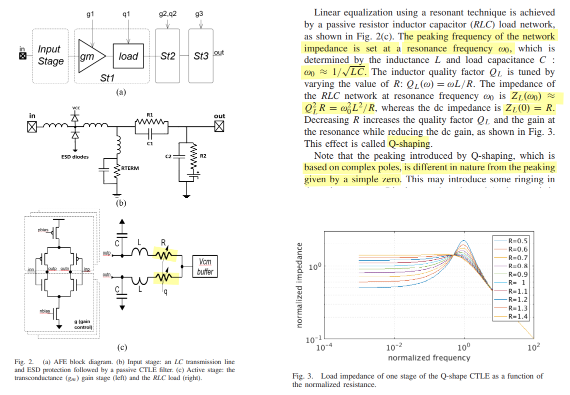
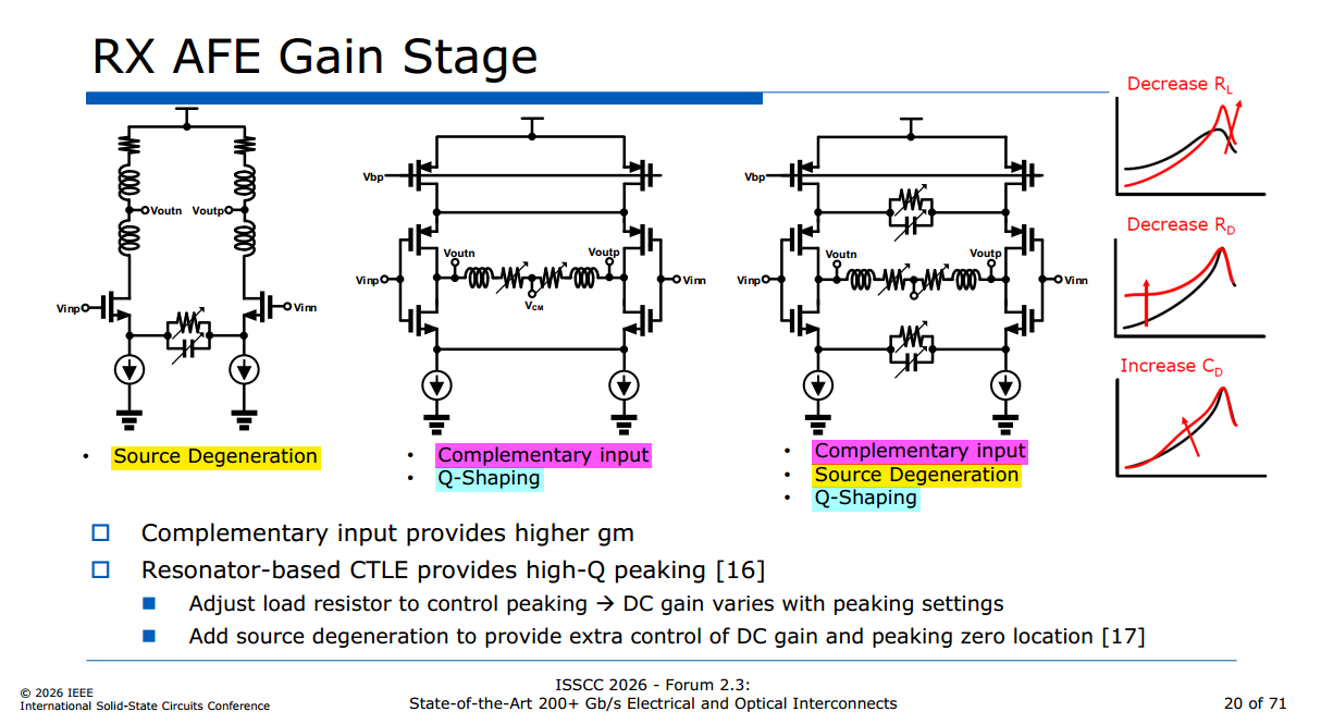
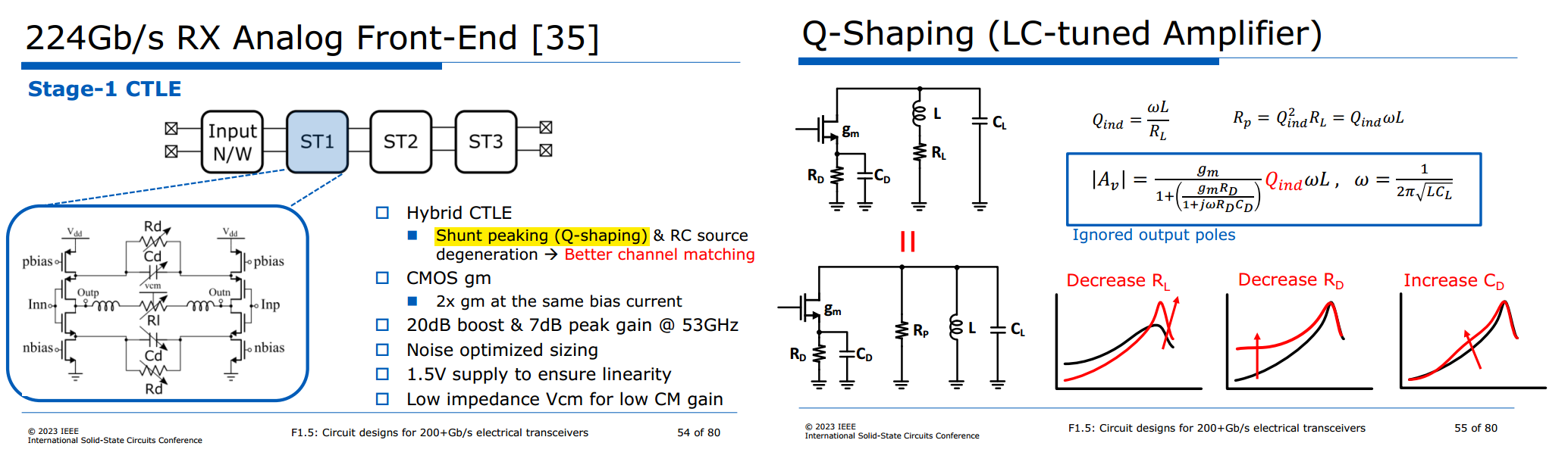
At resonant frequency \[ \boxed{|A_v|= \frac{g_m} {1+\left(\dfrac{g_mR_D}{1+j\omega R_DC_D}\right)} Q_{\mathrm{ind}}\omega L, \qquad \omega=\frac{1}{2\pi\sqrt{L_C L_L}}} \] where \(Q_{\mathrm{ind}}=\frac{\omega L}{R_L}, \qquad R_p=Q_{\mathrm{ind}}^{\,2}R_L=Q_{\mathrm{ind}}\omega L\)
Q-Shaping w/ Parallel RLC
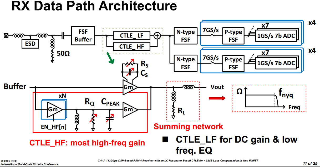
H. Park et al., "7.4 A 112Gb/s DSP-Based PAM-4 Receiver with an LC-Resonator-Based CTLE for >52dB Loss Compensation in 4nm FinFET," 2025 IEEE International Solid-State Circuits Conference (ISSCC), San Francisco, CA, USA, 2025, pp. 142-144, doi: 10.1109/ISSCC49661.2025.10904638.
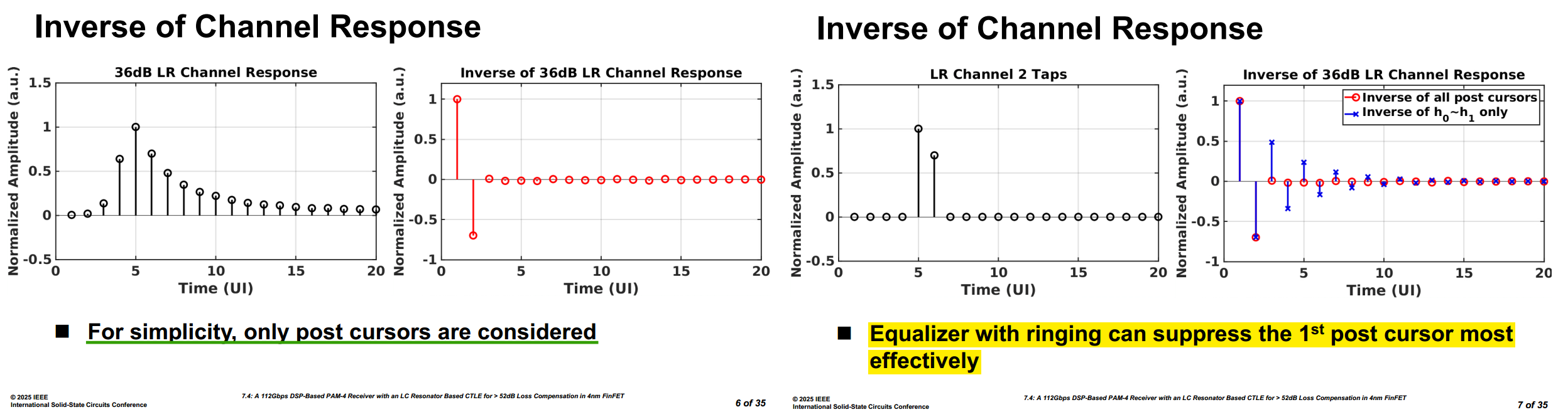
With Zero-Forcing, inverse of \(h_0 \sim h_1\) only
1 | ┌ 1 0 0 0 ┐ ┌c0┐ ┌1┐ |
1 | % Define the coefficient matrix A |
the other method: Treat \(z^{-1}\) as an ordinary variable and divide 1 by \(1+0.7z^{-1}\), working in ascending powers of \(z^{-1}\)
1 | 1 − 0.7z⁻¹ + 0.49z⁻² − 0.343z⁻³ + … ← quotient = c |
Use \(1/(1 − r) = 1 + r + r^2 + \dots\) and \(r=-\alpha z^{-1}\) \[ \boxed{\frac{1}{1+\alpha z^{-1}} = 1 - \alpha z^{-1} + \alpha \left( \alpha z^{-2} - \alpha^2 z^{-3} + \dots \right)} \] that is \[ \frac{1}{1+0.7z^{-1}} = 1 - 0.7z^{-1} + 0.7\left( 0.7 z^{-2} - 0.49 z^{-3} + \dots \right) \]
1 | % Define the coefficient matrix A |
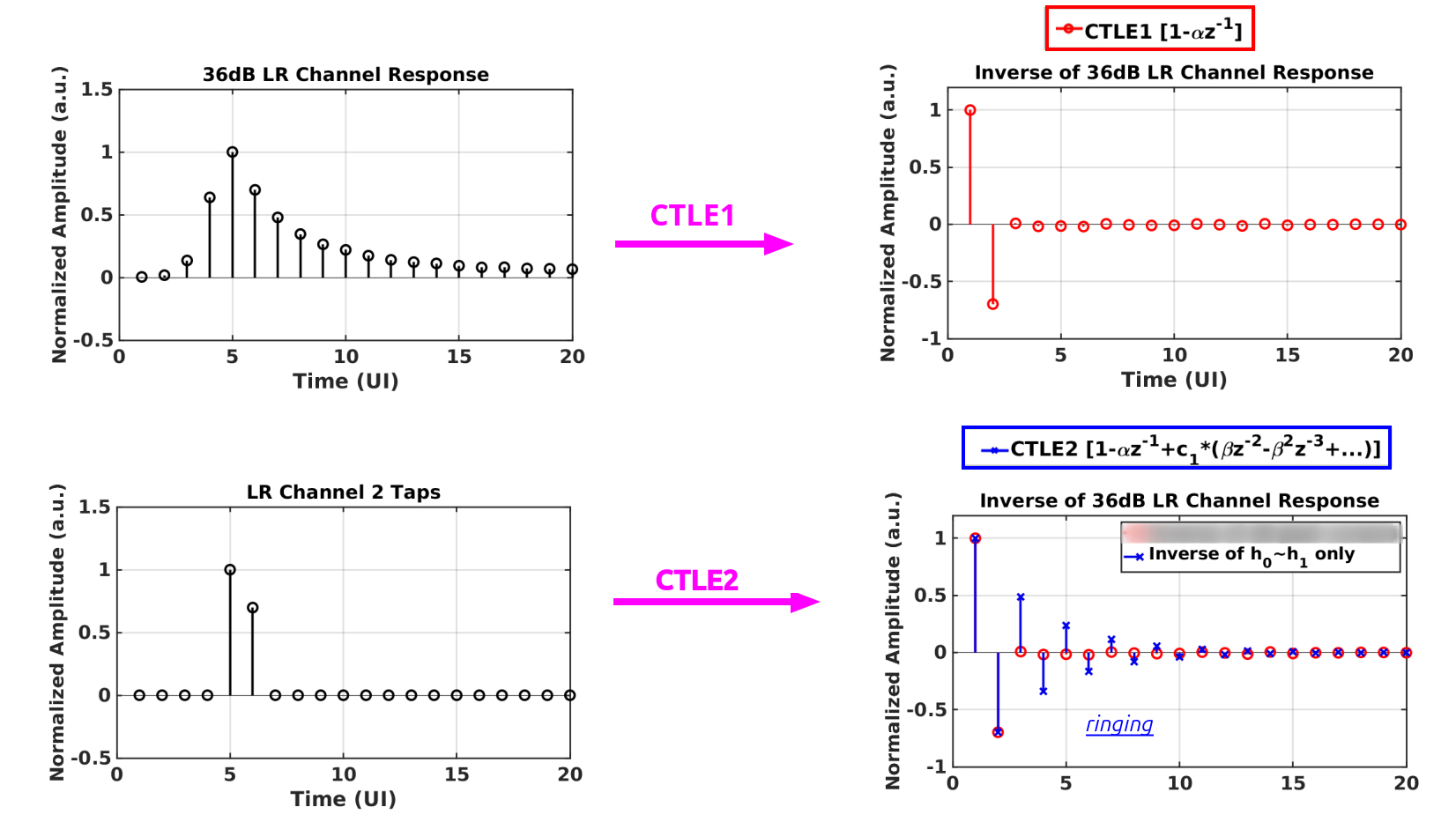
“Inverse of 36 dB LR Channel Response” shows the impulse-response taps of the inverse filter/equalizer.
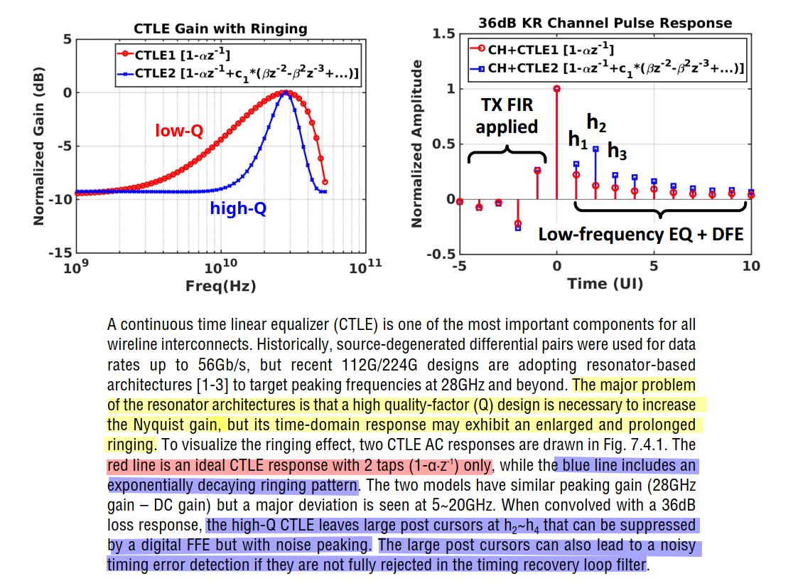
CTLE1: \(1-\alpha z^{-1}\), without pole
CTLE2: \(1-\alpha z^{-1} + c_1 (\beta z^{-2} - \beta^2 z^{-3} + \dots) = 1 - \alpha z^{-1} + \frac{c_1\beta z^{-2}}{1 + \beta z^{-1}}\), with pole \(-\beta\)

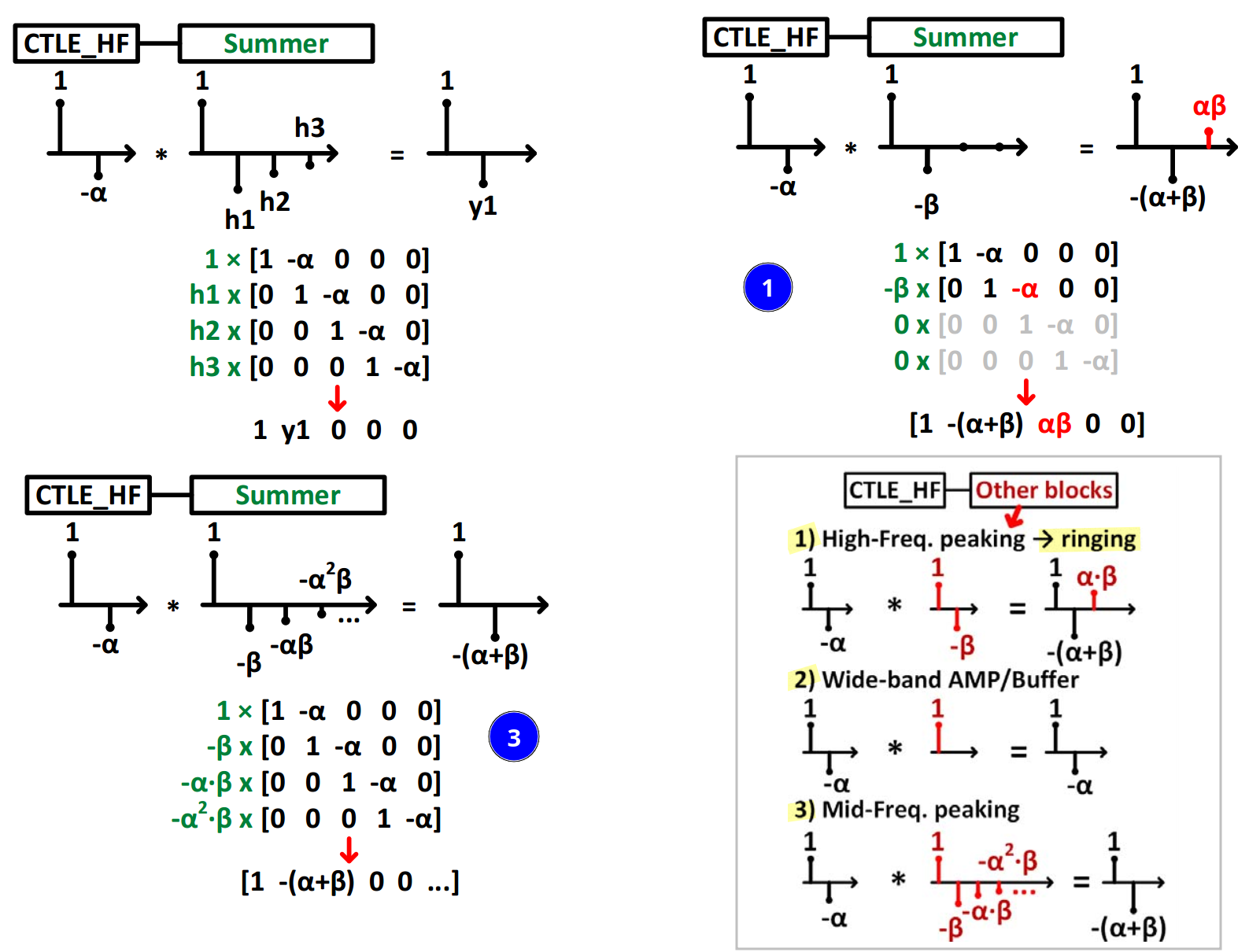
The Summer response is also treated as an impulse-response tap sequence
when the starting sequence is the channel’s pulse response, convolving it with the equalizer’s impulse-response taps gives the equalized pulse-response taps:
\[ p_{\text{out}}[n]=p_{\text{channel}}[n]*h_{\text{EQ}}[n] \]
The distinction is whether the transmitted pulse is already included:
\[ \underbrace{p_{\text{TX}}*h_{\text{channel}}}_{p_{\text{channel}}} *h_{\text{EQ}} =p_{\text{out}} \]
So:
- Pulse response ∗ impulse response → pulse response.
- Impulse response ∗ impulse response → combined impulse response.
If CTLE_HF and Summer are both represented by their block impulse responses, their convolution gives the combined impulse response. Including the transmitted pulse gives the pulse response.
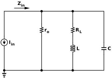
shunt peaking
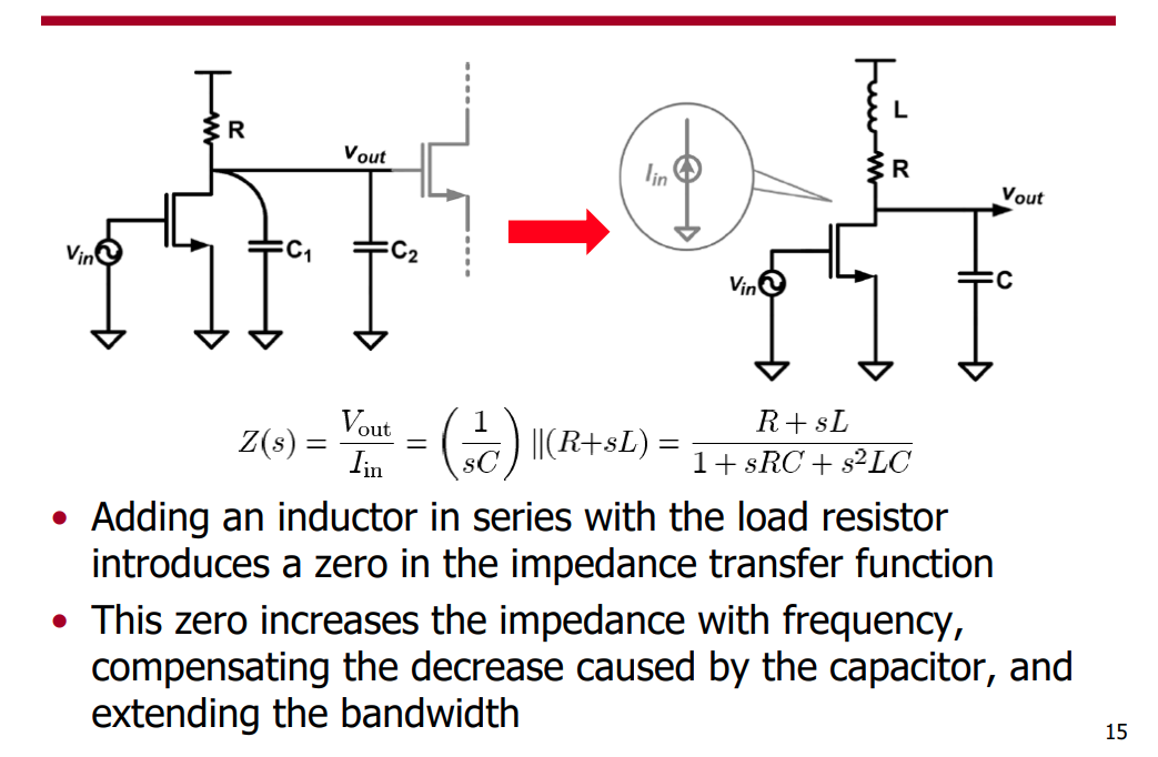
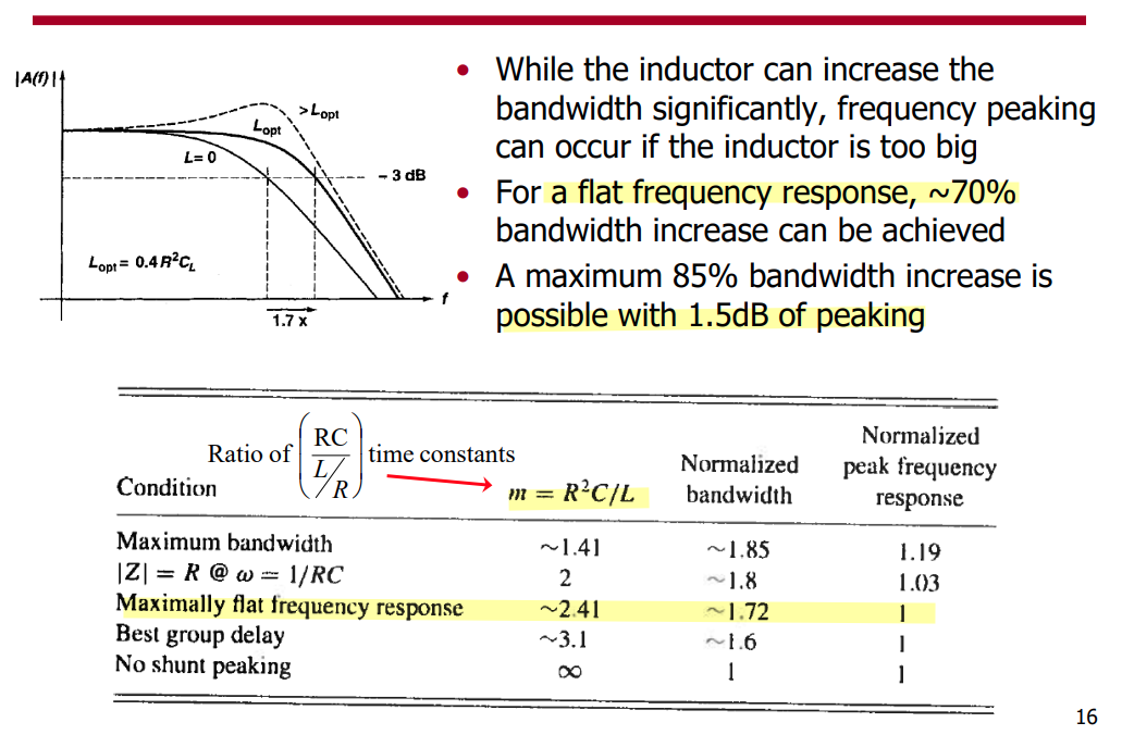
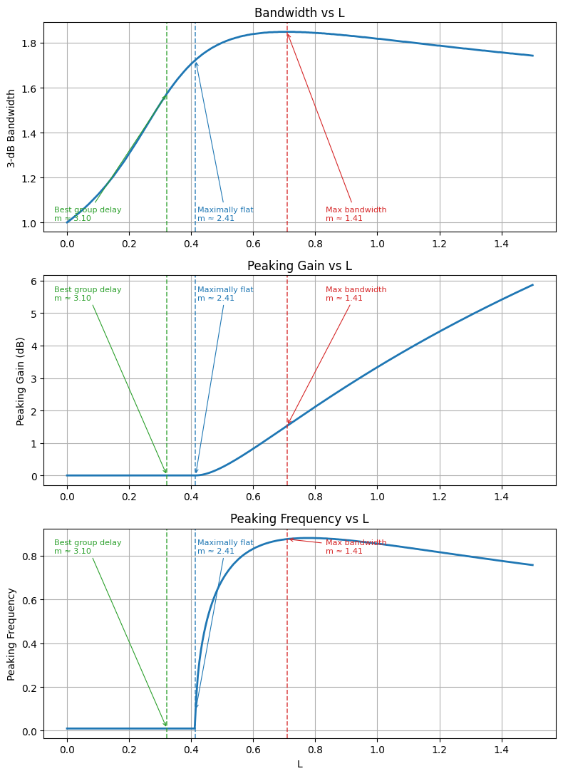
\(\color{red}m=\frac{R^2C}{L}\) is the ratio of the \(R/L\) zero frequency to the original RC pole frequency \(1/RC\), and therefore measures how aggressively the zero compensates the intrinsic RC roll-off.
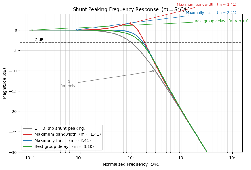
1 | # Normalize R = C = 1 |
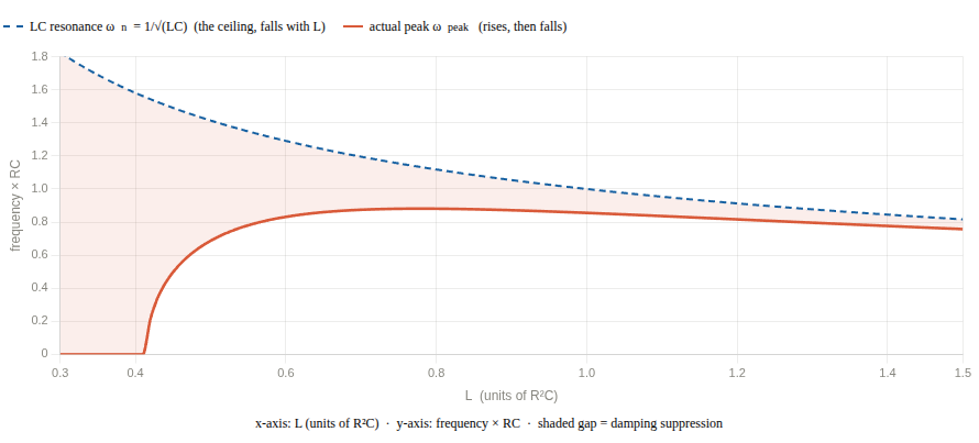
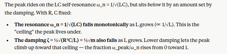
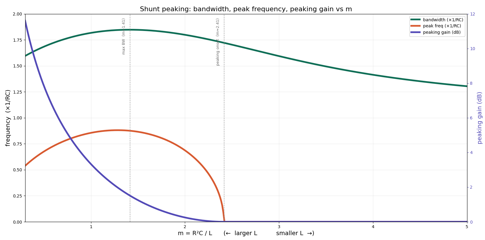
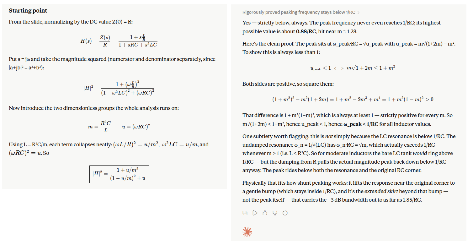
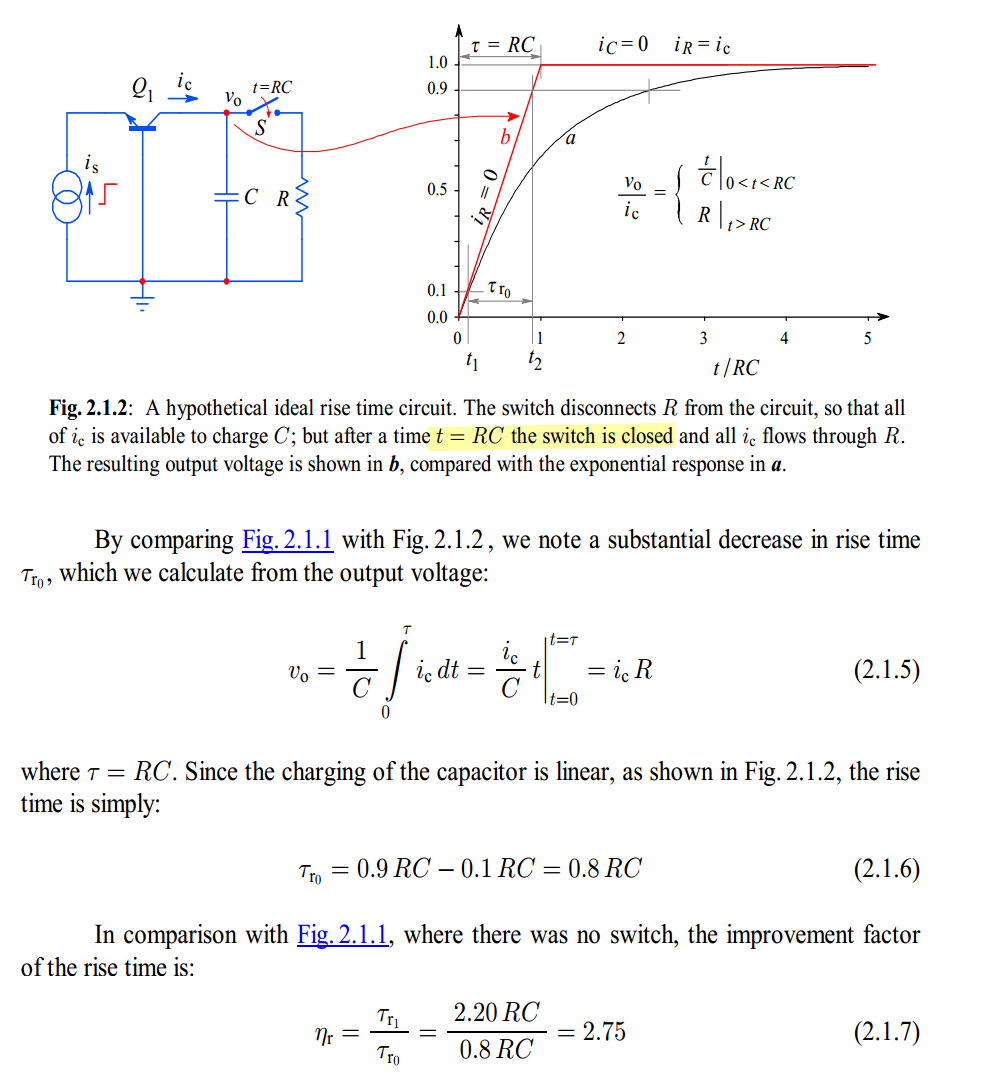
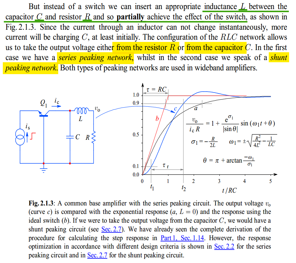
series peaking
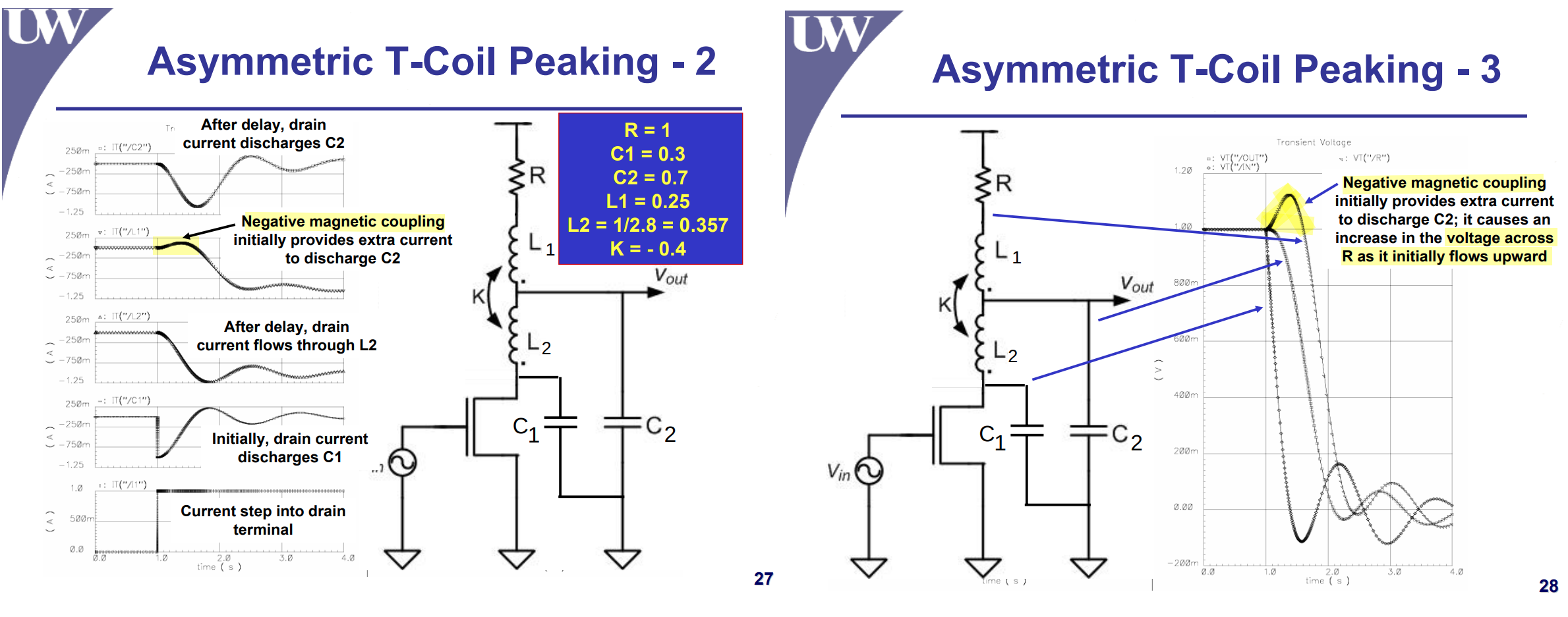
T-Coil Peaking
Jri Lee. ISSCC 2009 Tutorial. CMOS Circuit Techniques for High Speed Wireline Transceivers [http://cc.ee.ntu.edu.tw/~jrilee/course/2009_Tutorial_10.pdf]
CC Chen. Why SerDes Needs a Rule of Thumb for T-Coil Design? [https://youtu.be/RIQLYQG2u0A]
Capacitor Splitting + Magnetic Coupling of a transformer
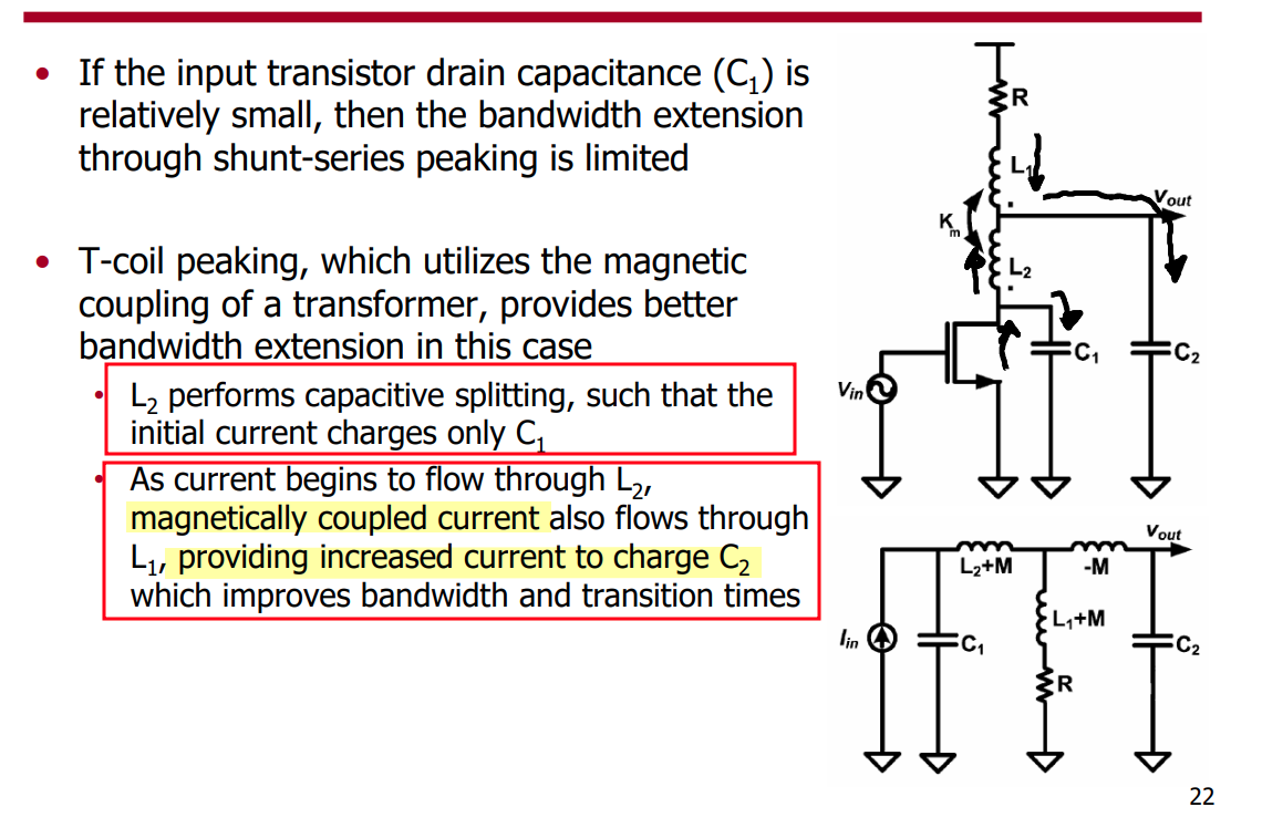

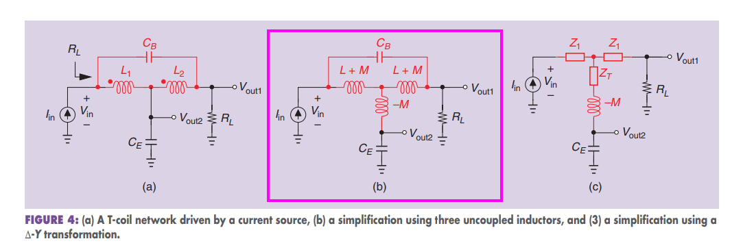
alternative analysis with the below 3 uncoupled inductors model

Three uncoupled inductors model
 \[\begin{align}
V_{P13} &= I_1\cdot sL_1 + I_2\cdot sM = I_1\cdot s(L_1+M) +
(I_1-I_2)\cdot s(-M) \\
V_{P23} &= -I_2\cdot sL_2 - I_1\cdot sM = -I_2\cdot s(L_2 + M) +
(I_1-I_2)\cdot s(-M)
\end{align}\]
\[\begin{align}
V_{P13} &= I_1\cdot sL_1 + I_2\cdot sM = I_1\cdot s(L_1+M) +
(I_1-I_2)\cdot s(-M) \\
V_{P23} &= -I_2\cdot sL_2 - I_1\cdot sM = -I_2\cdot s(L_2 + M) +
(I_1-I_2)\cdot s(-M)
\end{align}\]
The negative inductor \(-M\) can be seen as capacitor \[ -j\omega M = \frac{1}{j}\omega M = \frac{1}{j\omega \frac{1}{\omega^2 M}} \] That is \(C_{-M} = \frac{1}{\omega^2 M} \approx 10 \times C_E\)
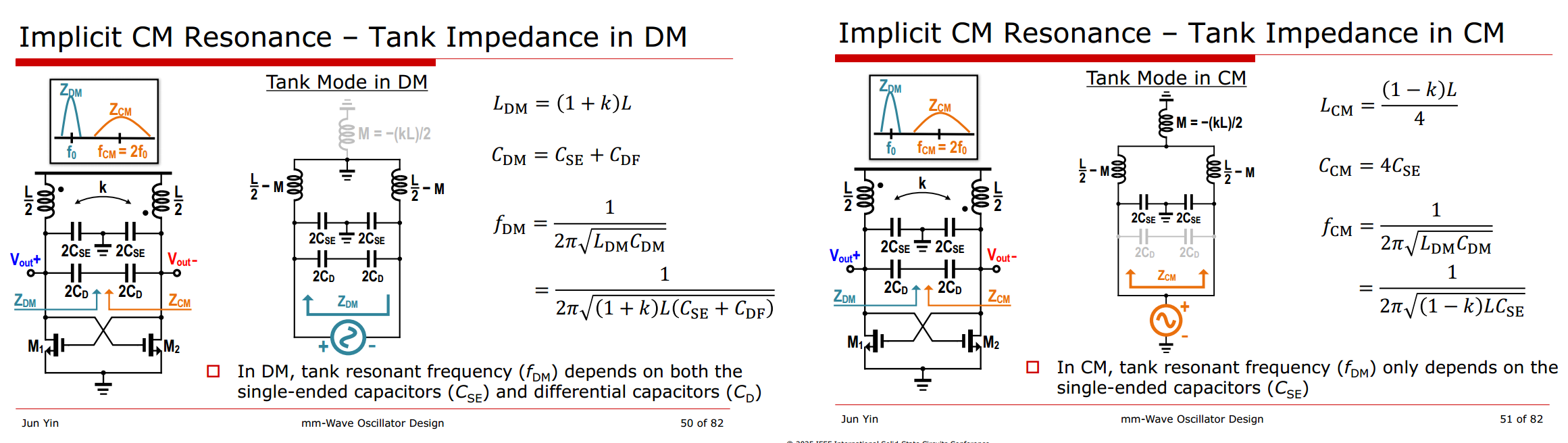
T-coil w/ inverted mutual coupling
J. Kim, J. -K. Kim, B. -J. Lee and D. -K. Jeong, "Design Optimization of On-Chip Inductive Peaking Structures for 0.13- μm CMOS 40-Gb/s Transmitter Circuits," in IEEE Transactions on Circuits and Systems I: Regular Papers, vol. 56, no. 12, pp. 2544-2555, Dec. 2009 [https://sci-hub.st/10.1109/TCSI.2009.2023772]
TODO 📅
Triple Resonance
TODO 📅

series resonance \(\omega_\text{res}\)
Assuming, \(I_\text{in}=\cos\omega_r t\) and \(V_\text{out}=g\cos(\omega_r t +\theta)\)
with \(I_\text{in} = C_L\frac{\mathrm{d}V_\text{out}}{\mathrm{d}t}\), yield \(g=\sqrt{\frac{L}{C}}\) and \(\theta=- \frac{\pi}{2}\), i.e. \(V_\text{out} = \sqrt{\frac{L}{C}}\cos(\omega_r t - \frac{\pi}{2})\)
Active Inductor
B. Razavi, "The Active Inductor [A Circuit for All Seasons]," in IEEE Solid-State Circuits Magazine, vol. 12, no. 2, pp. 7-11, Spring 2020 [https://www.seas.ucla.edu/brweb/papers/Journals/BR_SSCM_2_2020.pdf]
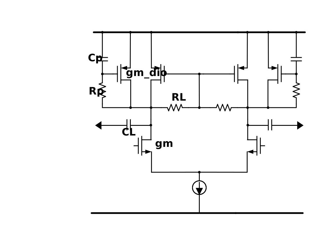
\[\begin{align} A &= \frac{g_mR_L}{1+(g_{\text{m}_{\text{dio}}}+ g_{\text{ds}_\text{tot}})R_L}\cdot \frac{1+R_pC_Ps}{1+\frac{(1+g_{\text{ds}_{\text{tot}}}R_L)R_PC_P+C_PR_L+R_LC_L}{1+(g_{\text{m}_{\text{dio}}}+g_{\text{ds}_\text{tot}})R_L}s + \frac{R_LC_LR_PC_P}{1+(g_{\text{m}_\text{dio}}+g_{\text{ds}_{\text{tot}}})R_L}s^2} \\ &= \frac{g_mR_L}{1+(g_{\text{m}_{\text{dio}}}+ g_{\text{ds}_{\text{tot}}})R_L}\cdot \frac{R_PC_P}{ \frac{R_LC_LR_PC_P}{1+(g_{\text{m}_{\text{dio}}}+g_{\text{ds}_{\text{tot}}})R_L}}\cdot \frac{1/(R_PC_P)+s}{s^2 + \frac{(1+g_{\text{ds}_{\text{tot}}}R_L)R_PC_P+C_PR_L+R_LC_L}{R_PC_P}s + \frac{1+(g_{\text{m}_{\text{dio}}}+g_{\text{ds}_\text{tot}})R_L}{R_LC_LR_PC_P}} \\ &= A_0 \cdot A(s) \end{align}\]
That is
\[\begin{align} \omega_z &= \frac{1}{R_PC_P} \tag{1} \\ \omega_n &= \sqrt{\frac{1+(g_{\text{m}_{\text{dio}}}+ g_{\text{ds}_\text{tot}})R_L}{R_LC_LR_PC_P}} = \sqrt{\omega_{p0}\omega_z} \\ \zeta & = \frac{(1+g_{\text{ds}_\text{tot}}R_L)R_PC_P+C_PR_L+R_LC_L}{R_PC_P} \frac{1}{2 \omega_n} \end{align}\]
Where \[\begin{align} \omega_{p0} &= \frac{1}{(R_L||\frac{1}{g_{\text{m}_{\text{dio}}}}||\frac{1}{g_{\text{m}_{\text{tot}}}})C_L} \tag{2} \end{align}\]
Here, relate \(\omega_{p0}\) and \(\omega_z\) by coefficient \(\alpha\) \[ \omega_{p0} = \alpha \cdot \omega_z \tag{3} \] This way \[ \omega_n= \sqrt{\alpha}\cdot \omega_z \]
\[ \zeta = \frac{1}{2}(K\sqrt{\alpha}+\frac{1+C_P/C_L}{\sqrt{\alpha}}) \tag{4} \]
where \[ K = \frac{R_L||\frac{1}{g_{\text{m}_{\text{dio}}}}||\frac{1}{g_{\text{m}_{\text{tot}}}}}{R_L||g_\text{ds\_tot}} \]
And \(A(s)\) can be expressed as \[ A(s) = \frac{\frac{s}{\omega_z}+1}{\frac{s^2}{\omega_n^2}+2\frac{\zeta}{\omega_n}s+1} \] It magnitude in dB \[ A_\text{dB} = 10\log\frac{1+(\omega/\omega_z)^2}{1+(\omega/\omega_n)^4+2\omega^2(2\zeta^2-1)/\omega_n^2} \] Substitute \(\omega_n\) with Eq (2), followed is obtained \[ A_\text{dB} = 10\log{\frac{\alpha^2(\omega_z^4 + \omega_z^2\omega^2)}{\alpha^2\omega_z^4+\omega^4+2\alpha\omega_z^2(2\zeta^2-1)\omega^2}} \] peaking frequency \[ \omega_\text{peak} = \omega_z\cdot \sqrt{\sqrt{(\alpha+1)^2 - 4\alpha \zeta^2}-1} \] If \(\zeta=1\) \[ \omega_{A_\text{dB = 0dB} } = \sqrt{1-2/\alpha}\cdot \omega_{p0} \qquad \omega_\text{peak} = \omega_z\sqrt{\alpha-2} \qquad A_\text{dB,peak} = 10\log\frac{\alpha^2}{4(\alpha-1)} \]
Negative Capacitance Circuit
Negative Miller Capacitance
S. Gondi and B. Razavi, "Equalization and Clock and Data Recovery Techniques for 10-Gb/s CMOS Serial-Link Receivers," in IEEE Journal of Solid-State Circuits, vol. 42, no. 9, pp. 1999-2011 [pdf]
Sam Palermo. ECEN620 Lecture 14: Limiting Amplifiers (LAs) [https://people.engr.tamu.edu/spalermo/ecen620/lecture14_ee620_limiting_amps.pdf]
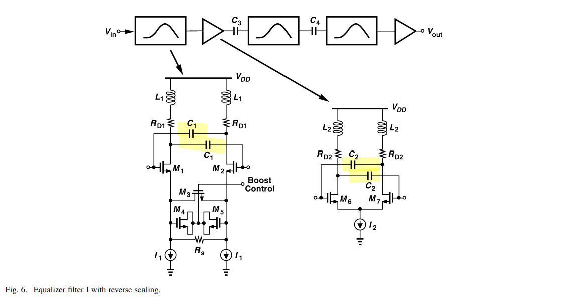
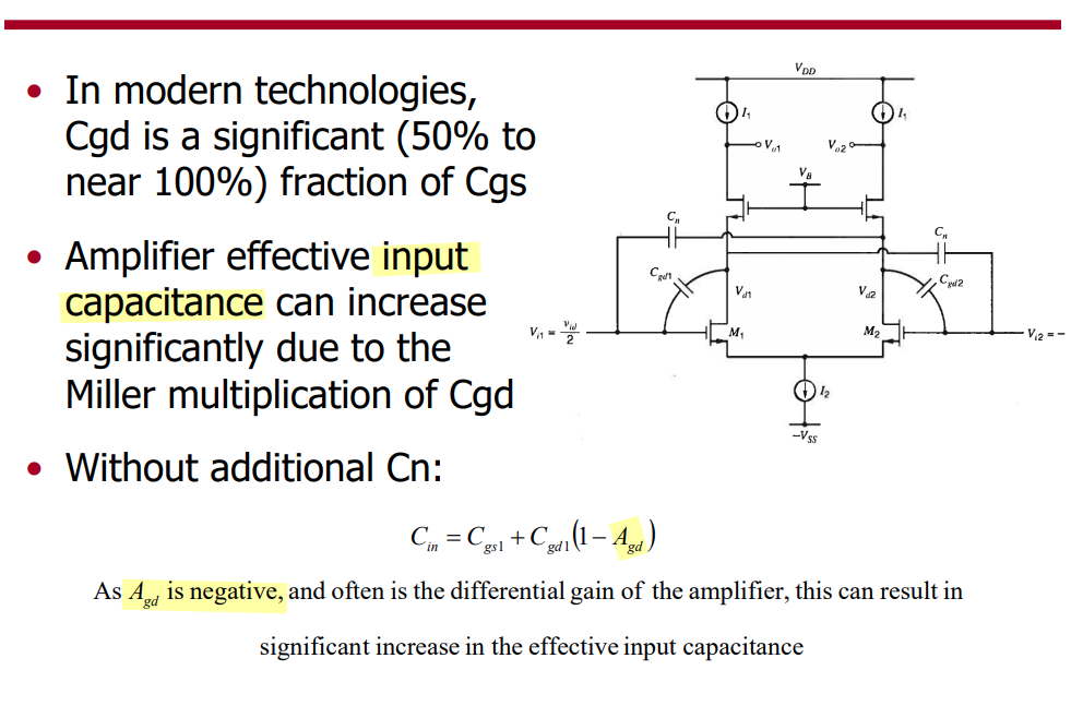 \[
C_{d1} = C_{dd1} + (1+\frac{1}{|A_{gd}|})C_{gd1}
\] where \(A_{gd}\lt 0\)
\[
C_{d1} = C_{dd1} + (1+\frac{1}{|A_{gd}|})C_{gd1}
\] where \(A_{gd}\lt 0\)
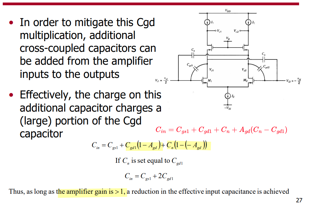
For differential mode input, effective input capacitance \[ C_{in} = C_{gs} +(1+A_{dm}) C_{gd}+\color{red}(1-A_{dm})C_n \] and effective output capacitance \[ C_{out} = C_{dd} + (1+\frac{1}{A_{dm}})C_{gd}+\color{red} (1-\frac{1}{A_{dm}})C_n \] That is \(C_n\) deteriorate the effective output capacitance
For common mode input, effective input capacitance \[ C_{in} = C_{gs} + (1+A_{cm}) C_{gd}+ \color{red}(1+A_{cm})C_n \] and effective output capacitance \[ C_{d1} = C_{dd} + (1+\frac{1}{A_{cm}})C_{gd}+\color{red} (1+\frac{1}{A_{cm}})C_n \] i.e., \(C_n\) deteriorate both effective input capacitance and effective output capacitance, unfortunately
effective input capacitance \(\Pi\) model, which is appropriate for both differential input and common mode input

Suppose \(C_n=C_{gd}\), effective differential input capacitance is same with effective common-mode input capacitance (\(C_n=\frac{A_{dm}-A_{cm}}{A_{dm}+A_{cm}}C_{gd}\))
XCP with Capacitor
B. Razavi, "The Cross-Coupled Pair - Part III [A Circuit for All Seasons]," IEEE Solid-State Circuits Magazine, Issue. 1, pp. 10-13, Winter 2015. [https://www.seas.ucla.edu/brweb/papers/Journals/BR_Magzine3.pdf]
S. Galal and B. Razavi, "10-Gb/s Limiting Amplifier and Laser/Modulator Driver in 0.18um CMOS Technology,” IEEE Journal of Solid-State Circuits, vol. 38, pp. 2138-2146, Dec. 2003.[https://www.seas.ucla.edu/brweb/papers/Journals/G&RDec03_2.pdf]
A. Sheikholeslami, "Bandwidth Extension [Circuit Intuitions]," in IEEE Solid-State Circuits Magazine, vol. 7, no. 2, pp. 8-11, Spring 2015 [https://www.eecg.utoronto.ca/~ali/papers/mag-spr-15-bandwidth-extention.pdf]
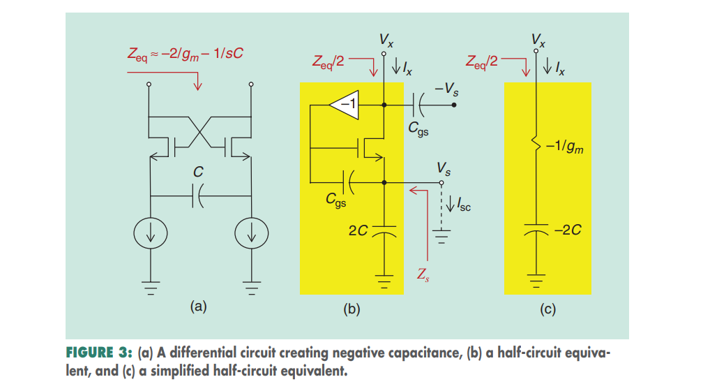
The Cross-Coupled Pair (XCP) can operate as an impedance negator [a.k.a. a negative impedance converter (NIC)]
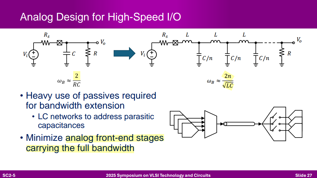
A common application is to create a negative capacitance that can cancel the positive capacitance seen at a port, thereby improving the speed
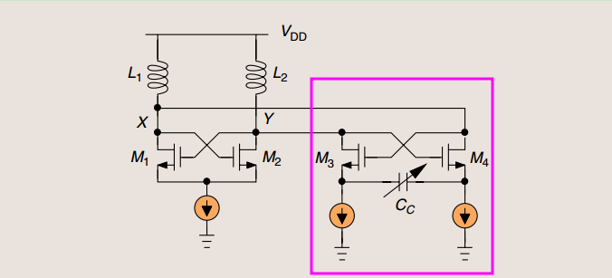 \[
I_{NIC} =\frac{V_{im} - V_{ip}}{\frac{2}{g_m}+\frac{1}{sC_c}} =
\frac{-2V_{ip}}{\frac{2}{g_m}+\frac{1}{sC_c}}
\] Therefore \[
Z_{NIC} = \frac{V_{ip} - V_{im}}{I_{NIC}}=\frac{2V_{ip}}{I_{NIC}} =-
\frac{2}{g_m}-\frac{1}{sC_c}
\] half-circuit
\[
I_{NIC} =\frac{V_{im} - V_{ip}}{\frac{2}{g_m}+\frac{1}{sC_c}} =
\frac{-2V_{ip}}{\frac{2}{g_m}+\frac{1}{sC_c}}
\] Therefore \[
Z_{NIC} = \frac{V_{ip} - V_{im}}{I_{NIC}}=\frac{2V_{ip}}{I_{NIC}} =-
\frac{2}{g_m}-\frac{1}{sC_c}
\] half-circuit
If \(C_{gd}\) is considered, and apply miller effect. half equivalent circuit is shown as below

dual-diode based ESD protection
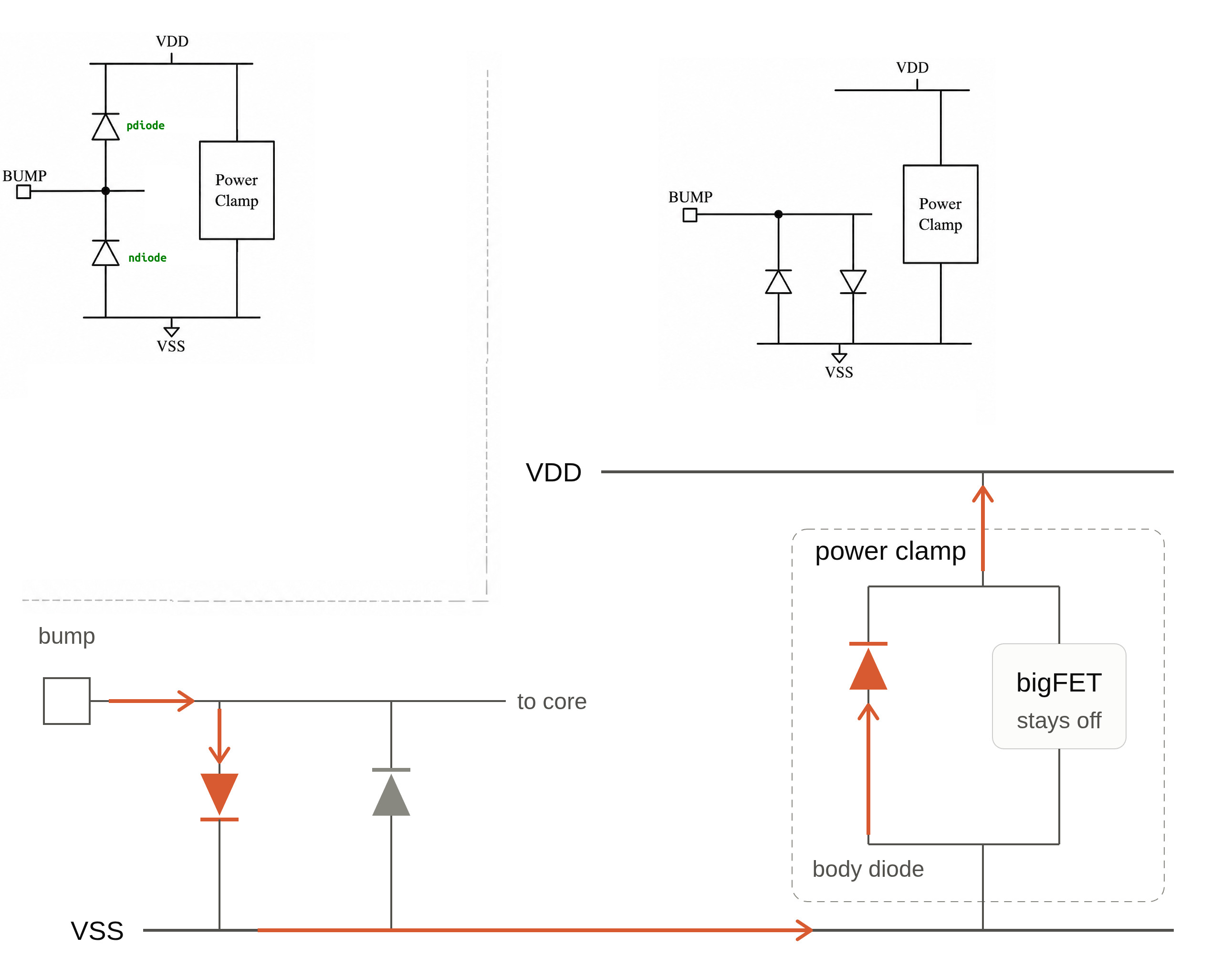
??? which diodes are used in right topology — both pdiode and ndiode are used
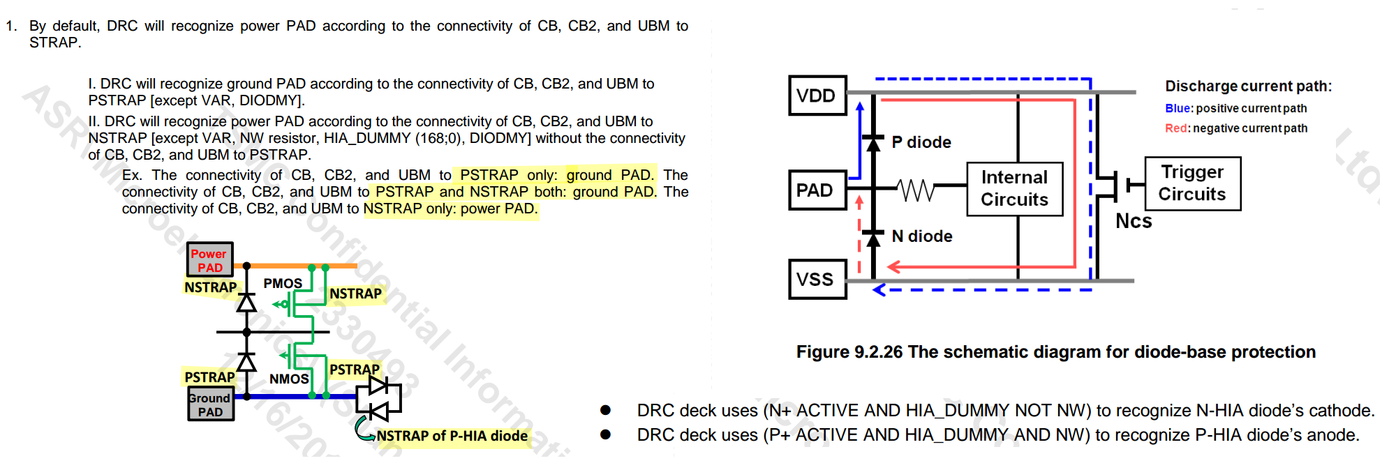
reference
T. Chan Carusone, T. O. Dickson, S. Palermo, S. Shekhar and M. Mansuri, "Modern Wireline Transceivers," in IEEE Journal of Solid-State Circuits, vol. 61, no. 2, pp. 395-422, Feb. 2026 [https://ieeexplore.ieee.org/stamp/stamp.jsp?arnumber=11311714]
Miguel Gandara. CICC2025 Circuits Insights: Wireline Receiver Circuits [https://youtu.be/X4JTuh2Gdzg]
Elad Alon, ISSCC 2014, "T6: Analog Front-End Design for Gb/s Wireline Receivers"
Byungsub Kim, ISSCC 2022, "T11: Basics of Equalization Techniques: Channels, Equalization, and Circuits"
Gain Kim, 2023. Equalization, Architecture, and Circuit Design for High-Speed Serial Link Receiver [www.theise.org/...]
Nhat Nguyen and Masum Hossain, ISSCC 2021 Forum F6.7: 112Gb/s-and-Beyond Long-Reach and Short-Reach Electrical Interfaces
Jihwan Kim, Intel, ISSCC 2023 Forum F1.5: Circuit Designs for 200+Gb/s Electrical Transceivers
Ariel Cohen, Intel, ISSCC 2024 Forum F6.3: Beyond 200Gbps Electrical transceivers – Circuit Architecture, Design Implementation and Silicon Results
Heng Zhang, Broadcom, ISSCC 2025 Forum F4.2: High-speed ADCs for 100Gbps+ Wireline Transceivers
E-Hung Chen, MTK, ISSCC 2026 Forum F2.3: State-of-the-Art 200+ Gb/s Electrical and Optical Interconnects
J. Kim et al., "A 112Gb/s PAM-4 transmitter with 3-Tap FFE in 10nm CMOS," 2018 IEEE International Solid-State Circuits Conference - (ISSCC), San Francisco, CA, USA, 2018 [paper]
S. Shekhar, J. S. Walling and D. J. Allstot, "Bandwidth Extension Techniques for CMOS Amplifiers," in IEEE Journal of Solid-State Circuits, vol. 41, no. 11, pp. 2424-2439, Nov. 2006 [pdf]
David J. Allstot Bandwidth Extension Techniques for CMOS Amplifiers [https://ewh.ieee.org/r5/denver/sscs/Presentations/2007_08_Allstot.pdf]
S. S. Mohan, M. D. M. Hershenson, S. P. Boyd and T. H. Lee, "Bandwidth extension in CMOS with optimized on-chip inductors," in IEEE Journal of Solid-State Circuits, vol. 35, no. 3, pp. 346-355, March 2000 [http://smirc.stanford.edu/papers/JSSC00MAR-mohan.pdf]
J. Paramesh and D. J. Allstot, "Analysis of the Bridged T-Coil Circuit Using the Extra-Element Theorem," in IEEE Transactions on Circuits and Systems II: Express Briefs, vol. 53, no. 12, pp. 1408-1412, Dec. 2006 [https://sci-hub.st/10.1109/TCSII.2006.885971]
S. C. D. Roy, "Comments on "Analysis of the Bridged T-coil Circuit Using the Extra-Element Theorem," in IEEE Transactions on Circuits and Systems II: Express Briefs, vol. 54, no. 8, pp. 673-674, Aug. 2007 [https://sci-hub.st/10.1109/TCSII.2007.899834]
B. Razavi, "The Bridged T-Coil [A Circuit for All Seasons]," IEEE Solid-State Circuits Magazine, Volume. 7, Issue. 40, pp. 10-13, Fall 2015 [https://www.seas.ucla.edu/brweb/papers/Journals/BRFall15TCoil.pdf]
—, "The Design of Broadband I/O Circuits [The Analog Mind]," IEEE Solid-State Circuits Magazine, Volume. 13, Issue. 2, pp. 6-15, Spring 2021 [http://www.seas.ucla.edu/brweb/papers/Journals/BR_SSCM_2_2021.pdf]
Deog-Kyoon Jeong. Topics in IC Design: T-Coil [pdf]
P. Heydari, "Neutralization Techniques for High-Frequency Amplifiers: An Overview," in IEEE Solid-State Circuits Magazine, vol. 9, no. 4, pp. 82-89, Fall 2017 [https://sci-hub.ru/10.1109/MSSC.2017.2745858]
—, "Evolution of Broadband Amplifier Design: From Single-Stage to Distributed Topology," in IEEE Microwave Magazine, vol. 24, no. 9, pp. 18-29, Sept. 2023
Cowan G. Mixed-Signal CMOS for Wireline Communication: Transistor-Level and System-Level Design Considerations. Cambridge University Press; 2024
Starič, Peter and Erik Margan. Wideband amplifiers. (2006) [pdf]
Bob Ross. IBIS Summit [T-Coils and Bridged-T Networks], [T-Coil Topics]
Walling, Jeffrey & Shekhar, Sudip & Allstot, David. (2008). Wideband CMOS Amplifier Design: Time-Domain Considerations. Circuits and Systems I: Regular Papers, IEEE Transactions on. 55. 1781 - 1793. [pdf]
A. A. Abidi, "The T-Coil Circuit Demystified," in IEEE Transactions on Circuits and Systems I: Regular Papers, vol. 72, no. 9, pp. 4469-4480, Sept. 2025
S. Lin, D. Huang and S. Wong, "Pi Coil: A New Element for Bandwidth Extension," in IEEE Transactions on Circuits and Systems II: Express Briefs, vol. 56, no. 6, pp. 454-458, June 2009
M. Kossel et al., "A T-Coil-Enhanced 8.5 Gb/s High-Swing SST Transmitter in 65 nm Bulk CMOS With <−16 dB Return Loss Over 10 GHz Bandwidth," in IEEE Journal of Solid-State Circuits, vol. 43, no. 12, pp. 2905-2920, Dec. 2008 [https://web.mit.edu/magic/Public/papers/04684644.pdf]
S. Galal and B. Razavi, "Broadband ESD protection circuits in CMOS technology," in IEEE Journal of Solid-State Circuits, vol. 38, no. 12, pp. 2334-2340, Dec. 2003, [https://sci-hub.jp/10.1109/JSSC.2003.818568]
M. Ker and Y. Hsiao, "On-Chip ESD Protection Strategies for RF Circuits in CMOS Technology," 2006 8th International Conference on Solid-State and Integrated Circuit Technology Proceedings, 2006, pp. 1680-1683 [https://sci-hub.jp/10.1109/ICSICT.2006.306371]
M. Ker, C. Lin and Y. Hsiao, "Overview on ESD Protection Designs of Low-Parasitic Capacitance for RF ICs in CMOS Technologies," in IEEE Transactions on Device and Materials Reliability, vol. 11, no. 2, pp. 207-218, June 2011 [https://sci-hub.jp/10.1109/TDMR.2011.2106129]
Kosnac, Stefan (2021) Analysis of On-Chip Inductors and Arithmetic Circuits in the Context of High Performance Computing [https://archiv.ub.uni-heidelberg.de/volltextserver/30559/1/Dissertation_Stefan_Kosnac.pdf]
Chapter 4.5. High Frequency Passive Devices [https://www.cambridge.org/il/files/7713/6698/2369/HFIC_chapter_4_passives.pdf]
K. Yadav, P. -H. Hsieh and A. Chan Carusone, "Linearity Analysis of Source-Degenerated Differential Pairs for Wireline Applications," in IEEE Open Journal of Circuits and Systems [https://ieeexplore.ieee.org/stamp/stamp.jsp?tp=&arnumber=10769573]
Minsoo Choi et al., "An Approximate Closed-Form Channel Model for Diverse Interconnect Applications," IEEE Transactions on Circuits and Systems-I: Regular Papers, vol. 61, no. 10, pp. 3034-3043, Oct. 2014. [https://sci-hub.jp/10.1109/TCSI.2014.2327275]