Wireline Transmitter
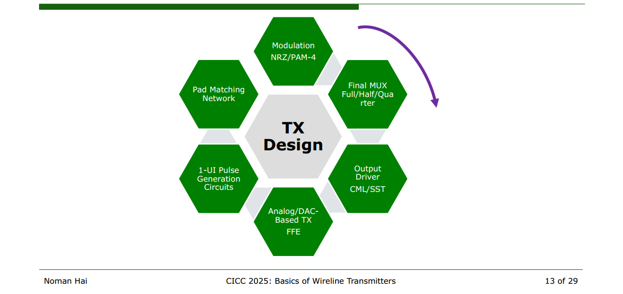
Analog-based TX vs. DSP/DAC TX
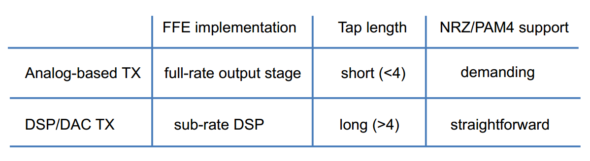
SST vs. CML Driver
Z. Toprak-Deniz et al., "A 128-Gb/s 1.3-pJ/b PAM-4 Transmitter With Reconfigurable 3-Tap FFE in 14-nm CMOS," in IEEE Journal of Solid-State Circuits, vol. 55, no. 1, pp. 19-26, Jan. 2020 [https://sci-hub.st/10.1109/JSSC.2019.2939081]
Design Challenges Of High-Speed Wireline Transmitters [https://semiengineering.com/design-challenges-of-high-speed-wireline-transmitters/]
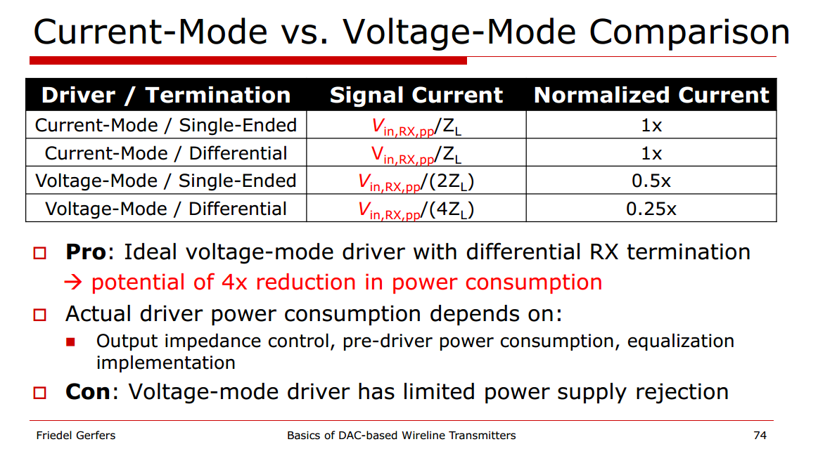
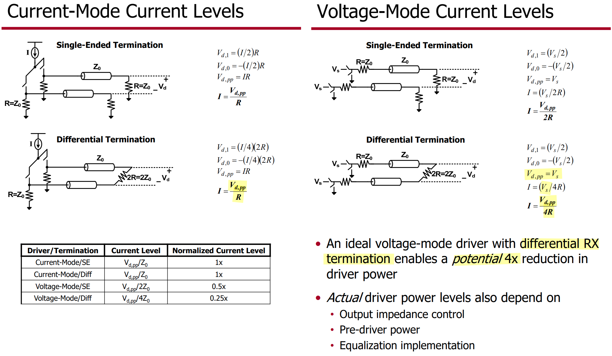
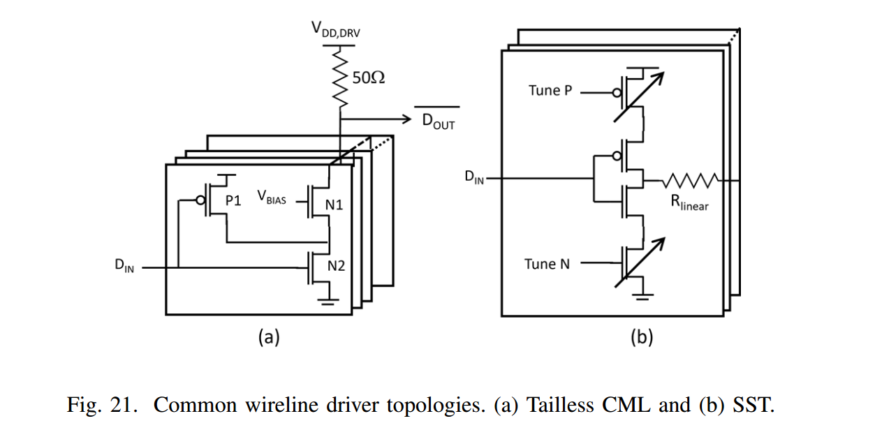
The source-series terminated (SST) drivers are more power-efficient than their current mode logic (CML) counterparts due to their lower termination power
differential output amplitude
\[ V_{ad,SST} = \frac{V_{DD}}{4R_T}\cdot 2R_T = \boxed{I_{DD}\cdot 2R_T} \qquad V_{ad,CML} = \frac{I_{DD}}{4}\cdot 2R_T = \boxed{\frac{1}{4} I_{DD}\cdot 2R_T} \]
To achieve the same differential output amplitude, CML topologies consume \(4\) times the current of SST topologies
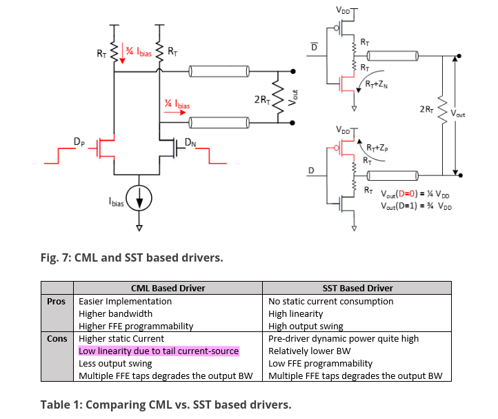
Current mode drivers become power competitive at very high data rates
- Dynamic power consumption scales with frequency \(\Longrightarrow\) SST drivers lose power advantage
Serialization Approaches
Z. Toprak-Deniz et al., "A 128-Gb/s 1.3-pJ/b PAM-4 Transmitter With Reconfigurable 3-Tap FFE in 14-nm CMOS," in IEEE Journal of Solid-State Circuits, vol. 55, no. 1, pp. 19-26, Jan. 2020 [https://sci-hub.st/10.1109/JSSC.2019.2939081]
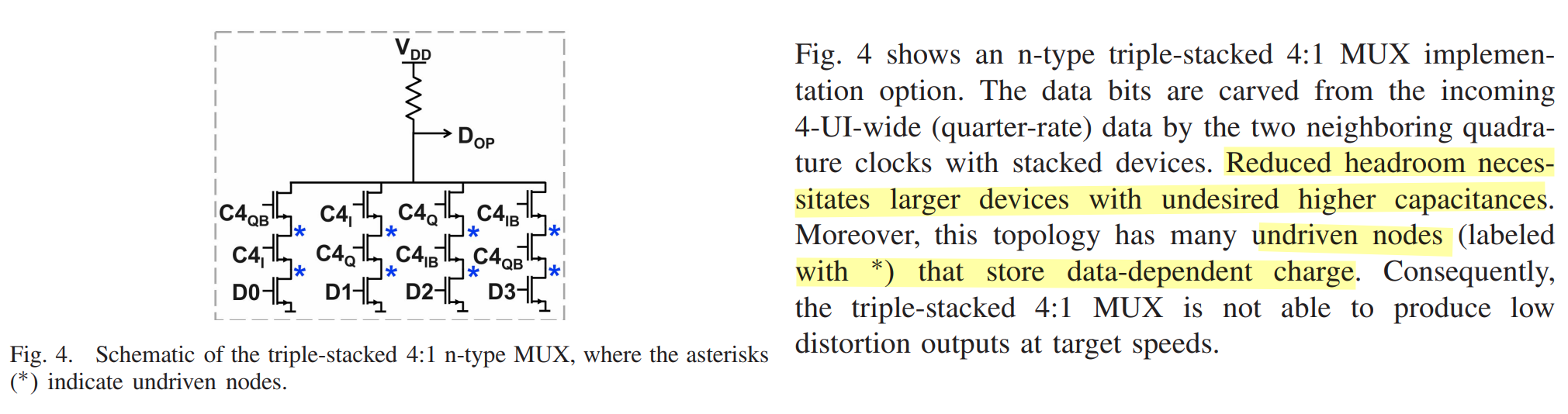
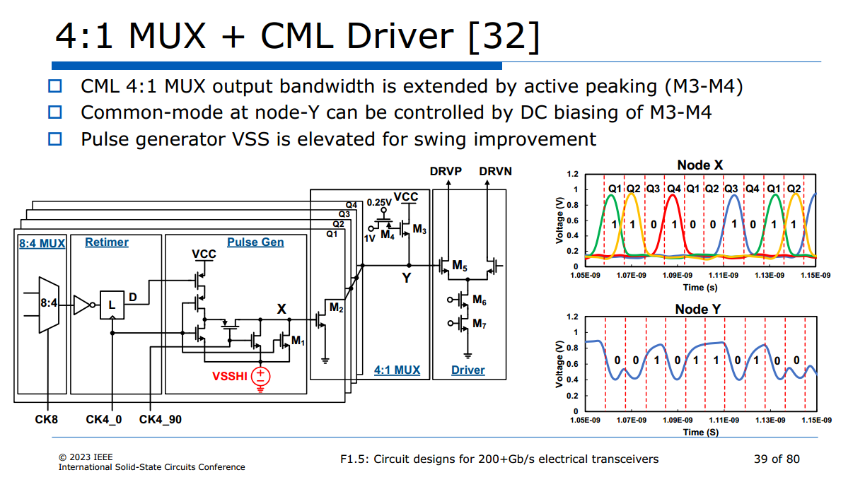
triple-stacked 4:1 n-type MUX

2-1 mux timing

The circuit alone does not fix the bit order. It depends on which clock edge arrives first:
- First edge rising: the a-flop captures first, and the output is a₀, b₀, a₁, b₁, …
- First edge falling: the b-flop captures first, and the output is b₀, a₀, b₁, a₁, …

The inverter chain sets the hold margin at the mux
The first two inverters delay the flop clocks behind the select, so each flop updates only after the mux has switched away from it
The third inverter mainly provides the inverted clock for the b-flop, and it adds a little extra hold margin to that path
Because t_su + t_hd ≈ T/2, every bit of delay added for hold comes out of setup. The chain should therefore be just long enough to guarantee positive hold margin across PVT.
divider latch timing

The clk_d inverters set where the latch's transparent window sits inside di's stable window:
- d_div is the delay from the clk edge to di changing: t_inv + t_cq,FF + t_mux,sel.
- d_c is the delay of the clk_d path: 2·t_inv, plus the latch's internal delay.
From those:
t_hd ≈ d_div − d_c t_su ≈ T/2 +d_c − d_div
The sum is fixed at T/2, so adding clk_d delay buys setup by spending hold, and removing it does the reverse. The window is centred (t_su = t_hd = T/4) when d_c ≈ d_div − T/4
Two latches

1-UI Data Stagger
C. Menolfi et al., "6.2 A 112Gb/S 2.6pJ/b 8-Tap FFE PAM-4 SST TX in 14nm CMOS," 2018 IEEE International Solid-State Circuits Conference - (ISSCC), San Francisco, CA, USA, 2018, pp. 104-106 [https://sci-hub.ru/10.1109/ISSCC.2018.8310205]
Z. Toprak-Deniz et al., "6.6 A 128Gb/s 1.3pJ/b PAM-4 Transmitter with Reconfigurable 3-Tap FFE in 14nm CMOS," 2019 IEEE International Solid-State Circuits Conference - (ISSCC), San Francisco, CA, USA, 2019, pp. 122-124 [https://sci-hub.ru/10.1109/ISSCC.2019.8662479]
—, "A 128-Gb/s 1.3-pJ/b PAM-4 Transmitter With Reconfigurable 3-Tap FFE in 14-nm CMOS," in IEEE Journal of Solid-State Circuits, vol. 55, no. 1, pp. 19-26, Jan. 2020 [https://sci-hub.ru/10.1109/JSSC.2019.2939081]
T. O. Dickson et al., "C3.2 A 72GS/s, 8-bit DAC-based Wireline Transmitter in 4nm FinFET CMOS for 200+Gb/s Serial Links," 2022 IEEE Symposium on VLSI Technology and Circuits (VLSI Technology and Circuits), Honolulu, HI, USA, 2022, pp. 28-29 [https://sci-hub.ru/10.1109/VLSITechnologyandCir46769.2022.9830421]
—, "A 72-GS/s, 8-Bit DAC-Based Wireline Transmitter in 4-nm FinFET CMOS for 200+ Gb/s Serial Links," in IEEE Journal of Solid-State Circuits, vol. 58, no. 4, pp. 1074-1086, April 2023, doi: 10.1109/JSSC.2022.3228632
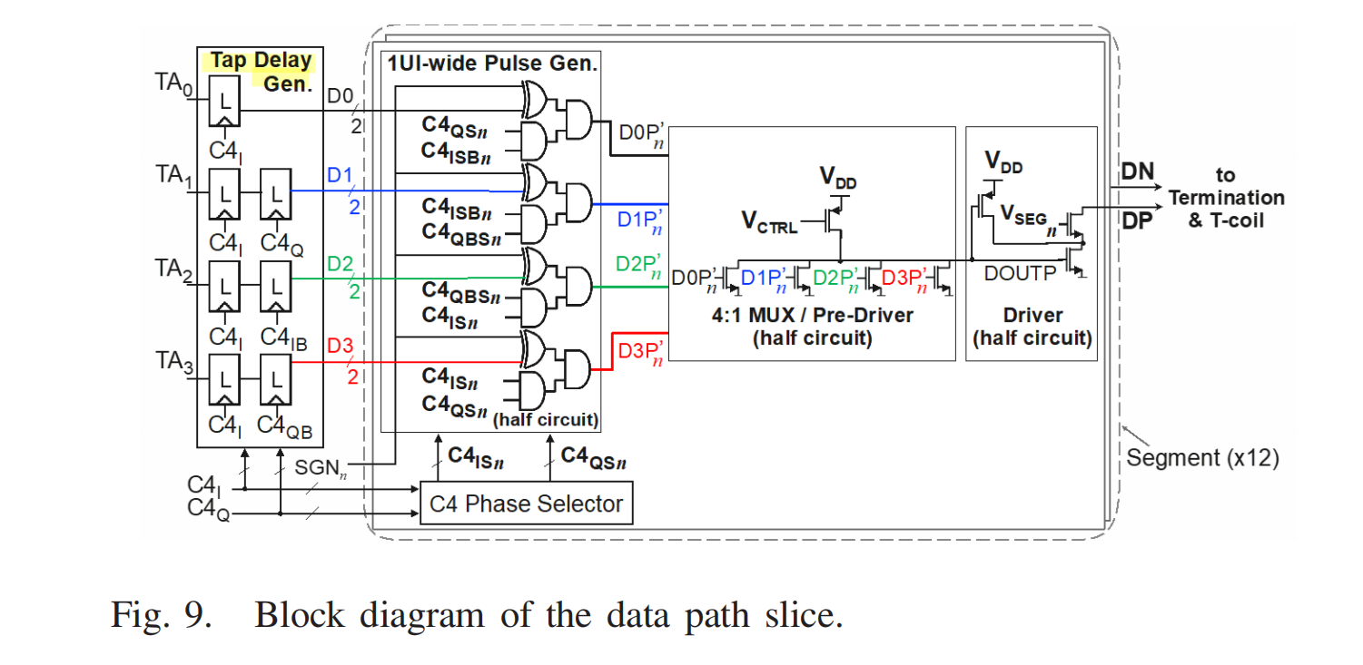
a.k.a Phase Aligner, Tap Delay Generator
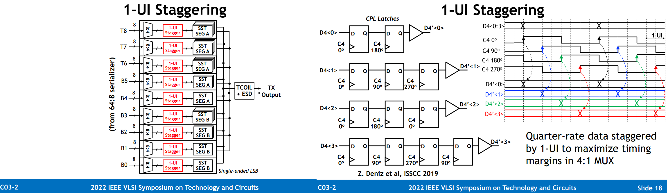

D4'<0> is launched by the C4 0° rising edge, <1> by 90°, <2> by 180° and <3> by 270°
Why the chains have 2, 3, 3 and 4 latches:
- each latch passes data on to the next latch to open. That hop can only be 1 UI (a 90° step) or 2 UI (a 180° step)
- the first 0° latch opens at 2 UI,
and the outputs must launch at 4, 5, 6 and 7 UI.
- one hop for <0> (+2)
- two for <1> (+1 +2)
- two for <2> (+2 +2)
- three for <3> (+1 +2 +2)
These match the slide's chains, which are the shortest possible for those targets
The two hop types also have different margins, which ties back to the earlier figures:
- 90° hop: the input changes in the middle of the next latch's hold phase, so setup and hold are both about 1 UI.
- 180° hop: this is the master–slave case. The input changes right after the next latch closes, so hold margin is only clock-to-Q, while setup gets 2 UI
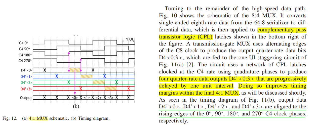
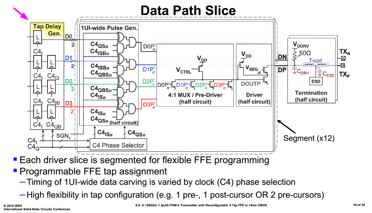
a tap delay generator retime the incoming data and provide 1-UI-staggered quarter-rate data (D0-D3)
.drawio.svg)
Fig 9. works for D0–D2, but the D3 path races. So Fig. 9 is probably simplified
Fix: add one C4_Q latch to the D3 path, giving C4_I → C4_Q → C4_QB.
.drawio.svg)
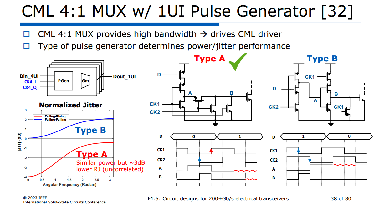
1-UI Clock Pulse Generator
J. Kim et al., “A 224Gb/s DAC-Based PAM-4 Transmitter with 8-Tap FFE in 10nm CMOS,” ISSCC 2021 [https://sci-hub.jp/10.1109/ISSCC42613.2021.9365840]
duty correction & delay adjustment
TODO 📅
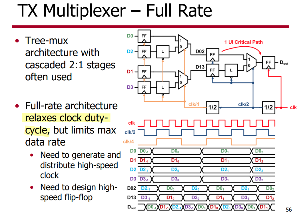
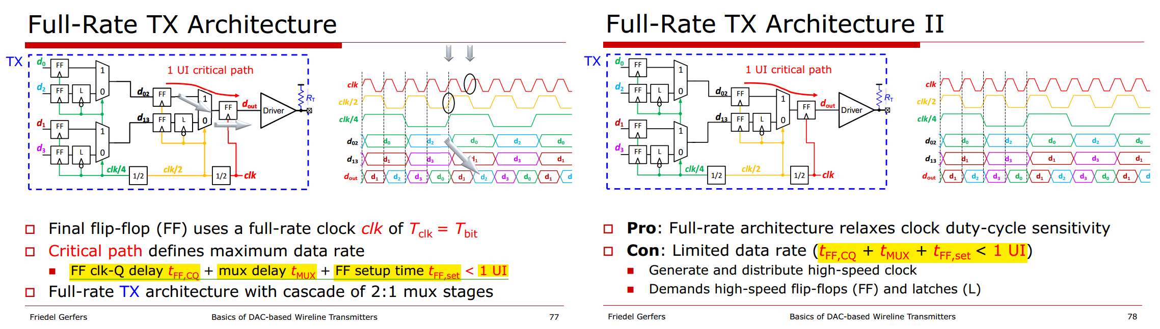
Full-rate TX architecture
Sam Palermo, ECEN720: High-Speed Links Circuits and Systems Spring 2025 Lecture 5: Termination, TX Driver, & Multiplexer Circuits [https://people.engr.tamu.edu/spalermo/ecen689/lecture5_ee720_termination_txdriver.pdf]
J. Cao et al., "OC-192 transmitter and receiver in standard 0.18-/spl mu/m CMOS," in IEEE Journal of Solid-State Circuits, vol. 37, no. 12, pp. 1768-1780, Dec. 2002 [https://sci-hub.jp/10.1109/JSSC.2002.804336]
With the FFs, latches, and clocks unchanged, reversing the MUX selection still works, but adds latency
The bit order is preserved; each bit is selected later.
- Reversing both first-stage MUXes adds 2 UI
- Reversing the final MUX adds 1 UI.
- Reversing all three preserves (D_0,D_1,D_2,D_3,), with 3 UI additional latency
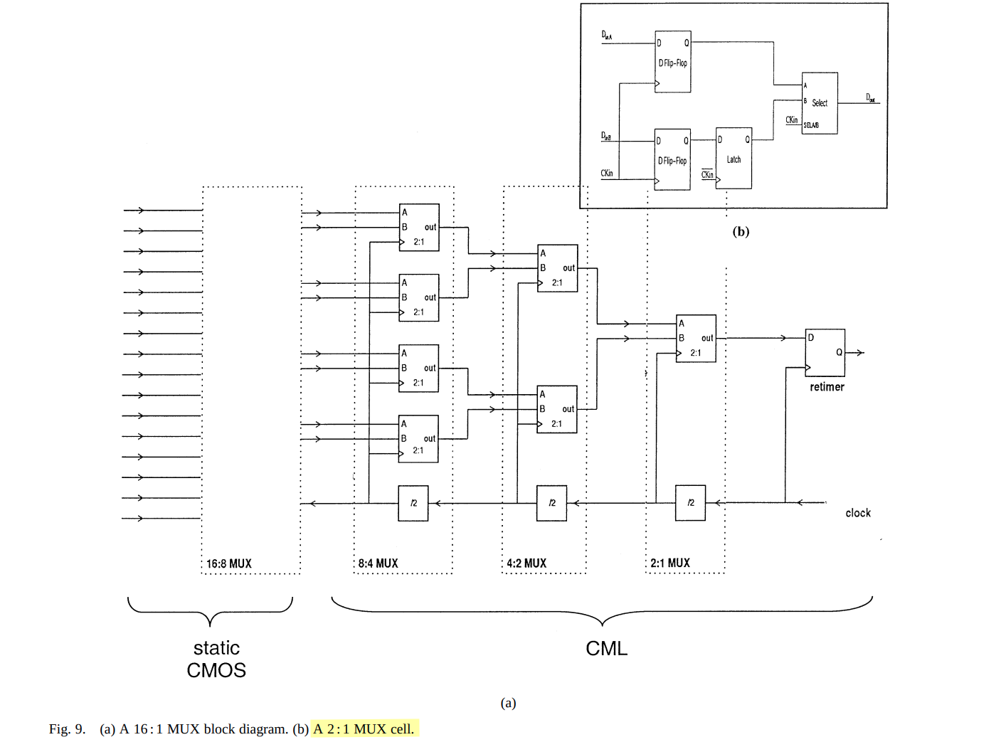
The retimer between the final stage of the MUX and the output driver is used to reduce the data jitter due to the bandwidth limitation of the selection circuit in the 2 : 1 MUX cell and duty cycle distortion of the half-rate clock driving that stage
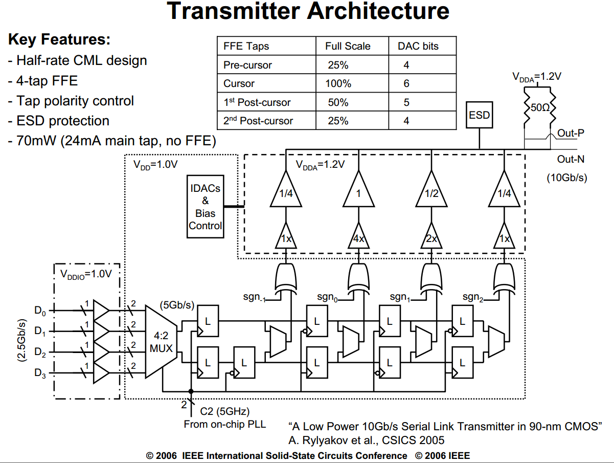
Half-rate TX architecture
M. Meghelli et al., "A 10Gb/s 5-Tap-DFE/4-Tap-FFE Transceiver in 90nm CMOS," 2006 IEEE International Solid State Circuits Conference - Digest of Technical Papers, San Francisco, CA, USA, 2006, pp. 213-222 [https://sci-hub.ru/10.1109/ISSCC.2006.1696051]
J. F. Bulzacchelli et al., "A 10-Gb/s 5-Tap DFE/4-Tap FFE Transceiver in 90-nm CMOS Technology," in IEEE Journal of Solid-State Circuits, vol. 41, no. 12, pp. 2885-2900, Dec. 2006 [https://sci-hub.ru/10.1109/JSSC.2006.884342]
Yang, Chih-Kong Ken. Design of high-speed serial links in CMOS. Stanford University, 1999. [http://i.stanford.edu/pub/cstr/reports/csl/tr/98/775/CSL-TR-98-775.pdf]
Mark Horowitz, Chih-Kong Ken Yang, and Stefanos Sidiropoulos. 1998. High-Speed Electrical Signaling: Overview and Limitations. IEEE Micro 18, 1 (January 1998), 12–24. https://doi.org/10.1109/40.653013 [https://people.engr.tamu.edu/spalermo/ecen689/hs_electrical_signaling_horowitz_micro_1998.pdf]
Five-latch 2:1 MUX
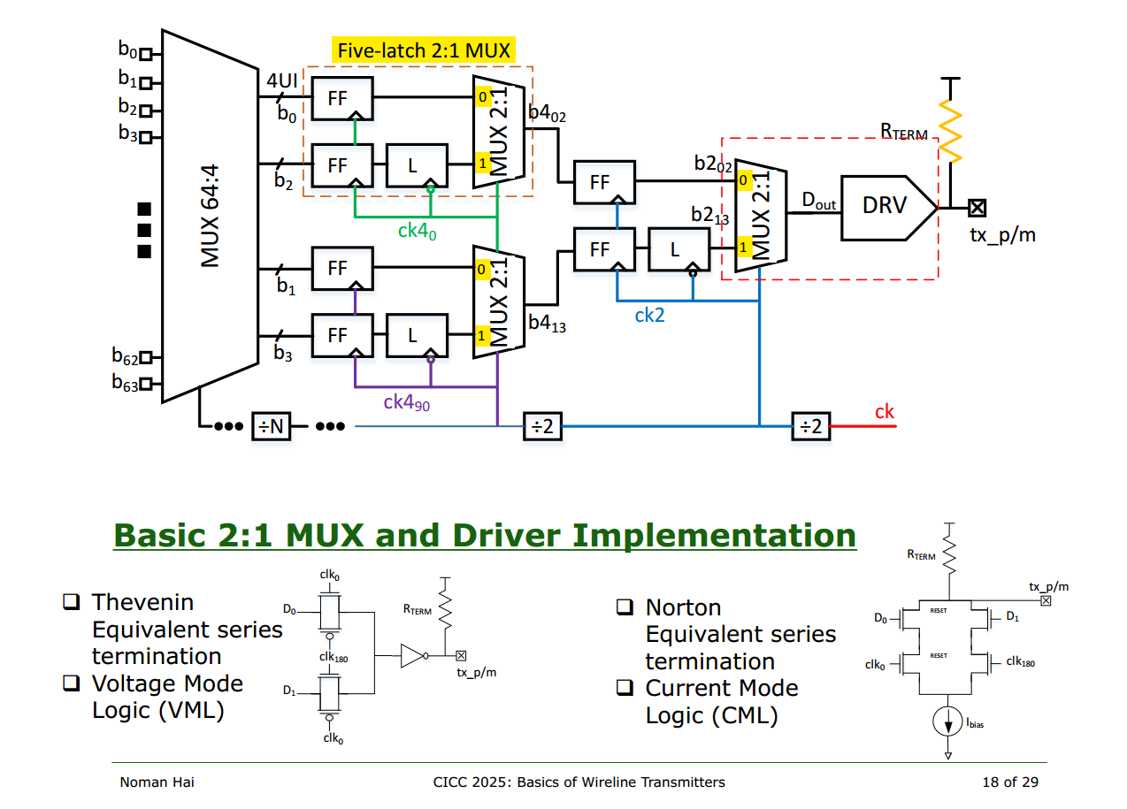
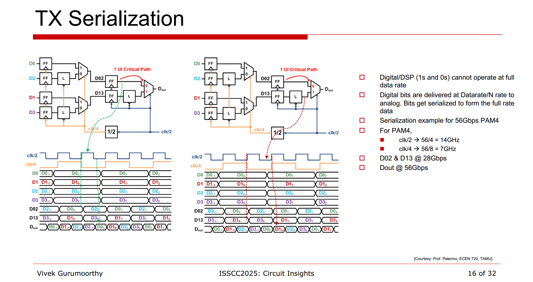

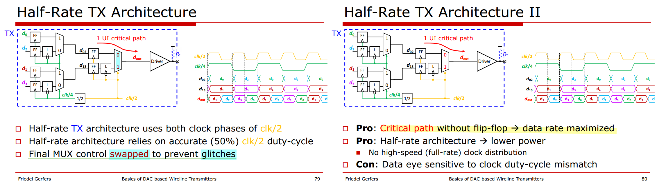
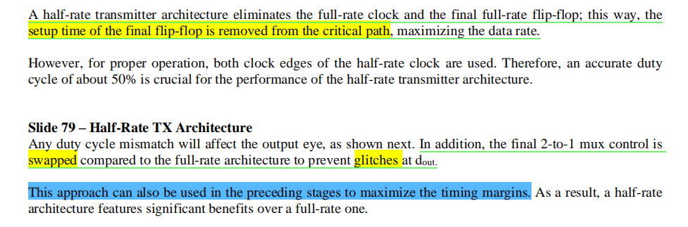

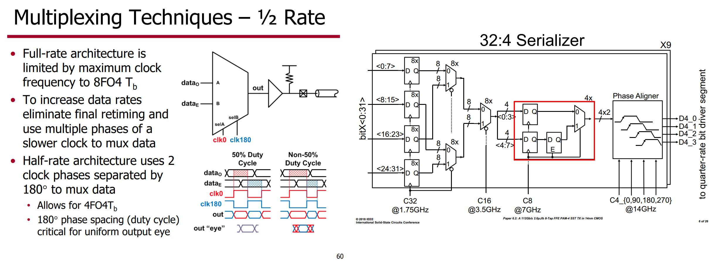
The half period that second-half selection "wastes" is deliberate slack: it lets each input settle fully before it is passed. You're trading a little latency for robustness, and designers almost always take that trade. If latency truly mattered, the better move would be to trim pipeline stages or the FIFO depth elsewhere, not to remove the settling slack from the highest-speed MUX.
Quarter-rate TX architecture
Z. Toprak-Deniz et al., "6.6 A 128Gb/s 1.3pJ/b PAM-4 Transmitter with Reconfigurable 3-Tap FFE in 14nm CMOS," 2019 IEEE International Solid-State Circuits Conference - (ISSCC), San Francisco, CA, USA, 2019, pp. 122-124 [https://sci-hub.ru/10.1109/ISSCC.2019.8662479]
—, "A 128-Gb/s 1.3-pJ/b PAM-4 Transmitter With Reconfigurable 3-Tap FFE in 14-nm CMOS," in IEEE Journal of Solid-State Circuits, vol. 55, no. 1, pp. 19-26, Jan. 2020 [https://sci-hub.ru/10.1109/JSSC.2019.2939081]
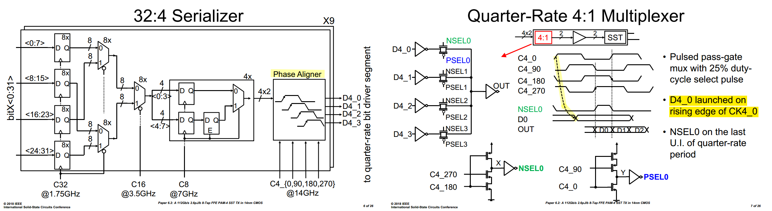
Quarter-Rate: A clocking or sampling architecture where the internal circuit clock runs at one-fourth (1/4) of the total serial data rate
Quadrature: A relationship between two signals or clocks that have a 90o phase difference (a quarter of a complete wave cycle), commonly used for I/Q modulation, directional tracking in encoders, or generating multi-phase clocks
quadrature quarter-rate (C4)
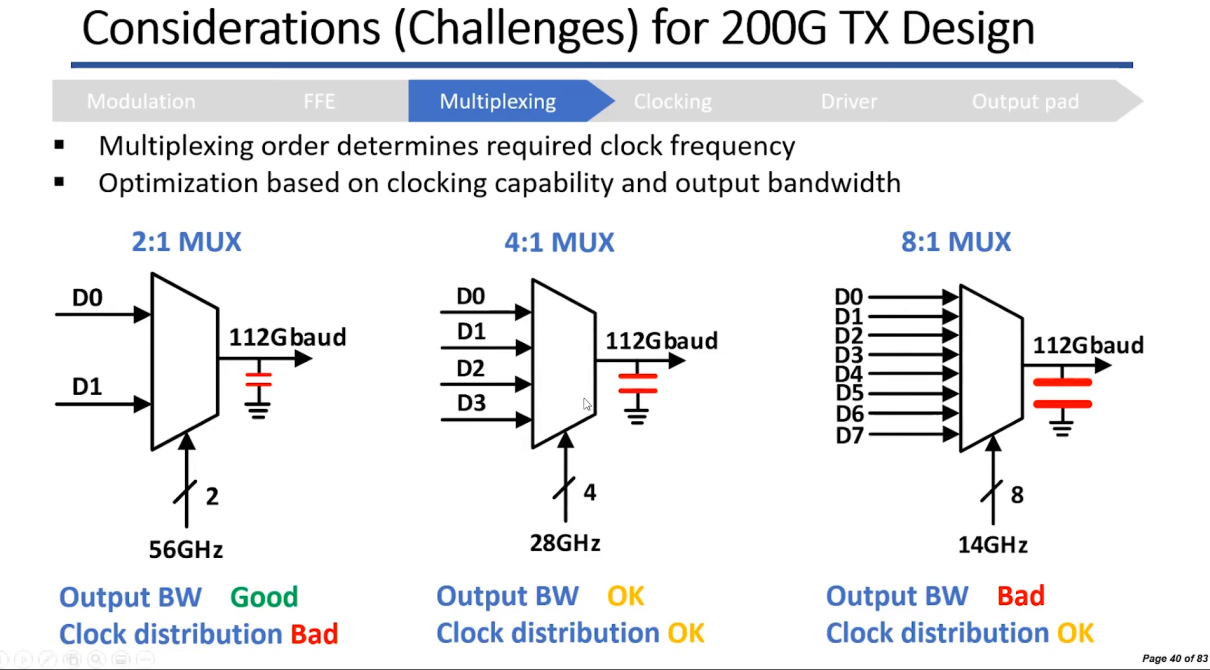
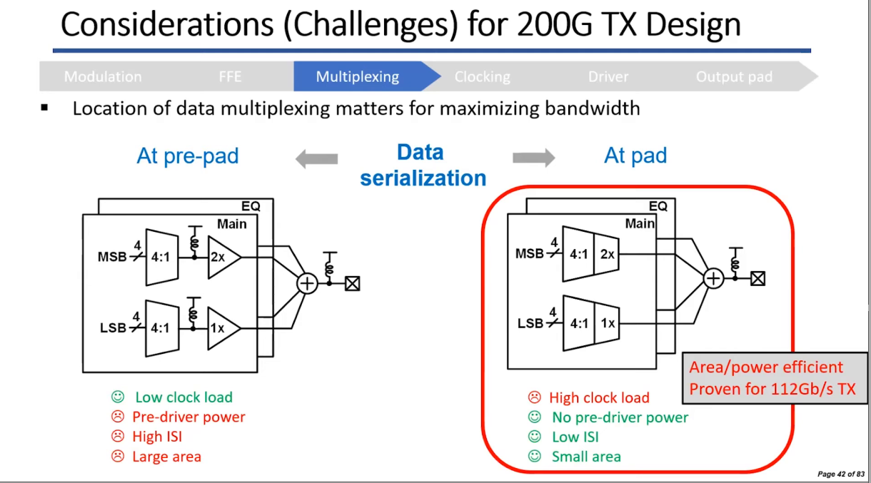
Fig. 5(c): The 2-UI pulse D1′ is carved by C4IB alone — it starts on C4IB rising and ends on C4IB falling. For the D1 → D1′ stage, the margins are 1.5 UI before and 0.5 UI after, which is asymmetric
Fig. 5(d): D1′ is the 1-UI pulse, C4IB isn't the only reference — It starts on C4IB rising, but it ends on C4Q falling, as the arrows in the figure show. The pulse generator is enabled only while C4IB and C4Q are both high
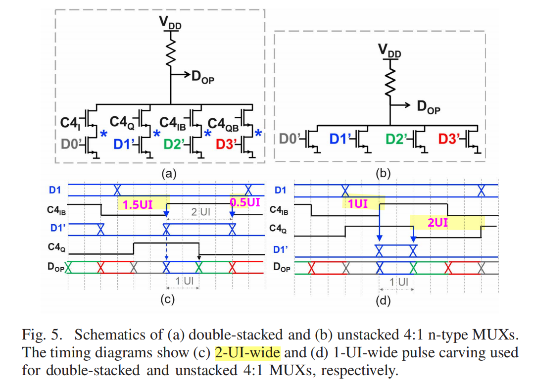
| Case | Window D1 must be stable over | Before | After |
|---|---|---|---|
| (c) D1 → D1′ | C4IB high (2 UI) | 1.5 UI | 0.5 UI |
| (c) D1 → D_OP | C4IB high and C4Q high (1 UI) | 1.5 UI | 1.5 UI |
| (d) D1 → D1′ | C4IB high and C4Q high (1 UI) | 1 UI | 2 UI |
The 0.5 UI in Fig. 5(c) is an idealized drawing, not a real delay value. In silicon, the D1 edge occurs at the launching C4 edge plus the latch clock-to-Q delay plus wiring delay. The authors drew it at 0.5 UI to show the ideal centered placement with symmetric margin
The two sub-figures place D1 differently, which shows the data-to-clock offset is set by design and illustration choices. The real requirement is only that D1 is stable, with margin, whenever its carving gate is enabled
If the natural delay lands too close to an active edge, the designer can fix it by choosing a different launching clock phase or adding delay
Synchronized divider
M. A. Kossel et al., "8.3 An 8b DAC-Based SST TX Using Metal Gate Resistors with 1.4pJ/b Efficiency at 112Gb/s PAM-4 and 8-Tap FFE in 7nm CMOS," 2021 IEEE International Solid-State Circuits Conference (ISSCC), San Francisco, CA, USA, 2021, pp. 130-132 [https://sci-hub.ru/10.1109/ISSCC42613.2021.9365784]
Michael Perrott August 12, 2008, Short Course On Phase-Locked Loops and Their Applications Day 2, PM Lecture Basic Building Blocks (Part II) High Speed Frequency Dividers, Phase Detectors, Charge Pumps, and Loop Filter Design [https://cppsim.org/PLL_Lectures/day2_pm.pdf]
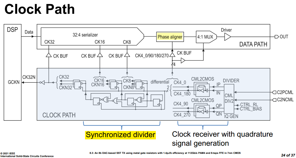
The lower speed sub-rate clocks are then obtained using a synchronous divider based on conventional master-slave flip-flops
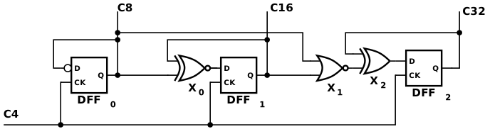

The preceding synchronous divider is equivalent to the synchronous implementation described below
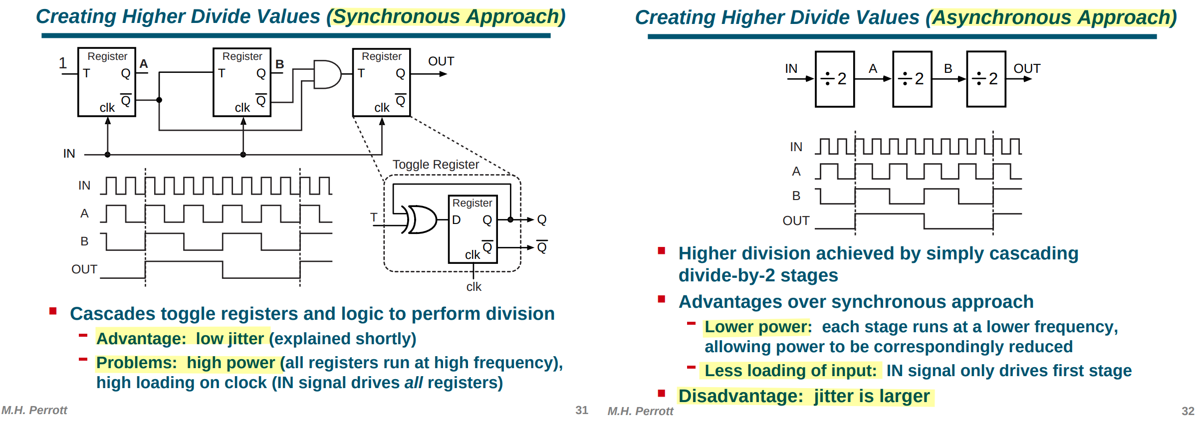
Each stage's toggle decision is computed from the states of all previous stages, but its timing comes only from the common input clock
SST Driver
sharing termination in SST transmitter

Sharing termination keep a constant current through leg, which improve TX speed in this way. On the other hand, the sharing termination facilitate drain/source sharing technique in layout.
pull-up and pull-down resistor
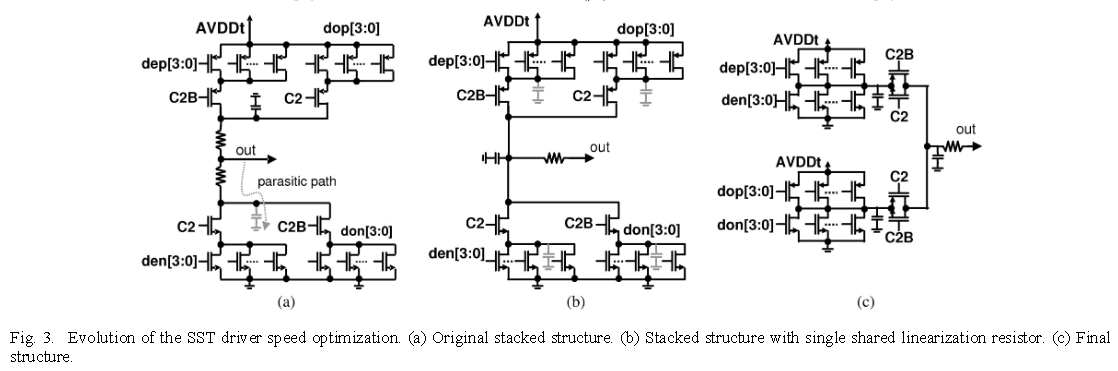
Original stacked structure
Pro's:
smaller static current when both pull up and pull down path is on
Con's:
slowly switching due to parasitic capacitance behind pull-up and pull-down resistor
with single shared linearization resistor
Pro's:
The parasitic capacitance behind the resistor still exists but is now always driven high or low actively
Con's:
more static current
VM Driver Equalization - differential ended termination
\[ V_o = D_{n+1}C_{-1}+D_nC_0+D_{n-1}C_{+1} \]
where \(D_n \in \{-1, 1\}\)
 \[
V_{\text{rx}} = V_{\text{dd}} \frac{(R_2-R_1)R_T}{R_1R_T+R_2R_T+R_1R_2}
\] With \(\color{blue}R_u=(L+M+N)R_T\)
\[
V_{\text{rx}} = V_{\text{dd}} \frac{(R_2-R_1)R_T}{R_1R_T+R_2R_T+R_1R_2}
\] With \(\color{blue}R_u=(L+M+N)R_T\)
Normalize above equation, obtain \[ V_{\text{rx,norm}} = \frac{(R_2-R_1)R_T}{R_1R_T+R_2R_T+R_1R_2} \]
| \(D_{n-1}\) | \(D_{n}\) | \(D_{n+1}\) | |
|---|---|---|---|
| \(C_{-1}\) | 1 | -1 | -1 |
| \(C_0\) | -1 | 1 | -1 |
| \(C_{+1}\) | -1 | -1 | 1 |
Where precursor \(R_L = L\times R_T\), main cursor \(R_M = M\times R_T\) and post cursor \(R_N = N\times R_T\)
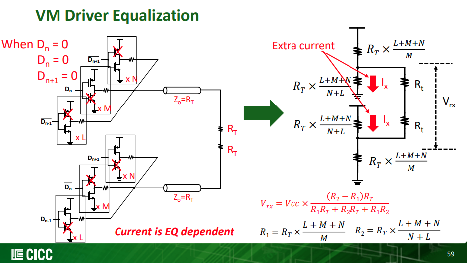
Equation-1
\(D_{n-1}D_nD_{n+1}=1,-1,-1\)

\[ R_1 = R_N = \frac{R_u}{N} \qquad\qquad R_2 = R_L\parallel R_M = \frac{R_u}{L+M} \]
We obtain \[ V_{L}= \frac{1}{2}\cdot\frac{N-(L+M)}{L+M+N} \]
Equation-2
\(D_{n-1}D_nD_{n+1}=-1,1,-1\)

with \(R_1=R_T\) and \(R_2=+\infty\), we obtain \[ V_M = \frac{1}{2} \]
Equation-3
\(D_{n-1}D_nD_{n+1}=-1,-1,1\)
\[\begin{align} R_1 &= R_L \\ &= \frac{R_u}{L} \\ R_2 &= R_N\parallel R_M \\ &= \frac{R_u}{N+M} \end{align}\]
We obtain \[ V_N = \frac{1}{2}\cdot\frac{L-(N+M)}{L+M+N} \]
Obtain FIR coefficients
We define \[\begin{align} l &= \frac{L}{L+M+N} \\ m &= \frac{M}{L+M+N} \\ n &= \frac{N}{L+M+N} \end{align}\]
where \(l+m+n=1\)
Due to Eq1 ~ Eq3 \[ \left\{ \begin{array}{cl} C_{-1}-C_0-C_1 & = \frac{1}{2}(n-l-m) \\ -C_{-1}+C_0-C_1 & = \frac{1}{2} \\ -C_{-1}-C_0+C_1 & = \frac{1}{2}(l-n-m) \end{array} \right. \] After scaling, we get \[ \left\{ \begin{array}{cl} C_{-1}-C_0-C_1 & = -l-m+n \\ -C_{-1}+C_0-C_1 & = l+m+n \\ -C_{-1}-C_0+C_1 & = l-m-n \end{array} \right. \] Then, the relationship between FIR coefficients and legs is clear, i.e. \[\begin{align} C_{-1} &= -\frac{L}{L+M+N} \\ C_{0} &= \frac{M}{L+M+N} \\ C_{1} &= -\frac{N}{L+M+N} \end{align}\]
For example, \(C_{-1}=-0.1\), \(C_0=0.7\) and \(C_1=-0.2\) \[
H(z) = -0.1+0.7z^{-1}-0.2z^{-2}
\] 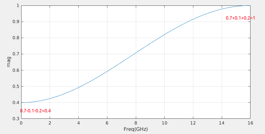
1 | w = [-0.1, 0.7, -0.2]; |
VM Driver Equalization - single ended termination
Equation-1

\[\begin{align} V_{\text{rxp}} &= \frac{1}{2} \cdot \frac{N}{L+M+N} \\ V_{\text{rxm}} &= \frac{1}{2} \cdot \frac{L+M}{L+M+N} \end{align}\] So \[ V_{L}= \frac{1}{2}\cdot\frac{N-(L+M)}{L+M+N} \] which is same with differential ended termination
Equation-2

\[\begin{align} V_{\text{rxp}} &= \frac{1}{2} \\ V_{\text{rxm}} &= 0 \end{align}\] So \[ V_{M}= \frac{1}{2} \] which is same with differential ended termination
Equation-3 \[ V_{N}= \frac{1}{2}\cdot\frac{L-(N+M)}{L+M+N} \]
Obtain FIR coefficients
Same with differential ended termination driver.
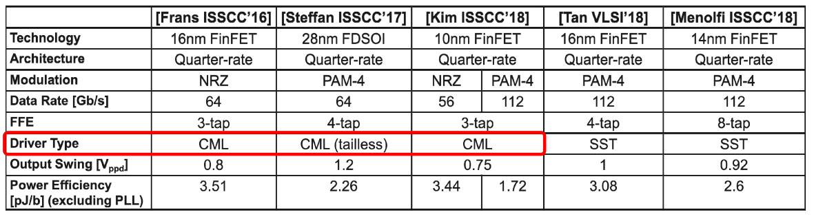
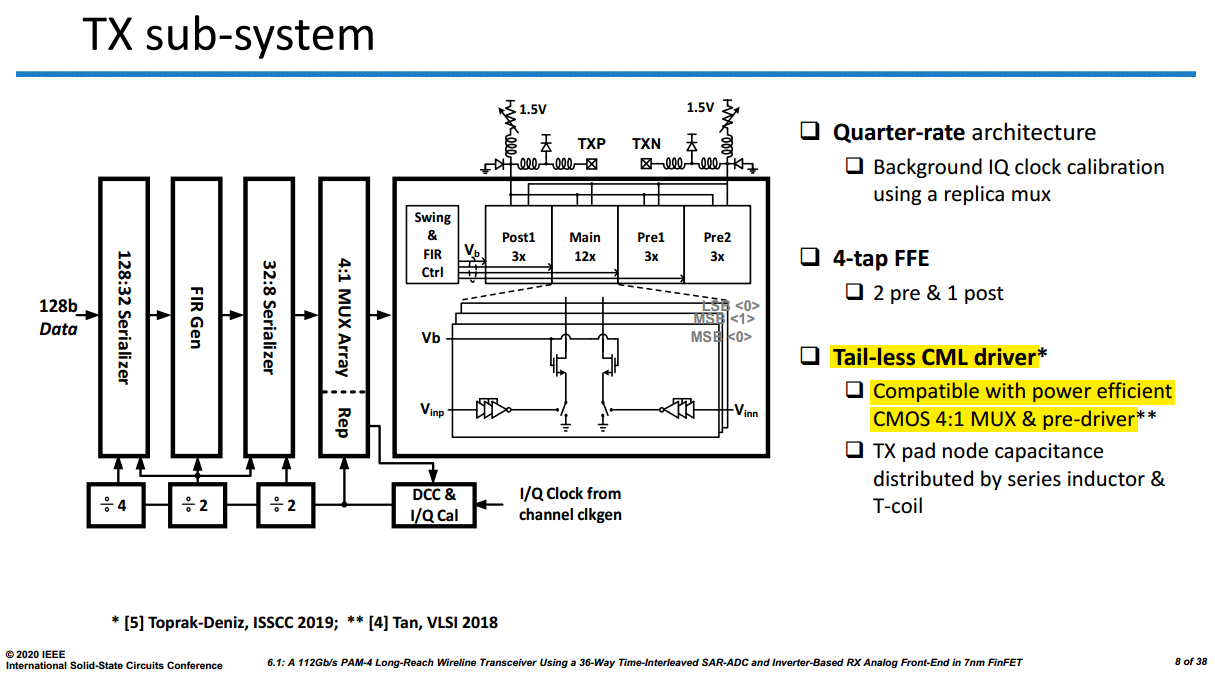
Tailless CML driver
G. Steffan et al., "6.4 A 64Gb/s PAM-4 transmitter with 4-Tap FFE and 2.26pJ/b energy efficiency in 28nm CMOS FDSOI," 2017 IEEE International Solid-State Circuits Conference (ISSCC), San Francisco, CA, USA, 2017, pp. 116-117 [https://sci-hub.ru/10.1109/ISSCC.2017.7870288]
Z. Toprak-Deniz et al., "A 128-Gb/s 1.3-pJ/b PAM-4 Transmitter With Reconfigurable 3-Tap FFE in 14-nm CMOS," in IEEE Journal of Solid-State Circuits, vol. 55, no. 1, pp. 19-26, Jan. 2020 [https://sci-hub.ru/10.1109/JSSC.2019.2939081]
J. Im et al., "6.1 A 112Gb/s PAM-4 Long-Reach Wireline Transceiver Using a 36-Way Time-Interleaved SAR-ADC and Inverter-Based RX Analog Front-End in 7nm FinFET," 2020 IEEE International Solid-State Circuits Conference - (ISSCC), San Francisco, CA, USA, 2020, pp. 116-118 [https://sci-hub.ru/10.1109/ISSCC19947.2020.9063081
a.k.a. Pseudo - CML
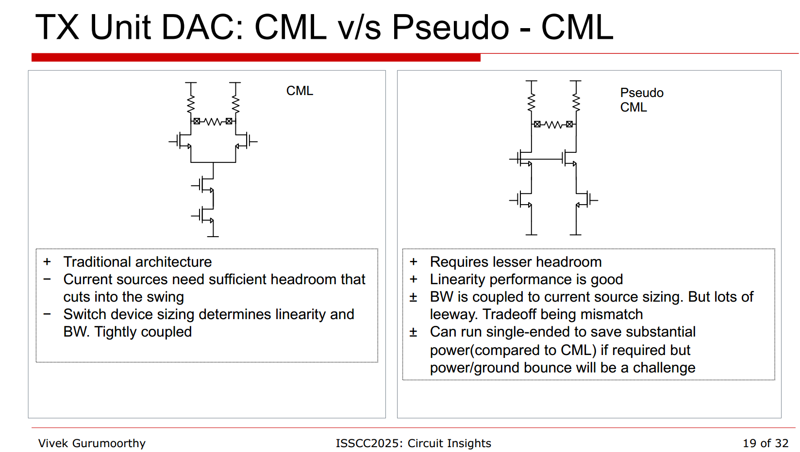
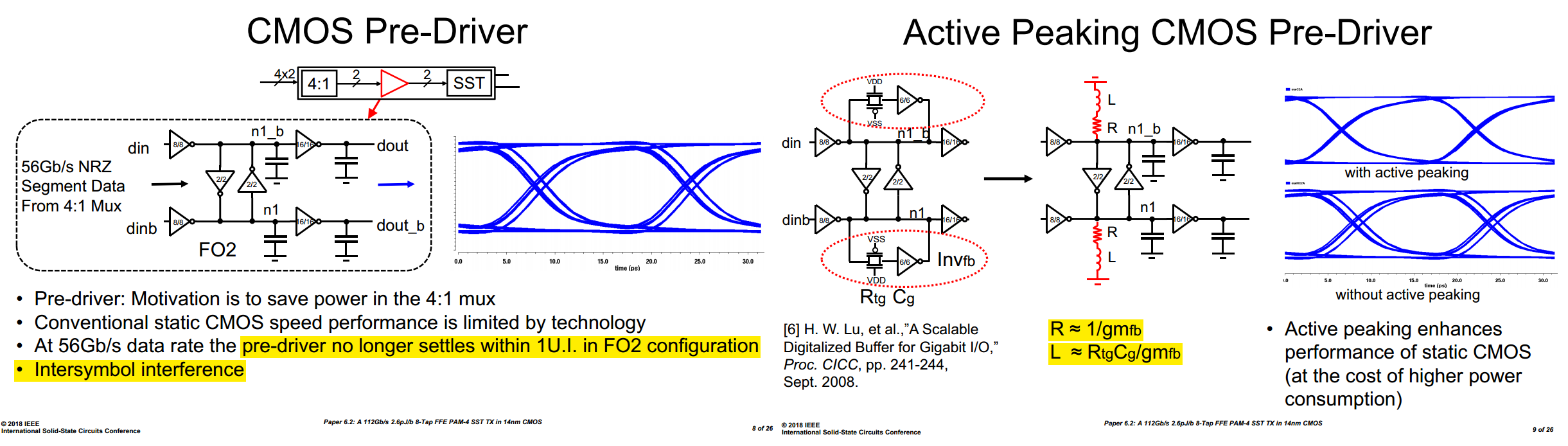
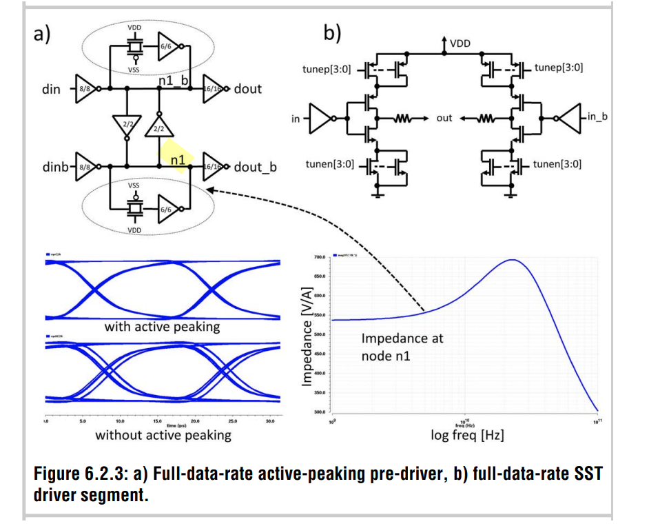
Active Peaking CMOS Pre-Driver
C. Menolfi et al., "A 112Gb/S 2.6pJ/b 8-Tap FFE PAM-4 SST TX in 14nm CMOS," 2018 IEEE International Solid-State Circuits Conference - (ISSCC), San Francisco, CA, USA, 2018, pp. 104-106 [https://sci-hub.ru/10.1109/ISSCC.2018.8310205]
HungWen Lu, ChauChin Su and Chien-Nan Liu, "A scalable digitalized buffer for gigabit I/O," 2008 IEEE Custom Integrated Circuits Conference, San Jose, CA, USA, 2008, pp. 241-244 [https://sci-hub.ru/10.1109/CICC.2008.4672068]
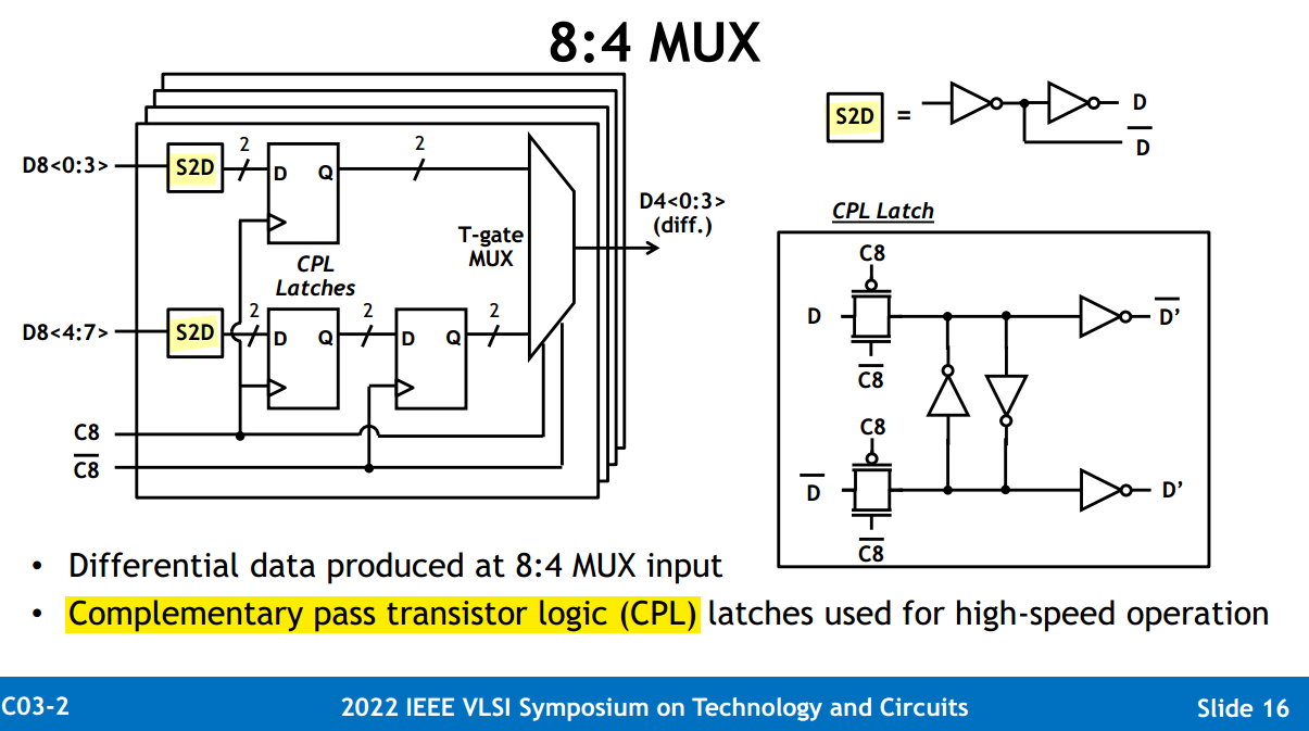
Single-Ended-to-Differential (S2D)
T. Dickson et al., "C3.2 A 72GS/s, 8-bit DAC-based Wireline Transmitter in 4nm FinFET CMOS for 200+Gb/s Serial Links," 2022 IEEE Symposium on VLSI Technology and Circuits (VLSI Technology and Circuits), Honolulu, HI, USA, 2022, pp. 28-29 [https://sci-hub.ru/10.1109/VLSITechnologyandCir46769.2022.9830421]
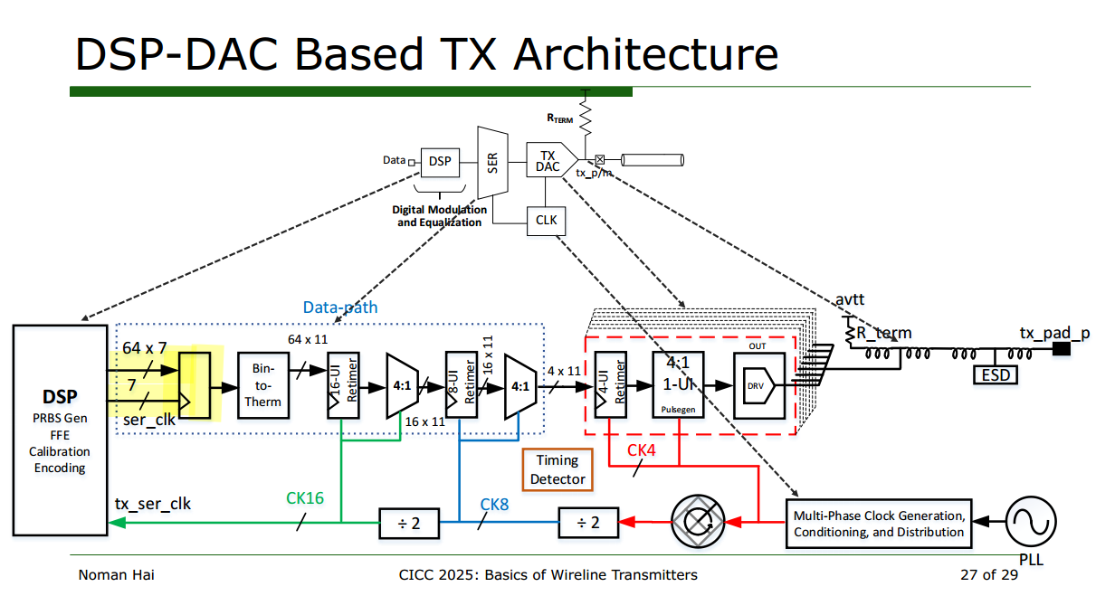
CDC between DSP and Seralizer
Peak power constraint of TX FIR
Kevin Zheng , Circuit Insights @ ISSCC2025: Circuits for Wireline Communications [https://youtu.be/8NZl81Dj45M&t=829]
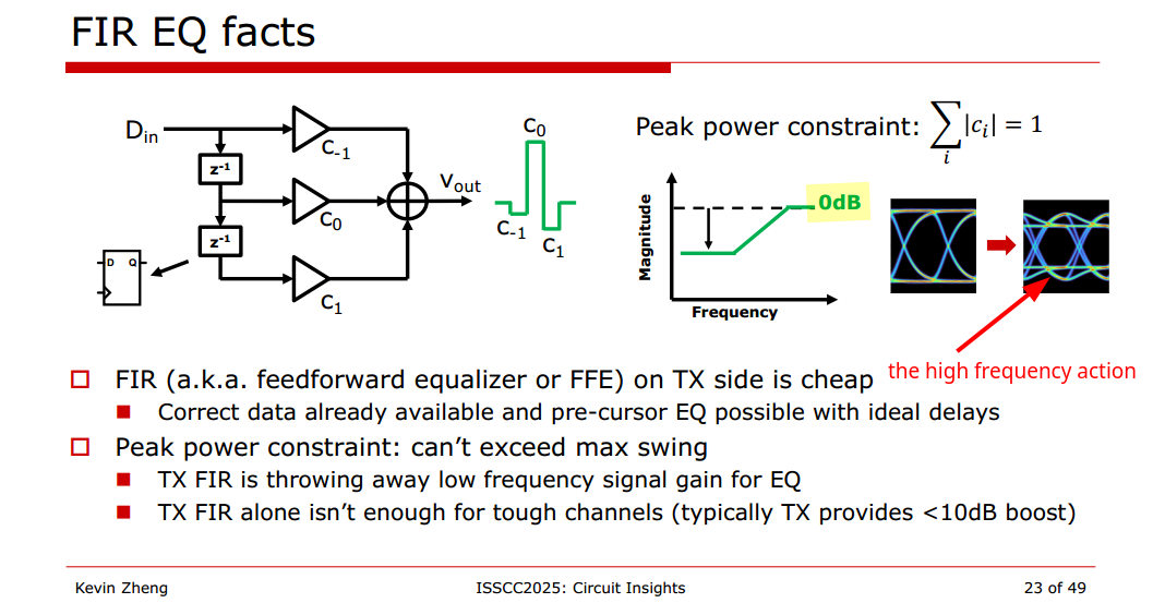
Due to circuit limitation, circuit cannot have arbitrarily large voltage on the output, i.e. a limited maximum swing. In order to create the high frequency shape, the best we can do is lower DC gain (low frequency gain < 1)
- FIR is not increasing the amplitude on the edges
- FIR is reducing the inner eye diagram
The maximum swing stays the same, \(\sum_i |c_i|=1\)
0.5b in segmented DAC
Z. Guo et al., "6.2 A 112.5Gb/s ADC-DSP-Based PAM-4 Long-Reach Transceiver with >50dB Channel Loss in 5nm FinFET," 2022 IEEE International Solid-State Circuits Conference (ISSCC), San Francisco, CA, USA, 2022, pp. 116-118 [https://sci-net.xyz/10.1109/ISSCC42614.2022.9731650]
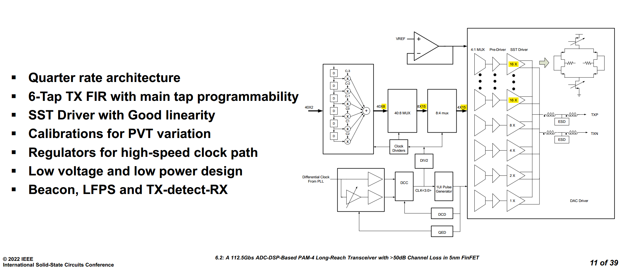
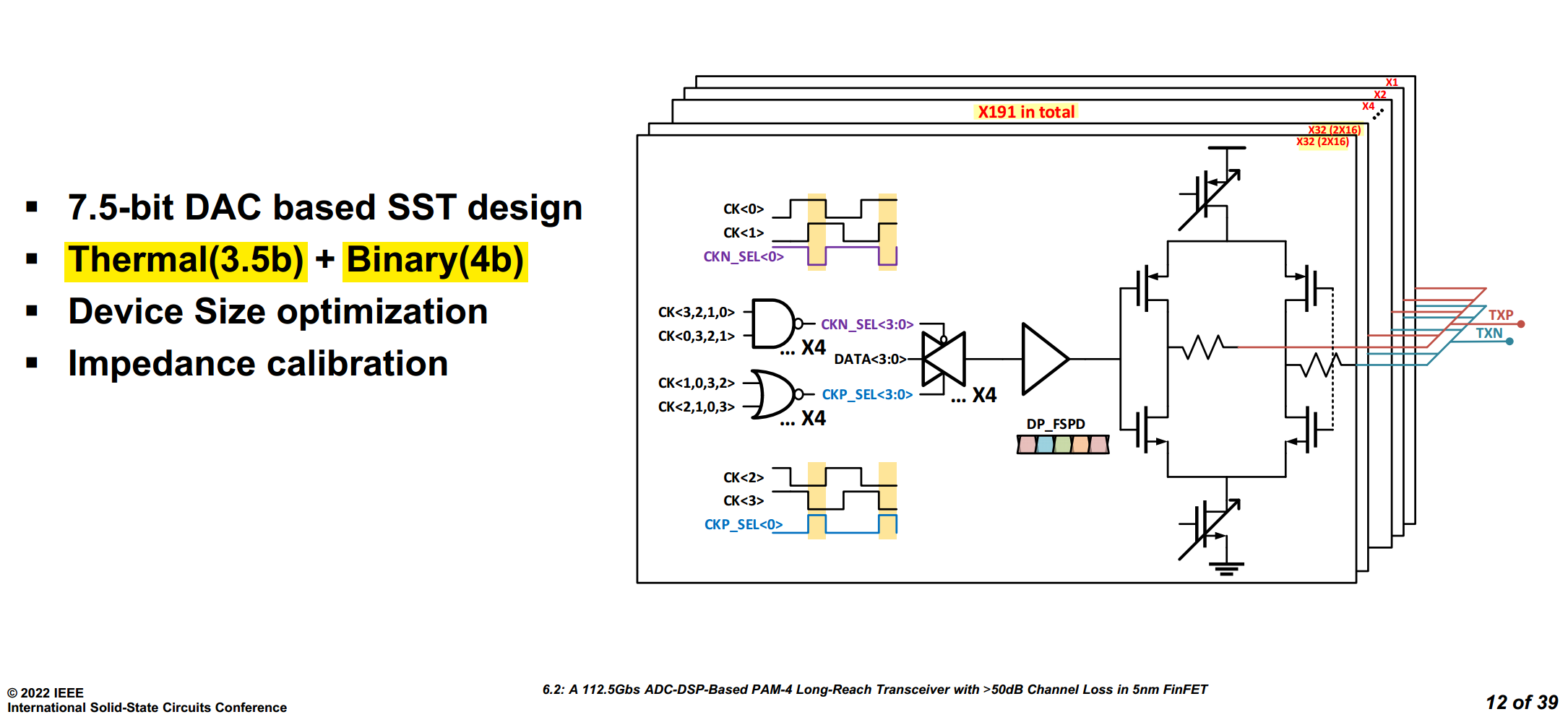
totalX = 1 +2 + 4 + 8 + (1 + 2 + 4)*16 + 4*16 = 1 +2 + 4 + 8 + 16*11 = 191
Therefore, the valid input range range is 0 ~ 191, even though the input bit number is 8 (range 0~255)
If we apply \(\log_2\) to \(\boxed{N+0.5}\) bit DAC \[ \log_2 (2^N + 2^{N-1}) = N - 1 + 3\log_2(3) = N + 0.585 \]
Basic FeedForward Equalization Theory
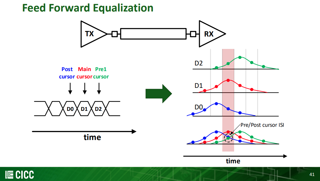
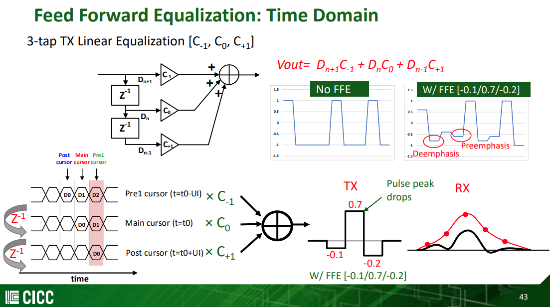
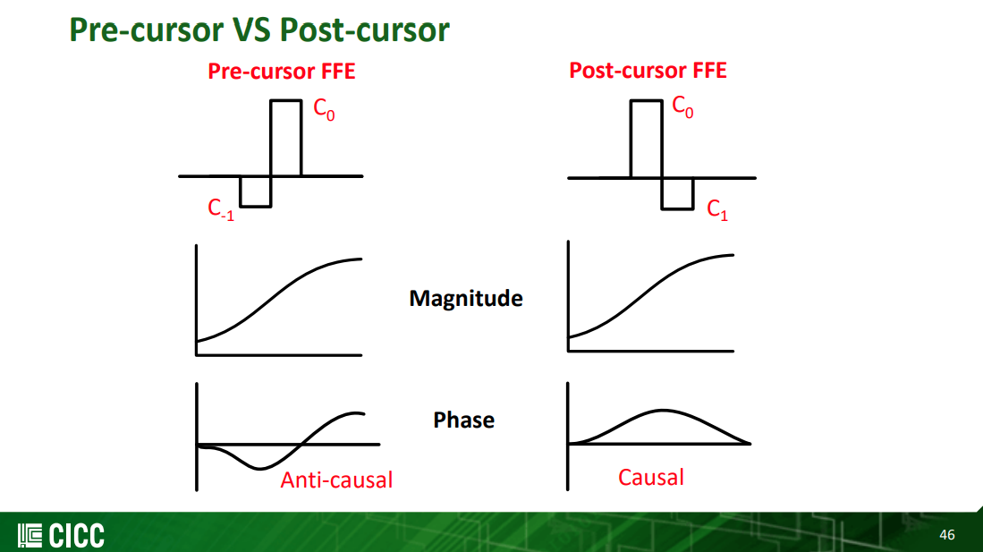
Pre-cursor FFE can compensate phase distortion through the channel
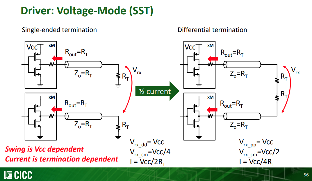
Single-ended termination
Differential termination
PAM4 TX
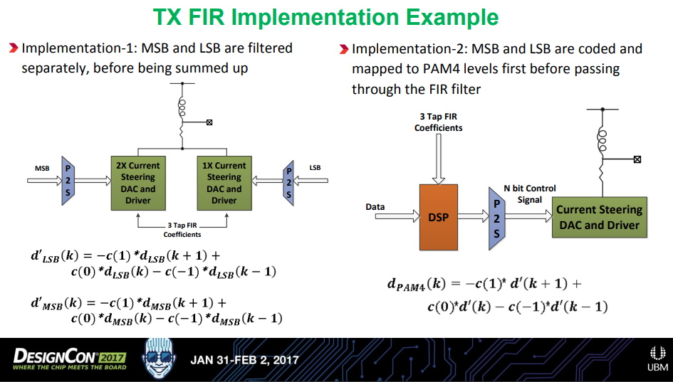
Here, \(d_{\text{LSB}} \in \{-1, 1\}\), \(d_{\text{MSB}} \in \{-2, 2\}\) and \(d' \in \{ -3, -1, 1, 3 \}\)
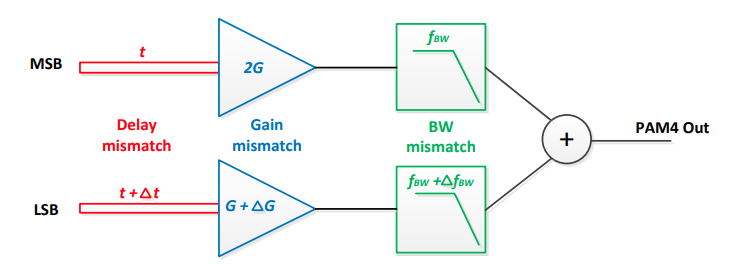
Implementation-1 could potentially experience performance degradation due to
- Clock skew, \(\Delta t\), could make the eye misaligned horizontally
- Gain mismatch, \(\Delta G\), could cause eye nonlinearity
- Bandwidth mismatch, \(\Delta f_{\text{BW}}\), could make the eye misaligned vertically
Typically, a 3-tap FIR (pre + main + post) TX de-emphasis is used
3-tap FIR results in \(4^3 = 64\) possible distinct signal levels

\[\begin{align} R_U^M \parallel R_D^M &= \frac{3R_T}{2}\\ R_U^L \parallel R_D^L &= 3R_T \end{align}\]
Thevenin Equivalent Circuit is 
Which can be simpified as  \[\begin{align}
V_{\text{rx}} &= \frac{1}{2}(V_p - V_m) \\
&= \frac{1}{2}(\frac{2}{3}(2V_{\text{MSB}}+V_{\text{LSB}})-1) \\
&=\frac{1}{3}(2V_{\text{MSB}}+V_{\text{LSB}})-\frac{1}{2}
\end{align}\]
\[\begin{align}
V_{\text{rx}} &= \frac{1}{2}(V_p - V_m) \\
&= \frac{1}{2}(\frac{2}{3}(2V_{\text{MSB}}+V_{\text{LSB}})-1) \\
&=\frac{1}{3}(2V_{\text{MSB}}+V_{\text{LSB}})-\frac{1}{2}
\end{align}\]
The above eqations demonstrate that the output \(V_{\text{rx}}\) is the linear sum of MSB and LSB; LSB and MSB have relative weight, i.e. 1 for LSB and 2 for MSB.
Assume pre cusor has \(L\) legs, main cursor \(M\) legs and post cursor \(N\) legs, which is same with the convention in "Voltage-Mode Driver Equalization"
The number of legs connected with supply can expressed as \[ n_{up} = (1-d_{n+1})L + d_{n}M + (1-d_{n-1})N \] Where \(d_n \in \{0, 1\}\), or \[ n_{up} = \frac{1}{2}(-D_{n+1}+1)L + \frac{1}{2}(D_{n}+1)M + \frac{1}{2}(-D_{n-1}+1)N \] Where \(D_n \in \{-1, +1\}\)
Then the number of legs connected with ground is \[ n_{dn}=L+M+N-n_{up} \] where \(n_{up}+n_{dn}=L+M+N\)
Voltage resistor divider \[\begin{align} V_o &= \frac{\frac{R_{U}}{n_{dn}}}{\frac{R_U}{n_{dn}}+\frac{R_U}{n_{up}}} \\ &= \frac{1}{2}- \frac{1}{2}D_{n+1}\frac{L}{L+M+N}+ \frac{1}{2}D_{n}\frac{M}{L+M+N}-\frac{1}{2}D_{n-1}\frac{N}{L+M+N} \\ &= \frac{1}{2}-\frac{1}{2}D_{n+1}\cdot l+ \frac{1}{2}D_{n}\cdot m-\frac{1}{2}D_{n-1}\cdot n \end{align}\]
where \(l+m+n=1\)
\(V_{\text{MSB}}\) and \(V_{\text{LSB}}\) can be obtained
\[\begin{align} V_{\text{MSB}} &= \frac{1}{2}-\frac{1}{2}D^{\text{MSB}}_{n+1}\cdot l+ \frac{1}{2}D^{\text{MSB}}_{n}\cdot m-\frac{1}{2}D^{\text{MSB}}_{n-1}\cdot n \\ V_{\text{LSB}} &= \frac{1}{2}-\frac{1}{2}D^{\text{LSB}}_{n+1}\cdot l+ \frac{1}{2}D^{\text{LSB}}_{n}\cdot m-\frac{1}{2}D^{\text{LSB}}_{n-1}\cdot n \end{align}\]
Substitute the above equation into \(V_{\text{rx}}\), we obtain the relationship between driver legs and FFE coefficients
\[\begin{align} V_{\text{rx}} &=\frac{1}{3}(2V_{\text{MSB}}+V_{\text{LSB}})-\frac{1}{2} \\ &= \frac{1}{3} \left\{ 2\left( \frac{1}{2}-\frac{1}{2}D^{\text{MSB}}_{n+1}\cdot l+ \frac{1}{2}D^{\text{MSB}}_{n}\cdot m- \frac{1}{2}D^{\text{MSB}}_{n-1}\cdot n \right) + \left( \frac{1}{2}-\frac{1}{2}D^{\text{LSB}}_{n+1}\cdot l+ \frac{1}{2}D^{\text{LSB}}_{n}\cdot m- \frac{1}{2}D^{\text{LSB}}_{n-1}\cdot n \right) \right\}-\frac{1}{2} \\ &= \left(-\frac{l}{6} \cdot 2 \cdot D^{\text{MSB}}_{n+1}+ \frac{m}{6} \cdot 2 \cdot D^{\text{MSB}}_{n}- \frac{n}{6} \cdot 2 \cdot D^{\text{MSB}}_{n-1}\right) + \left(-\frac{l}{6} \cdot D^{\text{LSB}}_{n+1}+ \frac{m}{6} \cdot D^{\text{LSB}}_{n}- \frac{n}{6} \cdot D^{\text{LSB}}_{n-1}\right) \\ &= -\frac{l}{6}(2 \cdot D^{\text{MSB}}_{n+1}+D^{\text{LSB}}_{n+1})+ \frac{m}{6}(2\cdot D^{\text{MSB}}_{n}+D^{\text{LSB}}_{n}) -\frac{n}{6}(2\cdot D^{\text{MSB}}_{n-1}+D^{\text{LSB}}_{n-1}) \end{align}\]
After scaling, we obtain \[ V_{\text{rx}} = -l\cdot(2 \cdot D^{\text{MSB}}_{n+1}+D^{\text{LSB}}_{n+1})+ m\cdot(2\cdot D^{\text{MSB}}_{n}+D^{\text{LSB}}_{n}) - n \cdot(2\cdot D^{\text{MSB}}_{n-1}+D^{\text{LSB}}_{n-1}) \] Where \(C_{-1} = l\), \(C_0 = m\) and \(C_{1}=n\), which is same with that of NRZ
Eye Linearity vs. RLM (Relative Level Mismatch)
Chaowaroj (Max) Wanotayaroj. Introduction to PAM4 [https://indico.cern.ch/event/979659/contributions/4127016/attachments/2159338/3642883/PAM4Eval%20-%20Dec2020%20Seminar.pdf]
TODO 📅
Tx Measurements
PAM4 Transmitter Test Challenges [https://harrisburg.psu.edu/files/pdf/16861/2019/05/06/tektronix_penn_state_si_april_12_2019.pdf]
PAM4 Signaling in High Speed Serial Technology: Test, Analysis, and Debug [https://download.tek.com/document/55W_60273_1_HR_Letter.pdf]
PCIe 7.0 Introduction PCIe 6.0 Anritsu/Tektronix Solution [https://map-assets.tek.com/map-assets/emea/pdf-files/PCIe7_0_Intro_PCIe_6_0_Solution.pdf]
Mike Hertz, Teledyne LeCroy: WEBINAR PAM4 Analysis and Measurement Considerations
Brandon Gore, Samtec, DesignCon 2025, Transmitter Power Spectral Density Noise Impact for 200 Gb/s PAM 4 per lane [pdf] [slides]
TODO 📅
TX Jitter Measurement
PCI-SIG, Update-on-PCIe8p0-Scope-bandwidth-study-and-jitter-measurement-Intel-2025-12-18_v3
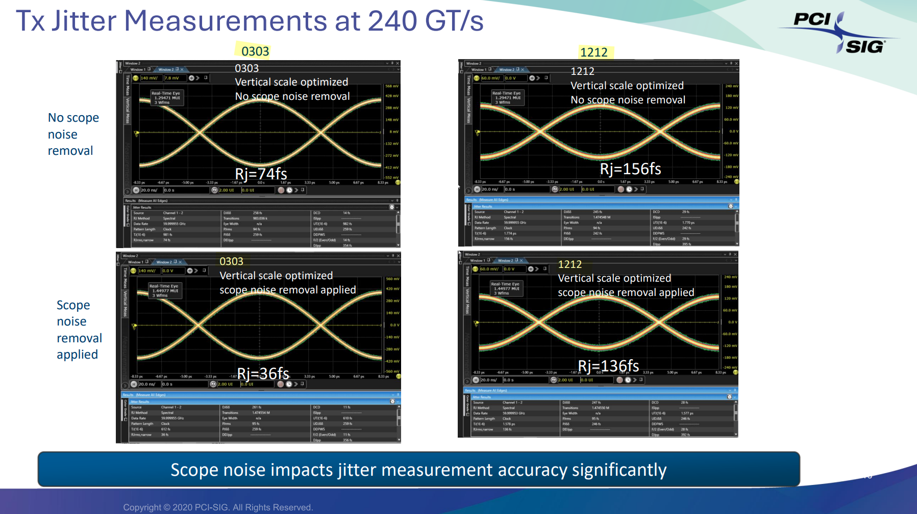
Linear Fit Pulse Response (LFPR)
Hsinho Wu, Intel. DesignCon 2021: SNDR Analysis & Its Impacts on Link Performance
Christiaan Bil (Intel), DesignCon 2026. An Experimental Study of PCIe Transmitter Equalization Preset Measurement Methods for 64 and 128 GT/s PAM4 Signaling
Dhruv Gupta, DesignCon 2026. PAM4 measurements through lossy channels – why oscilloscope CDR emulation matters
TODO 📅
SNDR
Marianne Nourzad, July 2nd, 2020 PCI-SIG ® EWG Meeting, PCIE Gen6 TX SNDR Methodology Discussion
Pegah Alavi (Keysight Technologies) DesignCon 2025: PCI Express & PAM4: Balancing Silicon and interconnect interdependencies for 128 GT/s
Rick Eads, Pegah Alavi, Randy Garrett, Keysight Technologies) DesignCon 2025, The Road to PCIe 7.0: Advanced Testing Challenges at 64 GBaud PAM4 [https://www.keysight.com/us/en/assets/9925-01141/seminar-materials/KEF-DesignCon-2025-PCIe-Eads-Presentation.pdf]
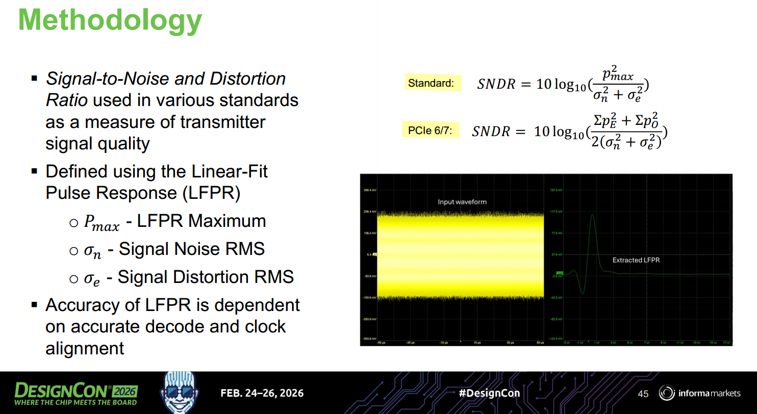
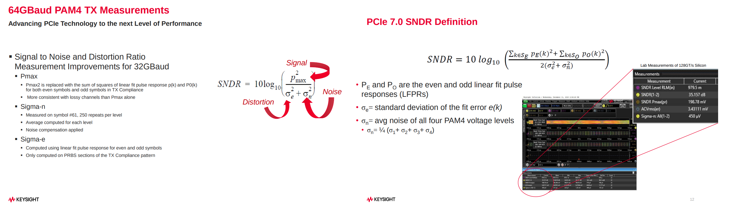
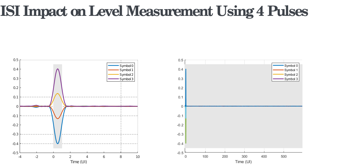
RLM Measurement Based on Multi-pulse Extraction
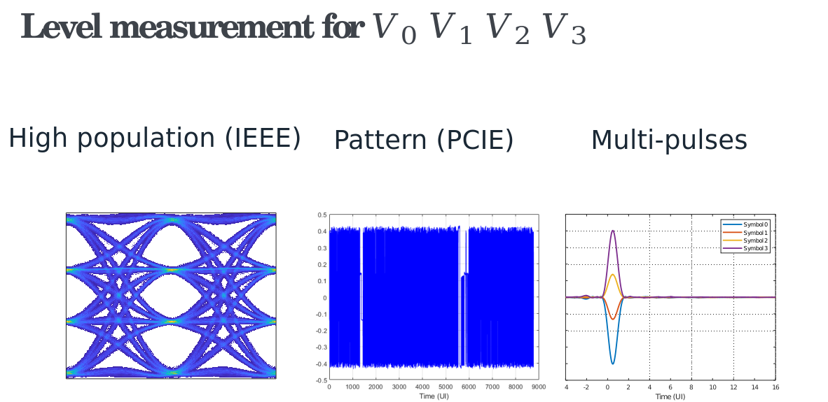
reference
Jan Mulder, ISSCC2015 T5: High-Speed Current-Steering DACs
Jihwan Kim, ISSCC2019 F5: Design Techniques for a 112Gbs PAM-4 Transmitter
—, Intel, SNU Summer 2021 [Topic] "A 200Gb/s CMOS Transmitter: Challenges and Overcoming Design Techniques" [https://youtu.be/w3lb_1TwdeE]
—, CICC 2022, ES4-4: Transmitter Design for High-speed Serial Data Communications
Friedel Gerfers, ISSCC2021 T6: Basics of DAC-based Wireline Transmitters
Noman Hai, Synopsys. CICC 2025 Circuit Insights: Basics of Wireline Transmitter Circuits [https://youtu.be/oofViBGlrjM]
—, Synopsys. Design Challenges Of High-Speed Wireline Transmitters [https://semiengineering.com/design-challenges-of-high-speed-wireline-transmitters/]
—, Synopsys. CMOS Circuit Techniques for Wireline Transmitters [https://www.synopsys.com/webinars/wireline-transmitters-part-1.html]
Vivek Gurumoorthy, Marvell, ISSCC 2025 Circuit Insights: Circuits for Optical Communication
Tod Dickson, IBM IEEE San Diego 2020. High-Speed CMOS Serial Transmitters for 56-112Gb/s Electrical Interconnects [https://www.youtube.com/watch?v=g1pcZabsRNc]
B. Razavi, "Design Techniques for High-Speed Wireline Transmitters," in IEEE Open Journal of the Solid-State Circuits Society, vol. 1, pp. 53-66, 2021 [https://www.seas.ucla.edu/brweb/papers/Journals/BROJSSCSep21.pdf]
T. Chan Carusone, T. O. Dickson, S. Palermo, S. Shekhar and M. Mansuri, "Modern Wireline Transceivers," in IEEE Journal of Solid-State Circuits, vol. 61, no. 2, pp. 395-422, Feb. 2026 [https://ieeexplore.ieee.org/stamp/stamp.jsp?arnumber=11311714]
Yvain Thonnart, CEA-LIST. ISSCC2021 T8: On-Chip Interconnects: Basic Concepts, Designs and Future Opportunities
Mozhgan Mansuri. ISSCC2021 SC3: Clocking, Clock Distribution, and Clock Management in Wireline/Wireless Subsystems
Sam Palermo. High-Performance SERDES Design" Online Course (2025): Current-Mode DAC TX [https://youtu.be/A2VsvCPDWxk]
PCIe® 6.0 Specification: The Interconnect for I/O Needs of the Future PCI-SIG® Educational Webinar Series, [https://pcisig.com/sites/default/files/files/PCIe%206.0%20Webinar_Final_.pdf]