DSP to ASIC
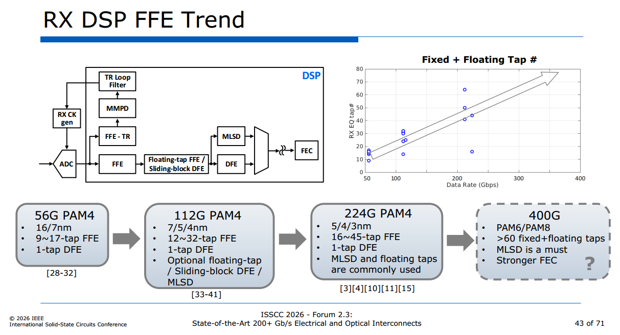
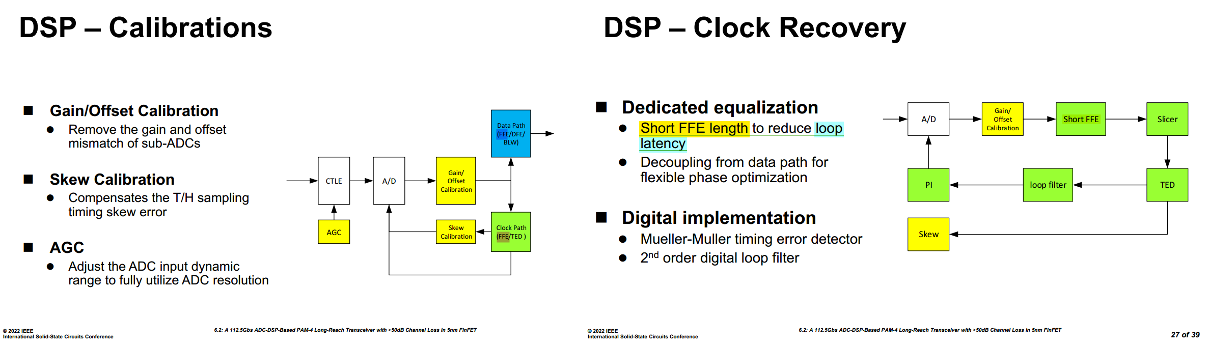
FFE in DSP
M. A. Kossel et al., "8.3 An 8b DAC-Based SST TX Using Metal Gate Resistors with 1.4pJ/b Efficiency at 112Gb/s PAM-4 and 8-Tap FFE in 7nm CMOS," 2021 IEEE International Solid-State Circuits Conference (ISSCC), San Francisco, CA, USA, 2021, pp. 130-132 [https://sci-hub.ru/10.1109/ISSCC42613.2021.9365784]
Z. Guo et al., "6.2 A 112.5Gb/s ADC-DSP-Based PAM-4 Long-Reach Transceiver with >50dB Channel Loss in 5nm FinFET," 2022 IEEE International Solid-State Circuits Conference (ISSCC), San Francisco, CA, USA, 2022, pp. 116-118 [https://sci-net.xyz/10.1109/ISSCC42614.2022.9731650]
TODO 📅
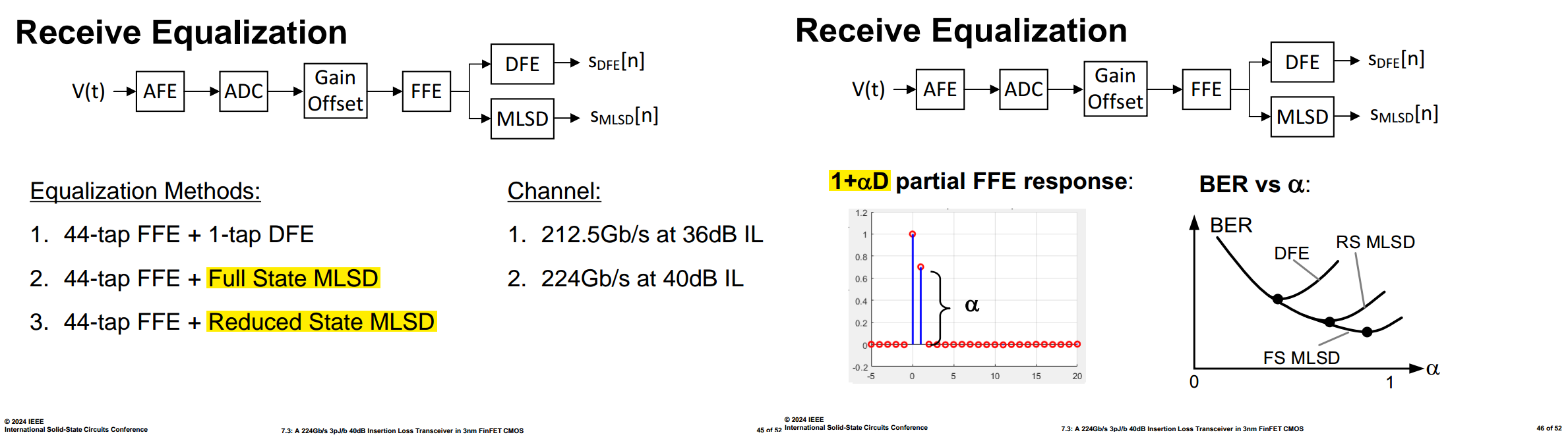
1+αD partial FFE response
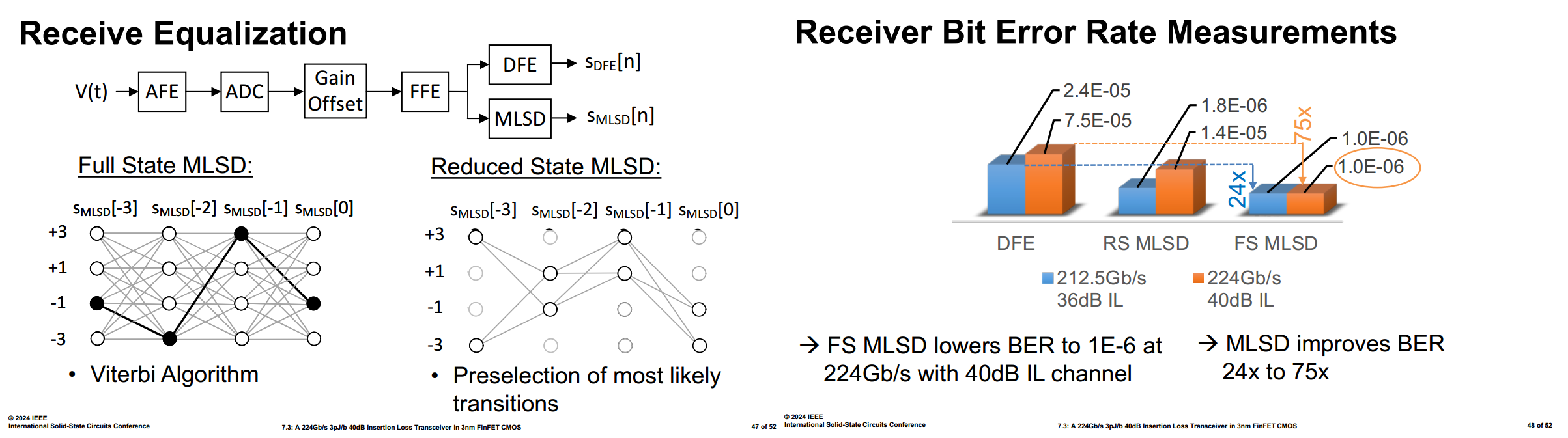
D. Pfaff et al., "7.3 A 224Gb/s 3pJ/b 40dB Insertion Loss Transceiver in 3nm FinFET CMOS," 2024 IEEE International Solid-State Circuits Conference (ISSCC), San Francisco, CA, USA, 2024, pp. 128-130 [https://sci-net.xyz/10.1109/ISSCC49657.2024.10454537]
Full State MLSD, Reduced State MLSD
DFE in DSP
Synopsys Italia, Tech Talk: Introduction to DSP-based SerDes [https://youtu.be/puEP0DlVZGI]
Chen, Kuan-Chang (2022) Energy-Efficient Receiver Design for High-Speed Interconnects. Dissertation (Ph.D.), California Institute of Technology. [https://thesis.caltech.edu/14318/09/chen_kuan-chang_2022_thesis_final.pdf]
Loop-Unrolling DFE
Y. Lu and E. Alon, "Design Techniques for a 66 Gb/s 46 mW 3-Tap Decision Feedback Equalizer in 65 nm CMOS," in IEEE Journal of Solid-State Circuits, vol. 48, no. 12, pp. 3243-3257, Dec. 2013 [https://sci-hub.ru/10.1109/JSSC.2013.2278804]
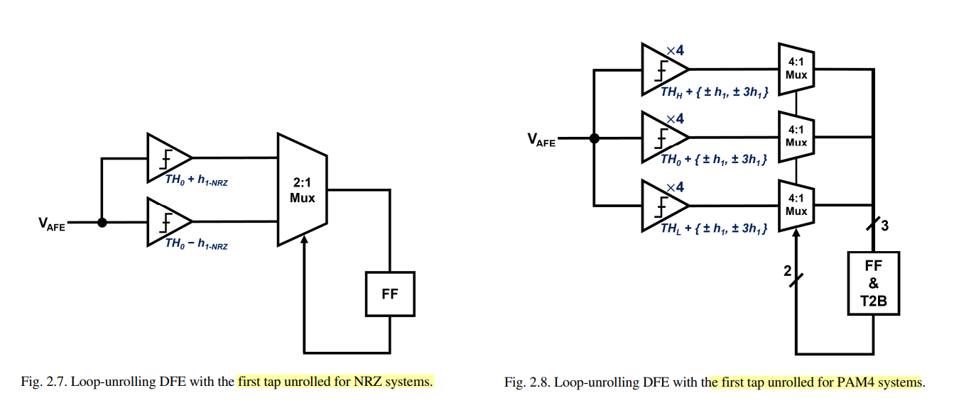
Corresponding to the three distinct voltage thresholds in the PAM4 systems, it would need 12 slicers, 3 multiplexers, and one thermometer-to-binary decoder in each deserialized data path, even if only one tap of the DFE is unrolled
Look-Ahead DFE
K. K. Parhi, "Pipelining of parallel multiplexer loops and decision feedback equalizers," 2004 IEEE International Conference on Acoustics, Speech, and Signal Processing, Montreal, QC, Canada, 2004, pp. V-21 [https://sci-hub.ru/10.1109/ICASSP.2004.1327037]
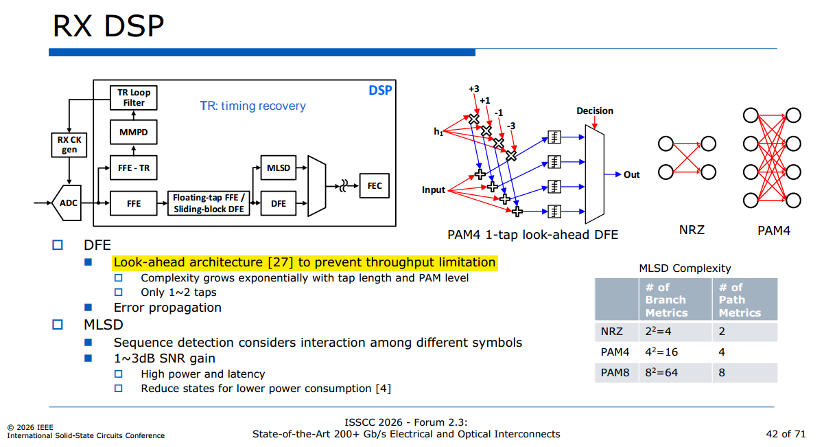
The look-ahead multiplexing technique brings the key benefit that the timing constraint can be significantly relaxed, as the iteration bound is doubled at the expense of extra hardware
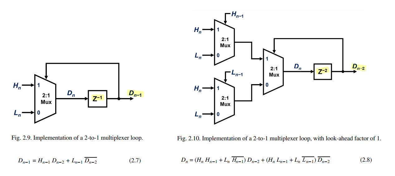
Sliding-Block DFE
J. Bailey et al., "8.8 A 112Gb/s PAM-4 Low-Power 9-Tap Sliding-Block DFE in a 7nm FinFET Wireline Receiver," 2021 IEEE International Solid-State Circuits Conference (ISSCC), San Francisco, CA, USA, 2021, pp. 140-142 [https://sci-hub.ru/10.1109/ISSCC42613.2021.9365853]
J. Bailey et al., "A 112-Gb/s PAM-4 Low-Power Nine-Tap Sliding-Block DFE in a 7-nm FinFET Wireline Receiver," in IEEE Journal of Solid-State Circuits, vol. 57, no. 1, pp. 32-43, Jan. 2022 [https://sci-hub.jp/10.1109/JSSC.2021.3109167]
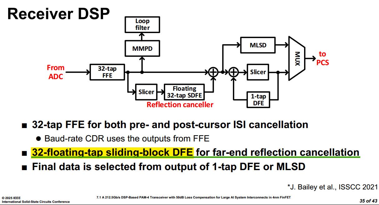
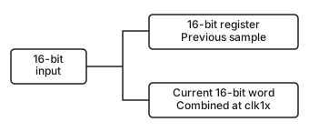
time-division data conversion
wide_to_narrow
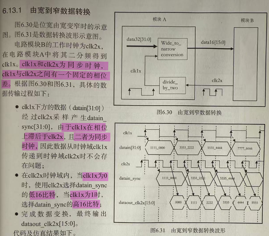
1 | module wide_to_narrow |
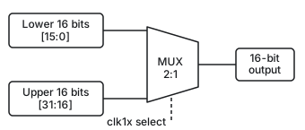
narrow_to_wide
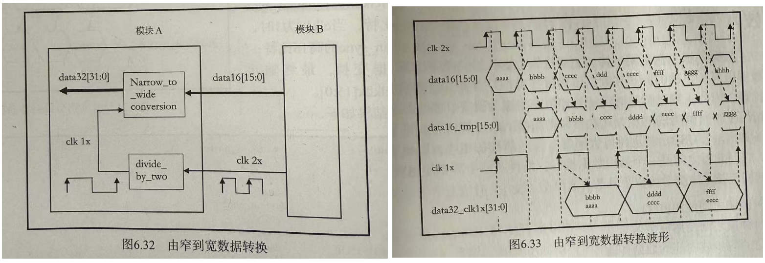
1 | module narrow_to_wide |
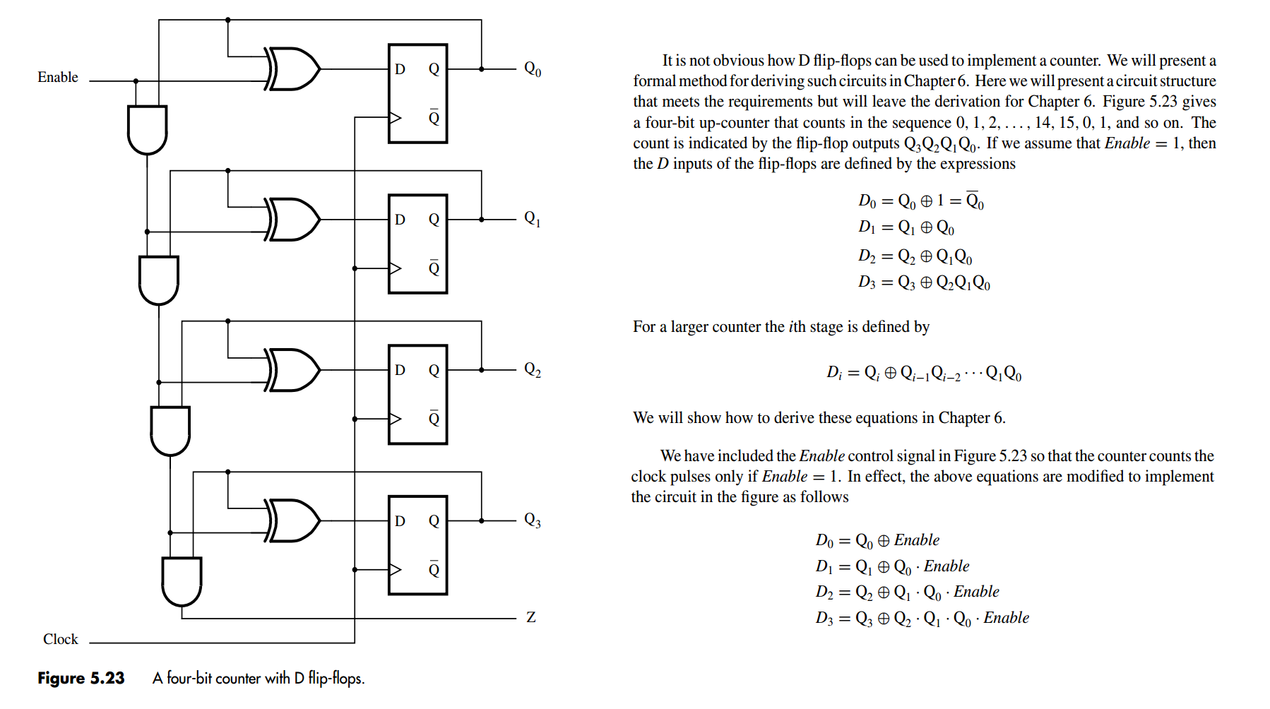
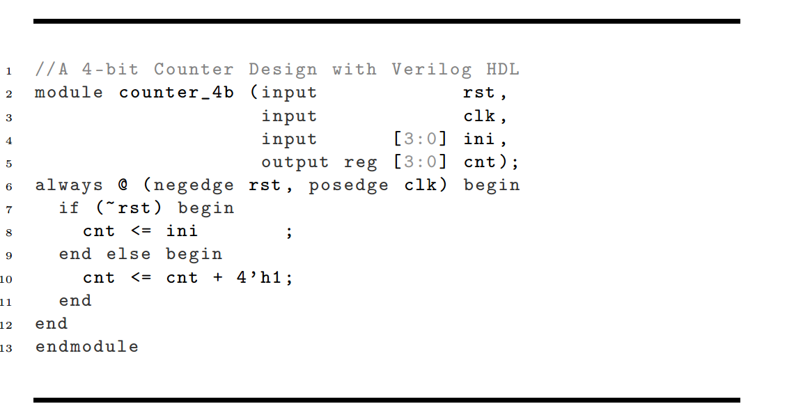
Synchronous Counter with D Flip-Flops
Ring-Counter,Johnson-Counter [https://igulms.iqdigit.com/storage/15810/Ring-Counter,Johnson-Counter.pdf]
counter as FSM
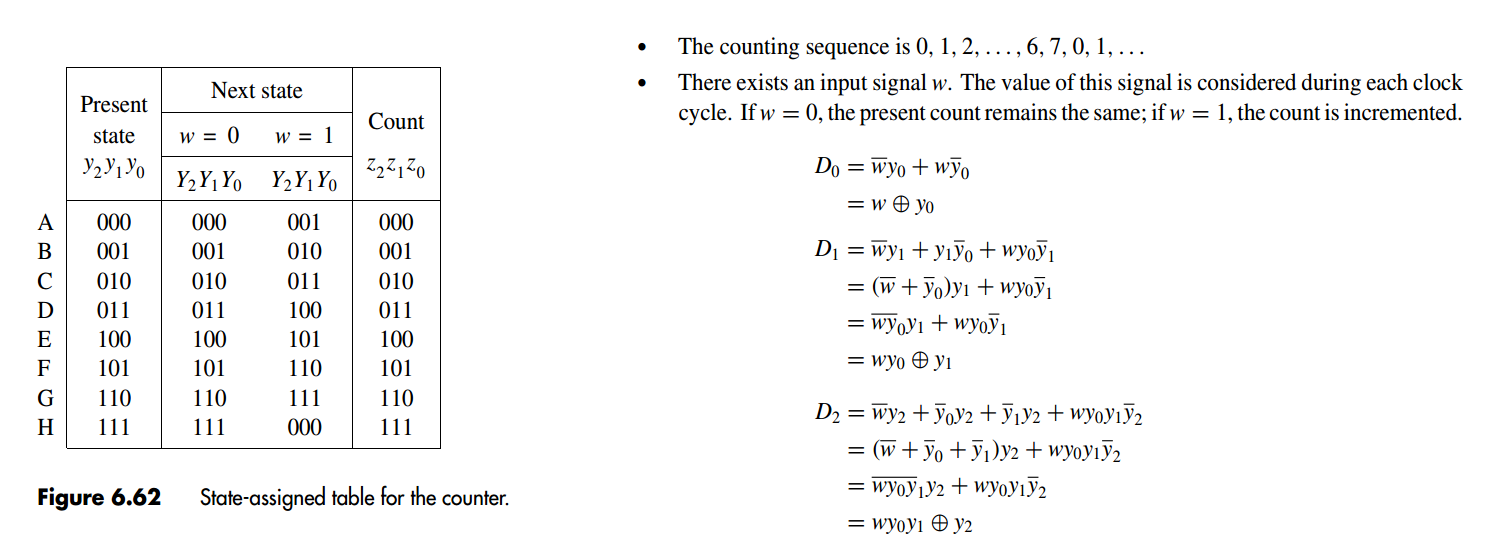
ring counter, a.k.a. one-hot counter
connects the output of the last shift register to the first shift register input and circulates a single one (or zero) bit around the ring
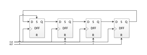
If \(N\) flip-flop are there, then it counts \(\color{red}N\) states
Johnson counter, a.k.a. twisted ring counter
connects the last shift register's complemented output to the input of the first register and circulates a stream of ones followed by zeros around the ring
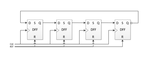
If \(N\) flip-flop are there, then it counts \(\color{red}2N\) states
MASH 1-1-1 in DSP
MASH-1-1-1 Noise-Shaping Truncator (DLF → DAC) [https://github.com/raytroop/dsmwk]
Digital block between a 20-bit digital loop filter (DLF) output and an 8-bit DAC input. The 12 truncated LSBs are pushed through a MASH-1-1-1 delta-sigma modulator so the truncation error is 3rd-order noise-shaped instead of lost:
1 | dac(z) = dlf(z)/2^12 - (1 - z^-1)^3 · q(z) (× z^-1 latency) |
where e3 is the stage-3 accumulator residue in raw
20-bit-LSB counts (0…4095, quantizer step 2¹²) and q is the
same error referred to the 8-bit output grid — the unit-step
quantization noise of the effective 1-LSB₈ quantizer.
dac(z) = dlfMSB8 (z)/212 + dlfLSB12 (z)/212+ q(z) · (1 - z-1)3 = dlf(z)/212 + q(z) · (1 - z-1)3
1 | dlf_in[19:12] ─────────────────────────────────┐ |
flowchart LR
    IN["dlf_in<br/>20 bits"] -->|"upper 8 bits"| XMSB["x_msb<br/>coarse value"]
    IN -->|"lower 12 bits"| A1["Stage 1<br/>acc1 + x_frac"]

    R1[("acc1<br/>register")] --> A1
    A1 -->|"residue r1"| R1
    A1 -->|"r1"| A2["Stage 2<br/>acc2 + r1"]
    A1 -->|"carry c1"| NC["Noise cancellation<br/>c1 + c2 − c2_d1<br/>+ c3 − 2c3_d1 + c3_d2"]

    R2[("acc2<br/>register")] --> A2
    A2 -->|"residue r2"| R2
    A2 -->|"r2"| A3["Stage 3<br/>acc3 + r2"]
    A2 -->|"carry c2"| NC
    A2 -->|"c2"| C2D1[("c2_d1<br/>z⁻¹")]
    C2D1 -->|"−c2_d1"| NC

    R3[("acc3<br/>register")] --> A3
    A3 -->|"residue r3"| R3
    A3 -->|"carry c3"| NC
    A3 -->|"c3"| C3D1[("c3_d1<br/>z⁻¹")]
    C3D1 -->|"−2c3_d1"| NC
    C3D1 --> C3D2[("c3_d2<br/>z⁻²")]
    C3D2 -->|"+c3_d2"| NC

    NC -->|"signed correction y<br/>−3…+4"| ADD["x_msb + y"]
    XMSB --> ADD
    ADD --> SAT["Clamp to 0…255"]
    SAT --> OUTREG[("Output register")]
OUTREG --> OUT["dac_out<br/>8 bits"]| Branch | Expression | Range |
|---|---|---|
| stage 1 | c1 |
{0, 1} |
| stage 2 | (1−z⁻¹)·c2 = c2 − c2_d1 |
{−1, 0, +1} |
| stage 3 | (1−z⁻¹)²·c3 = c3 − 2·c3_d1 + c3_d2 |
[−2, +2] |
| total | y |
[−3, +4] |
1 | wire signed [5:0] y = |
Each carry is a bare bit {0,1}. {5'b0, c1}
zero-extends it to 6 bits (value unchanged), and
$signed(...) marks it for signed arithmetic. The term
{4'b0, c3_d1, 1'b0} is c3_d1 with a zero
appended — a shift-left-by-1, i.e. 2·c3_d1 (value 0 or 2) —
so the multiply costs nothing.
The reachable values of y and their actual bit
patterns:
| value | y[5:0] |
value | y[5:0] |
|
|---|---|---|---|---|
| +4 | 000100 |
0 | 000000 |
|
| +3 | 000011 |
−1 | 111111 |
|
| +2 | 000010 |
−2 | 111110 |
|
| +1 | 000001 |
−3 | 111101 |
Worked example:
c1=0, c2=0, c2_d1=1, c3=0, c3_d1=1, c3_d2=0 →
y = 0 + (0−1) + (0−2+0) = −3 → 111101.
clamp [-3, 259] to [0, 255]
For msb ∈ [3, 251], x_msb + y never leaves
[0,255], the mux always takes the pass-through leg, and
dac_sat ≡ dac_sum bit-for-bit.
1 | //------------------------------------------------------------------------- |
In a locked PLL the DLF integrator sits mid-range and the clamp never fires — cost: zero. It engages only during acquisition/slew, where noise is irrelevant and its job is exactly right: drive the DAC monotonically to the rail without wrapping
overall ENOB calculation
1 | SNR = P_sig / (P_q,in + P_dsm) (powers add — sources are independent) |
with everything in the same units (LSB₈² is convenient) and — critically — both noise terms integrated in-band only (0 … f_bw, i.e. what survives the analog filter):
| Term | Expression (LSB₈², fs = f_clk) |
|---|---|
| Signal (full-scale sine convention) | P_sig = FS²/8 = 256²/8 = 8192 |
| DSM shaped noise, in-band | P_dsm = (1/12)·(π⁶/7)·OSR⁻⁷ |
| Input quantization noise, in-band | P_q,in = (2⁻¹²)²/12 · κ |
Sanity check at OSR = 50 (static input, κ=1):
P_q,in = 4.97e-9, P_dsm = 1.47e-11 → SNR =
122.1 dB → ENOB = 19.98 — the DSM costs only 0.13 dB
against the ideal 20.00. At OSR = 10: DSM dominates, ENOB = 16.1
RTL module
Wei Yet, MakerCode RTL Challenge [https://github.com/Weiyet/MakerCode_RTLChallenge]
decimation_filter
Filter Equation
1 | filtered[n] = (1*x[n] + 3*x[n-1] + 3*x[n-2] + 1*x[n-3]) / 8 |
1 | iverilog -g2012 -o sim.vvp solution.sv tb.sv |
1 | module decimation_filter #( |
Line 34 uses non-blocking assignment:
1 | x1 <= data_in; // line 34: scheduled, NOT applied yet |
Non-blocking assignments don't take effect until the end of the current time step (after all the blocking statements in the block have run). So at line 37:
x1still holds its previous value — i.e. the sample from the lastdata_valid_incycle, which isx[n-1].data_inis the current sample,x[n].
They are different values. That's deliberate and necessary for the FIR math to be correct:
1 | filtered = 1*x[n] + 3*x[n-1] + 3*x[n-2] + 1*x[n-3] |
| Symbol | Value at line 37 | Filter tap |
|---|---|---|
data_in |
x[n] (current) | coeff 1 |
x1 |
x[n-1] | coeff 3 |
x2 |
x[n-2] | coeff 3 |
x3 |
x[n-3] | coeff 1 |

gray-code
1 | function automatic logic [3:0] bin2gray(input logic [3:0] bin); |
1 | function automatic logic [3:0] bin2gray(input logic [3:0] bin); |
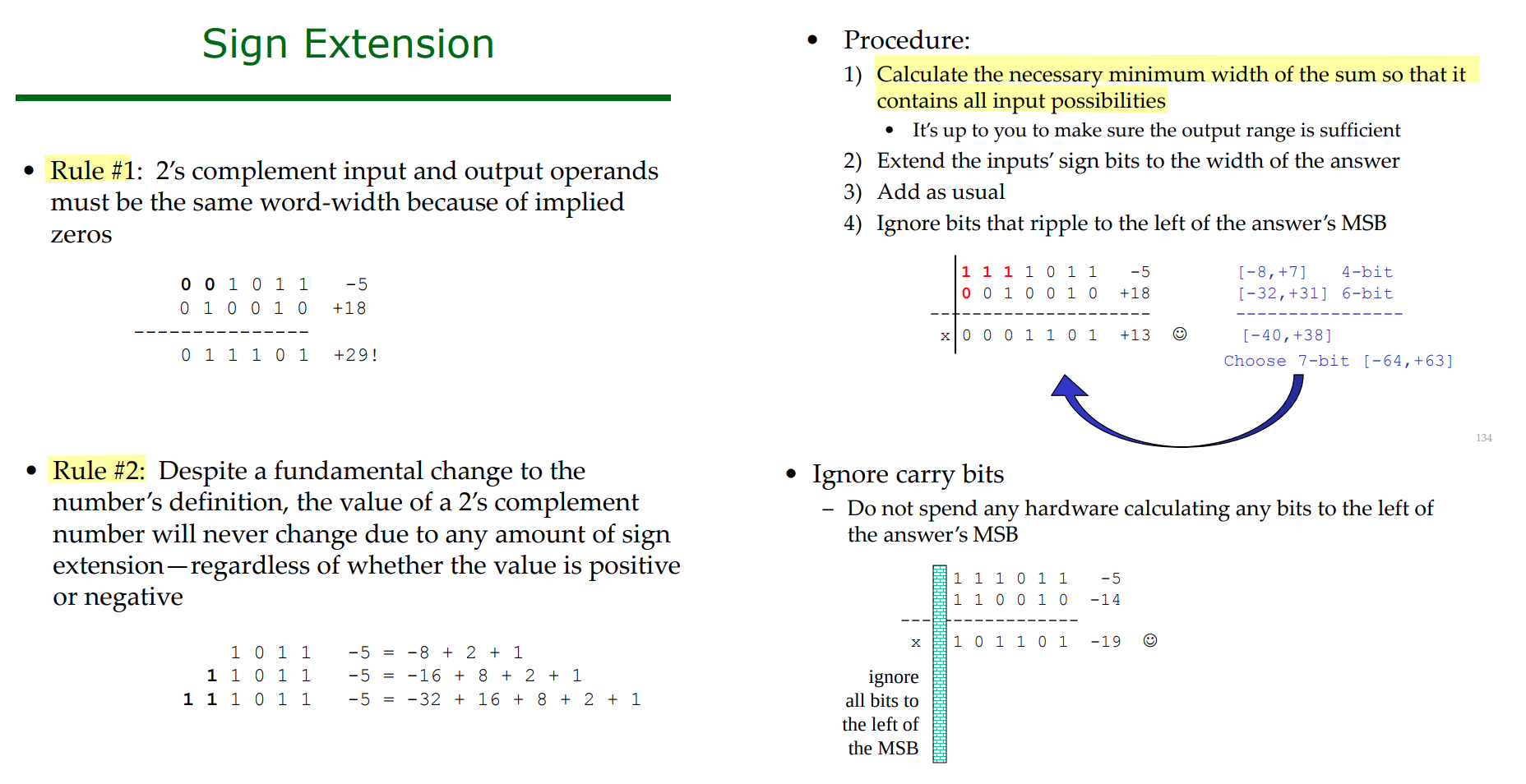
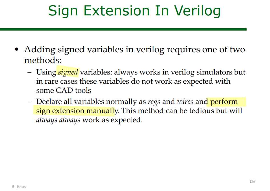
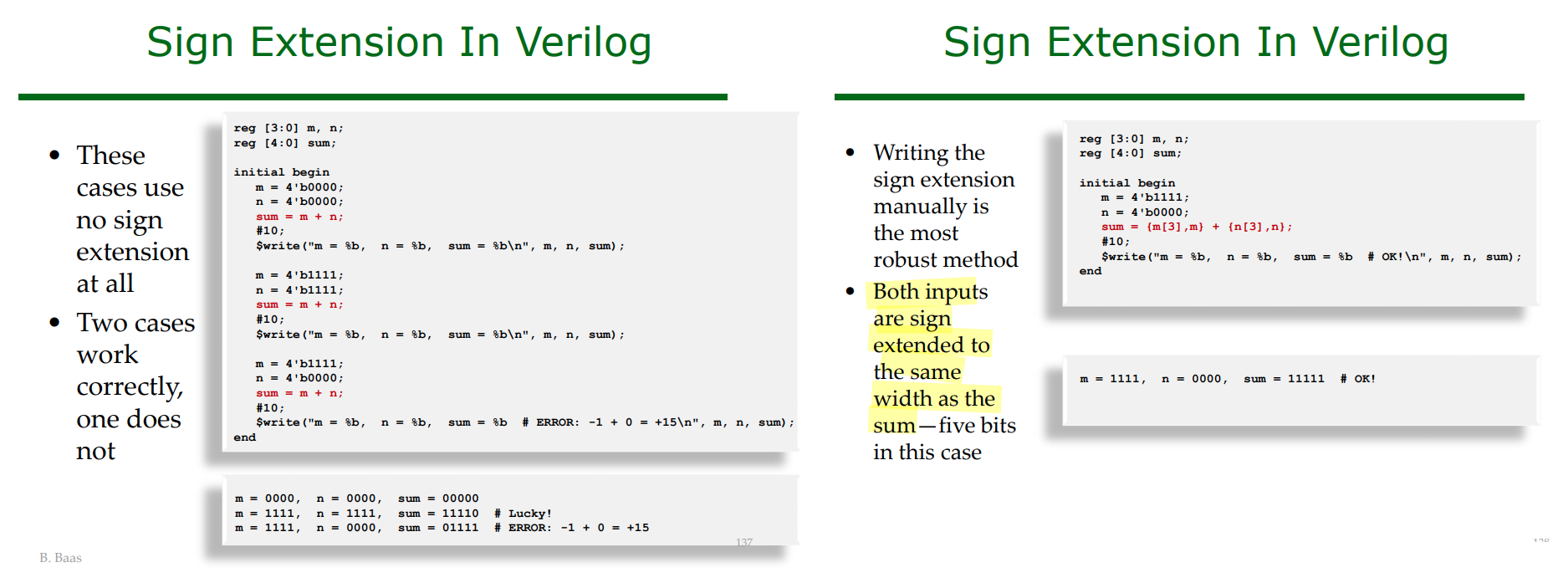
Sign Extension In Verilog
[https://www.ece.ucdavis.edu/~bbaas/281/notes/Handout.sign.extension.pdf]
reference
K. K. Mishra, Advanced Chip Design: Practical Examples in Verilog. CreateSpace Independent Publishing Platform, 2013
Brown, Stephen, and Zvonko Vranesic. Fundamentals of Digital Logic with Verilog Design. 3rd ed., McGraw-Hill Higher Education, 2014. [https://daskalakispiros.com/files/Ebooks/Fundamentals_of_Digital_Logic_with_Verilog_Design_(3rd_edition)__ebook3000.pdf]
X. Yang, Integrated Circuit Design: IC Design Flow and Project-Based Learning, 1st edition. Boca Raton: CRC Press, 2024
Wei Yet, MakerCode RTL Challenge [https://github.com/Weiyet/MakerCode_RTLChallenge]
Bevan Baas, EEC281 VLSI Digital Signal Processing, [https://www.ece.ucdavis.edu/~bbaas/281/]
Mark Horowitz. EE371: Advanced VLSI Circuit Design Spring 2006-2007 [https://web.stanford.edu/class/archive/ee/ee371/ee371.1066/]
Tinoosh Mohsenin. CMPE 691: Digital Signal Processing Hardware Implementation [https://userpages.cs.umbc.edu/tinoosh/cmpe691/]
Keshab K. Parhi [http://www.ece.umn.edu/users/parhi/]
謝秉璇. 2019 積體電路設計導論 [link]
E-Hung Chen, MTK, ISSCC 2026 Forum F2.3: State-of-the-Art 200+ Gb/s Electrical and Optical Interconnects
G. Kim et al., "Parallel Implementation Technique of Digital Equalizer for Ultra-High-Speed Wireline Receiver," 2018 IEEE International Symposium on Circuits and Systems (ISCAS), Florence, Italy, 2018, pp. 1-5 [https://sci-hub.ru/10.1109/ISCAS.2018.8350924]