While JTAG connects chips externally, IJTAG
extends it inside the chip — linking embedded instruments (MBIST,
sensors, monitors, etc.) through a reconfigurable network.
Pin-Mux Logic Pins are precious in SoC
design!
Pin-Mux Logic lets functional and test signals share the same pins
depending on the mode.
During test mode, JTAG/IJTAG signals are routed internally via
multiplexers — saving pins and silicon area.
Basic idea: use of mean of \(v'(t)\) to approximate
median of \(v'(t)\)
Elmore delay approximates the median of \(h(t)\) by the mean of
\(h(t)\)
Distributed RC-Line
Lumped approximations
\(rc\)-models
If your simulator does not support a distributed \(rc\)-model, or if the computational
complexity of these models slows down your simulation too much, you can
construct a simple yet accurate model yourself by approximating the
distributed \(rc\) by a lumped RC
network with a limited number of elements
The accuracy of the model is determined by the number of stages. For
instance, the error of the \(\Pi -3\)
model is less than 3%, which is generally sufficient.
Why use "\(\Pi\)
Model"
examples
Wire Inductive Effect
RC delay increases quadratically with length
LC delay (speed of light flight time) increases linearly with
length
Inductance will only be important to the delay of low-resistance
signals such as wide clock lines
wave
Signal propagates over the wire as a wave (rather
than diffusing as in \(rc\) only models)
Signal propagates by alternately transferring energy from capacitive
to inductive modes
A glitch is an unwanted pulse at the output of a
combinational logic network – a momentary change in an
output that should not have changed
A circuit with the potential for a glitch is said to have a
hazard
In other words a hazard is something intrinsic about a circuit; a
circuit with hazard may or may not have a glitch depending on input
patterns and the electric characteristics of the circuit.
When do circuits have hazards
?
Hazards are potential unwanted transients that occur in the output
when different paths from input to output have different propagation
delays
Isolation cells are additional cells
inserted by the synthesis tools for isolating the buses/wires crossing
from power-gated domain of a circuit to its always-on
domain (AON).
To prevent corruption of always-on domain, we clamp the nets crossing
the power domains to a value depending upon the design.
A simple circuit having a switchable (or gated) power
domain
The circuit shown in Figure 1, after isolation cells are
inserted
Clock Gating is defined as: "Clock gating is a
technique/methodology to turn off the clock to certain parts of the
digital design when not needed".
AND gate-based clock gating
In simplest form a clock gating can be achieved by using an
AND gate as shown in picture below
However, this simplest form of clock gating technique has some
problem of generating glitches in the clock provide to
the FF, which are not desirable.
Glitches in enable/gated clock
Latch based clock gating
These glitches can be removed by introducing a negative edge
triggered FF (assuming downstream FFs are positive edge) or low-level
sensitive latch at the output of the clock enable signal.
This will make sure that any glitch in the clock enable signal will
not be visible to the gated clock output. The Latch output will only be
updated during the negative clock cycle and thus input to AND gate will
be stable high.
Glitch Free Gated Clock
OCV Derating With AOCV
Genus Attribute Reference 22.1
Innovus Text Command Reference 22.10
Article (20416394) Title: Analysis with Advanced On-chip Variation
(AOCV) derating in EDI system and ETS
When set to aocv_multiplicative, the derating factor
will be calculated as AOCV derating * OCV derating, which is set using
the set_timing_derate command.
When set to aocv_additive, the derating factor will be
calculated as AOCV derating + OCV derating values.
When you use this global variable, the report_timing
command shows the total_derate column in the timing report
output, which allows you to view and cross-check the calculated total
derate factor.
To set this global variable, use the set_global
command.
Gildenblat, G. S. (2010). Compact modeling : principles, techniques
and applications. Springer.
VDS Effect On Channel Noise
\[
\color{red} \overline{i^2_d} \propto V_{DS}
\]
K. Ohmori and S. Amakawa, "Direct White Noise Characterization of
Short-Channel MOSFETs," in IEEE Transactions on Electron
Devices, vol. 68, no. 4, pp. 1478-1482, April 2021 [pdf,
slides]
X. Ding, G. Niu, A. Zhang, W. Cai and K. Imura, "Experimental
Extraction of Thermal Noise γ Factors in a 14-nm RF FinFET technology,"
2021 IEEE 20th Topical Meeting on Silicon Monolithic Integrated
Circuits in RF Systems (SiRF), San Diego, CA, USA, 2021[https://sci-hub.se/10.1109/SiRF51851.2021.9383331]
NF50
TODO 📅
\(\gamma\) vs VDS, VGS in simulation
N28
fix VDS, sweep VGS
fix VGS, sweep VDS
MOS Flicker Noise
T. Noulis, "CMOS process transient noise simulation analysis and
benchmarking," 2016 26th International Workshop on Power and Timing
Modeling, Optimization and Simulation (PATMOS), Bremen, Germany, 2016
[https://sci-hub.ru/10.1109/PATMOS.2016.7833428]
Above simulation demonstrate that flicker noise is
represented by a drain-source current in BSIM
model, however modeled as a voltage source in series with the gate
is just for calculating convenience
⭐ where \(S_{x_n}^T=\frac{\partial
T}{\partial x_n}\frac{x_n}{T}\) is relative
sensitivity
relative sensitivity connect \(\frac{dx_n}{x_n}\) with total relative
variation \(\frac{dT}{T}\)
And \(dT\) can be expressed as \[
dT =\sum_{n=1}^N S_{x_n}^T T\cdot \frac{dx_n}{x_n} = \sum_{n=1}^N
x_n'\cdot \frac{dx_n}{x_n}
\] ⭐ where \(x_n'= S_{x_n}^T
T\) is the contribution of \(x_n\) in \(T\)
⭐ For parallel or series resistors, it can prove \(\sum_{n=1}^N S_{x_n}^T = 1\) and \(\sum_{n=1}^N x_n'=T\)
Here \(T= R_1 \parallel R_2 =
\frac{R_1R_2}{R_1+R_2}\), and \(T|_{R_1=8000, R_2=2000} = 1600\)
The contribution of \(R_1\) and
\(R_2\) to \(T\)\[\begin{align}
R_1' &= S_{R_1}^T T | _{R_1=8000, R_2=2000} = 320 \\
R_2' &= S_{R_2}^T T | _{R_1=8000, R_2=2000} = 1280
\end{align}\]
If \(V_{DS}\) is slightly
greater than \(V_{GS} - V_{TH}\), then
the inversion layer stops at \(x \leq
L\), and we say the channel is "pinched
off"
Upon passing the pinchoff point, the electrons simply shoot through
the depletion region near the drain junction and arrive at the drain
terminal
\(L^{'}\) is the function of
\(V_{DS}\)
with \(\frac{1}{L^{'}} =
\frac{1}{L-\Delta L}=\frac{L+\Delta L}{L^2-\Delta L^2}\approx
\frac{1}{L}\left(1+\frac{\Delta L}{L}\right)\), we have \[
I_D \approx \frac{1}{2}\mu_n C_{ox}\frac{W}{L}\left(1+\frac{\Delta
L}{L}\right)(V_{GS}-V_{TH})^2 = \frac{1}{2}\mu_n
C_{ox}\frac{W}{L}(V_{GS}-V_{TH})^2 (1+\lambda V_{DS})
\] assuming \(\frac{\Delta L}{L} =
\lambda V_{DS}\)
\(\lambda\) represents the
relative variation in length for a given increment in \(V_{DS}\). Thus, for longer channels, \(\lambda\) is smaller
In reality, however, \(r_O\) varies
with \(V_{DS}\). As \(V_{DS}\)increases and the
pinch-off point moves toward the source, the rate at which the
depletion region around the source becomes wider decreases,
resulting in a higher incremental output impedance.
The dependence of offset voltage and current mismatches upon the
overdrive voltage is similar to our observations for corresponding
noise quantities
differential pair
In reality, since mismatches are independent statistical
variables
Above shows that the input transistors must be designed for high
gain (\(g_mr_o =
\frac{2}{V_{OV}\lambda}\)), which means they must be designed for
small\(V_{GS}-V_{TH}\).
It is desirable to minimize \(V_{GS}-V_{TH}\) by lowering the tail
current or increasing the transistor widths
M. Tian, V. Visvanathan, J. Hantgan and K. Kundert, "Striving for
small-signal stability," in IEEE Circuits and Devices Magazine, vol. 17,
no. 1, pp. 31-41, Jan. 2001 [https://kenkundert.com/docs/cd2001-01.pdf]
Then, we get \[
V_{os}=\frac{V_o'-V_o}{A}+(V_m'-V_m)
\] Due to \(V_o=V_m\) and \(V_o'=V_m'\)\[
V_{os}=(1/A+1)\Delta{V_m}
\] or \[
V_{os}=(1/A+1)\Delta{V_o}
\] if \(A \gg 1\)\[
V_{os}=\Delta{V_o}
\]
we get \[
V_{os}=\frac{V_o'-V_o}{A}+(V_m'-V_m)
\] or \[
V_{os}=\frac{\Delta V_o}{A}+\beta \Delta V_o
\] if \(A \gg 1\)\[
V_{os}=\beta \Delta V_o
\] or \[
V_{os}=\Delta V_m
\]
Lecture 22 Variability and Mismatch of Dr. Hesham A. Omran's
Analog IC Design
There is discrepancy between model operating point and \(V_{ds}/I_{ds}\)
I believe that the equation \(V_{ds}/I_{ds}\) is more appropriate where
mos is used as switch, though \(V_{ds}=0\) is an outlier.
Schmitt Inverter
gm/ID Intuition
small gm/ID for High ro, or high Early voltage \(V_A\)
Transit Frequency \(f_T\)
Defined as the frequency at which the small-signal current
gain of a device is unity
mag(Ids@ft) = Ig(1mA)
Aditya Varma Muppala. MMIC 08: High Frequency Device Characterization
in Cadence - Fmax, Ft, NFmin vs Jd [https://youtu.be/kgEypIA8eus]
ZTC Bias Points
M. Coelho et al., "Is There a ZTC Biasing Point in the
Leading-Edge FET Intrinsic Gain gmrDS?," 2025 9th International
Young Engineers Forum on Electrical and Computer Engineering
(YEF-ECE), Caparica / Lisbon, Portugal, 2025
M. Coelho et al., "Analysis of the ZTC Bias Points in the
FinFET Gate Capacitance and Transition Frequency," 2025 37th
International Conference on Microelectronics (ICM), Cairo, Egypt,
2025, pp. 1-6, doi: 10.1109/ICM66518.2025.11322461
there's a specific bias point where the MOSFET transition frequency
(fT) becomes almost temperature‑independent
MOM cap of wo_mx
Monte Carlo model:
\(C_{pa}=C_{pa1}\), \(C_{pb}=C_{pb1}\) for each iteration during
Process Variation
different variation is applied to \(C_{ab}\) and \(C_{a1b1}\) each iteration during
Mismatch Variation, though \(C_{pa}\), \(C_{pb}\), \(C_{pa1}\) and \(C_{pb1}\) remain constant
\(C_\text{eq}\) and \(R_\text{eq}\) are obtained \[\begin{align}
C_\text{eq} &= \frac{1+|A|^2-2A_r}{1-A_r}\cdot C_f \\
R_\text{eq} &= \frac{A_i}{1+|A|^2-2A_r}\cdot \frac{1}{\omega C_f}
\end{align}\]
D/S small signal model
The Drain and Source of MOS are determined
in DC operating point, i.e. large signal.
That is, top of \(M_2\) is
drain and bottom is source, \[\begin{align}
R_\text{eq2} &= \frac{r_\text{o2}+R_L}{1+g_\text{m2}r_\text{o2}} \\
& \simeq \frac{1}{g_\text{m2}}
\end{align}\]
PMOS small signal model
polarity
The small-signal models of NMOS and PMOS transistors are
identical
A negative \(\Delta V_\text{GS}\)
leads to a negative \(\Delta I_D\).
Recall that \(I_D\), in the
direction shown here, is negative because the actual current of holes
flows from the source to the drain.
Conversely, a positive \(\Delta
V_\text{GS}\) produces a positive \(\Delta I_D\), as is the case for an NMOS
device.
W. M. Elgharbawy and M. A. Bayoumi, "Leakage sources and possible
solutions in nanometer CMOS technologies," in IEEE Circuits and Systems
Magazine, vol. 5, no. 4, pp. 6-17, Fourth Quarter 2005, doi:
10.1109/MCAS.2005.1550165.
X. Qi et al., "Efficient subthreshold leakage current optimization -
Leakage current optimization and layout migration for 90- and 65- nm
ASIC libraries," in IEEE Circuits and Devices Magazine, vol. 22, no. 5,
pp. 39-47, Sept.-Oct. 2006, doi: 10.1109/MCD.2006.272999.
P. Monsurró, S. Pennisi, G. Scotti and A. Trifiletti, "Exploiting the
Body of MOS Devices for High Performance Analog Design," in IEEE
Circuits and Systems Magazine, vol. 11, no. 4, pp. 8-23, Fourthquarter
2011, doi: 10.1109/MCAS.2011.942751.
Andrea Baschirotto, ISSCC2015 "ADC Design in Scaled Technologies"
As a result of DIBL, threshold voltage is reduced
with shorter channel lengths and, consequently, the subthreshold leakage
current is increased
impact on output impedance
The principal impact of DIBL on circuit design is the degraded output
impedance.
In short-channel devices, as \(V_{DS}\) increases further, drain-induced
barrier lowering becomes significant, reducing the threshold
voltage and increasing the drain current
Impact Ionization and GIDL are different, however both
increase drain current, which flowing from the drain into the
substrate
Gate induced drain leakage
(GIDL)
The large current flows from the drain to bulk and this
drain leakage current is named gate-induced drain leakage
(GIDL) since it is due to a gate-induced high electric
field present in the gate-to-drain overlap region
gate-induced drain leakage (GIDL) increases exponentially due to the
reduced gate oxide thickness
Chauhan, Yogesh Singh, et al. FinFET modeling for IC simulation
and design: using the BSIM-CMG standard. Academic Press, 2015.
\[
\frac{g_m}{I_D} = \frac{2}{V_{GS}-V_{TH}}
\] Decrease of gm/Id results from decrease in VT.
GIDL (Gate induced drain leakage) as at weak
inversion may results in a weak lateral electric field causing leakage
current between drain and bulk, which degrade the efficiency of the
transistor (gm/ID).
In advanced node, gate leakage is also a strong function of
temperature
Power/Ground and I/O Pins
Power / Ground Pin
Information
In both digital and analog I/O, power and ground pins appear at the
sub-circuit definiton, allowing user to use the I/O in voltage islands.
They follow certain naming conventions.
digital I/O sub-circuit
VDD: pre-driver core voltage (supplied by PVDD1CDGM)
VSS: pre-driver ground and also global ground (supplied by
PVDD1CDGM)
VDDPST: I/O post-driver voltage, i.e. 1.8V (supplied by PVDD2CDGM or
PVDD2POCM)
VSSPOST: I/O post-driver ground (supplied by PVDD2CDGM or
PVDD2POCM)
POCCTRL: POCCTRL signal (supplied by PVDD2POCM)
analog I/O placed in a core voltage domain, the convention is
TACVDD: analog core voltage (supplied by PVDD3ACM)
TACVSS: analog core ground (supplied by PVDD3ACM)
VSS: global core ground
analog I/O placed in an I/O voltage domain, the convention is:
TAVDD: analog I/O voltage, i.e. 1.8V (supplied by PVDD3AM)
TAVSS: analog I/O ground (supplied by PVDD3AM)
VSS: global core ground
Power/Ground Combo Cells
power/ground combo pad cell
pins to be connected to bump
to core side pin name
PVDD1CDGM
VDD VSS
VDD VSS
PVDD2CDGM PVDD2POCM
VDDPST VSSPST
N/A
PVDD3AM
TAVDD TAVSS
AVDD AVSS
PVDD3ACM
TACVDD TACVSS
AVDD AVSS
Note for the retention mode
At initial state, IRTE must be 0 when VDD is
off.
IRTE must be kept >= 10us after VDD turns on again (from the
retention mode to the normal operation mode).
IRTE can be switched only when both VDD and VDDPST are on.
When the rention function is needed, IRTE signal must come from an
"always-on" core power domain. If you don't need the rention function,
it is required to tie IRTE to ground. In other words, no matter
the rention feature is needed or not, it is required to have PCBRTE in
each domain.
Note: PCBRTE does not need PAD
connection.
Internal Pins
There are 3 internal global pins, i.e. ESD,
POCCTRL, RTE, in all digital domain
cells.
In real application,
ESD pin is an internal signal and
active in ESD event happening
POCCTRL is an internal signal and active in
Power-on-control event.
However, these special events (i.e. ESD event and Power-on-control
event) are not modeled in NLDM kit (.lib), only normal function is
covered, so ESD and POCCTRL pins are
simply defined as ground in NLDM kit (.lib).
These 3 global pins will be connected automatically after
cell-to-cell abutting in physical layout.
Power-Up sequence in
Digital Domain
Power up the I/O power (VDDPST) first, then the core power (VDD)
PVDDD2POCM cell would generate Power-On-Control signal (POCCTRL) to
have the post-driver NMOS and PMOS off, so that the crowbar current
would not occur in the post-driver fingers when the I/O voltage is on
while the core voltage remains off. As such, I/O cell would be in the
Hi-Z state. when POCCTRL is on, the pll-up/down resistor is disabled and
C is 0.
The POCCTRL signal is transmitted to I/O cells through cell
abutment. There is no need to have routing for POCCTTRL nor
give a control signal to the POCCTRL pin any of I/O cells. Note that the
POCCTRL signal would be cut if inserting a power-cut (PRCUT) cell.
Power-Down sequence in
Digital Domain
It's the reverse of power-up sequence.
Use model in Innovus
1
2
3
4
5
6
7
8
9
10
11
12
set init_gnd_net "vss_core vss DUMMY_ESD DUMMY_POCCTRL"
Ali Sheikholeslami, Circuit Intuitions: Thevenin and Norton
Equivalent Circuits, Part 3 IEEE Solid-State Circuits Magazine, Vol. 10,
Issue 4, pp. 7-8, Fall 2018.
—, Circuit Intuitions: Thevenin and Norton Equivalent Circuits, Part
2 IEEE Solid-State Circuits Magazine, Vol. 10, Issue 3, pp. 7-8, Summer
2018.
—, Circuit Intuitions: Thevenin and Norton Equivalent Circuits, Part
1 IEEE Solid-State Circuits Magazine, Vol. 10, Issue 2, pp. 7-8, Spring
2018.
—, Circuit Intuitions: Miller's Approximation IEEE Solid-State
Circuits Magazine, Vol. 7, Issue 4, pp. 7-8, Fall 2015.
The most accurate method to calculate the degradation of transistors
is the SPICE-level simulation of the whole netlist with application
programming interface (API) and industry-standard stress process
models
MOSRA: MOSFET reliability analysis Synopsys
RelXpert: Cadence
TMI: TSMC Model Interface, TSMC
OMI: Open Model Interface, Si2 standard,
The Silicon Integration Initiative (Si2) Compact Model Coalition has
released the Open Model Interface, an Si2 standard, C-language
application programming interface that supports SPICE compact model
extensions.OMI allows circuit designers to simulate and analyze such
important physical effects as self-heating and aging,
and perform extended design optimizations. It is based on TMI2, the TSMC
Model Interface, which was donated to Si2 by TSMC in 2014.
TDDB: Time-Dependent Dielectric Breakdown
HCI: Hot Carrier injection
BTI: Bias Temperature Instability
NBTI: Negative Bias Temperature Instability
PBTI: Positive Bias Temperature Instability
SHE: Self-Heating Effect
Self-Heating Effect (SHE)
Self-heating effect (SHE) is composed of
FEOL self-heat and BEOL
self-heat, both contribute to the \(\Delta T\)
aging w/i SHE
EM w/i SHE
Junjie Chen, Keqing Ouyang ZTE SANECHIPS. Challenges and Solutions of
PI Signoff for Next Generation Large Scale Chips with TSMC 7nm Process
Technology [pdf]
M. Lofrano et al., "Towards accurate temperature prediction
in BEOL for reliability assessment (Invited)," 2023 IEEE
International Reliability Physics Symposium (IRPS), Monterey, CA,
USA, 2023, pp. 1-7, doi: 10.1109/IRPS48203.2023.10117701
Mitigating Self-Heating
A. Loke, "Short Course: Device and Physical Design Considerations for
Circuits in FinFET Technology," 2020 IEEE International Solid-State
Circuits Conference - (ISSCC), San Francisco, CA, USA, 2020 [pdf]
J. E. Proesel, "Short Course: High-Speed and Mixed-Signal Circuit
Design Techniques in FinFET Technology for Wireline and Optical
Interface Applications," 2020 IEEE International Solid-State
Circuits Conference - (ISSCC), San Francisco, CA, USA, 2020
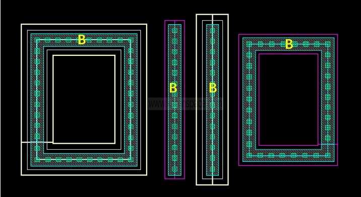
guard ring
closer OD help reduce dT
extended gate
source/drain metal stack
M. Erett et al., "A 0.5–16.3 Gbps Multi-Standard Serial
Transceiver With 219 mW/Channel in 16-nm FinFET," in IEEE Journal of
Solid-State Circuits, vol. 52, no. 7, pp. 1783-1797, July 2017 [https://sci-hub.se/10.1109/JSSC.2017.2702711]
Heat transfer, thermal
resistance
Bias Temperature Instability
(BTI)
BTI occurs predominantly in PMOS (or p-type or p channel)
transistors and causes an increase in the transistor's absolute
threshold voltage.
Stress in the case of NBTI means that the PMOS transistor is
in inversion; that means that its gate to
body potential is substantially below 0 V for analogue circuits
or at VGB = −VDD for digital circuits
Higher voltages and higher temperatures both have
an exponential impact onto the degradation, induced by NBTI.
NBTI will be accelaerated with thinner gate oxide, at a high
temperature and at a high electric field across the oxide region.
During recovery phase where the gate voltage of pMOS is high and
stress is removed, the H atoms in the gate oxiede diffuse back to
Si-SiO2 interface and the recombination of Si-H bonds reduces the
threshold voltage of pMOS.
The net result is an increase in the magnitude of the device
threshold voltage |Vt|, and a degradation of the
channel carrier mobility.
Caution: The aging model provided by fab may
NOT contain recovry effect
Short-channel MOSFETs may exprience high lateral electric
fields if the drain-source voltage is large. while the average
velocity of carriers saturate at high fields, the instantaneous velocity
and hence the kinetic energy of the carriers continue to increase,
especially as they accelerate toward the drain. These are called
hot carriers.
In nanometer technologies, hot carrier effects have
subsided. This is because the energy required to create
an electron-hole pair, \(E_g \simeq 1.12
eV\), is simply not available if the supply voltage is around
1V.
\[
F_E= E \cdot q
\]
\[\begin{align}
E_k &= F_E \cdot s \\
&= E \cdot q \cdot s
\end{align}\]
Electrons and holes gaining high kinetic energies in
the electric field (hot carriers) may be injected into
the gate oxide and cause permanent changes in the
oxide-interface charge distribution, degrading the current-voltage
characteristics of the MOSFET.
The channel hot-electron (CHE) effect is caused by electons flowing
in the channel region, from the source to the drain. This effect is more
pronounced at large drain-to-source voltage, at which the lateral
electric field in the drain end of the channel accelerates the
electrons.
Four different hot carrier injectoin mechanisms can be distinguished:
- channel hot electron (CHE) injection - drain avalanche hot carrier
(DAHC) injection - secondary generated hot electron (SGHE) injection -
substrate hot electron (SHE) injection
HCI is more of a drain-localized mechanism, and is
primarily a carrier mobility degradation (and a Vt
degradation if the device is operated bi-directionally).
For smaller transistor dimensions, CHE dominates the hot
carrier degradation effect
The hot-carrier induced damage in nMOS transistors has been found to
result in either trapping of carriers on defect sites in the oxide or
the creation of interface states at the silicon-oxide interface, or
both.
The damage caused by hot-carrier injection affects the transistor
characteristics by causing a degradation in transconductance, a shift in
the threshold voltage, and a general decrease in the drain current
capability.
HCI seems to have just a weak temperature
dependency
Unlike BTI, it seems to be no or just
little recovery. As holes are much "cooler" (i.e. heavier) than
electrons, the channel hot carrier effect in nMOS devices is shown to be
more significant than in pMOS devices.
Degradation saturation
effect
HCI model can reproduce the saturation effect if stress time is long
enough
K. Yang, R. Zhang, T. Liu, D. -H. Kim and L. Milor, "Optimal
Accelerated Test Regions for Time- Dependent Dielectric Breakdown
Lifetime Parameters Estimation in FinFET Technology," 2018 Conference on
Design of Circuits and Integrated Systems (DCIS), Lyon, France, 2018 [https://par.nsf.gov/servlets/purl/10104486]
Scaling drive more concerns in TDDB
waveform-dependent nature
The figure below illustrates the waveform-dependent nature of these
mechanisms – as described earlier, BTI and HCI depend upon the region of
active device operation. The slew rate of the circuit inputs and output
will have a significant impact upon these mechanisms, especially
HCI.
Negative bias temperature instability (NBTI). This
is caused by constant electric fields degrading the dielectric,
which in turn causes the threshold voltage of the transistor to degrade.
That leads to lower switching speeds. This effect depends on the
activity level of the circuits, with heavier impact on parts of the
design that don’t switch as often, such as gated clocks,
control logic, and reset, programming and test circuitry.
Hot carrier injection (HCI). This is caused by
fast-moving electrons inserting themselves into the gate and
degrading performance. It primarily occurs on higher-voltage modes and
fast switching signals.
longer channel length help both BTI and HCI
larger\(V_{ds}\) help
BTI, but hurt HCI
lower temperature help BTI of core device, but hurt that of
IO device for 7nm FinFET
aging model
MOSRA
MOSRA is a 2-step simulation: 1) Age computation, 2) Post-age
analysis
TMI
BTI recovery effect NOT included for N7
Stochastic Nature
of Reliability Mechanisms
A fraction of devices will fail
Circuit Simulations
Burn-in &
High-temperature operating life (HTOL)
HTOL:
characterization test
characterize the life expectancy
Burn-in:
production test
weed out defective products
HTOL and Burn-in Testing capture the two ends of the reliability
characterization graph known as the "bathtub curve"
Tanya Nigam and Andreas Kerber. Global Foundaries. CICC2014 Session
15 - Challenges for Analog Nanoscale Technologies: Reliability
challenges and modeling of HK MG Technologies
Spectre Tech Tips: Device Aging? Yes, even Silicon wears out -
Analog/Custom Design (Analog/Custom design) - Cadence Blogs - Cadence
Community https://shar.es/afd31p
A. Zhang et al., "Reliability variability simulation methodology for
IC design: An EDA perspective," 2015 IEEE International Electron Devices
Meeting (IEDM), Washington, DC, USA, 2015, pp. 11.5.1-11.5.4, doi:
10.1109/IEDM.2015.7409677.
W. -K. Lee et al., "Unifying self-heating and aging simulations with
TMI2," 2014 International Conference on Simulation of Semiconductor
Processes and Devices (SISPAD), Yokohama, Japan, 2014, pp. 333-336, doi:
10.1109/SISPAD.2014.6931631.
Article (20482350) Title: Measure the Impact of Aging in Spectre
Technology
Karimi, Naghmeh, Thorben Moos and Amir Moradi. “Exploring the Effect
of Device Aging on Static Power Analysis Attacks.” IACR Trans. Cryptogr.
Hardw. Embed. Syst. 2019 (2019): 233-256.[link]
Y. Zhao and Y. Qu, "Impact of Self-Heating Effect on Transistor
Characterization and Reliability Issues in Sub-10 nm Technology Nodes,"
in IEEE Journal of the Electron Devices Society, vol. 7, pp. 829-836,
2019 [https://sci-hub.se/10.1109/JEDS.2019.2911085]
Wafer acceptance testing (WAT) also known as
Process Control Monitoring (PCM)
VT Measurement Methods
A. L. S. Loke, "Constant-Current Threshold Voltage Extraction in
HSPICE for Nanoscake CMOS Analog Design," in Synopsys Users Group
(SNUG) 2010 Conference (San Jose, CA), Mar. 2010. (copyright by AMD) [slides,
paper]
Cu-pillar bumping is a next-generation flip chip interconnection
between chip & packages, especially for fine pitch applications
On the wafer end, comparing to solder bump, cu-pillar bump
provides the advantage of fine pitch; the die size can be reduced about
5~10%.
On the package end, the substrate layer can be reduced from 6
layers to 4 layers by fine pitch and bump on trace process and using
simplified substrate process.
The root cause of the delay mismatch is related to how parasitic
extraction tools distribute coupling capacitances over the nodes of the
resistive networks
The most likely reason for such asymmetry is the anisotropy of
computational geometry algorithms used by extraction tools.
The antenna effect is a common name for the effects
of charge accumulation in isolated nodes of an
integrated circuit during its processing
This effect is also sometimes called "Plasma Induced
Damage", "Process Induced Damage" (PID) or "charging
effect"
This accumulation of charge is usually, and
misleadingly, called the antenna effect.
antenna ratio
During manufacture, if part of the metal wiring is connected to
the gate, but not a diffusion contact, this
"floating" metal collects charge from the plasma.
Manufacturing rules for the antenna effect are usually expressed as
the ratio of the area of floating metal (i.e. charge
collection area) to the area of the gate.
To prevent the antenna effect from destroying your circuit you need
to reduce the floating metal/gate area ratio or give the charge a safe
way to dissipate to the ground before it can build up and cause
damage
metal jumping (bridging,
metal hopping)
Long metal can be taken to higher metal
routing layer, which is known as metal jumping.
This metal jumping is usually done near the gate,
which will mean that there is a full connection to the diffusion contact
before the area of floating metal becomes too large
The jumper is constructed so that the long track is only connected to
the gate once it has also been connected to a diffusion contact, which
then allows the charge to dissipate through diffusion to the
substrate
Diode Insertion
Diode helps dissipate charges accumulated on metal. Diode should be
placed as near as possible to the gate of device on low level of
metal.
In the reverse bias region, the reverse saturation current of Si and
Ge diodes doubles for every \(10 ^oC\)
rise in temperature
pulsic.com, Analog layout – Stop the antenna effect from destroying
your circuit [link]
Prof. Adam Teman, Digital VLSI Design.
Lecture-10-The-Manufacturing-Process [pdf]
In T* DRC deck, it is based on the voltage recognition CAD layer and
net connection to calculate the voltage difference between two
neighboring nets by the following formula:
\[
\Delta V = \max(V_H(\text{net1})-V_L(\text{net2}),
V_H(\text{net2})-V_L(\text{net1}))
\]
where \[
V_H(\text{netx}) = \max(V(\text{netx}))
\] and \[
V_L(\text{netx}) = \min(V(\text{netx}))
\]
The \(\Delta V\) will be
0 if two nets are connected as same potential
If \(V_L \gt V_H\)on a
net, DRC will report warning on this net
Kanamoto, Toshiki, Yasuhiro Ogasahara, Keiko Natsume, Kenji
Yamaguchi, Hiroyuki Amishiro, Tetsuya Watanabe and Masanori Hashimoto.
“Impact of well edge proximity effect on timing.” ESSDERC 2007 -
37th European Solid State Device Research Conference (2007)
J. V. Faricelli, "Layout-dependent proximity effects in deep
nanoscale CMOS," IEEE Custom Integrated Circuits Conference
2010, San Jose, CA, USA, 2010 [https://sci-hub.se/10.1109/CICC.2010.5617407]
LOD is the result of the STI formation (Shallow trench
isolation);
STI becomes compressive as the wafer cools down;
The width of STI (active to active spacing) has a strong impact on
determining stress;
LOD improves holes mobility and decreases electron mobility.
Stress has been more effective for PMOS
This has caused beta (N/P) ratio to fall to about unity at
7nm
LOD effect can be prevented by distancing devices away from the WELL
edge (guard ring). This is usually done by placing dummy devices around
the circuit devices, in which case your circuit devices will also
benefit from the equal edge effects (each device will have the same
neighbours).
Well Proximity Effect (WPE)
Since the well implant dopant (acceptor or donor) is the same type as
the channel implant dopant, the additional doping increases
the absolute value of the threshold voltage (VT) of both NMOS and PMOS
devices
M. Hamaguchi et al., "New layout dependency in high-k/Metal Gate
MOSFETs," 2011 International Electron Devices Meeting, Washington, DC,
USA, 2011 [https://sci-hub.st/10.1109/IEDM.2011.6131614]
Alvin Loke. 2016 VLSI Circuits Short Courses – 2.2 Migrating
Analog/Mixed-Signal Designs to FinFET Alvin Loke / Qualcomm [pdf]
Gate = (ALD MG stack to set \(\Phi_M\))+(metal fill to reduce RG)
Interdigitation provides good matching
properties against 1D-gradients and is
suitable for the simple circuits
The main concept is that you should create an
imaginary center line and place your devices symmetrically, relative to
this line. The simplest example of that is so called
"ABBA" pattern
Interdigitation reduces the device mismatch as it suffers
equally from process variations in X dimension. This technique
was used to layout current mirrors and resistors in PTAT and BGR
circuits.
Common Centroid
Common Centroid provides better matching
for 2D gradients, which is critical for the
large arrays and advanced (below 28nm) nodes
The main idea behind common centroid is that we make our array
symmetrical of the common centre. In other words, the array should be
symmetrical in both X- and Y- axes
The common centroid technique describes that if there are n
blocks which are to be matched then the blocks are arranged
symmetrically around the common centre at equal distances from the
centre. This technique offers best matching for devices as it helps in
avoiding cross-chip gradients
In CNOD, the diffusion is not broken at all. The fabrication process
continues normally, but when standard cells need to be separated, the
gate between them is designated as a dummy gate. This dummy gate is then
connected to a Gate Tie-Down Via to the power rail
This dummy gate tie-down method of CNOD achieves the same horizontal
width savings as SDB, and has the advantage of keeping the
transistor diffusion unbroken and thus can achieve more uniform strain
and performance characteristics
S. Badel et al., "Chip Variability Mitigation through Continuous
Diffusion Enabled by EUV and Self-Aligned Gate Contact," 2018 14th IEEE
International Conference on Solid-State and Integrated Circuit
Technology (ICSICT), Qingdao, China, 2018 [https://sci-hub.st/10.1109/ICSICT.2018.8565694]
4T MPODE (with source/drain) may be formed in
CNOD design layout
potential leakage: channel leakage (S to D);
junction leakage (S/D to bulk)
CNOD (MPODE) is same with primitive
MOS model; PODE is the primitive MOS, just S/D shorted
together
Contacted-Poly-Pitch (CPP)
Wider Contacted-Poly-Pitch allows wider MD and VD size, which help
reduce MEOL IRdrop
Naoto Horiguchi. Entering the Nanosheet Transistor Era [link]
As shown in Fig. 35 in older planar technology nodes, gate pitch is
so relaxed such that S/D contacts and gate contacts can easily be placed
next to each other without causing any shorting risk (see Fig.
35(a)).
As the gate pitch scales, there’s no room to put gate
contacts next to S/D contacts, and gatecontacts have been pushed away
from the active region and are only placed on the STI
region.
In addition, at tight gate pitch, even forming S/D contact
without shorting to gate metal becomes very challenging.
The idea of self-aligned contacts (SAC) has been
introduced to mitigate the issue of S/D contact to gate shorts.
As shown in Fig. 35(b), the gate metal is fully encapsulated by a
dielectric spacer and gate cap, which protects the gate from
shorting to the S/D contact.
A dielectric cap is added on top of the gate so that if the contact
overlaps the gate, no short occurs.
MD layer represent SACs in PDK
self-aligned gate contacts
(SAGCs)
Self-aligned gate contacts (SAGCs) have also been
implemented and Denser standard cells can be achieved by eliminating the
need to land contacts on the gate outside the active area.
SAGCs require the source/drain contacts to be capped with an
insulator that is different from both contact and gate cap dielectrics
to protect the source/drain contacts against a misaligned gate contact
etch.
According to the DRC of T foundary, poly extension > 0 um and
space between MP and OD > 0 um., which demonstrate self-aligned gate
contact is not introduced.
A native layer (NT_N) is usually added under
inductors or transformers in the nanoscale CMOS to define the non-doped
high-resistance region of substrate, which decreases eddy currents in
the substrate thus maintaining high Q of the coils.
For T* PDK offered inductor, a native substrate region is created
under the inductor coil to minimize eddy currents
OD inside NT_N only can be used for NT_N potential pickup purpose,
such as the guarding-ring of MOM and inductor
Derived Geometries
Term
Definition
PW
{NOT NW}
N+OD
{NP AND OD}
P+OD
{PP AND OD}
GATE
{PO AND OD}
TrGATE
{GATE NOT PODE_GATE}
NP: N+ Source/Drain Ion Implantation
PP: P+ Source/Drain Ion Implantation
OD: Gate Oxide and Diffustion
NW: N-WELL
PW: P-WELL
CMOS Processing Technology
Four main CMOS technologies:
n-well process
p-well process
twin-tub process
silicon on insulator
Triple well, Deep N-Well (optional):
NWell: NMOS svt, lvt, ulvt ...
PWell: PMOS svt, lvt, ulvt ...
DNW: For isolating P-Well from the substrate
The NT_N drawn layer adds no process cost and
no extra mask
The N-well / P-well technology, where n-type diffusion is done over a
p-type substrate or p-type diffusion is done over n-type substrate
respectively.
The Twin well technology, where NMOS and
PMOS transistor are developed over the wafer by simultaneous
diffusion over an epitaxial growth base, rather than a substrate.
Deep N-well
Chew, K.W., Zhang, J., Shao, K., Loh, W., & Chu, S.F. (2002).
Impact of Deep N-well Implantation on Substrate Noise Coupling and RF
Transistor Performance for Systems-on-a-Chip Integration. 32nd European
Solid-State Device Research Conference, 251-254. URL:[slides,
paper]
Kuo-Tsai LiPaul ChangAndy Chang, TSMC, US20120053923A1, "Methods of
designing integrated circuits and systems thereof"
Substrate noise
A variety of techniques can be used to minimize this noise, for
example by keeping analog devices surrounded by guard rings, or using a
separate supply for the substrate/well taps.
However guard rings alone cannot prevent noise coupling deep in
the substrate, only surface currents.
PMOS are less noisy than NMOS since PMOS has its nwell which isolates
the substrate noise, but such is not valid for NMOS .
DNW
The N-channel devices built directly into the P-type substrate are
not as effectively isolated as P-channel devices in their N-wells. This
is because despite creating a P+ guard ring around the devices, there
remains an electrical path below the guard ring for charge to flow.
To overcome this issue, a deep N-well can be used to more
effectively isolate these N-channel devices.
the P-well is separated, allowing the voltage to be controlled
because the circuit within the deep N-well is separated from the
p-substrate in this structure, there is the benefit that this circuitry
is less susceptible to noise that propagates through the
p-substrate.
add MIMCAP dummy in chip level due to RV
(Mtop to AP) impact
Track Height of Standard
Cell
Cheng, Chung-Kuan, Byeonggon Kang, Bill Lin and Yucheng Wang.
“Invited: Scaling Standard Cell Layout Using Track Height Compression
and Design Technology Co-optimization.” Proceedings of the 2025
International Symposium on Physical Design (2025) [https://ispd.cc/ispd2026/slides/2025/protected/2_2_slides.pdf]
JED Hurwitz, ISSCC2011 "T4: Layout: The other half of Nanometer CMOS
Analog Design" [slides,
transcript]
Tom Quan, TSMC, Bob Lefferts, Fred Sendig, Synopsys, Custom Design
with FinFETs - Best practices designing mixed-signal IP
Jacob, Ajey & Xie, Ruilong & Sung, Min & Liebmann, Lars
& Lee, Rinus & Taylor, Bill. (2017). Scaling Challenges for
Advanced CMOS Devices. International Journal of High Speed Electronics
and Systems. 26. 1740001. 10.1142/S0129156417400018.
Joddy Wang, Synopsys "FinFET
SPICE Modeling" Modeling of Systems and Parameter Extraction Working
Group 8th International MOS-AK Workshop (co-located with the IEDM
Conference and CMC Meeting) Washington DC, December 9 2015
A. L. S. Loke et al., "Analog/mixed-signal design challenges in 7-nm
CMOS and beyond," 2018 IEEE Custom Integrated Circuits Conference
(CICC), San Diego, CA, USA, 2018, pp. 1-8, doi:
10.1109/CICC.2018.8357060.[slides]
Prof. Adam Teman, Advanced Process Technologies, [pdf]
Luke Collins. FinFET variability issues challenge advantages of new
process [link]
Loke, Alvin. (2020). FinFET technology considerations for circuit
design (invited short course). BCICTS 2020 Monterey, CA
Alvin Leng Sun Loke, TSMC. Device and Physical Design Considerations
for Circuits in FinFET Technology", ISSCC 2020
A. L. S. Loke, C. K. Lee and B. M. Leary, "Nanoscale CMOS
Implications on Analog/Mixed-Signal Design," 2019 IEEE Custom Integrated
Circuits Conference (CICC), Austin, TX, USA, 2019, pp. 1-57, doi:
10.1109/CICC.2019.8780267.
A. L. S. Loke, Migrating Analog/Mixed-Signal Designs to FinFET Alvin
Loke / Qualcomm. 2016 Symposia on VLSI Technology and Circuits
Lattice Semiconductor, 16FFC Process Technology Introduction December
9th, 2021[pdf]
Though it is assumed that \(V_{BE}\)
is a linear function of temperature for first oder analysis.
In practice, \(V_{BE}\) is
slightly nonlinear, the magnitude of this nonlinearity is
referred to as curvature.
curvature depends on the temperature dependency of
the saturation current (\(I_s\)), and on that of the collector
current (\(I_c\)), it can be
written as \[
V_{curv}(T)=\frac{k}{q}(\eta-\delta)(T-T_r-T\cdot \ln(\frac{T}{T_r}))
\] where \(\eta\) = a constant
depending on the doping level, CMOS substrate pnp transistors have a
typically value of \(\eta \cong 4\)
\(\delta\) = order of the
temperature dependence of collector current (\(I_c\))
PTAT \(I_c\) help reduce \(V_{curv}(T)\), \(\delta=1\)
Although the temperature dependence of the bias current \(I_b\) doesn’t impact the accuracy of \(V_{BE}\), it does impact the systematic
nonlinearity or curvature of \(V_{BE}\), and hence the sensor's
systematic error. The curvature in \(V_{BE}\) can be reduced by using a PTAT
bias current.
PTAT bias current
\[
I_{bias} = \frac{0.7}{\beta \cdot R^2}
\] in which \(\beta=\frac{\mu_{n}\cdot
C_{ox}\cdot W}{L}\), where:
\(\mu_n\)=mobility,
\(C_{ox}\) = oxide capacitance
density,
\(\frac{W}{L}\) = dimension ratio of
unit NMOS used for \(M_1\) and \(M_2\)
\(\mu_n\) is complementary
to the absolute temperature and resitor R is implemented using
high-R flow in FinFET which has a low temperature dependency, the net
temperature dependency of \(I_{bias}\)
is proportional to the absolute temperature \[
I_{bias}\propto T
\]
Kamath, Umanath Ramachandra. "BJT Based Precision Voltage Reference
in FinFET Technology." (2021).
Errors due to V-I Finite
Gain
Finite gain introduces errors both in the V-I converters, finite loop
gain results in errors in the closed-loop transconductances.
Then, \(\alpha\) is obtained \[
\alpha =
\frac{(1+A_{OL2})A_{OL1}}{A_{OL2}(1+A_{OL1})}\cdot\frac{R_2}{R_1}
\] Since the loop gains in the two V-I converters cannot be
expected to match, the resulting errors in
both converters should be reduced to negligible
levels.
We get \[
\frac{\Delta \alpha}{\alpha}=\frac{1}{A_{OL1}}
\] Follow the same procedure, assume \(A_{OL1}=\infty\)\[
\frac{\Delta \alpha}{\alpha}=\frac{1}{A_{OL2}}
\] The finite gain introduces an error inversely proportional to
the loop gain \(A_{OL1}\),\(A_{OL2}\), the resulting errors in both
converters should be reduced to negligible levels
Why named as "bandgap
reference"
Let us write the output voltage as \[
V_{REF} = V_{BE} + V_T\cdot \ln n
\] and hence \[
\frac{\partial V_{REF}}{\partial T} = \frac{\partial V_{BE}}{\partial T}
+ \frac{V_T}{T}\ln n
\] Setting this to zero and substituting for \(\frac{\partial V_{BE}}{\partial T}\), we
have \[
\frac{V_{BE}-(4+m)V_T-E_g/q}{T}=-\frac{V_T}{T}\ln n
\] If \(V_T\ln n\) is found from
this equation and inserted in \(V_{REF}\), we obtain \[
V_{REF}=\frac{E_g}{q} + (4+m)V_T
\]
The term bandgap is used here because as \(T\to 0\), \(V_{REF} \to E_g/q\)
sinking
PTAT-current generator without current mirrors
Take \(V_{PTAT}=\alpha \cdot \Delta
V_{BE}\) as input and \(V_{REF}\) as reference. The output \(\mu\) of the ADC will then be \[
\mu =\frac{V_{PTAT}}{V_{VREF}}=\frac{\alpha \cdot \Delta
V_{BE}}{V_{BE}+\alpha \cdot \Delta V_{BE}}
\] A final digital output \(D_{out}\) in degrees Celsius can
be obtained by linear scaling: \[
D_{out}=A\cdot \mu + B
\] where \(A\simeq 600K\) and
\(B\simeq -273K\)
While the transfer is simple, it only uses about 30% of the of the
ADC (the extremes of the operating range correspond to \(\mu \simeq 1/3\) and \(\mu \simeq 2/3\)). The ratio results in a
rather inefficient use of the modulator's dynamic range.
For a first-order \(\Sigma\Delta\)
modulator, this means that about 1.5 bits of resolution
are lost
A more efficient transfer is \[
\mu '=\frac{2\alpha \cdot \Delta V_{BE}-V_{BE}}{V_{BE}+\alpha \cdot
\Delta V_{BE}}
\] With this more efficient combination, 90% of the
dynamic range is used rather than 30%. Thus, the required resolution
of the ADC is reduced by a factor of three.
In advanced process, like Finfet 16nm, 7nm, high resistance resistor
has +/-15% variation and MOM capacitor has
+/-30% variation.
Then, \(R_1\) and \(R_2\) not only determine the \(\alpha\) but also the integrator's output
swing, so do \(V_{BE}\) and \(\Delta V_{BE}\), \(C_{int}\).
The integrator's output change per period
integrator, comparator offset
integrator offset
comparator offset
integrator design
application in sensor
Offset Errors
The offset of opamp \(A_3\) is
much less critical:
It affects the integrated currents via the finite output
impedances \(R_{out1,2}\) of the V-I
converters, and is therefore attenuated by a factor \(R_{out1}/R_1\) when referred back to the
input of the sinking V-I converter,
or by a factor \(R_{out2}/R_2\)
when referred back to the input of the sourcing V-I converter.
Therefore, no special offset cancellation is needed for opamp \(A_3\).
The current change due to offset of \(A_3\): \[\begin{align}
\frac{V_{BE,os}}{R_1} &= \frac{V_{ota,os}}{R_{out1}} \\
\frac{\Delta V_{BE,os}}{R_2} &= \frac{V_{ota,os}}{R_{out2}}
\end{align}\] Then, the input referenced offset is: \[\begin{align}
V_{BE,os} &=\frac{ V_{ota,os}}{R_{out1}/R_1} \\
\Delta V_{BE,os} &= \frac{ V_{ota,os}}{R_{out2}/R_2}
\end{align}\]
Errors due to Finite Gain
Finite gain of opamp \(A_3\) results
in a non-zero overdrive voltage at its input, which modulates the
current Iint due to the finite output impedances of the V-I
converters.
Assuming the opamp is implemented as a transconductance
amplifier, there are two main causes of this non-zero overdrive
voltage
The finite transconductance \(g_{m3}\) of the opamp, , which implies that
an overdrive voltage is required to provide the feedback
current
The finite DC gain \(A_{0,3}\),
which implies that an overdrive voltage is required to produce the
output voltage\(V_{int}\)
reference
Micheal, A., P., Pertijs., Johan, H., Huijsing., Pertijs., Johan, H.,
Huijsing. (2006). Precision Temperature Sensors in CMOS Technology.
C. -H. Chang, J. -J. Horng, A. Kundu, C. -C. Chang and Y. -C. Peng,
"An ultra-compact, untrimmed CMOS bandgap reference with 3σ inaccuracy
of +0.64% in 16nm FinFET," 2014 IEEE Asian Solid-State Circuits
Conference (A-SSCC), 2014, pp. 165-168, doi:
10.1109/ASSCC.2014.7008886.
By square-law, the Eq \(g_m = \sqrt{2\mu
C_{ox}\frac{W}{L}I_D}\), it is possible to obtain a
higer transconductance by increasing \(W\) while maintaining \(I_D\) constant. However, if \(W\) increases while \(I_D\) remains constant, then \(V_{GS} \to V_{TH}\) and device enters the
subthreshold region. \[
I_D = I_0\exp \frac{V_{GS}}{\xi V_T}
\]
where \(I_0\) is proportional to
\(W/L\), \(\xi \gt 1\) is a nonideality factor, and
\(V_T = kT/q\)
As a result, the transconductance in subthreshold region is \[
g_m = \frac{I_D}{\xi V_T}
\]
which is \(g_m \propto I_D\)
PTAT with subthreshold MOS
MOS working in the weak inversion region
("subthreshold conduction") have the similar
characteristics to BJTs and diodes, since the effect of diffusion
current becomes more significant than that of drift current
Hongprasit, Saweth, Worawat Sa-ngiamvibool and Apinan Aurasopon.
"Design of Bandgap Core and Startup Circuits for All CMOS Bandgap
Voltage Reference." Przegląd Elektrotechniczny (2012):
277-280.
Curvature Compensation
VBE
In advanced node, N4P, \(V_{BE}\) is
about -1.45mV/K
The first-order linear temperature
dependence term of \(V_{BE}\) can be
eliminated with IPTAT. \(V_T(\eta - \theta)\ln)T/T_r\) is the
high-order nonlinear temperature-dependent term of \(V_{BE}\), which requires high-order
curvature compensation
G. Zhu, Y. Yang and Q. Zhang, "A 4.6-ppm/°C High-Order Curvature
Compensated Bandgap Reference for BMIC," in IEEE Transactions on
Circuits and Systems II: Express Briefs, vol. 66, no. 9, pp.
1492-1496, Sept. 2019 [https://sci-hub.se/10.1109/TCSII.2018.2889808]
X. Fu, D. M. Colombo, Y. Yin and K. El-Sankary, "Low Noise, High
PSRR, High-Order Piecewise Curvature Compensated CMOS Bandgap
Reference," in IEEE Access, vol. 10, pp. 110970-110982, 2022
[https://ieeexplore.ieee.org/stamp/stamp.jsp?arnumber=9923910]
The parameter that shows the dependence of the reference voltage on
temperature variation is called the temperature coefficient and is
defined as: \[
TC_F=\frac{1}{V_{\text{REF}}}\left[
\frac{V_{\text{max}}-V_{\text{min}}}{T_{\text{max}}-T_{\text{min}}}
\right]\times10^6\;ppm/^oC
\]
oxide capacitance (aka gate-channel
capacitance) between the gate and the channel\(C_1=WLC_{ox}\)
divided between \(C_{GS}\) and
\(C_{GD}\)
depletion capacitance between the channel
and the substrate\(C_2\)
overlap capacitance: direct overlap and fringing
field
junction capacitance between the
source/drain areas and the substrate
The value of \(C_{SB}\) and \(C_{DB}\) is a function of the source and
drain voltages with respect to the substrate
The gate-bulk capacitance is usually neglected in
the triode and saturation regions because the inversion layer acts as a
"shield" between the gate and the bulk.
classification with Intrinsic and
Extrinsic MOS capacitor
Notice: S/D and NWELL are connected togethor in
layout
I-MOS vs . A-MOS
P. Andreani and S. Mattisson, "On the use of MOS varactors in RF
VCOs," in IEEE Journal of Solid-State Circuits, vol. 35, no. 6,
pp. 905-910, June 2000 [https://sci-hub.se/10.1109/4.845194]
varactor losses
channel resistance & gate resistance
PDK varactor
nmoscap: NMOS in N-Well varactor
Base Band MOSCAP model (nmoscap) is built without effective series
resistance (ESR) and effective series inductance (ESL) calibrations,
which is for capacitance simulation only
LC-Tank MOSCAP model (moscap_rf) is for frequency-dependent Q factor
and capacitance simulations
MOS Device as Capacitor
Voltage dependence
capacitance of MOS gate varies nonmonotonically
with \(V_{GS}\)
"accumulation-mode" varactor varies
monotonically with \(V_{GS}\)
R. L. Bunch and S. Raman, "Large-signal analysis of MOS varactors in
CMOS -G/sub m/ LC VCOs," in IEEE Journal of Solid-State Circuits, vol.
38, no. 8, pp. 1325-1332, Aug. 2003, doi: 10.1109/JSSC.2003.814416.
T. Soorapanth, C. P. Yue, D. K. Shaeffer, T. I. Lee and S. S. Wong,
"Analysis and optimization of accumulation-mode varactor for RF ICs,"
1998 Symposium on VLSI Circuits. Digest of Technical Papers (Cat.
No.98CH36215), 1998, pp. 32-33, doi: 10.1109/VLSIC.1998.687993. URL: http://www-smirc.stanford.edu/papers/VLSI98s-chet.pdf
R. Jacob Baker, 6.1 MOSFET Capacitance Overview/Review, CMOS Circuit
Design, Layout, and Simulation, Fourth Edition
B. Razavi, Design of Analog CMOS Integrated Circuits 2nd
We define the ISF of the sampler as the sensitivity of its final
output voltage to the impulse arriving at its input at different times,
the ISF essentially describes the aperture of the sampler.
An ideal sampler would have the perfect aperture, i.e. sampling the
input voltage at exactly one point in time; thus, its ISF would be a
Dirac delta function, \(\delta(t-t_s)\)
where \(t_s\) is when sampling
occurs.
A realistic sampler would rather capture a weighted-average of the
input voltage over a certain time window. This weighting function is
called the sampling aperture and is equivalent to the ISF
A time-varying impulse response\(h(t, \tau)\) is defined as the circuit
response at time \(t\) responding to an
impulse arriving at time \(\tau\).
In general, the ISF can be regarded as the time-varying
impulse response evaluated at one particular observation
time\(t=t_0\).
The system output \(y(t)\) is
related to the input \(x(t)\) as: \[
y(t) = \int_{-\infty}^{\infty}h(t, \tau)\cdot x(\tau)d\tau
\] Note that in a linear time-invariant (LTI) system, \(h(t,\tau)=h(t-\tau)\) and the above
equation reduces to a convolution.
If \(X(j\omega)\) is the Fourier
transform of the input signal \(x(t)\),
i.e. \[
x(t) = \frac{1}{2\pi}\int_{-\infty}^{\infty}X(j\omega)\cdot e^{j\omega
t}d\omega
\] Then \[\begin{align}
y(t) &=
\int_{-\infty}^{\infty}h(t,\tau)\left[\frac{1}{2\pi}\int_{-\infty}^{\infty}X(j\omega)\cdot
e^{j\omega\tau }d\omega \right]\cdot d\tau \\
&=\frac{1}{2\pi}\int_{-\infty}^{\infty}X(j\omega)\left[\int_{-\infty}^{\infty}h(t,\tau)\cdot
e^{j\omega\tau}d\tau\right]\cdot d\omega \\
&=\frac{1}{2\pi}\int_{-\infty}^{\infty}X(j\omega)\left[\int_{-\infty}^{\infty}h(t,\tau)\cdot
e^{-j\omega(t-\tau)}d\tau\right]\cdot e^{j\omega t}\cdot d\omega \\
&=\frac{1}{2\pi}\int_{-\infty}^{\infty}X(j\omega)\cdot
H(j\omega;t)\cdot e^{j\omega t}\cdot d\omega
\end{align}\]
where \(H(j\omega;t)\) is
time-varying transfer function, defined as the Fourier
transform of the time-varying impulse response. \[
H(j\omega;t)=\int_{-\infty}^{\infty}h(t,\tau)\cdot
e^{-j\omega(t-\tau)}d\tau
\] And it follows that: \[
Y(j\omega)=H(j\omega;t)\cdot X(j\omega)
\] And
For linear, periodically time-varying (LPTV) systems, \(h(t, \tau) = h(t+T, \tau+T)\) and \(H(j\omega; t) = H(j\omega; t+T)\) where
\(T\) is the period of the time-varying
dynamics of the system.
Since \(H(j\omega;t)\) is periodic
in \(T\), The time-varying transfer
function \(H(j\omega;t)\) can be
expressed in a Fourier series: \[
\color{red}H(j\omega;t)=\sum_{m=-\infty}^{\infty}H_m(j\omega) \cdot
e^{jm\omega_c t}
\] where \(\omega_c\) is the
fundamental frequency of the periodic system. \(H_m(j\omega)\) represent the frequency
response of the system at the \(m\)-th
harmonic output sideband to a unit \(j\omega\) sinusoid.
The above equation link time-varying transfer function \(H(j\omega;t)\) with PAC simulation
output
The response to a periodic impulse train, that is: \[
x(t)=\sum_{n=-\infty}^{\infty}\delta(t-\tau-nkT)
\] The idea is that if the impulse response of the system settles
to zero long before the next impulse arrives, then the system response
to this impulse train would be approximately equal to the periodic
repetition of the true impulse response, i.e. \[
y(t) \cong \sum_{n=-\infty}^{\infty}h(t;\tau+nkT)
\] and \(y(t)\) would be
approximately equal to \(h(t;\tau)\)
for \(\tau \leq t \le \tau+kT\)
Without loss of generality and for computation convenience, we set
\(k=1\) thereafter.
The Fourier transform \(X(j\omega)\)
of the T-periodic impulse train is: \[
X(j\omega)=\omega_c\sum_{n=-\infty}^{\infty}\delta(\omega-n\omega_c)\cdot
e^{-j\omega\tau}
\] Then the response \(y(t)\)
is: \[
y(t)=\frac{1}{T}\sum_{n=-\infty}^{\infty}H(jn\omega_c;t)\cdot
e^{jn\omega_c\cdot(t-\tau)}
\] The expression for the approximate time-varying impulse
response: \[
h(t,\tau) \cong y(t)= \left\{ \begin{array}{cl}
\frac{1}{T}\sum_{n=-\infty}^{\infty}\sum_{m=-\infty}^{\infty}H_m(jn\omega_c)\cdot
e^{jm\omega_ct+jn\omega_c\cdot (t-\tau)} & : \ \tau \leq t \lt
\tau+T \\
0 & : \ \text{elsewhere}
\end{array} \right.
\] Finally, the ISF \(\Gamma(\tau)\) is equal to \(h(t,\tau)\) when \(t=t_0\) if \(t_0
\gt \tau\)\[
\Gamma(\tau)\cong
\frac{1}{T}\sum_{n=-\infty}^{\infty}\sum_{m=-\infty}^{\infty}H_m(jn\omega_c)\cdot
e^{jm\omega_ct_0+jn\omega_c\cdot (t_0-\tau)}
\] In practice, the summations are carried out over finite ranges
of n and m, for example, -50~50
For each combination of n and m,
the PAC analysis needs to be performed to compute \(H_m(jn\omega_c)\) — \(m\)-th harmonic response to the excitation
at \(n\omega_c\)
The detailed procedure for characterizing the ISF of this sampler is
outlined as follows:
First, apply the proper input voltages that place the sampler in
a metastable state and perform PSS
Second, perform PAC
Third, based on the simulated PAC response, pick a time point
\(t_0\) at which the ISF is to be
computed and derive the ISF
One possible candidate for the ISF measurement point \(\color{red}t_0\) is the time at which the
output voltage is amplified to the largest value. Figure 4(a) plots PAC
response of the sampler to a small signal DC
input — the time-varying transfer function evaluated at \(\color{red}\omega=0\)\[
H(0;t)=\sum_{m=-\infty}^{\infty}H_m(0) \cdot e^{jm\omega_c t}
\]
The total area under the ISF is the sampling gain, which is equal to
the time-varying gain measured at \(t_0\) to a small signal DC input (\(\omega=0\))
Because we have \(H(j\omega;t)=\int_{-\infty}^{\infty}h(t,\tau)\cdot
e^{-j\omega(t-\tau)}d\tau\), i.e. Fourier transform \[
H(0;t)=\int_{-\infty}^{\infty}h(t,\tau)d\tau =
\int_{-\infty}^{\infty}\Gamma(\tau)d\tau
\]
1 2
time-varying gain at t0 H(0;t0): 19.486305 The total area under the ISF: 19.990230
clock frequency should be low enough to assure system response
settle to zero.
Beat Frequency os PSS should be clock frequency
For PAC setup,
the Sweeptype is absolute
Input Frequency Sweep Range(Hz) should be large
enough.
Sweep Type should be Linear and
Step Size should equal PSS Beat
Frequency(Hz)
SideBands should large enough, like 50 (i.e. 50*2 +1,
positive, negative and 0)
Specialized Analyses should be None
one example: clock, i.e. beat frequency = 8G PAC: input frequency
sweep from -400G to 400G and step is 8G, which is beat frequency, here
K=1 Eq.(9) of paper
freqaxis=out: freqaxis of PAC not only
affect "Direct Plot"'s output but also simuation data i.e. the phase
shift(imaginary part)
************************************************** Periodic Steady-State Analysis `pss': fund = 1 GHz ************************************************** DC simulation time: CPU = 208 us, elapsed = 211.954 us.
============================= `pss': time = (0 s -> 1.3 ns) =============================
Opening the PSF file ../psf/pss.tran.pss ...
Output and IC/nodeset summary: save 1 (current) save 2 (voltage)
Important parameter values in tstab integration: start = 0 s outputstart = 0 s stop = 1.3 ns period = 1 ns maxperiods = 20 step = 1.3 ps maxstep = 40 ps ic = all useprevic = no ...
xlabel('t (ps)'); ylabel('V(t)'); legend('Using pss\_td', 'Using pss\_fd', 'pss\_tb one period clip', 'Using pss\_fd with time shift', 'location', 'east');
Transient Method
TODO 📅
reference
J. Kim, B. S. Leibowitz and M. Jeeradit, "Impulse sensitivity
function analysis of periodic circuits," 2008 IEEE/ACM International
Conference on Computer-Aided Design, 2008, pp. 386-391, doi:
10.1109/ICCAD.2008.4681602. [https://websrv.cecs.uci.edu/~papers/iccad08/PDFs/Papers/05C.2.pdf]
M. Etherton et al., "A new full-chip verification
methodology to prevent CDM oxide failures," 2015 37th Electrical
Overstress/Electrostatic Discharge Symposium (EOS/ESD), Reno, NV,
USA, 2015 [pdf]
M. Di, H. Wang, F. Zhang, C. Li, Z. Pan and A. Wang, "Does CDM ESD
Protection Really Work?," 2019 IEEE Workshop on Microelectronics and
Electron Devices (WMED), Boise, ID, USA, 2019 [https://sci-hub.se/10.1109/WMED.2019.8714145]
On-Chip Decoupling
Capacitors
Y. -C. Huang and M. -D. Ker, "Study on CDM ESD Robustness Among
On-Chip Decoupling Capacitors in CMOS Integrated Circuits," in IEEE
Journal of the Electron Devices Society, vol. 9, pp. 881-890, 2021
[pdf]
Y. -C. Huang and M. -D. Ker, "Investigation of CDM ESD Protection
Capability Among Power-Rail ESD Clamp Circuits in CMOS ICs With
Decoupling Capacitors," in IEEE Journal of the Electron Devices
Society, vol. 11, pp. 84-94, 2023
NMOS capacitor with DNW owing to the
parasitic junction that formed between P-substrate and the
DNW to reduce the probability of ESD damage on the
thin gate oxide layer of NMOS capacitor.
Therefore, it results in higher CDM ESD robustness than that of the
other two designs with decoupling capacitors realized by of
varactor and NMOS
capacitor
Circuit-Level CDM Model
H. Wang, F. Zhang, C. Li, M. Di and A. Wang, "Chip-Level CDM Circuit
Modeling and Simulation for ESD Protection Design in 28nm CMOS,"
2018 14th IEEE International Conference on Solid-State and
Integrated Circuit Technology (ICSICT), Qingdao, China, 2018
Today's cognition ondie CDM charge is stored in the
substrate
The circuit model is divided into three parts:
IC package
substrate resistance & capacitance
protection devices & circuit elements
all charges are considered be distributed to the
surface of an IC die, i.e., Si
substrate
The surface-stored charges are modeled
using the capacitors at the surfaces of the IC
substrate
A Vulnerable Circuit Topology — cascode topology
Parasitic Capacitance Path
Lin, Chun-Yu, Tang-Long Chang and Ming-Dou Ker. "Investigation on CDM
ESD events at core circuits in a 65-nm CMOS process." Microelectron.
Reliab. 52 (2012) [pdf]
CDM ESD issue due to the coupled current when I/O
circuit is stressed by CDM ESD
negative CDM ESD event
positive CDM ESD event
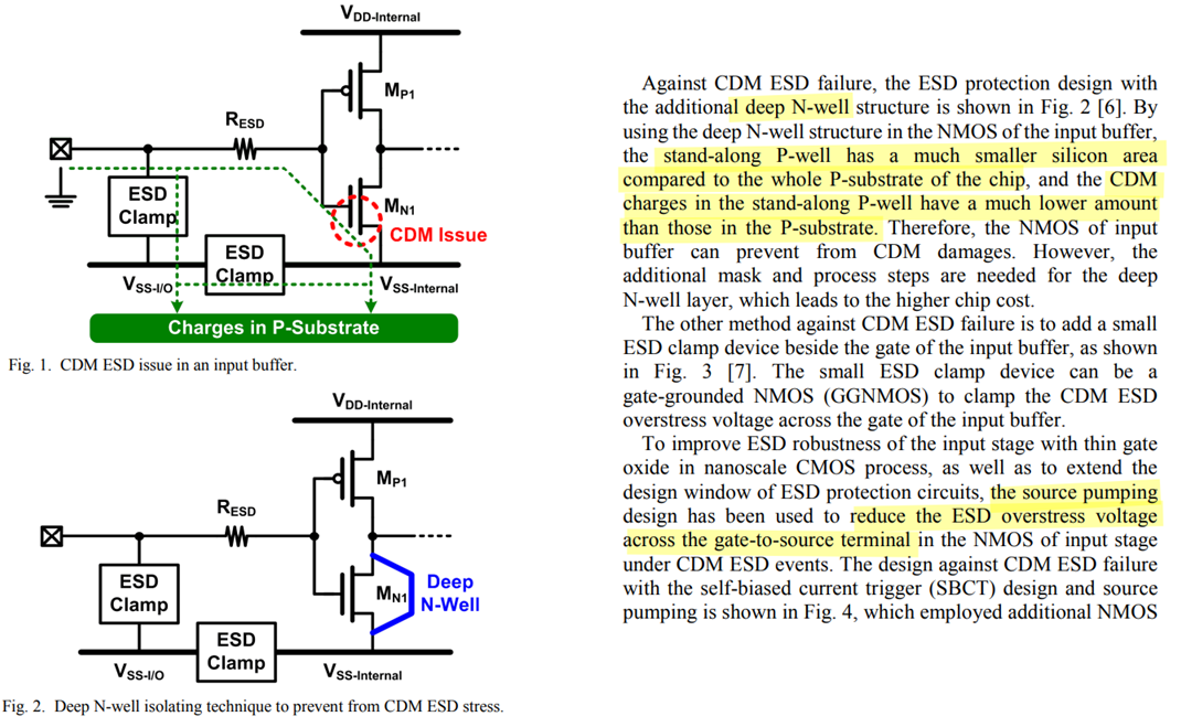
CDM Failure Mechanisms
reverse S/D junctions
capacitively coupled through the gate
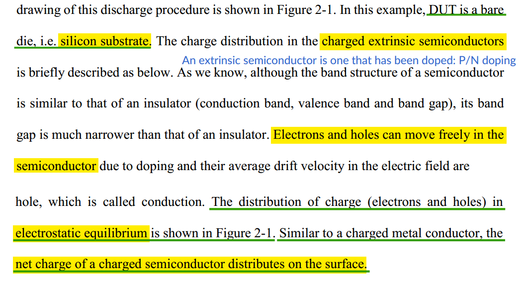
For a bare Si die, the charges induced by whatever procedures, are
stored inside the IC die randomly, unpredictably and anywhere, e.g., in
the substrate, along the metal
rails or locally to
transistors
?? suppose that charged package and substrate are same electric
potential
Misconception in CDM ESD
Protection
Two players will affect the internal CDM discharging routing:
the amount of electrostatic charge stored inside the IC
more importantly, their internal distribution within a chip
Wang, Han, Feilong Zhang, Cheng Li, Mengfu Di and Albert Z. H. Wang.
“Chip-Level CDM Circuit Modeling and Simulation for ESD Protection
Design in 28nm CMOS.” 2018 14th IEEE International Conference on
Solid-State and Integrated Circuit Technology (ICSICT) (2018) [pdf]
It is generally believed that the induced electrostatic charges are
stored on the package frame and/or on the
supply buses in a lumped way
induced electrostatic charges are randomly distributed throughout a
bare die of mixed-signal IC, anywhere and
everywhere
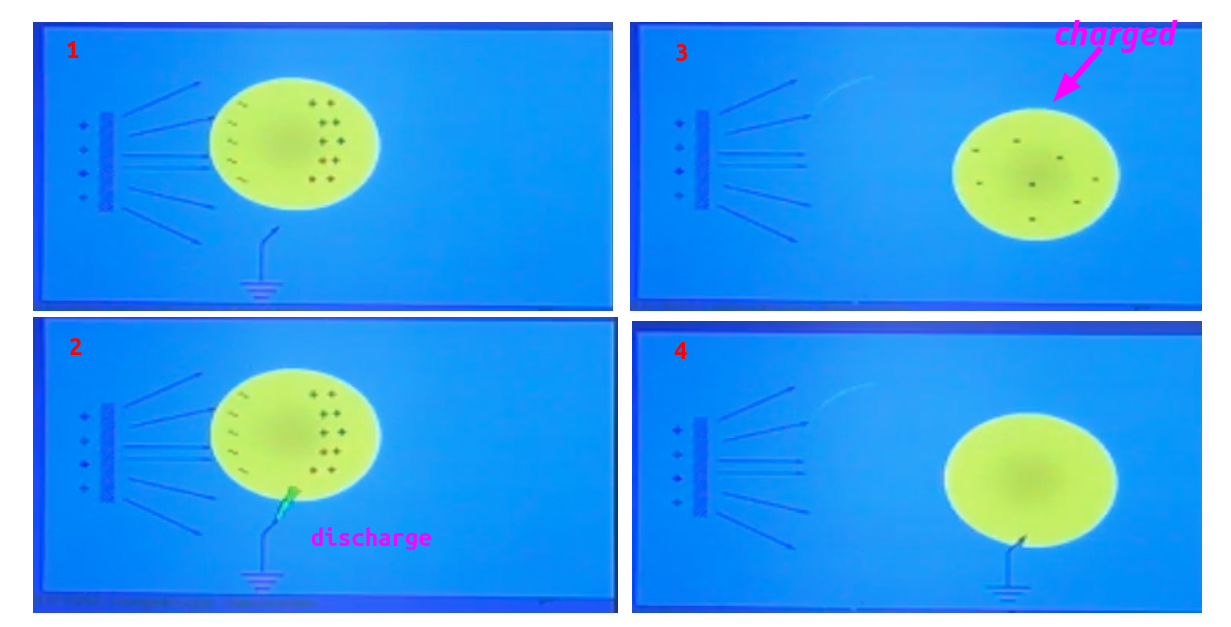
Confusion about the test procedure is
understandable because the actual process is opposite from what is
expected
field induction does not place any charge on the device
the "discharge" when the pogo pin first touches the DUT is when
the DUT is actually charged
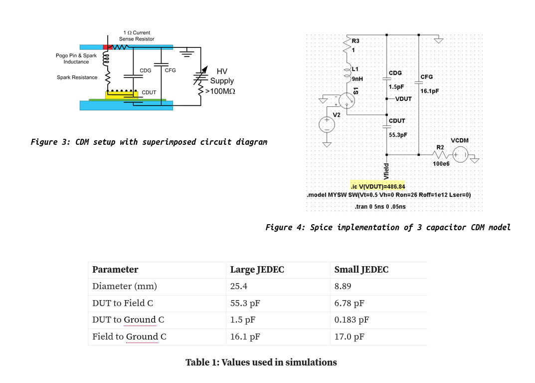
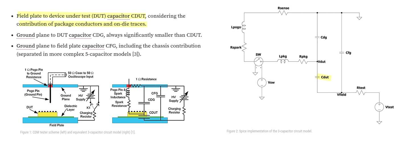
\(C_{DF}\) is the capacitance of the
DUT to the field plate
\(C_{DG}\) is the capacitance of the
DUT to the ground plane
\(C_{FG}\) is the capacitance of the
field plate to the ground plane
\(C_{DF}\gg C_{DG}\) — the
separation of the DUT from the field plate is always much less than the
separation of the DUT from the ground plane
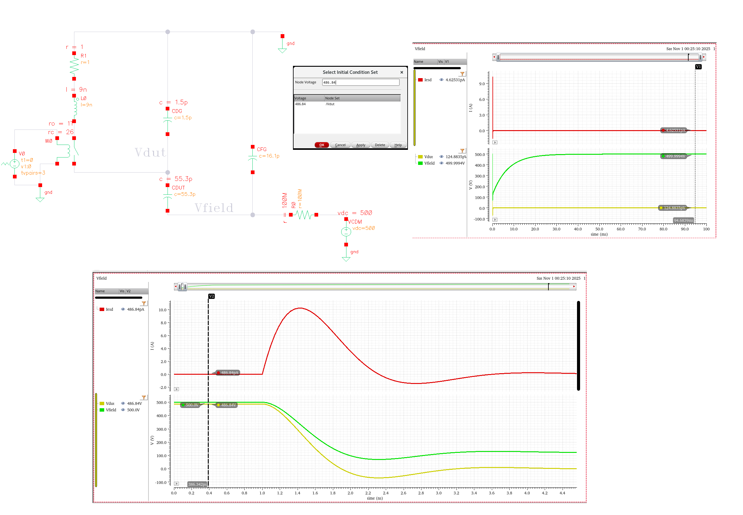
Assuming no initial charge on the DUT, with
the switch S open the DC voltage between the DUT and the Field Plate is
\[
V_{DF} = \frac{C_{DG}}{C_{DG} + C_{DF}}\cdot V_{HV} \approx 0
\]
DUT potential will therefore closely track
the power supply voltage
The potential of the DUT relative to the ground plane can
therefore be controlled without actually putting any net charge on
the DUT
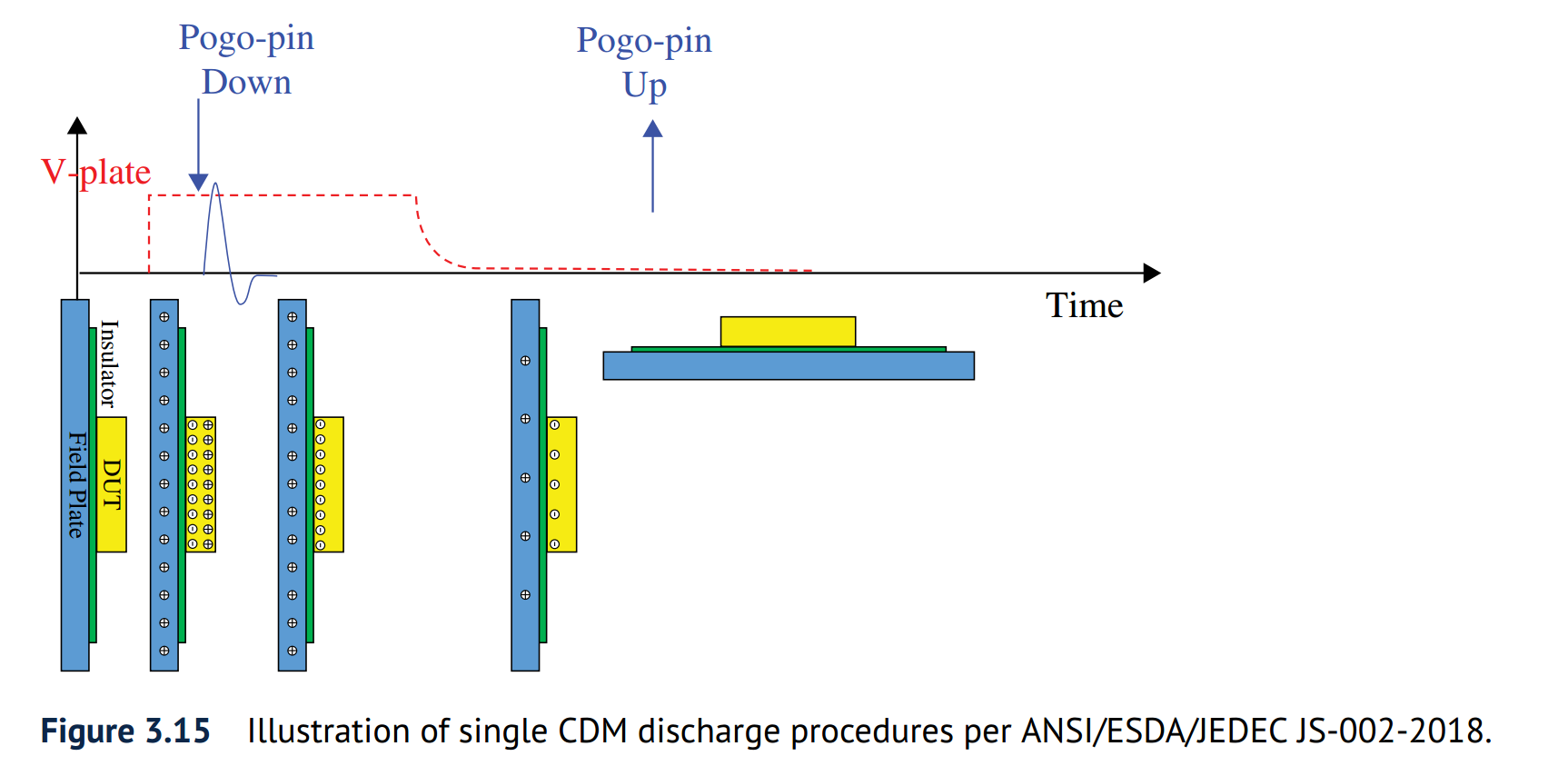
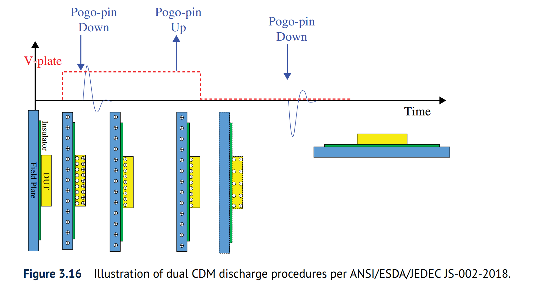
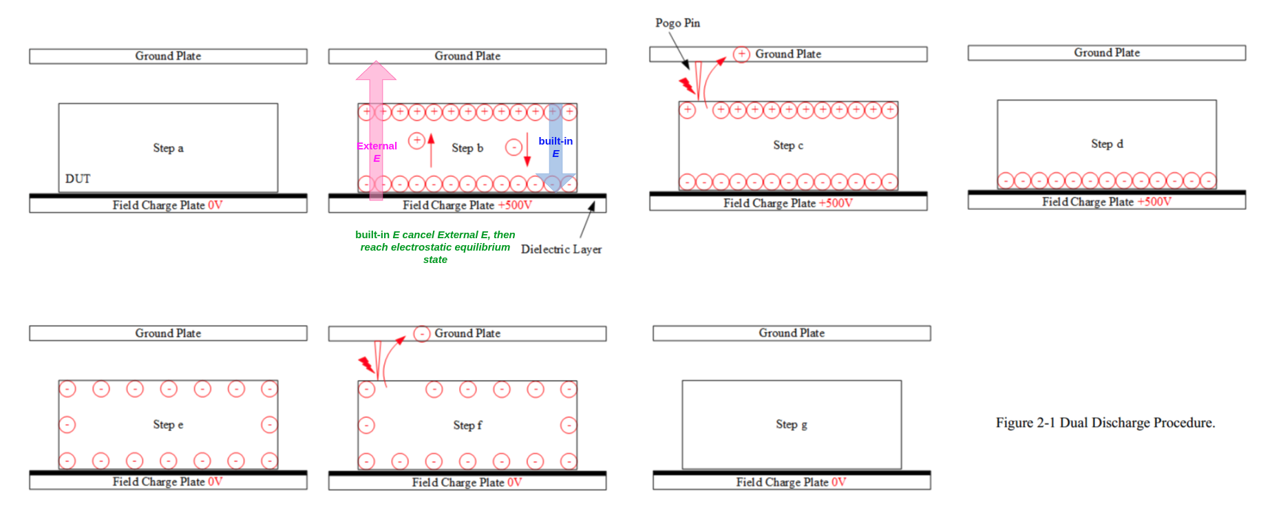
CDM Test Sequence
With the field plate at zero volts an uncharged
DUT is placed on the field plate in the dead bug position and the
ground plane is positioned with the pogo pin above the pin to be
tested
The field plate is raised to a high potential, for example +500
V. The high value resistor ensures that the field
plate changes potential relatively slowly. The slow change in potential
ensures that the DUT is not damaged before the CDM event.
The potential of the DUT will closely track the field plate, reaching
in excess of 450 V, although there will be no net charge on
the DUT
Capacitive coupling elevates the potential of the integrated circuit
to a voltage close to that of the field plate
After the voltage has stabilized the separation between the field
plate and the ground plane is reduced until an arc forms between the
pogo pin and the DUT pin and eventually the two pins touch.
This is equivalent to closing the switch S in Figure
3
Closing S in the circuit diagram produces a very
rapid grounding of the DUT and a redistribution of charge between the
three capacitors
At this point the DUT is charged and the
potential between the field plate and the ground plane has fallen as the
capacitor \(C_{FG}\) provides charge to
the DUT
During this redistribution of charge, which usually lasts under 2
ns, the high voltage power supply and the high value resistor can be
ignored because of their slow response time
After the initial redistribution of charge the field plate will
slowly return to the voltage on the high voltage power supply,
while the DUT remains at zero potential, but in a charged
state
With the pogo pin still touching the DUT pin the HV power supply
voltage is set to zero. The field plate will slowly return to zero volts
and the charge on the DUT will slowly bleed off through the
pogo pin.
single & dual discharge
method
single discharge procedure:
single positive orsingle negative
CDM ESD pulse is applied to DUT for individual CDM
discharge
the single discharge procedure involves only
one CDM discharge to stress the DUT device
dual discharge procedure:
single positive andsingle
negative CDM ESD pulses are applied to produce one pair of
alternating polarity CDM discharges to zap the DUT
The value of CFG is also based on a parallel plate capacitor model
with a peripheral capacitance term minus a capacitance
representing a shielding of the Field Plate to ground plane capacitance
due to the size of the device under test
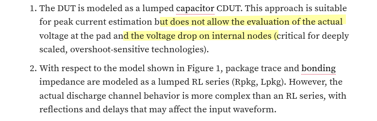
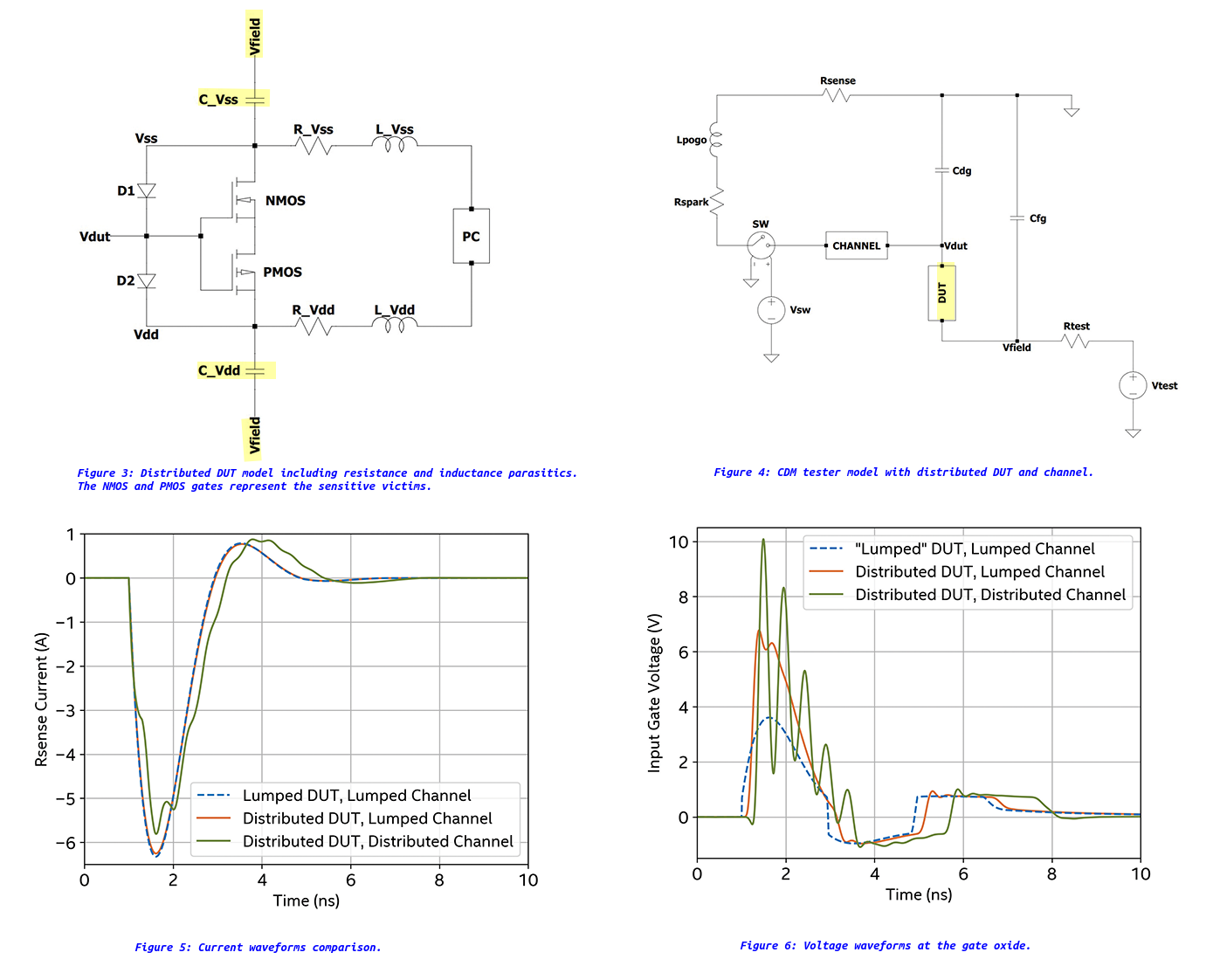
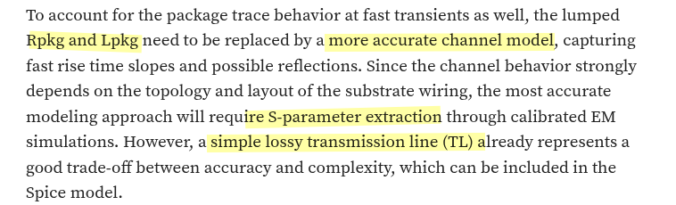
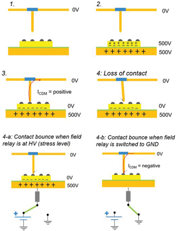
To assess the design solutions, a distributed DUT
model, as presented in Figure 3, can be plugged into the
CDM tester model, replacing the lumped DUT capacitor
The maximum voltage difference between Vdut and Vss (Vdd) should not
exceed the breakdown voltage of the gates.
On-die parasitics of Vss and Vdd nets
strongly influence the actual voltage waveform at the input gate
oxide. In particular, oscillations and spikes in the voltage
waveform are sensed by the gate oxide and can lead to damage
Lin, Chun-Yu and Ming-Dou Ker. “CDM ESD protection design with
initial-on concept in nanoscale CMOS process.” 2010 17th IEEE
International Symposium on the Physical and Failure Analysis of
Integrated Circuits (2010): 1-4. [https://sci-hub.jp/10.1109/IPFA.2010.5532223]
Jian-Hsing Lee et al., "The study of sensitive circuit and
layout for CDM improvement," 2009 16th IEEE International Symposium
on the Physical and Failure Analysis of Integrated Circuits,
Suzhou, China, 2009 [link]
Thanks to the device scaling the area is actually reasonable.
However, the leakage becomes the main bottleneck.
Y. -C. Huang and M. -D. Ker, "Investigation of CDM ESD Protection
Capability Among Power-Rail ESD Clamp Circuits in CMOS ICs With
Decoupling Capacitors," in IEEE Journal of the Electron Devices
Society, vol. 11, pp. 84-94, 2023 [pdf]
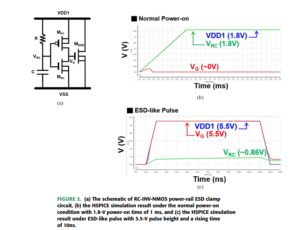
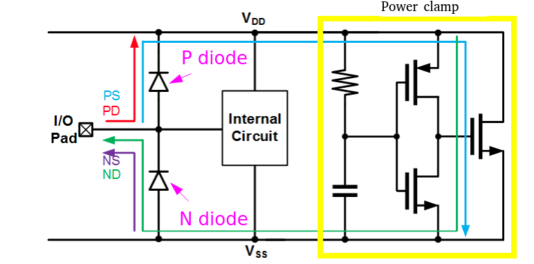
Dual Stacked Diodes
PS: I/O to GND positively
NS: I/O to GND negatively
PD: I/O to VDD positively
ND: I/O to VDD negatively
Dual diode should be used with power clamp for
PS and ND path
PMOS power clamp
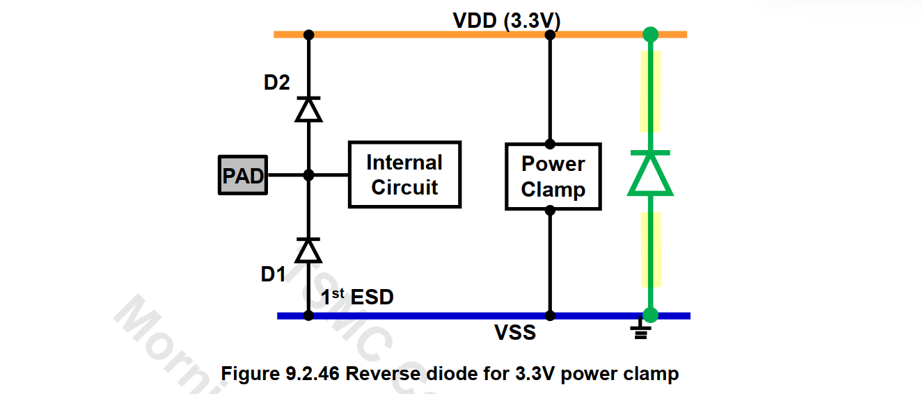
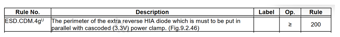
Reverse diode for
1.8V/3.3V power clamp
The resistance between HIA Diode and power/ground bump is constricted
in PERC check
Frank Feng. New Approach For Full Chip Electrical Reliability
Verification [pdf]
Calibre PERC Catalog Test-Cases & Common Examples Version 2.0
K. -H. Meng, M. Khazhinsky and J. C. Smith, "Effective ESD Design
Through PERC Programming," 2023 45th Annual EOS/ESD Symposium
(EOS/ESD), Riverside, CA, USA, 2023
Dina Medhat. Programmable Electrical Rule Checking (PERC) [pdf]
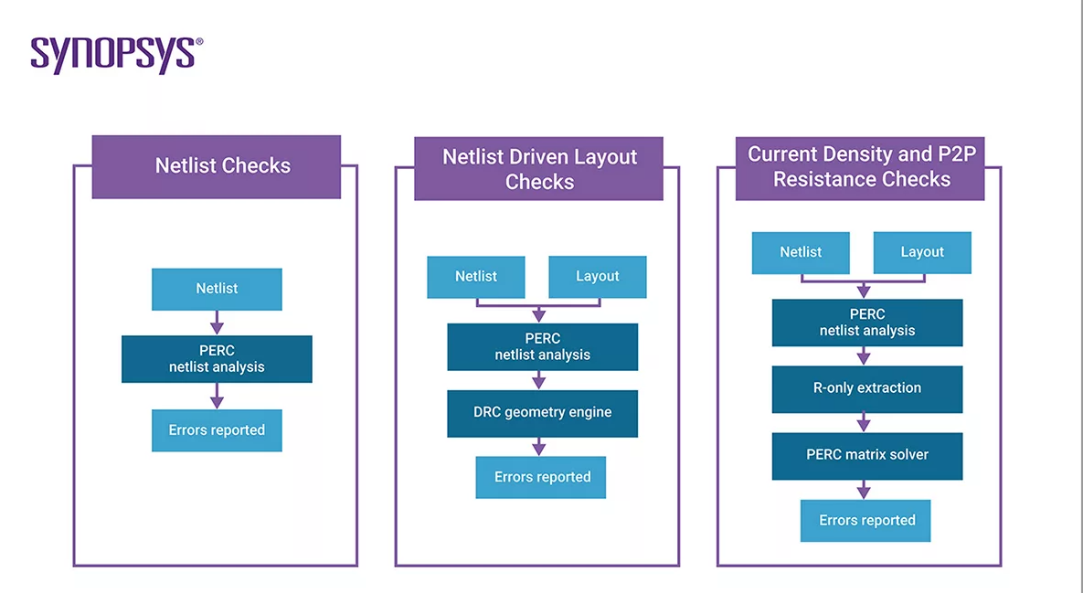
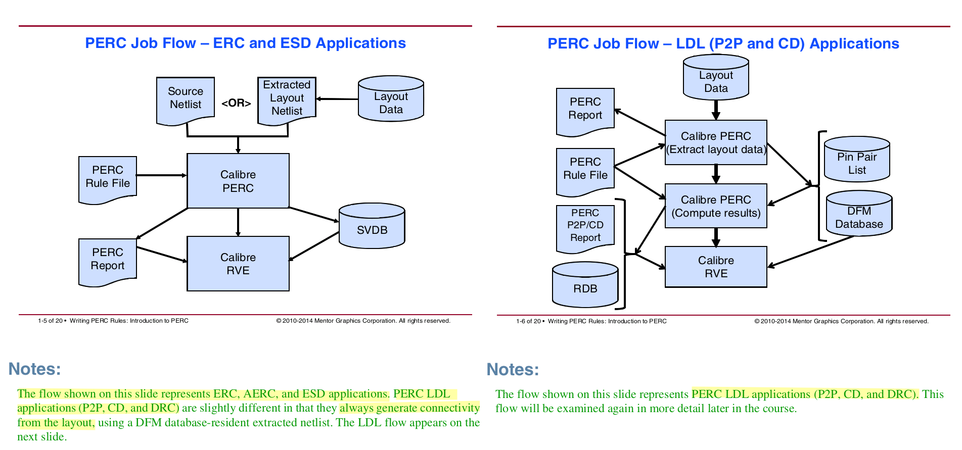
Programmable Electrical Rules Checking (PERC) is a method for
checking reliability issues of integrated circuit (IC) designs that
cannot be checked with design rule checking (DRC) or layout versus
schematic (LVS).
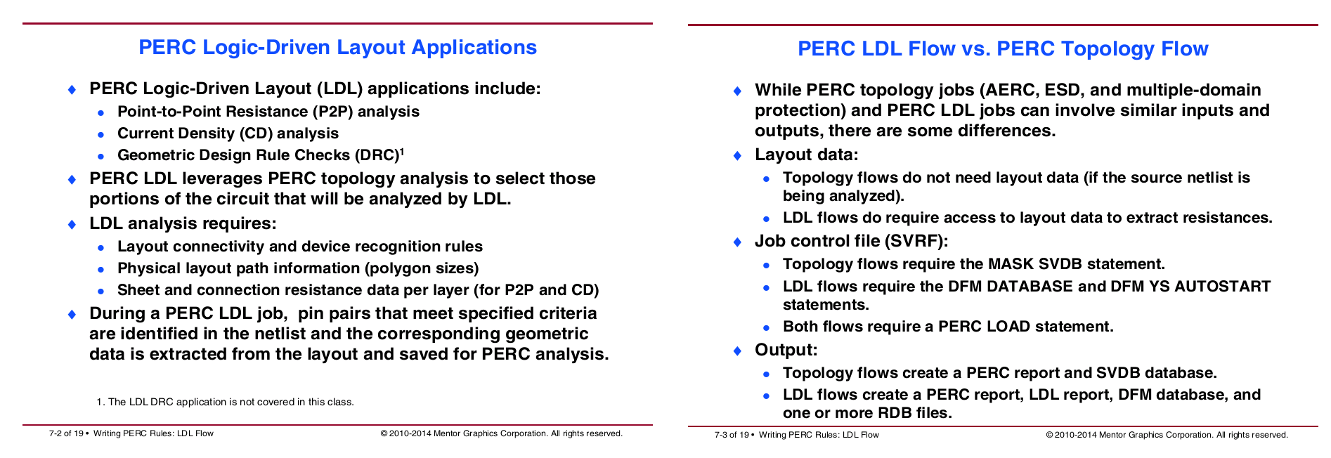
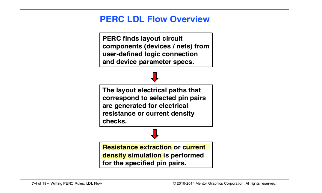
Topology (Circuit Connection and Device Size)
Check ESD protection scheme
LDL (Logic-Driven-Layout DRC)
Check Latch-up rules
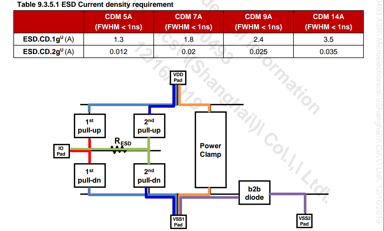
CD (Current Density)
Check primary, secondary ESD discharge path
P2P (Point-to-Point Resistance)
Check I/O to power-clamp path
pad_info
1 2 3 4 5 6 7 8 9 10 11
// Define PAD Voltage // VARIABLE "pad-text-name" pad-voltage VARIABLE "DVDD" 0.75 VARIABLE "DVSS" 0.75
// Define PAD Text // LAYOUT TEXT "pad-text-name" x-coor y-coor pin-text-layer
LAYOUT TEXT "DVDD" x0-coor y0-coor pin-text-layer LAYOUT TEXT "DVDD" x1-coor y1-coor pin-text-layer LAYOUT TEXT "DVSS" x2-coor y2-coor pin-text-layer
above <x0-coor y0-coor> and <x1-coor y1-coor> are shorted
together, in this way the two bump can share power clamp
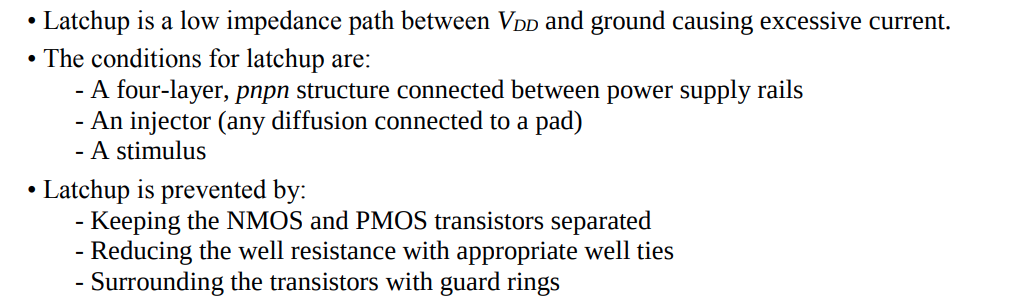
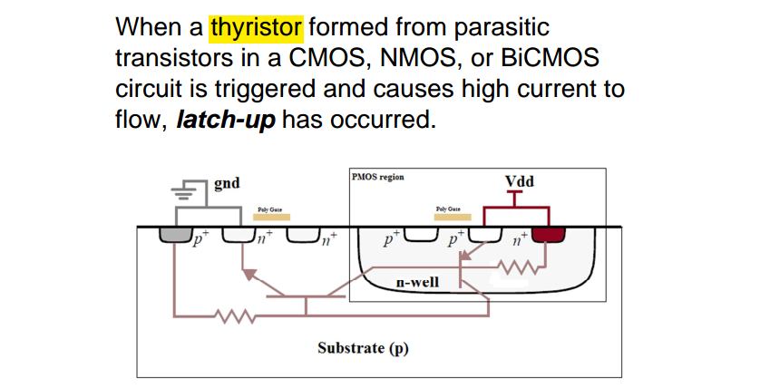
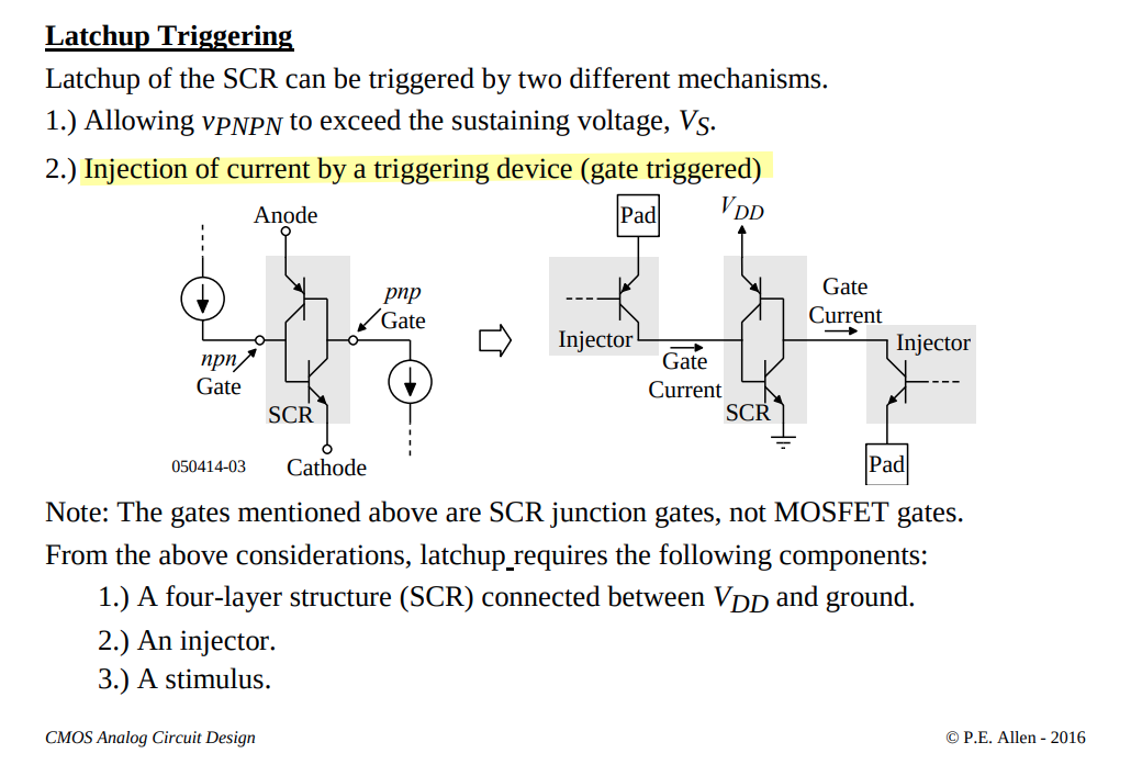
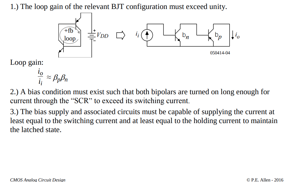
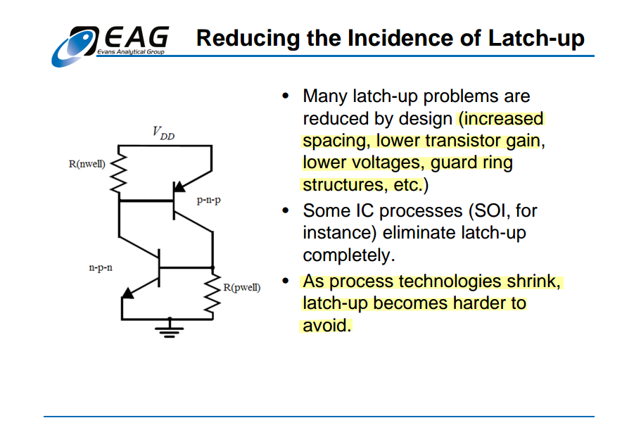
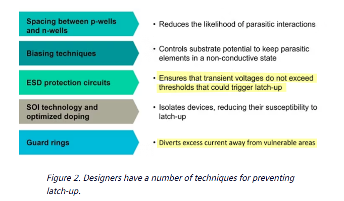
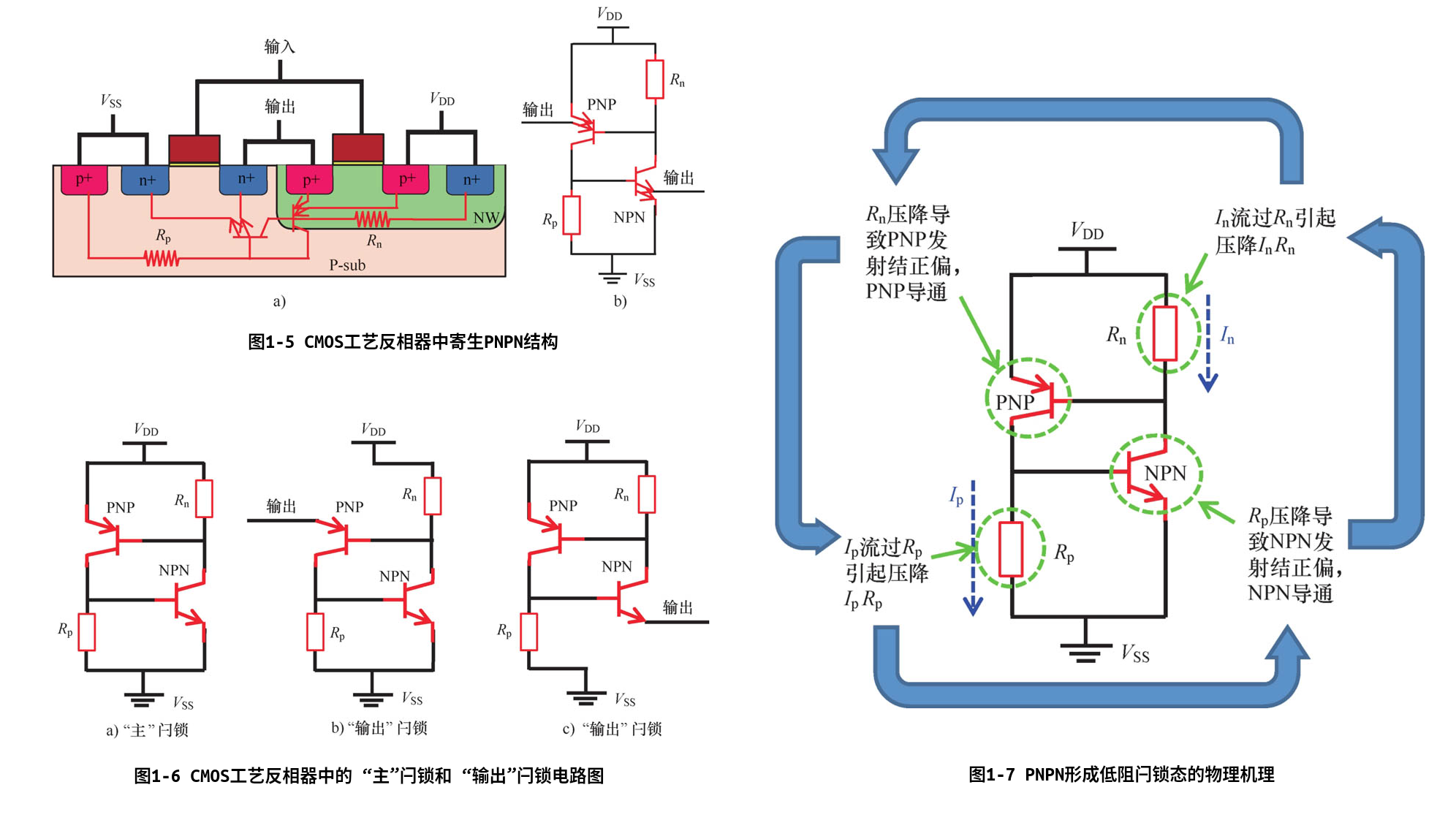
This can happen when a parasitic thyristor,
which is essentially a pair of interconnected
transistors, is triggered into a latched state, leading to
sustained current flow and potential device failure.
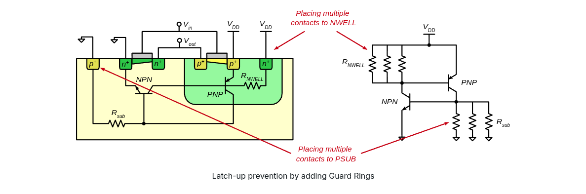
One important technique is the use of guard
rings, the heavily doped regions surrounding sensitive
components on the IC to divert excess current away from
vulnerable areas, thereby reducing the likelihood of latch-up
occurrence
These guard rings not only function as barriers against parasitic
thyristor (SCR) formation but also serve to isolate
different regions of the IC, minimizing unwanted electrical
interactions and maintaining pathway integrity
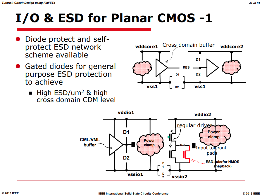
A diode can operate in both forward and reverse modes for ESD
protection.
\(R_{ON}\) for a forward-biased
diode is lower than that for a
reverse-biased diode
One major disadvantage of a forward diode-string for ESD protection
is that the leakage current (Ileak) may be enlarged due to the
Darlington effect in the diode-string
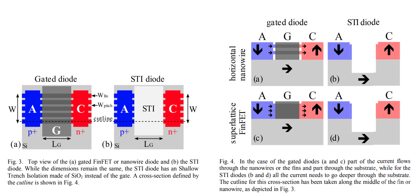
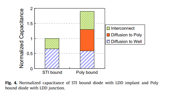
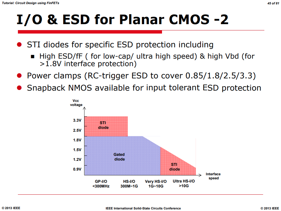
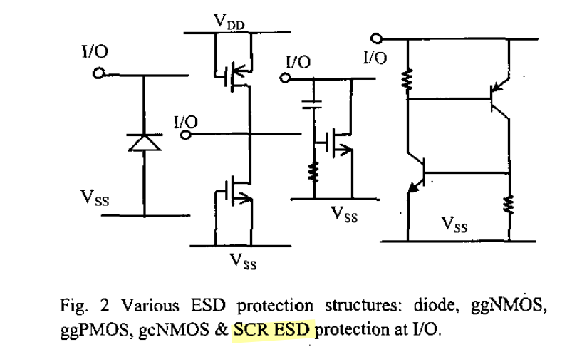
Gated diode & STI diode
"gated diode" aka. "poly bound" diode
STI bound diodes typically have lower
capacitance
M. Simicic, G. Hellings, S. -H. Chen, N. Horiguchi and D. Linten,
"ESD diodes with Si/SiGe superlattice I/O finFET architecture in a
vertically stacked horizontal nanowire technology," 2018 48th European
Solid-State Device Research Conference (ESSDERC), Dresden, Germany,
2018
US9653448B2. Electrostatic Discharge (ESD) Diode in FinFET
Technology
?? Rotated STI Diode
Loke, Alvin & Yang, (2018). Analog/mixed-signal design challenges
in 7-nm CMOS and beyond. 10.1109/CICC.2018.8357060.
Shih-Hung Chen. CICC 2019: Designing Diode Based ESD Protection in
Advanced State of the Art Technologies
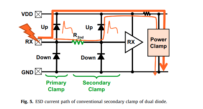
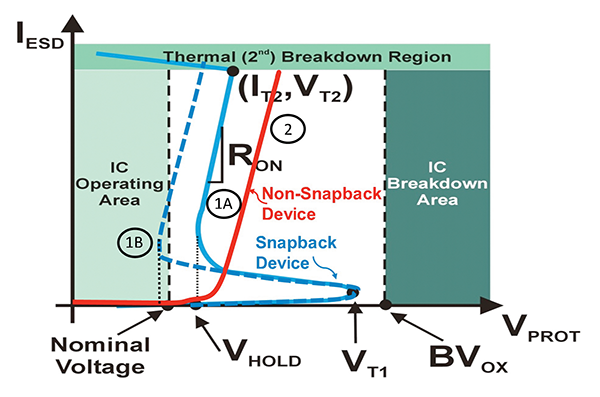
Two-Stage ESD Protection
two-stage primary–secondary ESD protection
a primary ESD protection structure (ESD1), a secondary ESD protection
unit (ESD2), and an isolation resistor (\(R\))
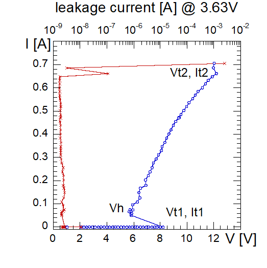
The desired specs for ESD2 is low \(V_\text{t1}\) and short
\(t_1\), while that for
ESD1 include low \(R_{ON}\), low \(V_\text{h}\) and high
\(I_\text{t2}\)
The primary ESD1 structure is typically optimized for high ESD
protection level, which however may feature a high ESD \(V_\text{t1}\), not suitable for low-voltage
(LV) ICs
The secondary ESD2 unit serves as a trigger-assisting device that
features a lower ESD \(V_\text{t1}\)
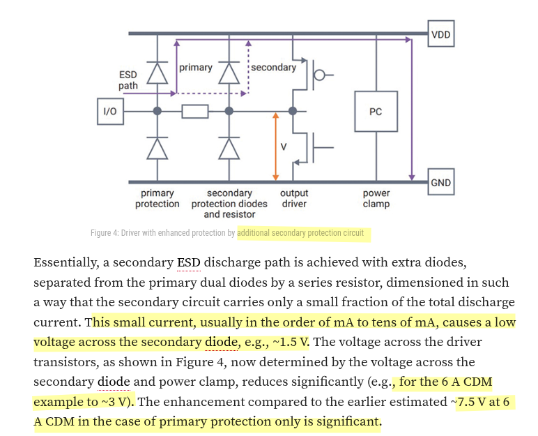
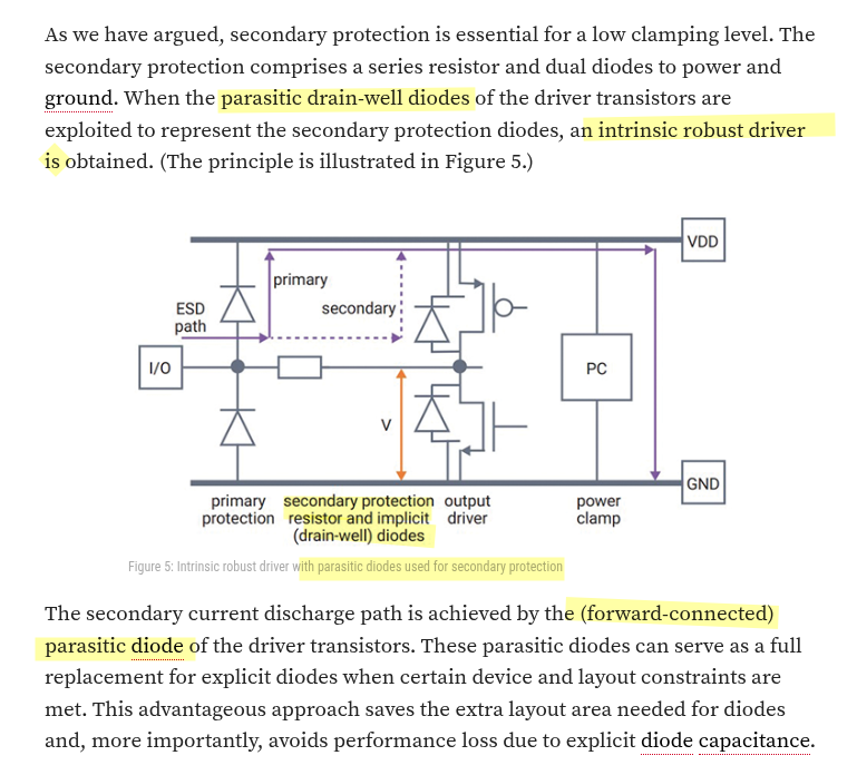
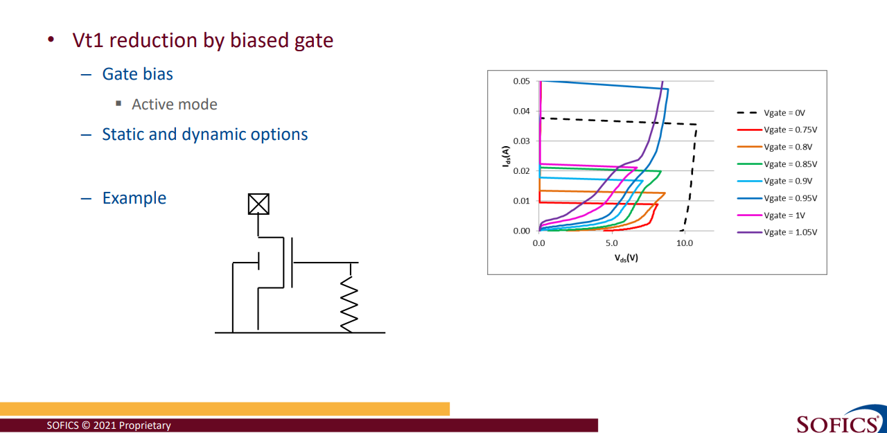
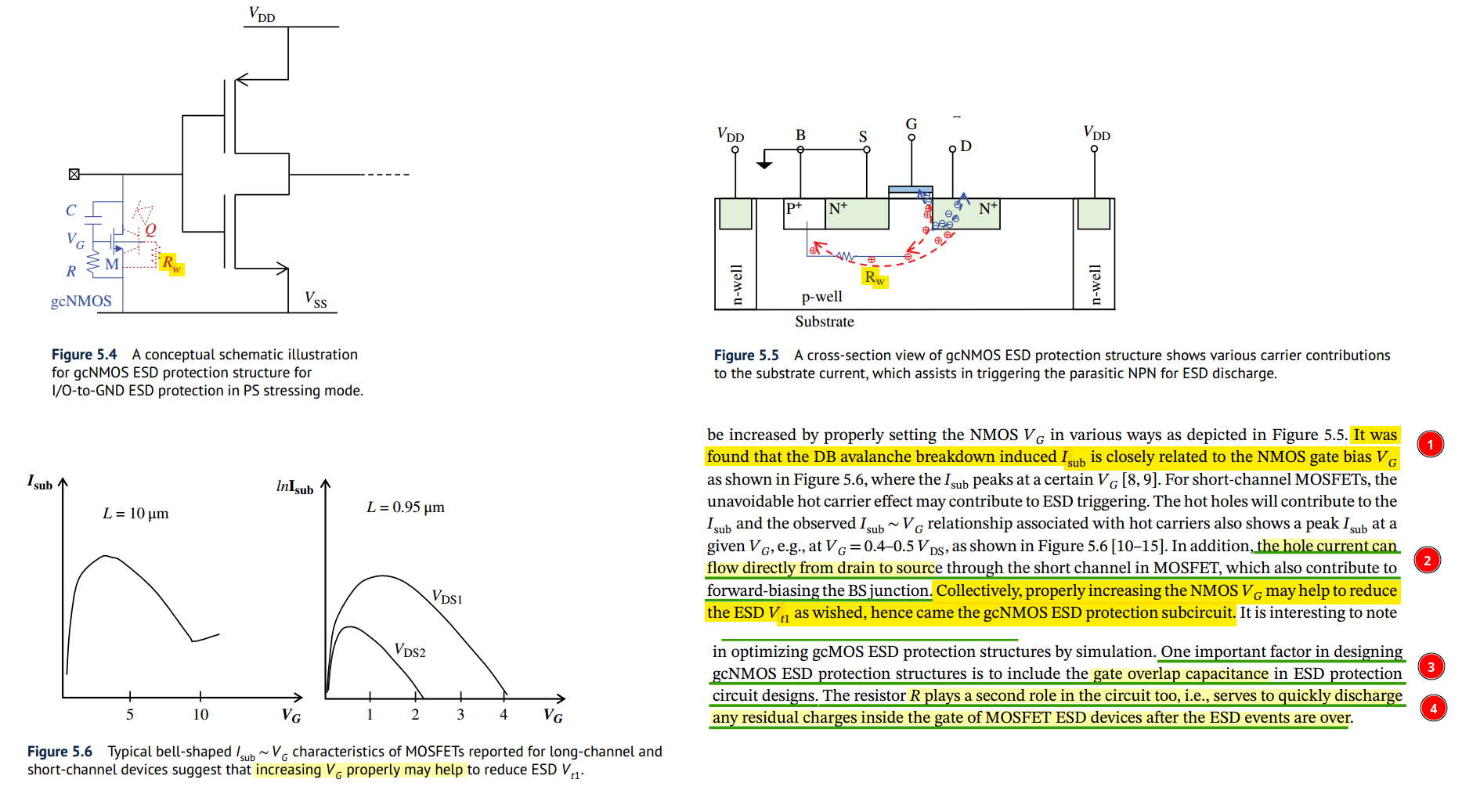
and fast ESD triggering, which is typically weak in handling large ESD
discharge currents
The isolation \(R\) has another
role, which is to prevent an ESD pulse from getting into IC core (i.e.,
stressing the input device) directly, hence avoid possible CMOS gate
breakdown
\(R\) involves a design trade-off
too: large enough for fast voltage build up, but not too large to avoid
adverse impact on signal propagation
The two-stage ESD protection method is re-gaining attention for
CDM ESD protection because it can handle large ESD
surges without overheating, while preventing CMOS gate
breakdown due to the isolation R (i.e., no direct zapping on the input
gate)
Adding a (small) clamp behind the isolation resistance can extend
the ESD design window, e.g. enabling dual diode protection for thin
oxide transistors.
ESD current through this clamp will build-up voltage across the
isolation resistance, while protecting the circuit.
The higher voltage at the IN pad will then trigger the primary
protection (red current path)
Adding a (small) clamp behind the isolation resistance can extend the
ESD design window, e.g. enabling dual diode protection
for thin oxide transistors
Extended ESD design window example. The failure voltage of a thin
gate oxide in advanced CMOS is about 4V. The primary ESD solution (red
IV curve) introduces too much voltage. Thanks to an isolation resistance
between primary and secondary local clamp device (green IV curve)
additional margin is created.
A thyristor (also known as a
Silicon Controlled Rectifier or
SCR) is a three-terminal semiconductor device used as
an electronic switch or rectifier
To turn the thyristor on, a positive voltage pulse is applied to the
gate (G) terminal. This voltage pulse needs to be of sufficient
magnitude to trigger the device. When the gate is triggered, it allows a
small current to flow into the base of the P-N-P transistor
within the thyristor structure
ESD tests simulate real world events (HBM, MM,
CDM)
TLP does not simulate any real-world event
ESD tests record failure level
(Qualification)
TLP tests record failure level and device behavior
(Characterization)
TLP is not a qualification test, but a characterization method, which
describes the resistance of a device for a given stimulus, aka.
Device Characterization
Unlike ESD waveforms, TLP does not mimic any real world event
TLP and Curve Tracing
Curve Tracing is DC; TLP is a short pulse
Shorter pulse - Reduced duty cycle, less heating, which means higher
voltage before failure
Controlled Impedance - Allows device behavior to be observed
Both measure resistance of device with increasing voltage
Device Characterization with
TLP
Turn-on time
Snapback voltage
Performance changes with rise time
VF-TLP and CDM differences
Question:
How well will VF-TLP results predict CDM testing performance?
Answer:
VF-TLP can be a guide to CDM failure levels, and provide a lot of
understanding of a circuit's operation during CDM stressing, but simple
correlations between VF-TLP failure current level and CDM withstand
voltage levels are difficult to establish.
I.V and Leakage Evolution
Plots
DC leakage current data combined with the I-V data provides
electrical indications of where damage begins, and how rapidly it can
evolve from soft to hard failures
Influence of the pulse rise time on ggNMOS. (left side) A fast ESD
pulse can couple the bulk of the NMOS to a higher potential for a short
period, reducing the trigger voltage. (right side) A clear Vt1 reduction
is visible, while the remaining part of the IV curve remains the
same.
Ming-Dou Ker, Chung-Yu Wu, Tao Cheng and Hun-Hsien Chang,
"Capacitor-couple ESD protection circuit for deep-submicron low-voltage
CMOS ASIC," in IEEE Transactions on Very Large Scale Integration
(VLSI) Systems, vol. 4, no. 3, pp. 307-321, Sept. 1996 [https://ir.lib.nycu.edu.tw/bitstream/11536/1053/1/A1996VE01800002.pdf]
Gate-coupled NMOS (gcNMOS) was proposed to
effectively reduce the \(V_\text{t1}\)
Guang Chen, Haigang Feng and A. Wang, "A systematic study of ESD
protection structures for RF ICs," IEEE Radio Frequency Integrated
Circuits (RFIC) Symposium, 2003, Philadelphia, PA, USA, 2003 [https://sci-hub.se/10.1109/RFIC.2003.1213959]
ANSI/ESDA/JEDEC JS-002-2022: ESDA/JEDEC Joint Standard For
Electrostatic Discharge Sensitivity Testing Charged Device Model (CDM)
Device Level
ESDA/JEDEC JTR002-01-22: For the User Guide of
ANSI/ESDA/JEDEC JS-002 Charged Device Model Testing of Integrated
Circuits
JESD22-C101E: Field-Induced Charged-Device Model Test Method
for Electrostatic Discharge-Withstand Thresholds of Microelectronic
Components
C. -Y. Lin and M. -D. Ker, "ESD Protection Design: Fundamentals and
Advanced Strategies," in IEEE Open Journal of the Solid-State Circuits
Society, vol. 6, pp. 61-76, 2026 [pdf]
M. Di, H. Wang, F. Zhang, C. Li, Z. Pan and A. Wang, "Does CDM ESD
Protection Really Work?," 2019 IEEE Workshop on Microelectronics and
Electron Devices (WMED), Boise, ID, USA, 2019 [https://sci-hub.se/10.1109/WMED.2019.8714145]
M. Di, C. Li, Z. Pan and A. Wang, "Pad-Based CDM ESD Protection
Methods Are Faulty," in IEEE Journal of the Electron Devices
Society, vol. 8, pp. 1297-1304, 2020 [pdf]
S. Kim et al., "Technology Scaling of ESD Devices in State of the Art
FinFET Technologies," 2020 IEEE Custom Integrated Circuits Conference
(CICC), 2020, pp. 1-6, doi: 10.1109/CICC48029.2020.9075899.
Yuanzhong Zhou, D. Connerney, R. Carroll and T. Luk, "Modeling MOS
snapback for circuit-level ESD simulation using BSIM3 and VBIC models,"
Sixth international symposium on quality electronic design (isqed'05),
2005, pp. 476-481, doi: 10.1109/ISQED.2005.81.
M. -D. Ker and Z. -H. Jiang, "Overview on Latch-Up Prevention in CMOS
Integrated Circuits by Circuit Solutions," in IEEE Journal of the
Electron Devices Society, vol. 11, pp. 141-152, 2023 [https://ieeexplore.ieee.org/stamp/stamp.jsp?arnumber=9998049]
Y. Li, M. Miao and R. Gauthier, "ESD Protection Design Overview in
Advanced SOI and Bulk FinFET Technologies," 2020 IEEE Custom
Integrated Circuits Conference (CICC), Boston, MA, USA, 2020
S. Kim et al., "Technology Scaling of ESD Devices in State
of the Art FinFET Technologies," 2020 IEEE Custom Integrated
Circuits Conference (CICC), Boston, MA, USA, 2020
Jitter separation lets you learn if the components
of jitter are random or deterministic. That is, if they are caused by
crosstalk, channel loss, or some other phenomenon. The identification of
jitter and noise sources is critical when debugging failure sources in
the transmission of high-speed serial signals
Tail Fit Method
Spectral method
RJ Extraction Methods
Rationale
Spectral
Speed/Consistency to Past Measurements; Accuracy in low
Crosstalk or Aperiodic Bounded Uncorrelated Jitter (ABUJ)
conditions
Tail Fit
General Purpose; Accuracy in high Crosstalk or ABUJ
conditions
power spectral density (PSD) represents jitter spectrum and peaks in
the spectrum can be interpreted as PJ or DDJ, while the average noise
floor is the power of RJ
1 2 3 4 5 6 7 8 9 10 11 12 13 14 15 16 17
S1 = sum(win); S2 = sum(win.^2); N = length(win); spec_nospur2 = (spec_nospur*S1).^2/N/S2; % To obtain linear spectrum for rj rj_utj = sqrt(sum(spec_nospur2))*1e12;
spec = 1*ones(length(spec_nospur), 1)*1e-21; spec(index) = specx(index); % insert fft nyquist frequency component between positive frequency and % negative frequency component % DC;posFreq;nyqFreq;negFreq spec_ifft = [spec;specnyq;conj(spec(end:-1:2))]'; sfactor = sum(win)/sqrt(2); spec_ifft = spec_ifft*sfactor; sig_rec = real(ifft(spec_ifft)); sig_rec = sig_rec(:); sig_rec_utj = sig_rec./win(1:end);
Tail Fit Method
Tail fitting algorithm based on the Gaussian tail
model by using probability distribution of collected jitter
value
1 2 3 4 5 6 7 8 9 10 11 12 13
bin_sig = bin_sig*1e12;

x = qfuncinv(cdf_sig);

% coef(1)*bin_sig + coef(2) = x
% which x is norm(0, 1)
% bin_sig = (x - coef(2))/coef(1)
% Then bin is norm(-coef(2)/coef(1), 1/coef(1))
coef = polyfit(bin_sig, x, 1);
sigma = 1/coef(1);
mu = -coef(2)*sigma;

fprintf('sigma=%.3fps, mu=%.3fps\n', sigma, mu);
Least Squares (LS) method
It is known that TIE jitter is a linear equation, shown in below
formula \[
x[n] = d_n \times \left[ \Delta t_{pj}[n]+\Delta t_{DCD}[n] +\Delta
t_{ISI}[n]+\Delta t_{RJ}[n]\right]
\] LS can be used to estimate the PJ, DCD, RJ , and ISI
parameters \([a,b,J_{DCD},J_0,
J_1...J_{(2^k-1)}]\)
Jitter modeling
Periodic Jitter (PJ)
PJ is a repeating jitter \[
\Delta t_{PJ}[n]=A\sin(2\pi f_0\cdot nT_s + \theta)=a \sin(2\pi f_0
\cdot nT_s)+b\cos(2\pi f_0 \cdot nT_s)
\] where \(f_0\) represents the
fundamental frequency of PJ; \(A\) is
the amplitude of PJ; \(T_s\) is the
data stream period, and \(\theta\) is
the initial phase of PJ
In the spectrum, the frequency of maximum amount of the jitter is PJ
frequency \(f_0\).
Duty Cycle Distortion (DCD)
DCD is viewed as a series of adjacent positive and negative
impulses\[
\Delta t_{DCD}[n] = J_{DCD}\times (-1)^n =
[-J_{DCD},J_{DCD},-J_{DCD},J_{DCD},...]
\] Where \(J_{DCD}\) is the DCD
amplitude.
Random Jitter (RJ)
RJ is created by unbounded jitter sources, such as Gaussian white
noise. The statistical PDF for RJ is enerally treated as a Gaussian
distribution \[
f_{RJ}(\Delta t) = \frac{1}{\sqrt{2\pi\sigma}}\exp(-\frac{(\Delta
t)^2}{2\sigma^2})
\]
DJ/RJ
K. Bidaj, J. -B. Begueret, N. Houdali, J. Deroo and S. Rieubon,
"Time-domain PLL modeling and RJ/DJ jitter decomposition," 2016 IEEE
International Symposium on Circuits and Systems (ISCAS), Montreal, QC,
Canada, 2016 [https://sci-hub.se/10.1109/ISCAS.2016.7527201]
Periodic Jitter Generator
& Insertion
Analysis and Estimation of Jitter Sub-Components: Classification
and Segregation of Jitter Components
Reference
Li, Mike Peng. Jitter, Noise, and Signal Integrity at High-
Speed. Prentice Hall, 2008.
—,DesignCon2007, Simultaneous Jitter Analysis in Time, Frequency,
and Statistical Domains and Their Interrelationships [pdf]
—,DesignCon2023, Accuracy and Challenges of PAM4 jitter and noise
measurements for >100Gbps Serial Links [pdf]
—, "A new method for jitter decomposition through its distribution
tail fitting," International Test Conference 1999. Proceedings (IEEE
Cat. No.99CH37034), 1999, pp. 788-794, [https://sci-hub.jp/10.1109/TEST.1999.805809]
Y. Duan and D. Chen, "Accurate jitter decomposition in high-speed
links," 2017 IEEE 35th VLSI Test Symposium (VTS), 2017, pp. 1-6, doi:
10.1109/VTS.2017.7928918.
Y. Duan and D. Chen, "Fast and Accurate Decomposition of
Deterministic Jitter Components in High-Speed Links," in IEEE
Transactions on Electromagnetic Compatibility, vol. 61, no. 1, pp.
217-225, Feb. 2019, doi: 10.1109/TEMC.2018.2797122.
"Jitter Analysis: The Dual-Dirac Model, RJ/DJ, and Q-Scale",
Whitepaper: Keysight Technologies, U.S.A., Dec. 2017
Sharma, Vijender Kumar and Sujay Deb. "Analysis and Estimation of
Jitter Sub-Components." (2014).
Qingqi Dou and J. A. Abraham, "Jitter decomposition in ring
oscillators," Asia and South Pacific Conference on Design Automation,
2006
E. Balestrieri, L. De Vito, F. Lamonaca, F. Picariello, S. Rapuano
and I. Tudosa, "The jitter measurement ways: The jitter decomposition,"
in IEEE Instrumentation & Measurement Magazine, vol. 23, no. 7, pp.
3-12, Oct. 2020, doi: 10.1109/MIM.2020.9234759.
McClure, Mark Scott. "Digital jitter measurement and separation." PhD
diss., 2005.
Ren, Nan, Zaiming Fu, Shengcu Lei, Hanglin Liu, and Shulin Tian.
"Jitter generation model based on timing modulation and cross point
calibration for jitter decomposition." Metrology and Measurement Systems
28, no. 1 (2021).
K. Bidaj, J. -B. Begueret and J. Deroo, "RJ/DJ jitter decomposition
technique for high speed links," 2016 IEEE International Conference
on Electronics, Circuits and Systems (ICECS) [https://sci-hub.se/10.1109/ICECS.2016.7841269]
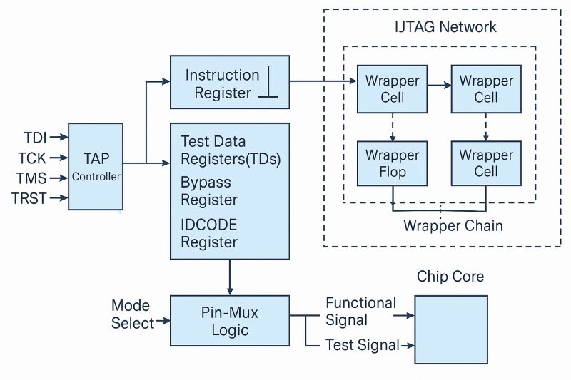
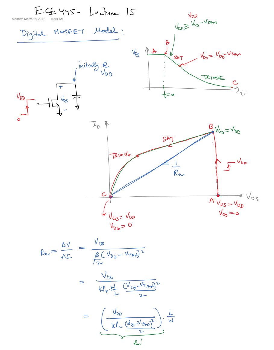
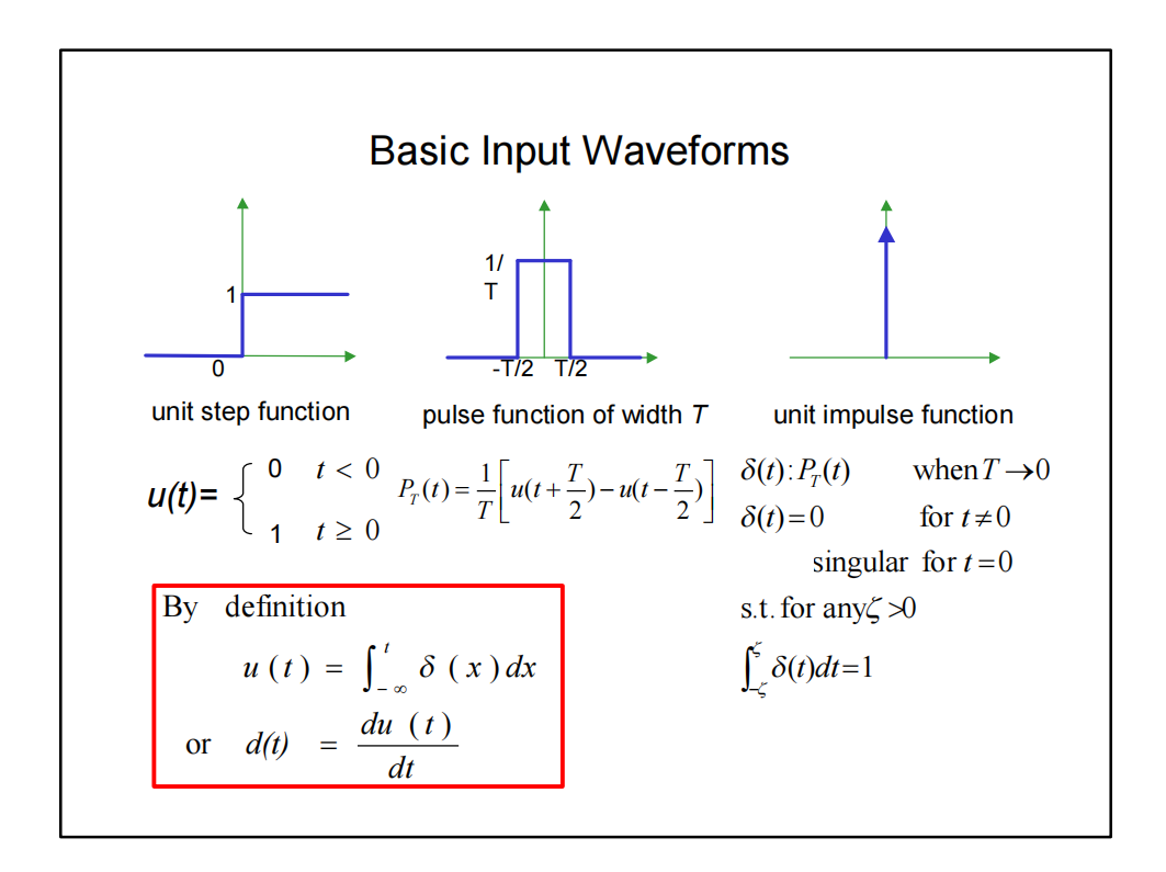
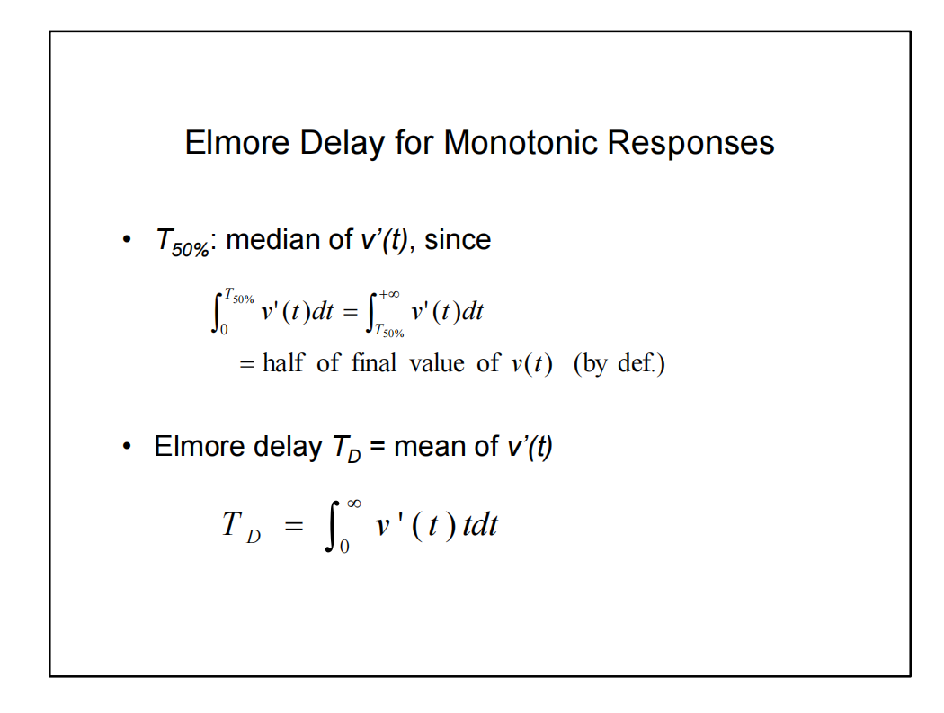
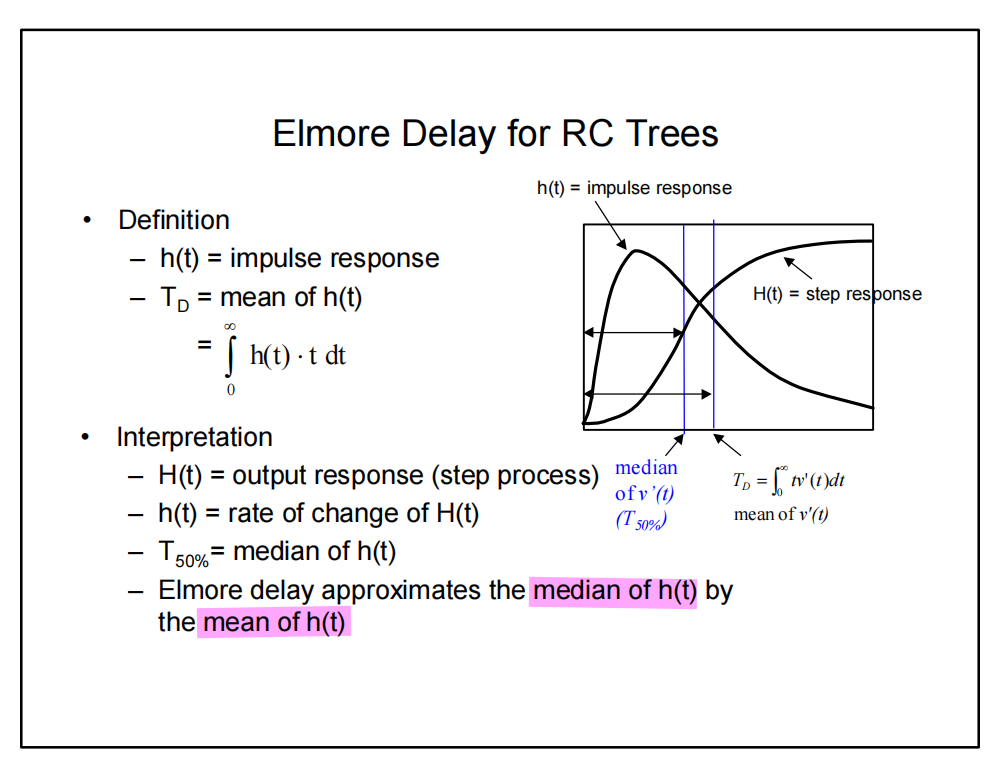
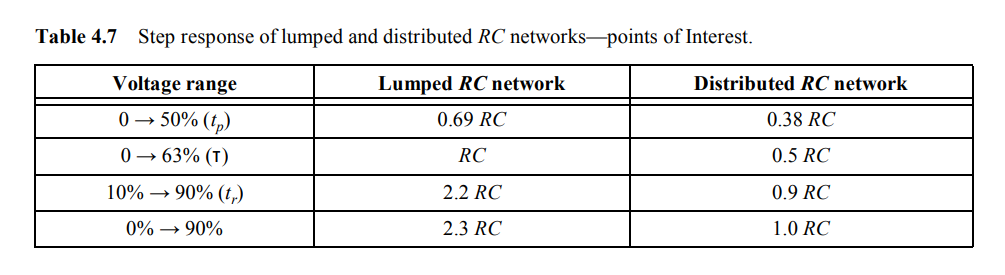
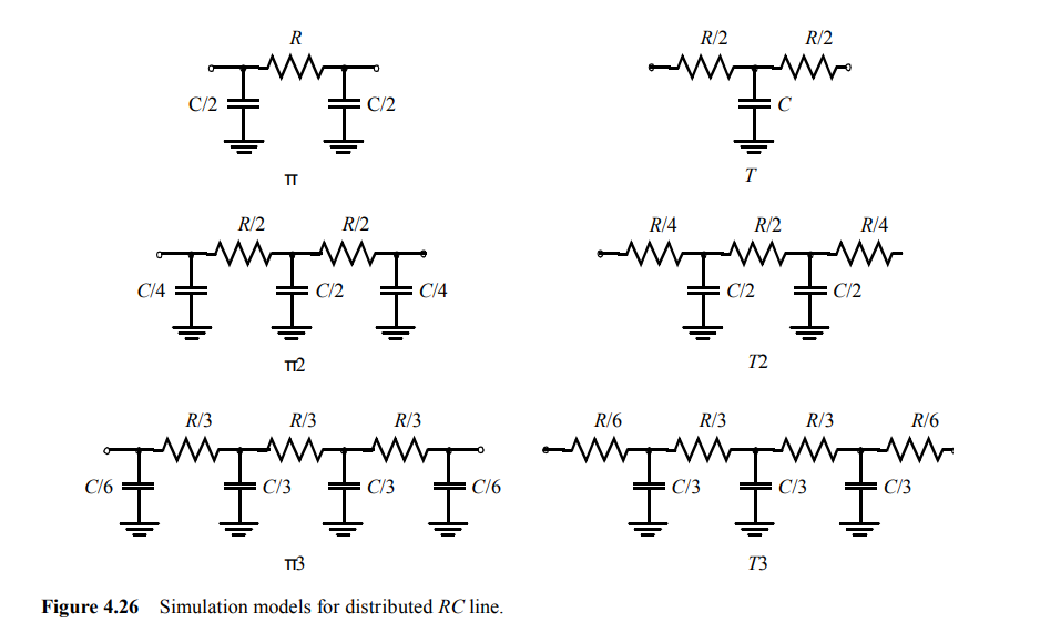
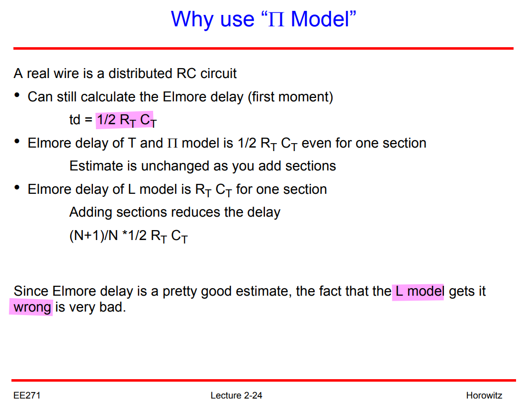
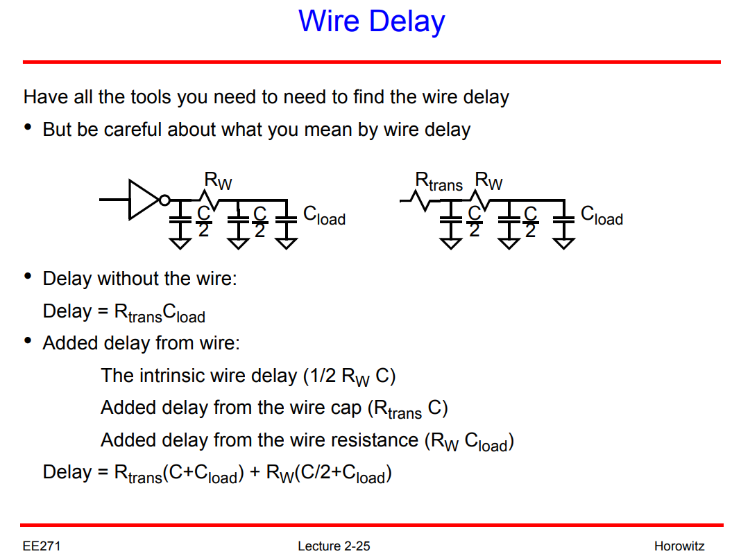
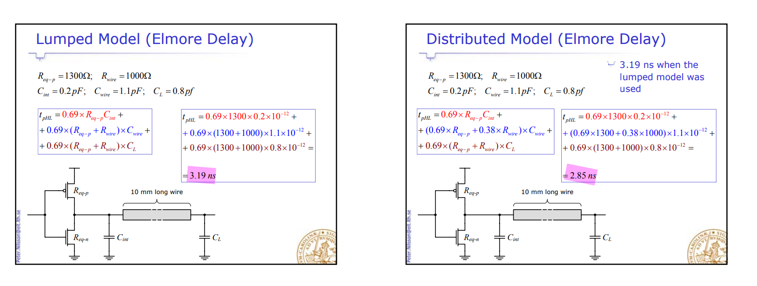
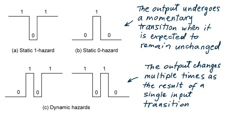

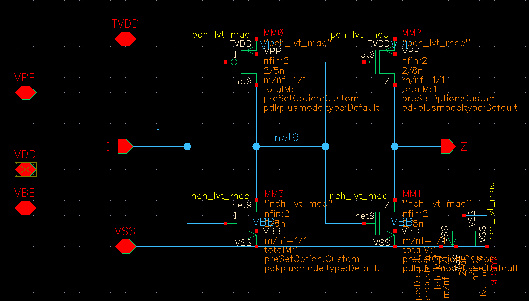
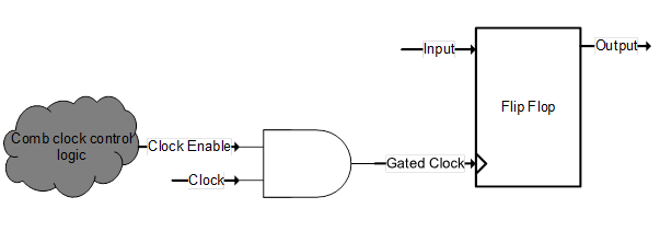
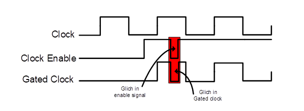
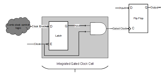
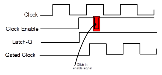
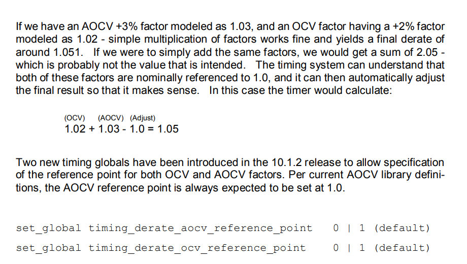
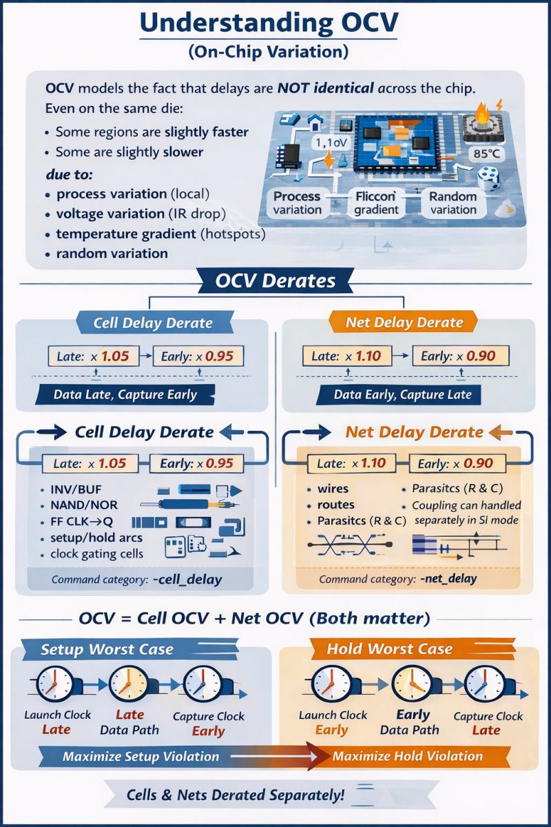
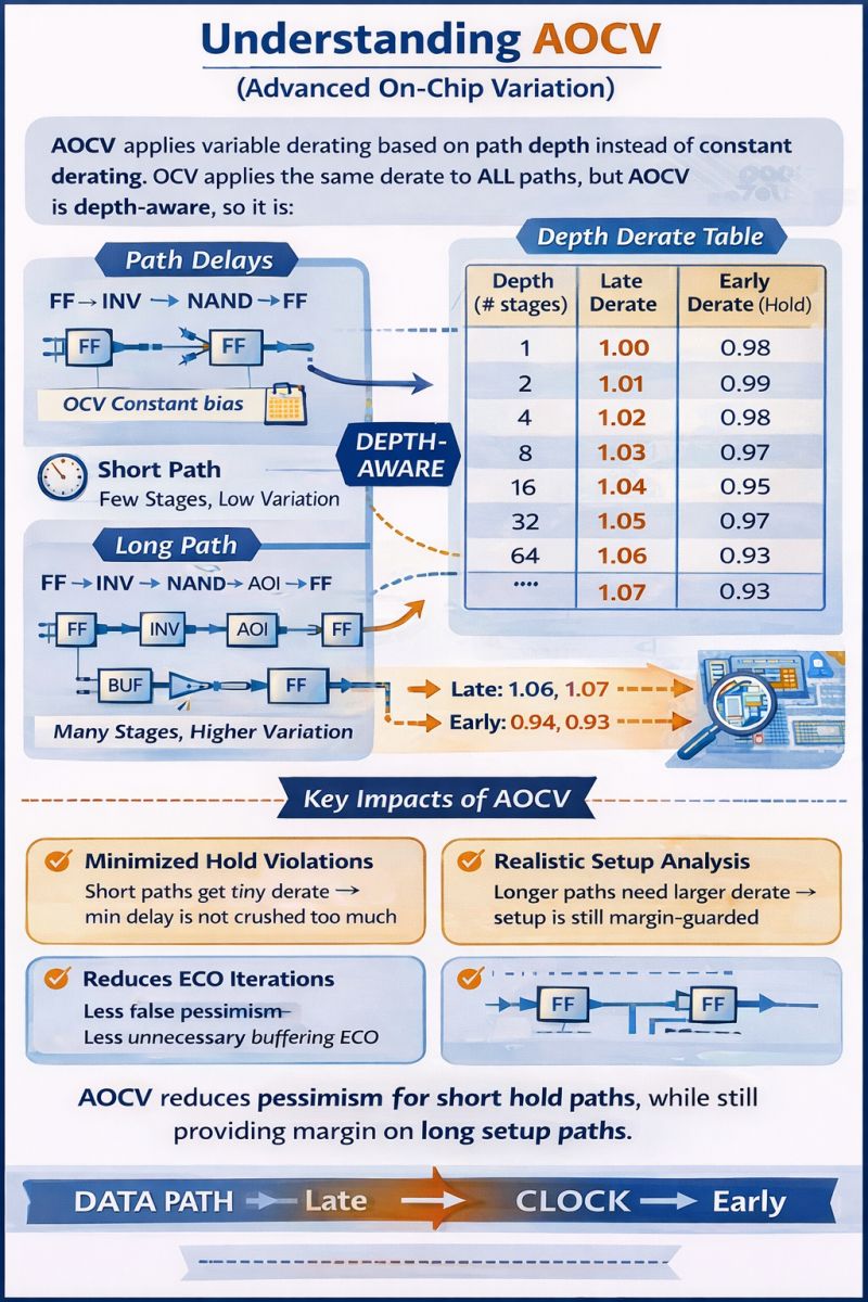
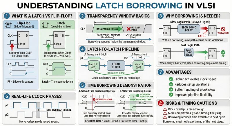

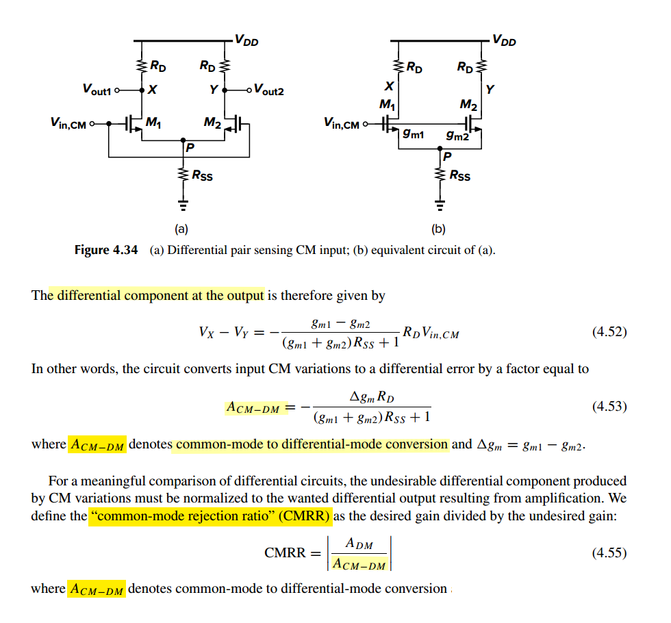
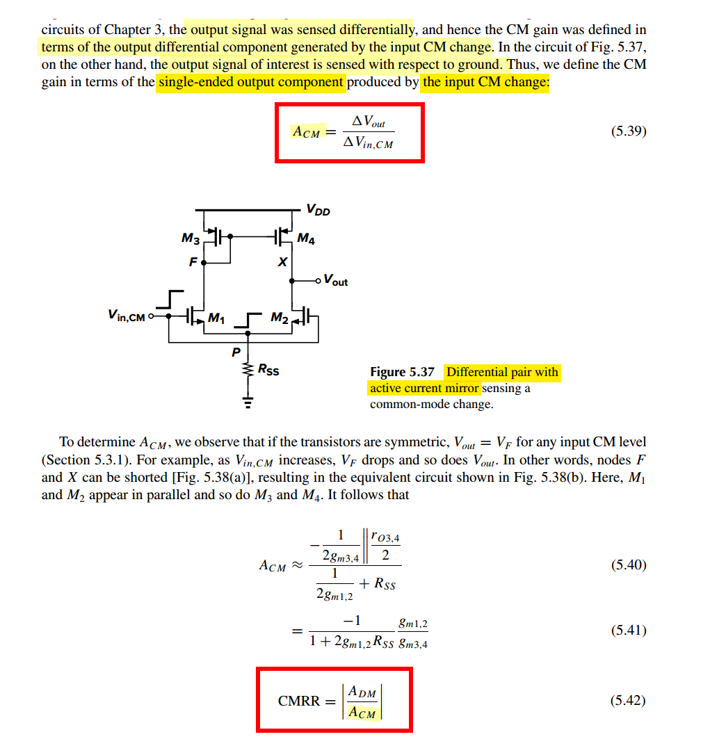
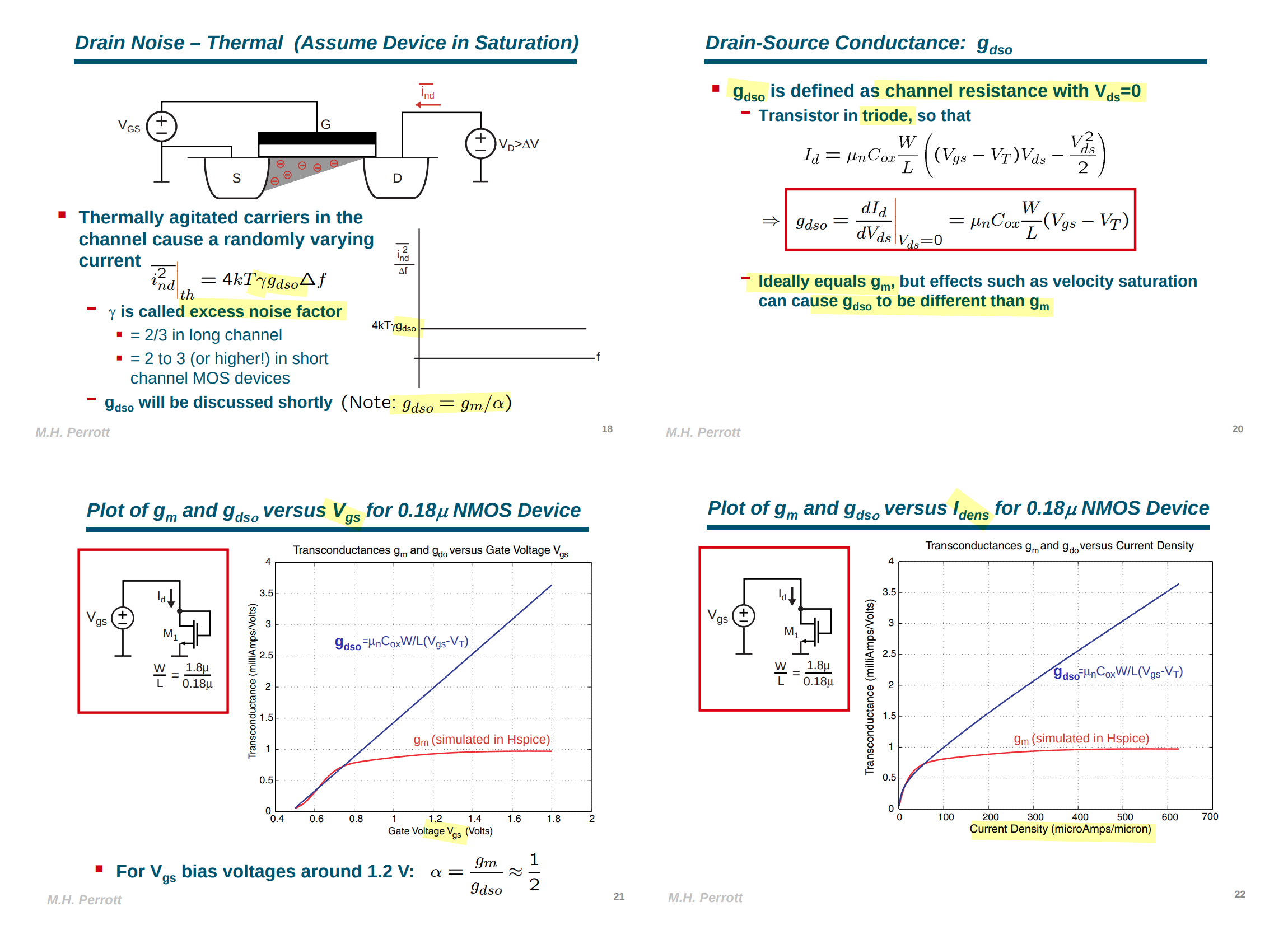
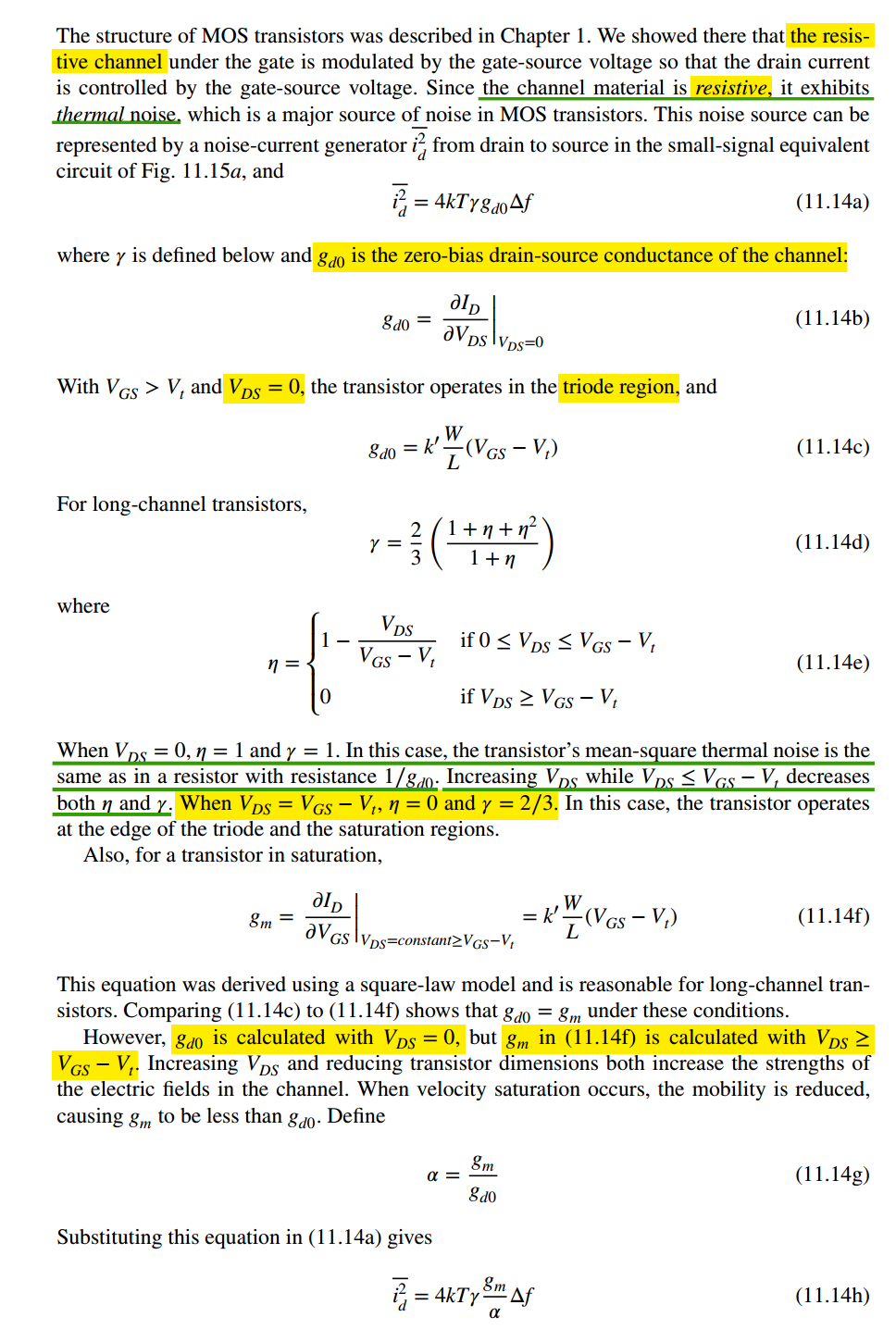
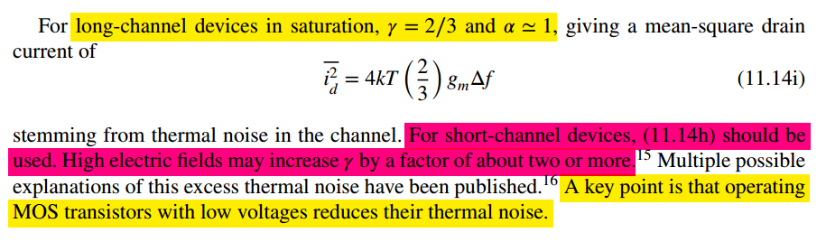

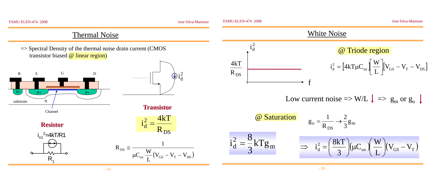
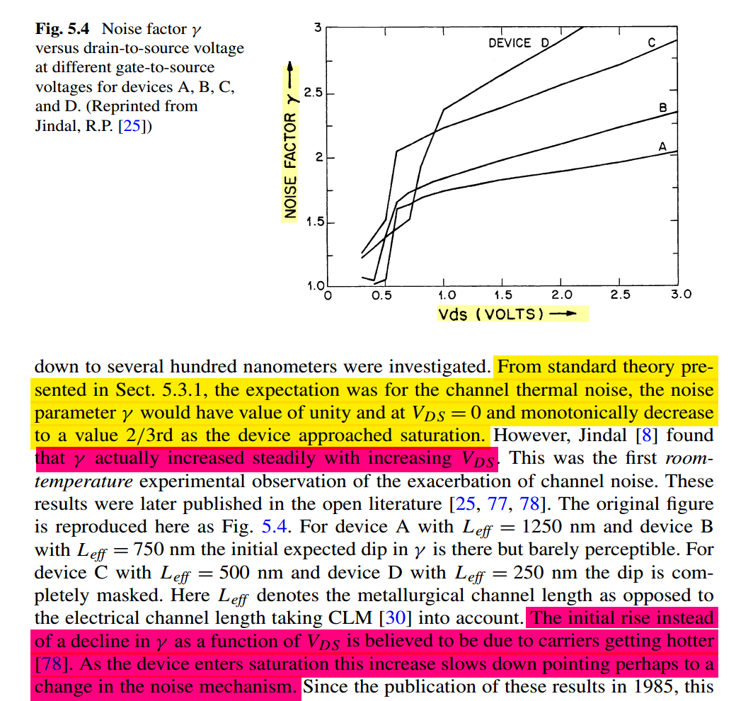
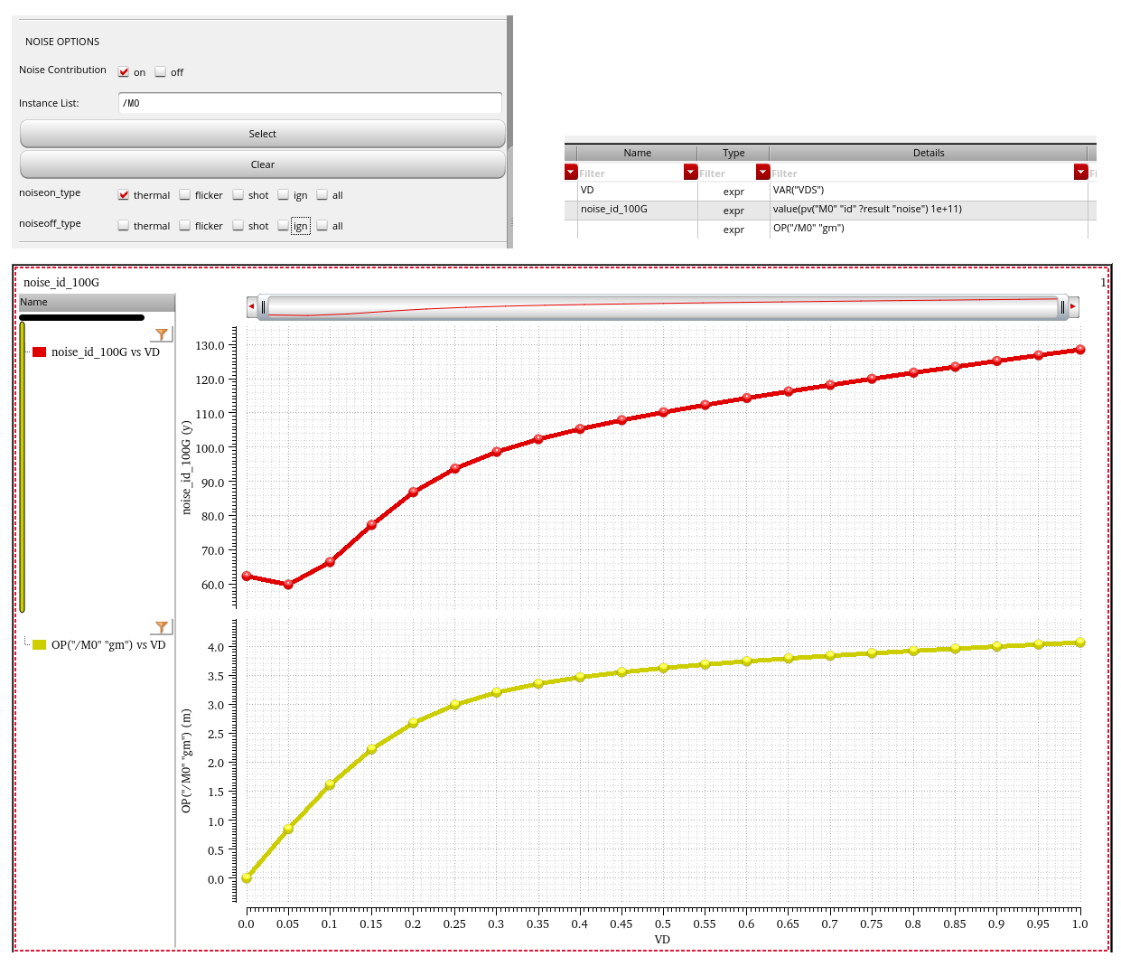
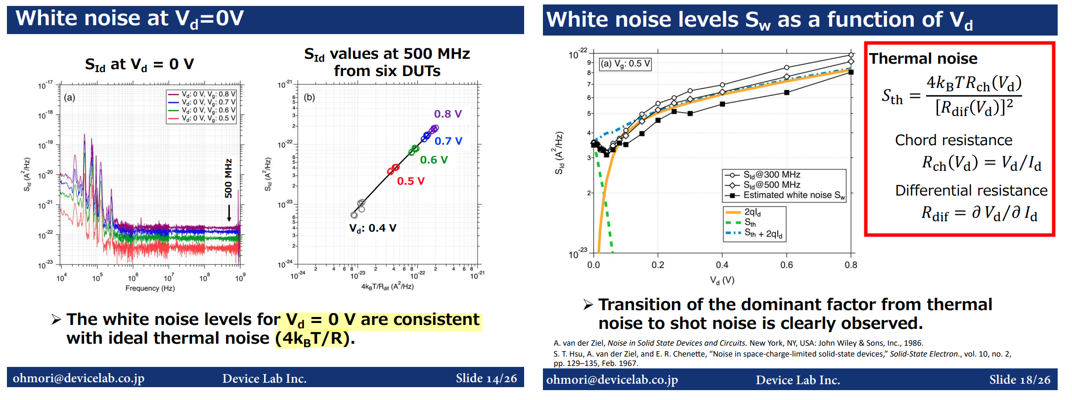
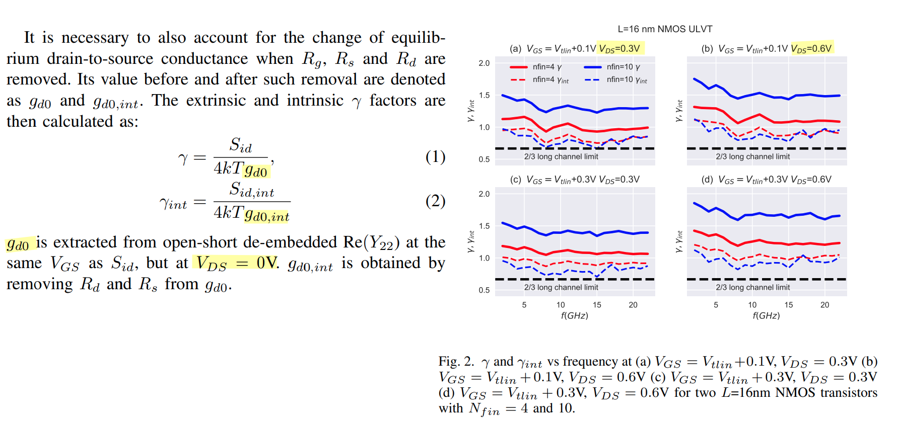
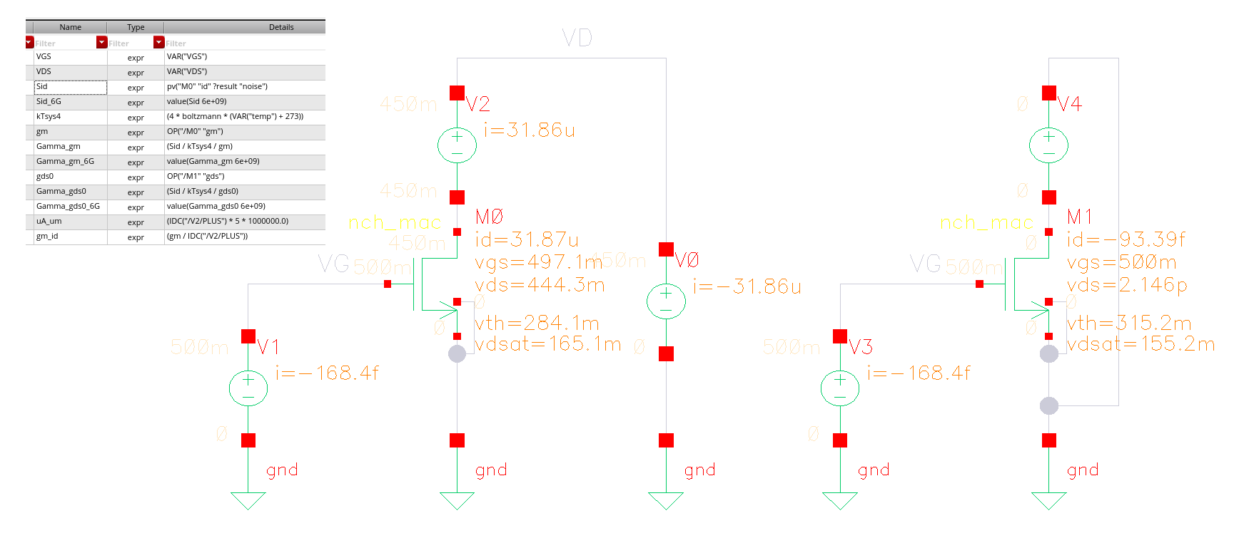
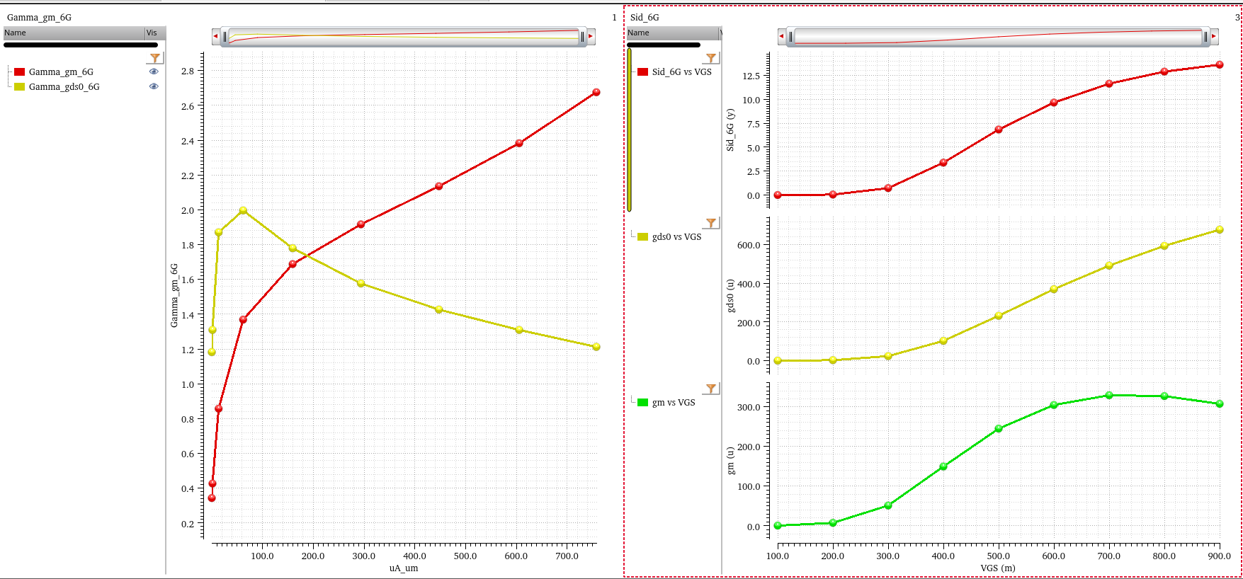
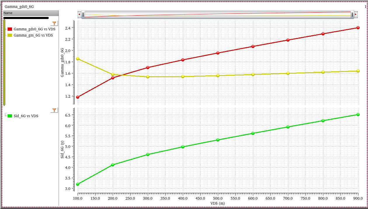
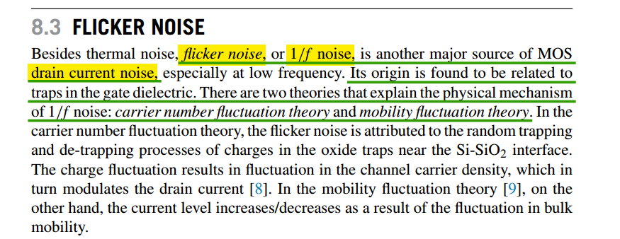
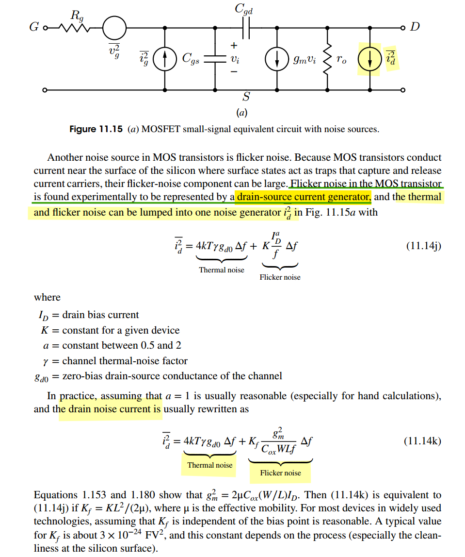
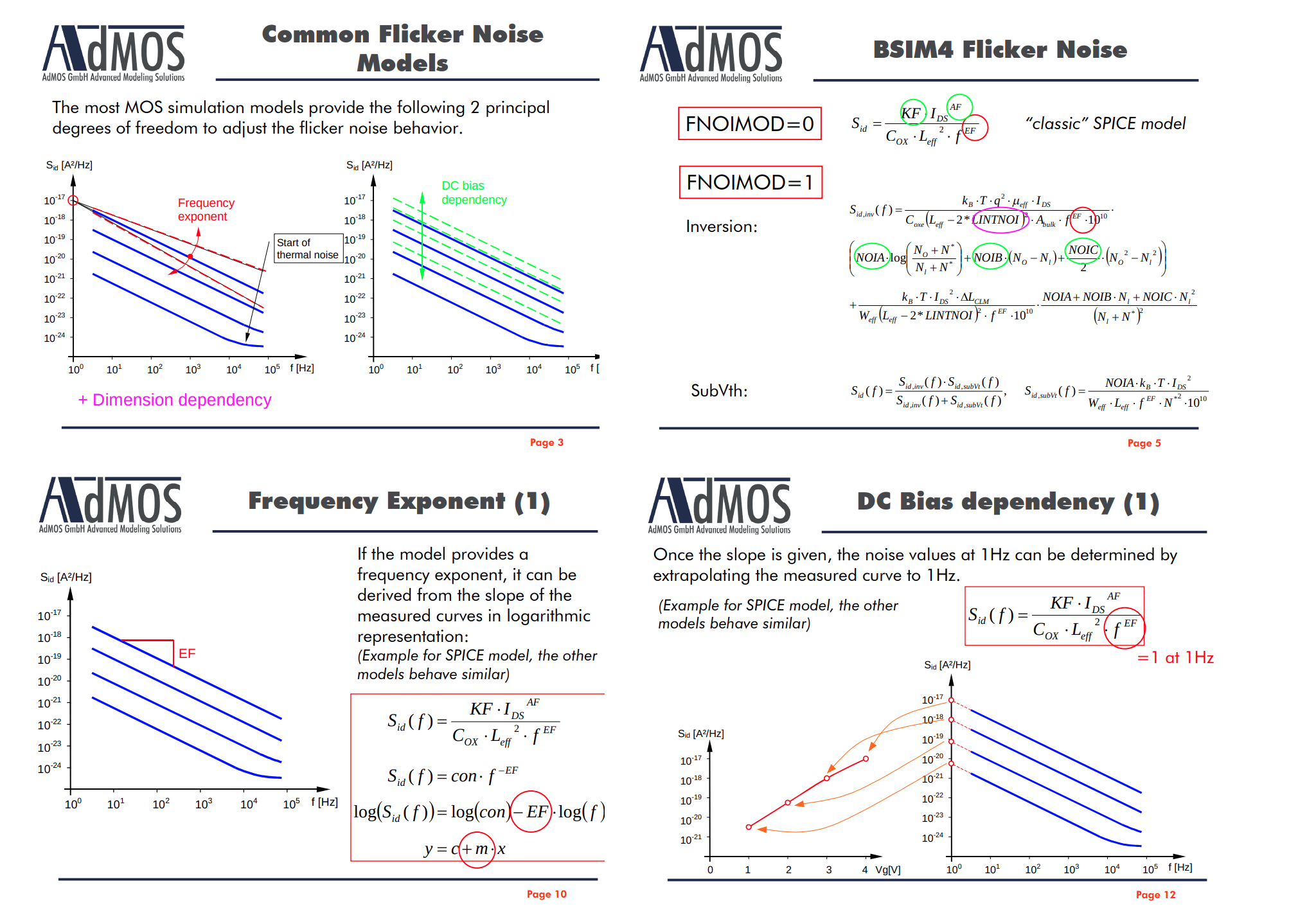
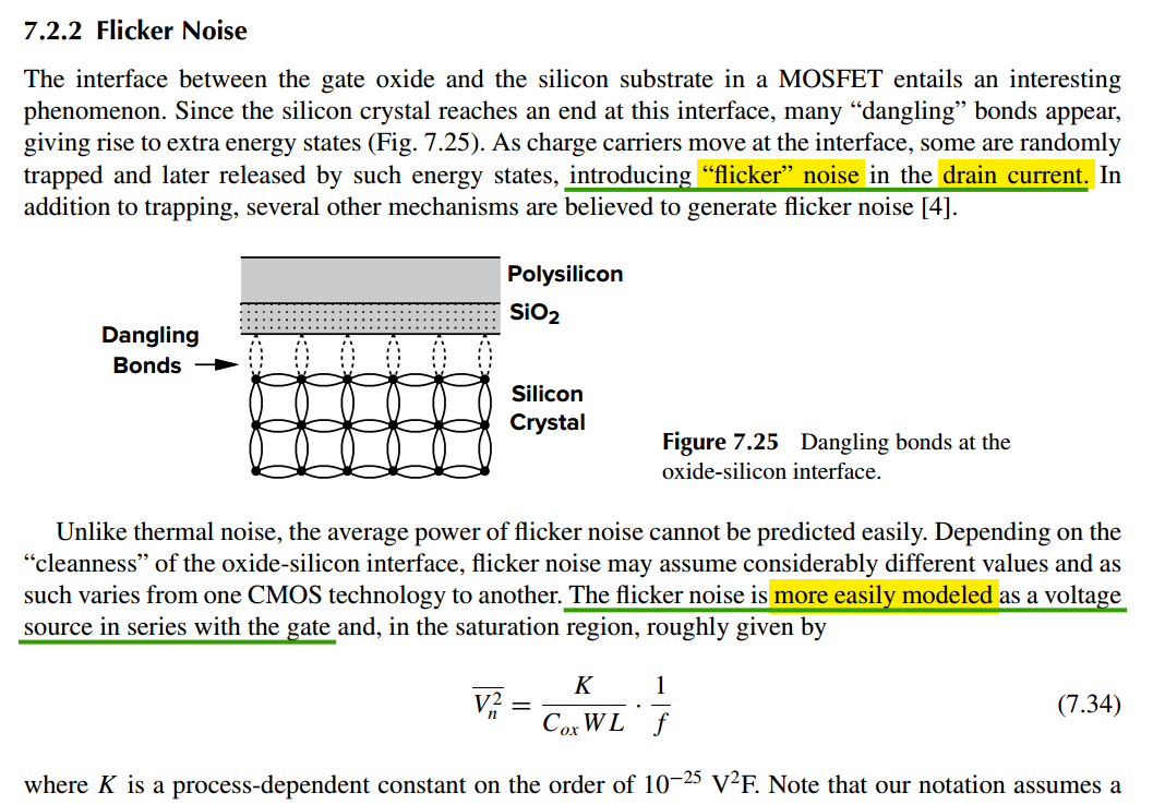
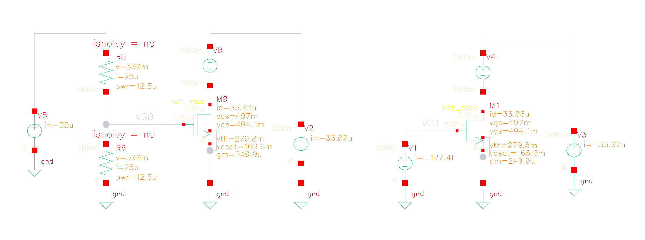
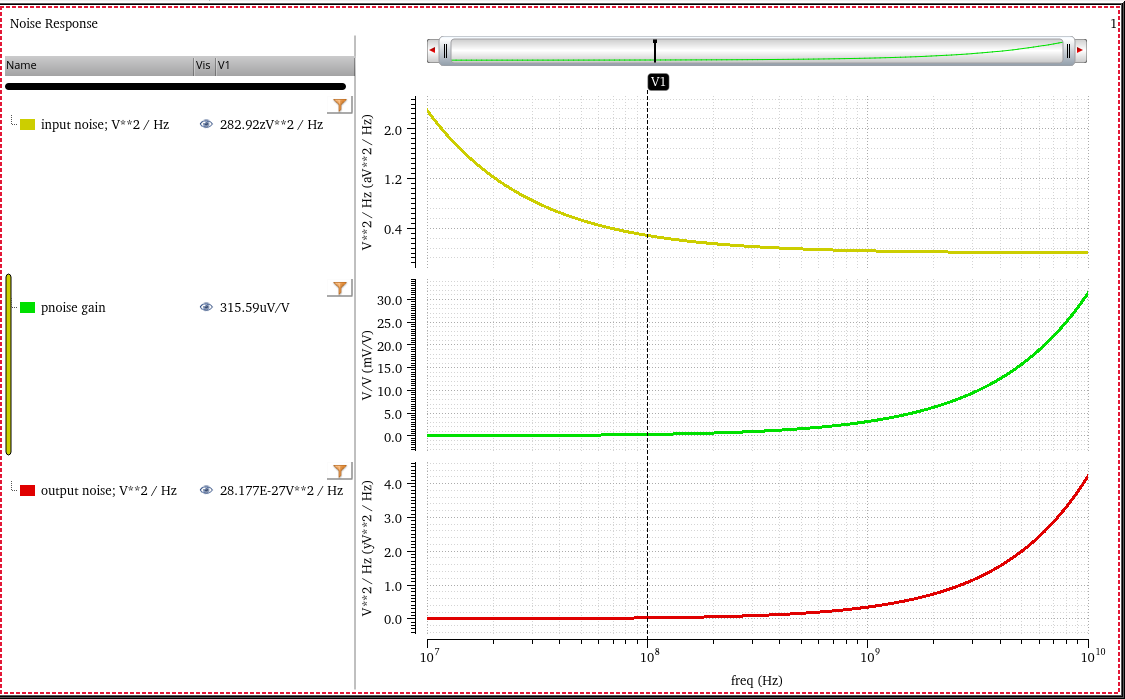
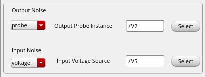
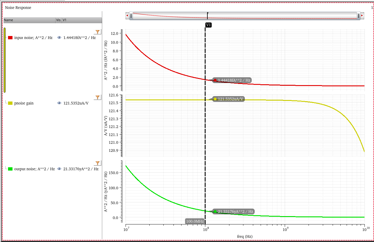
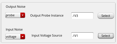
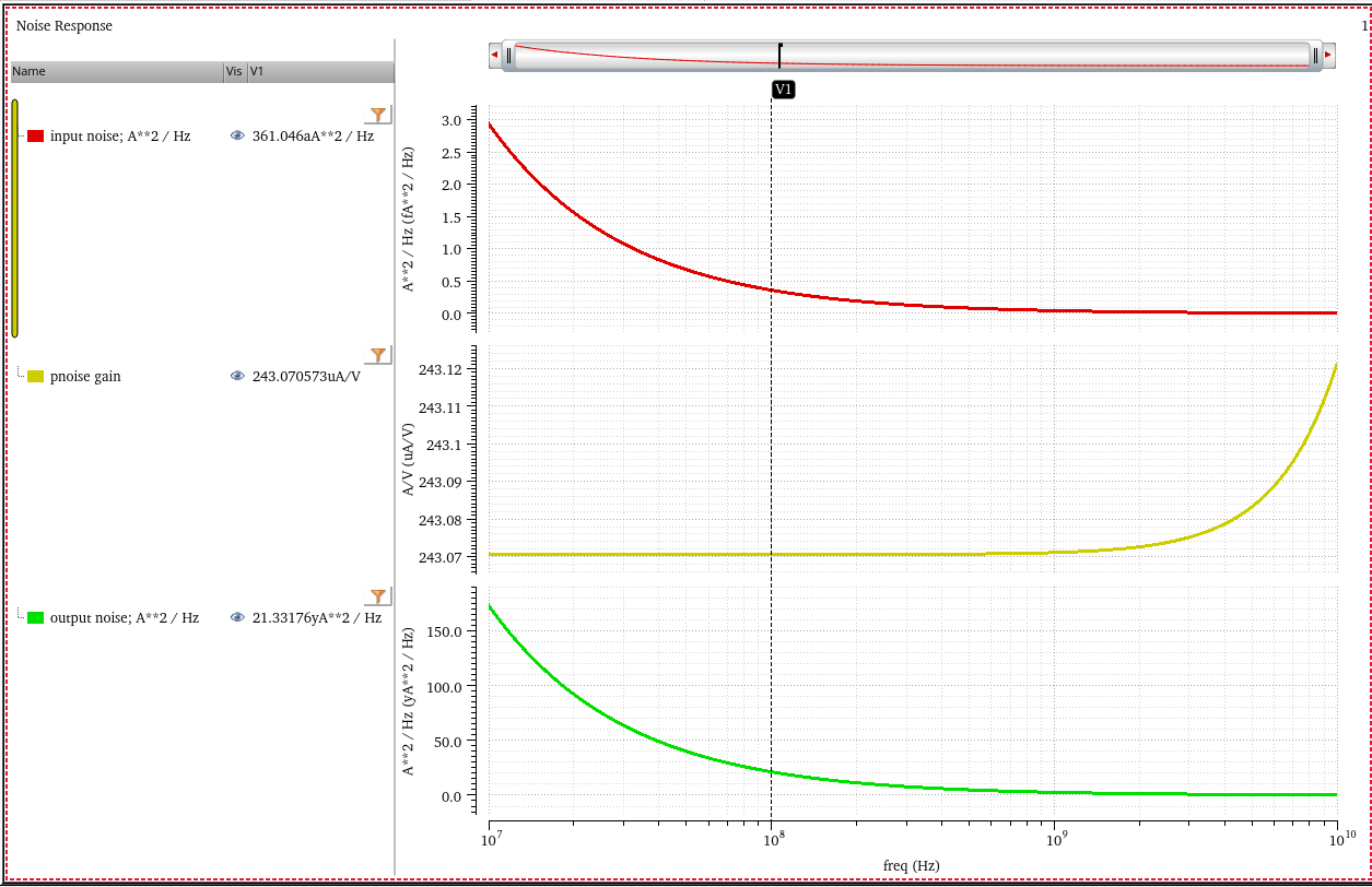
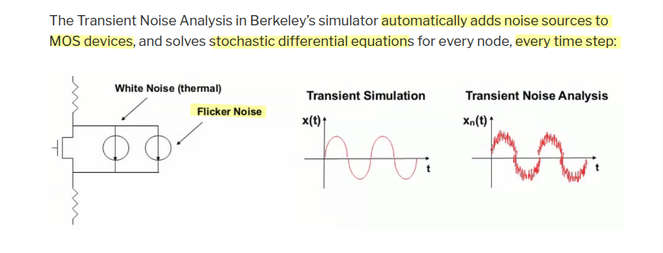
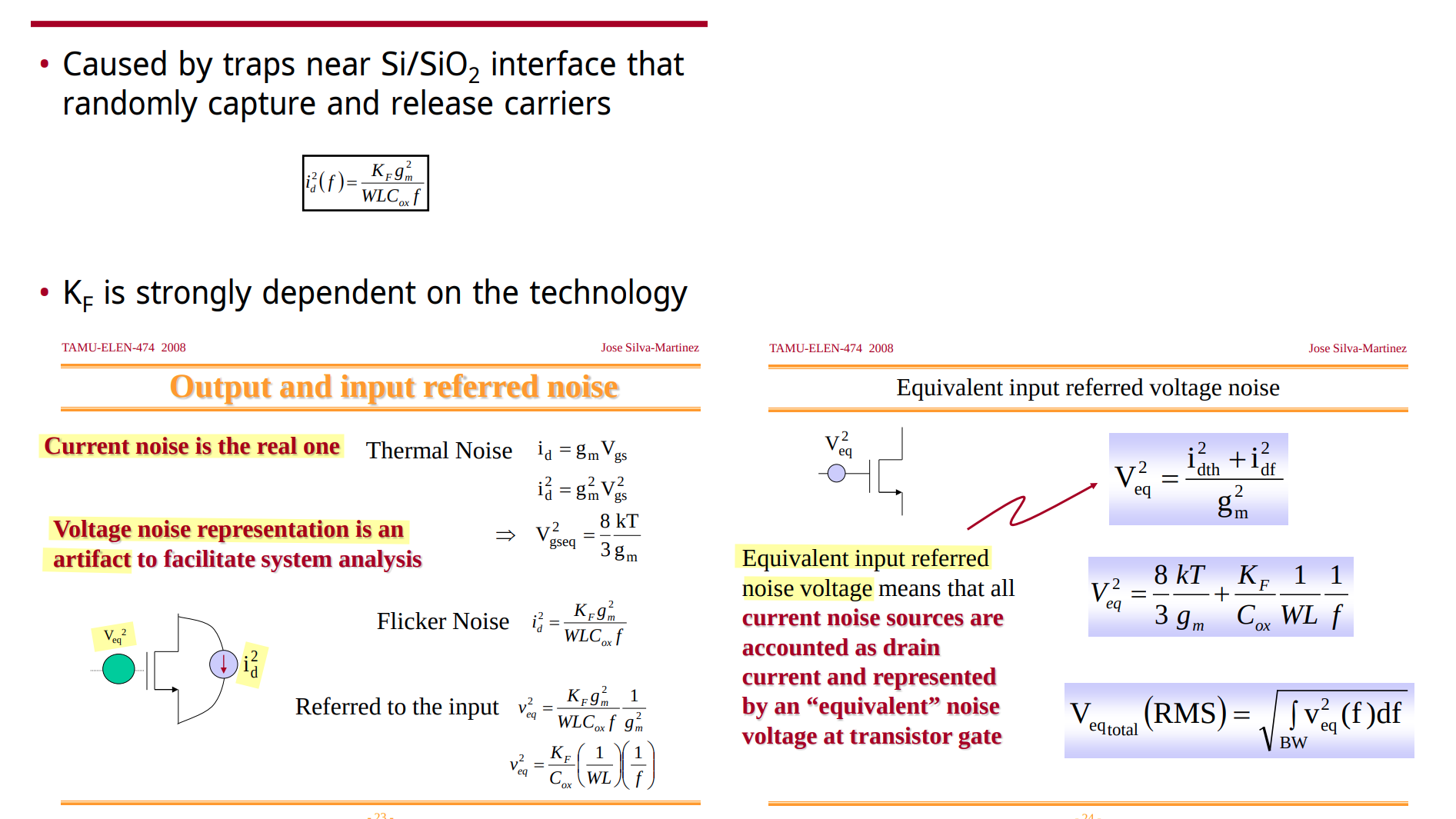
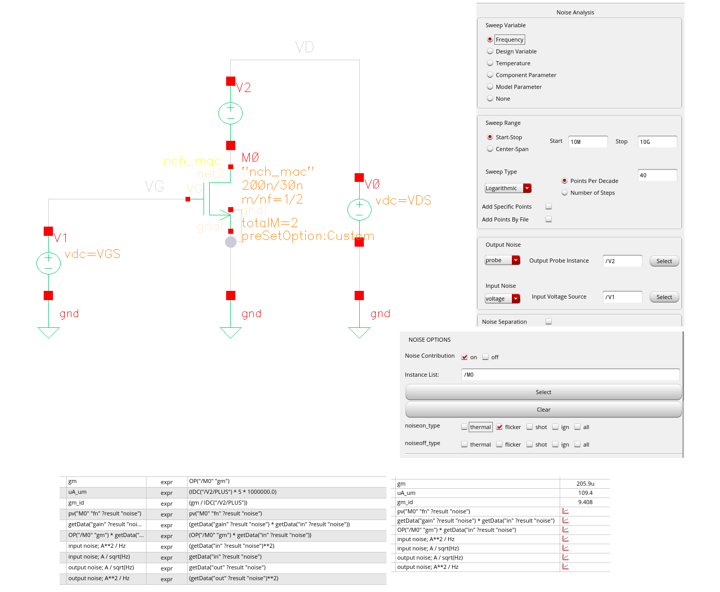
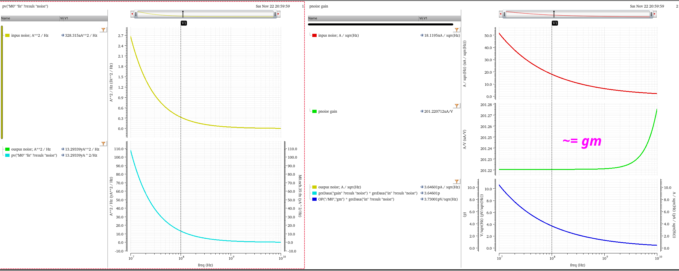
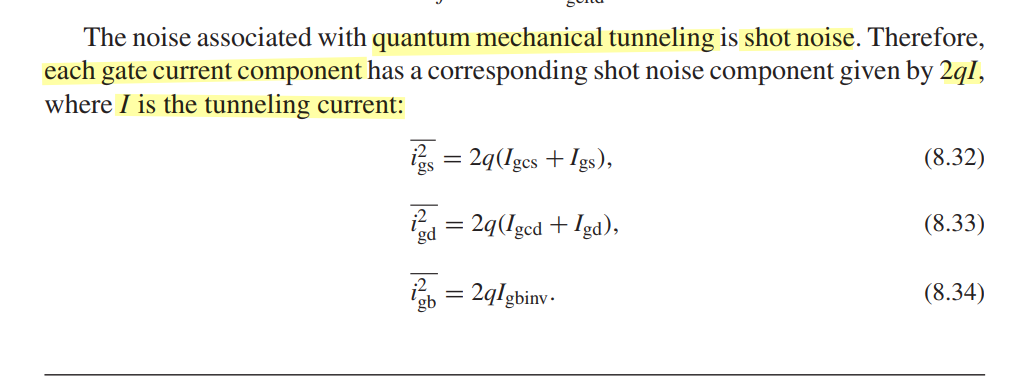
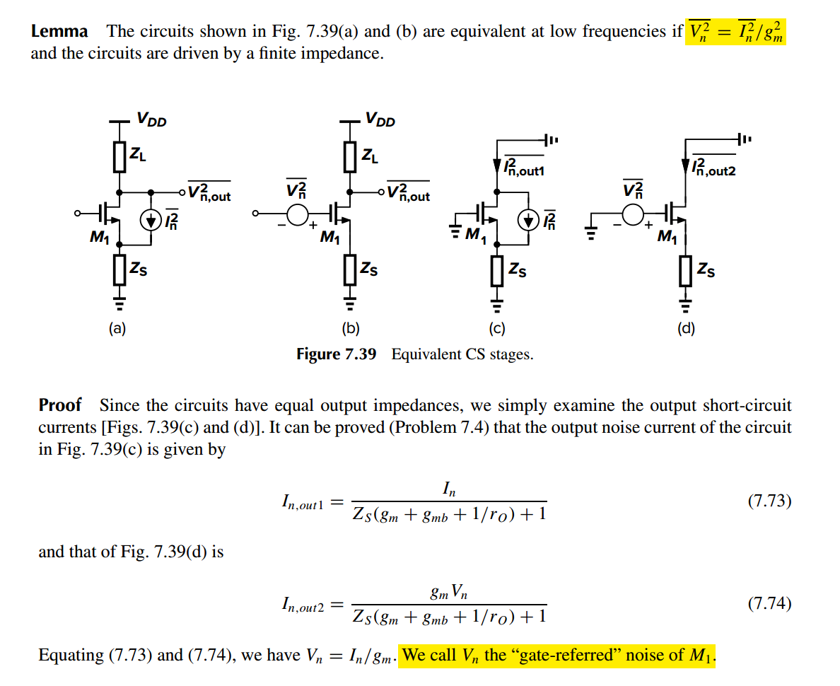
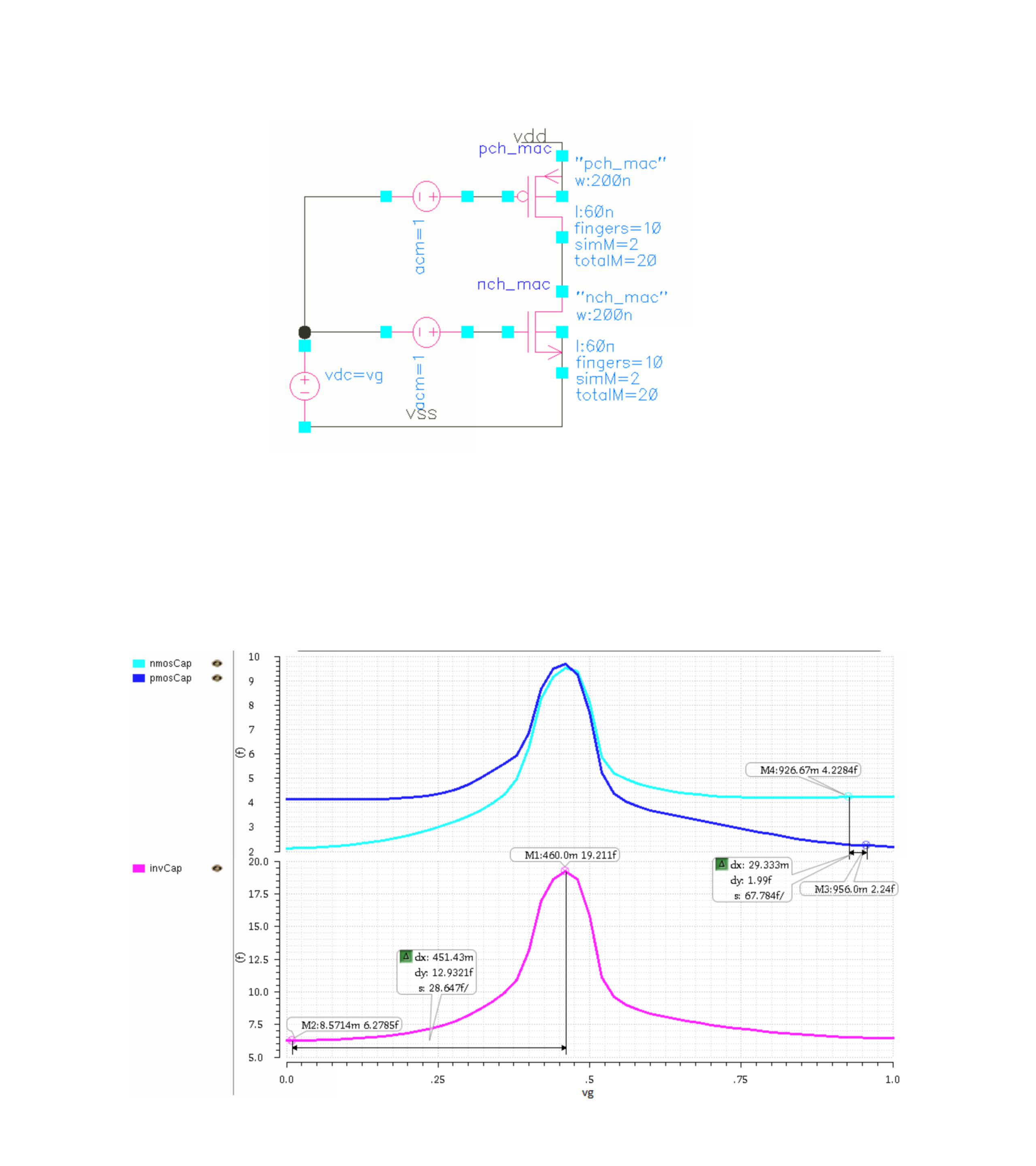
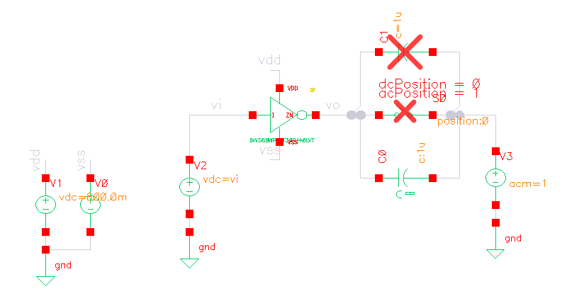
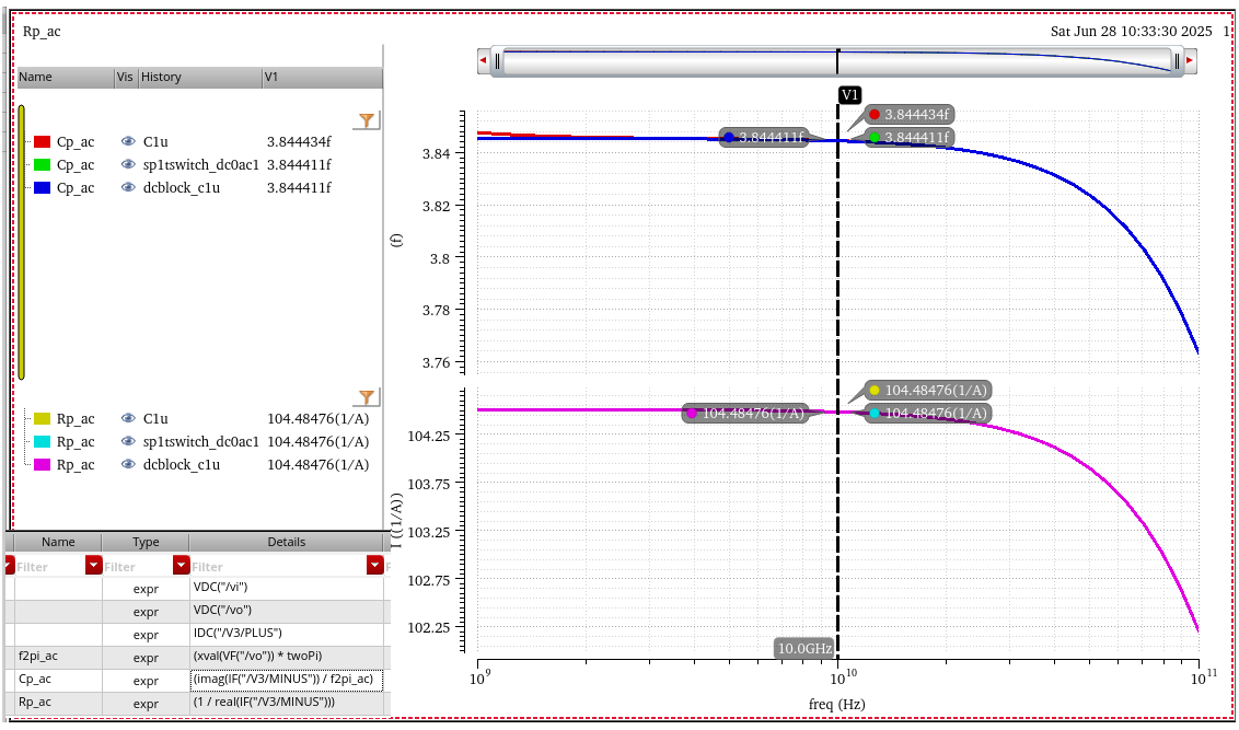
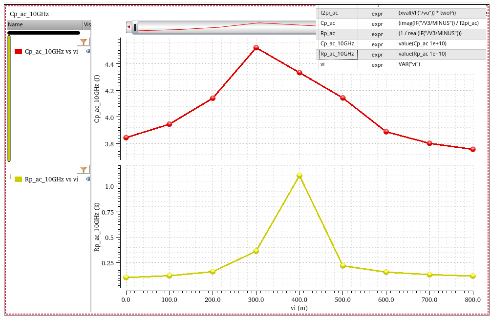
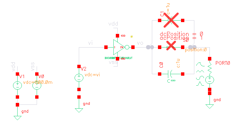
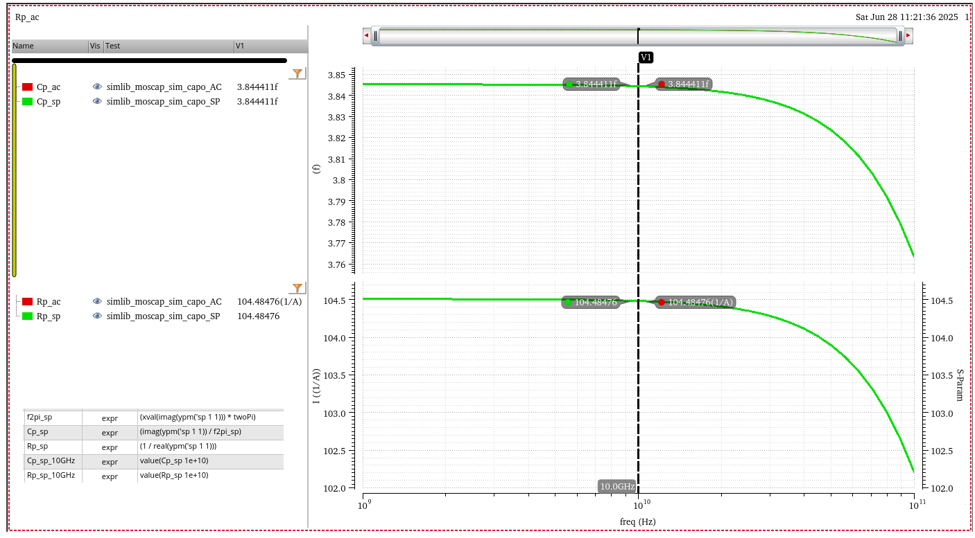
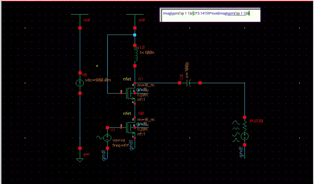
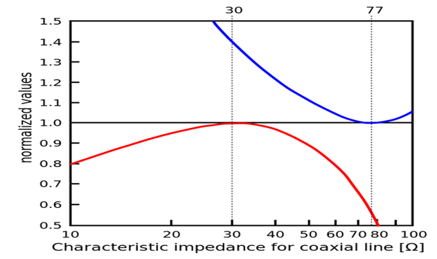
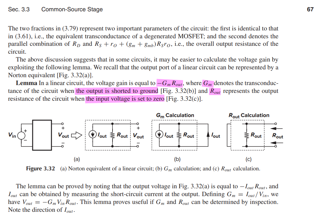

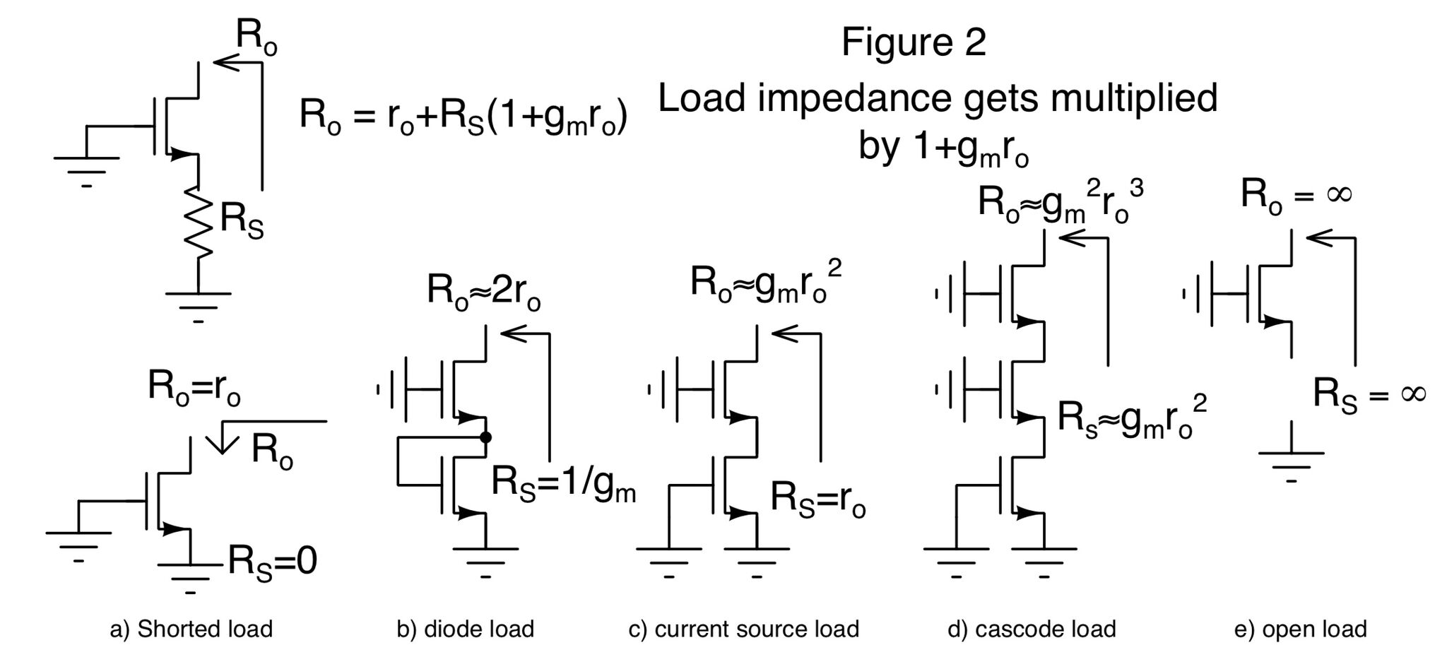
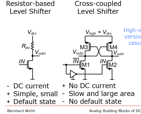
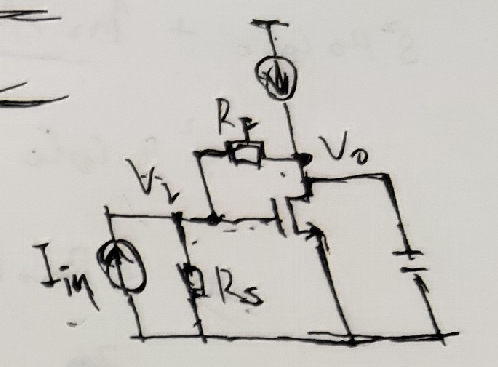
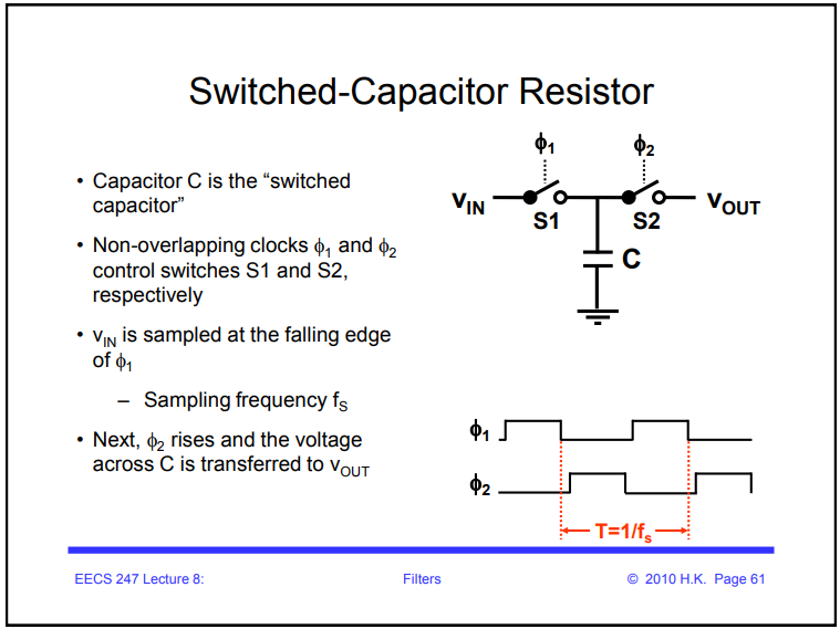
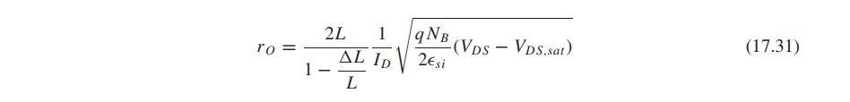
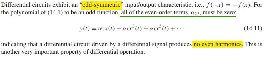
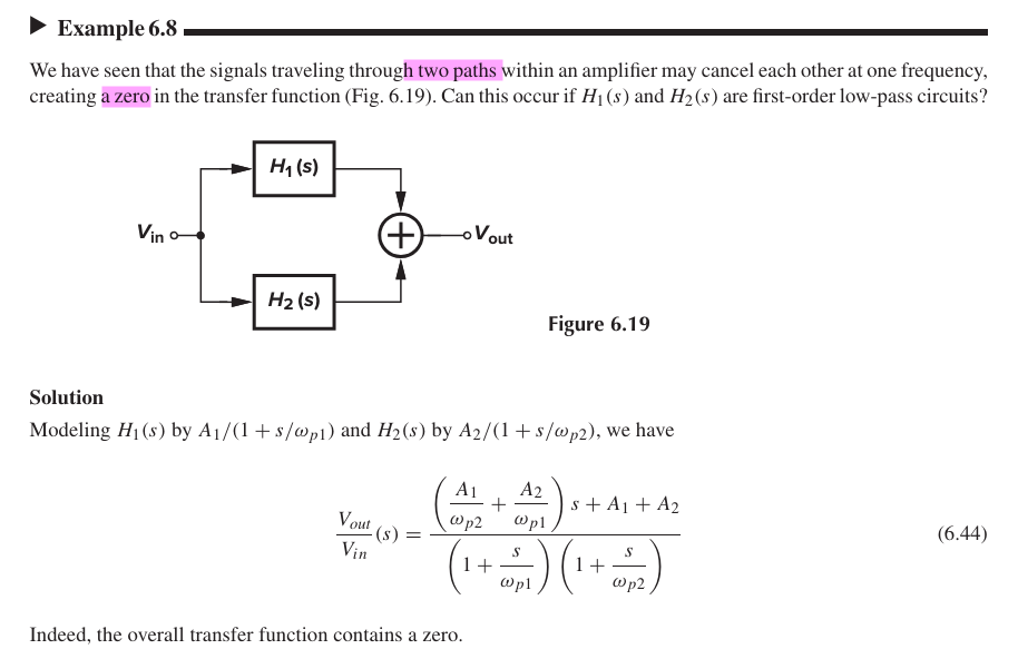
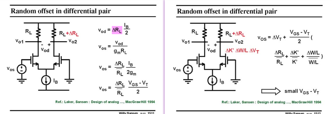
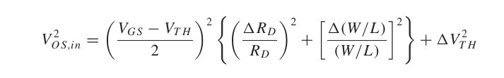
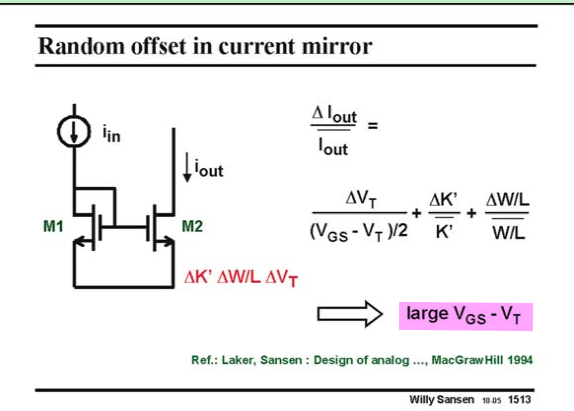
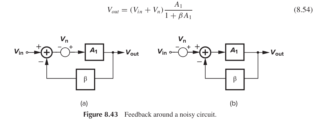
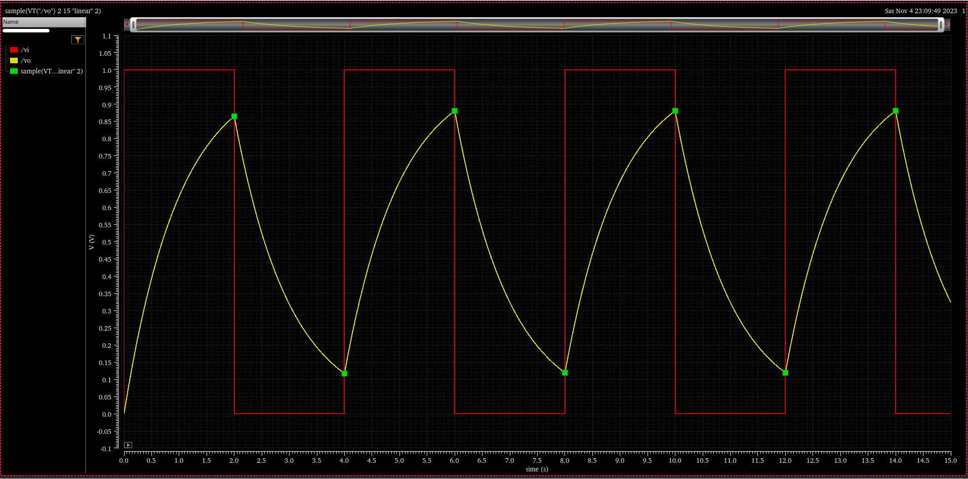
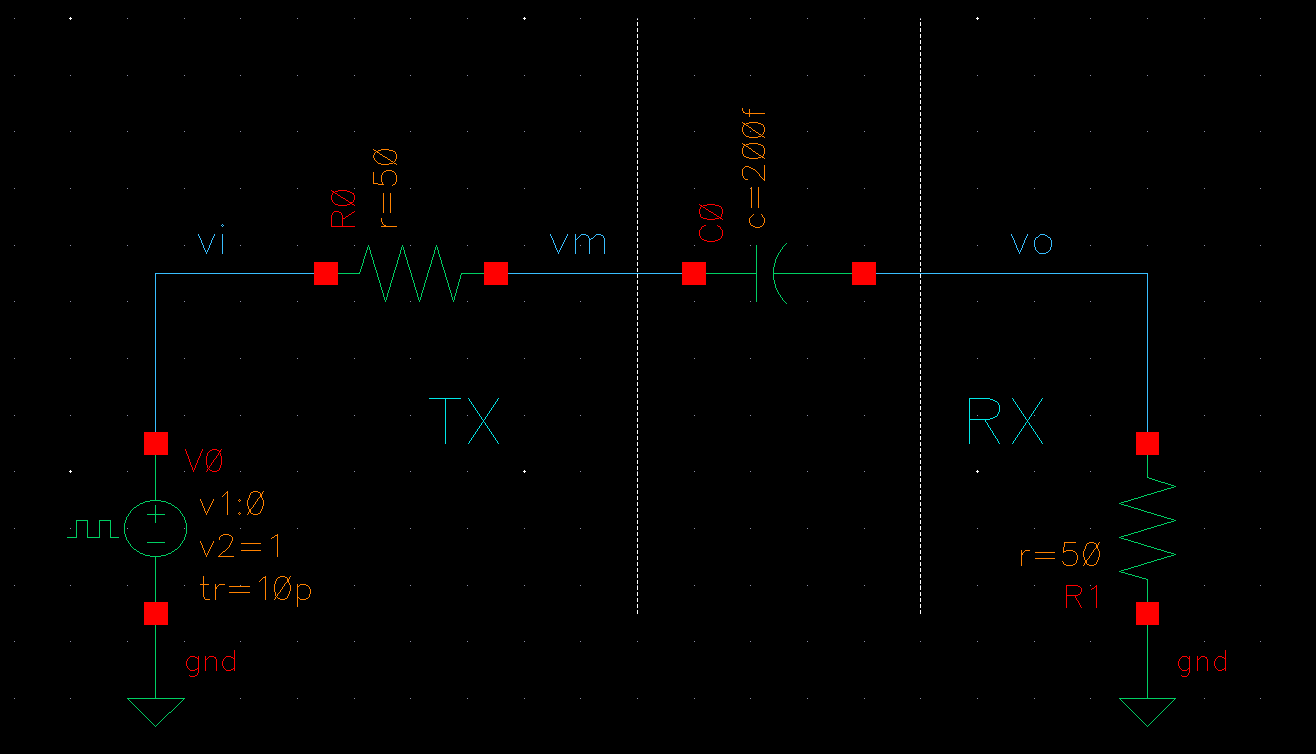
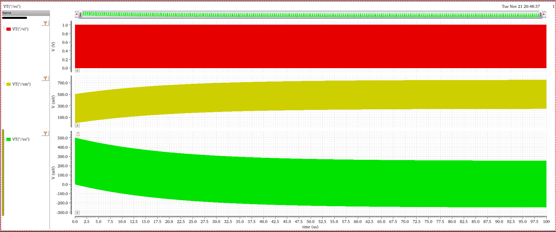
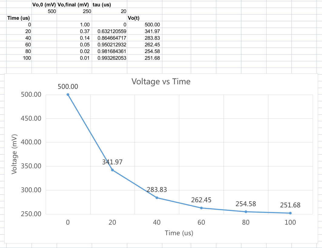
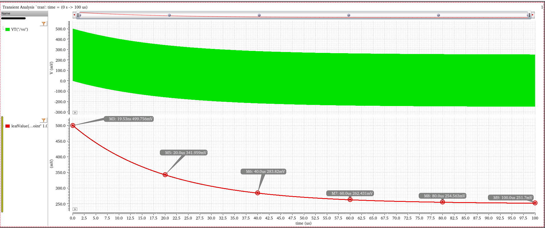


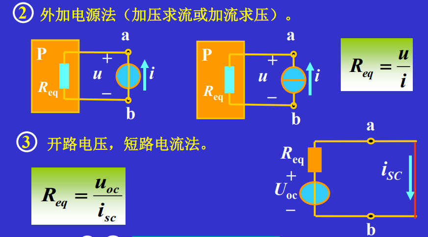
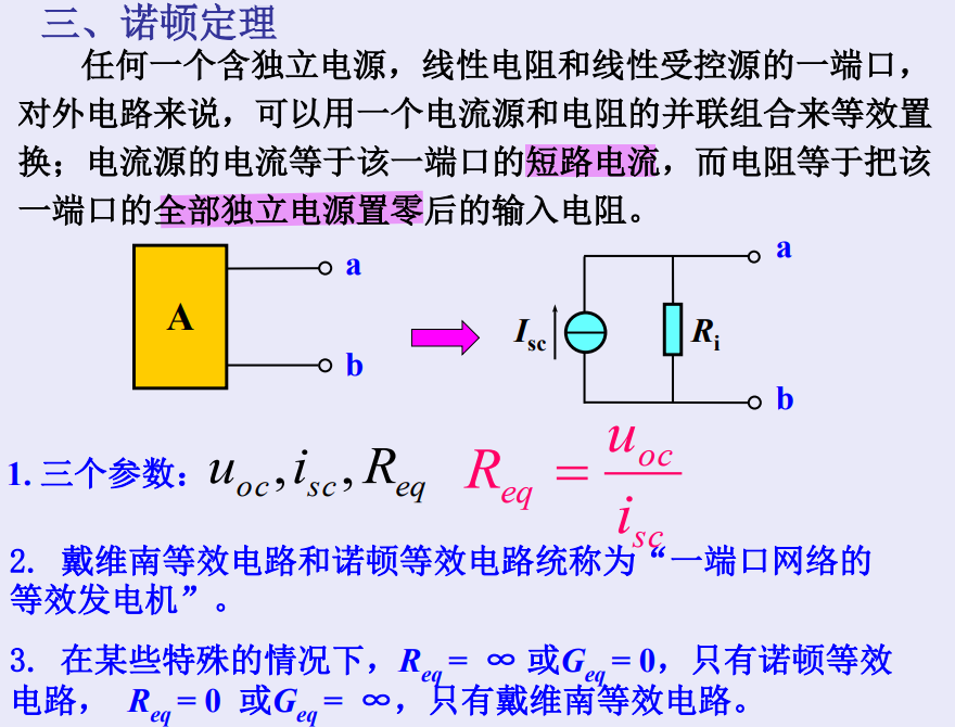
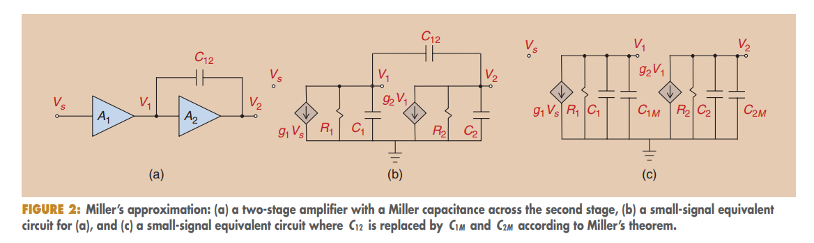
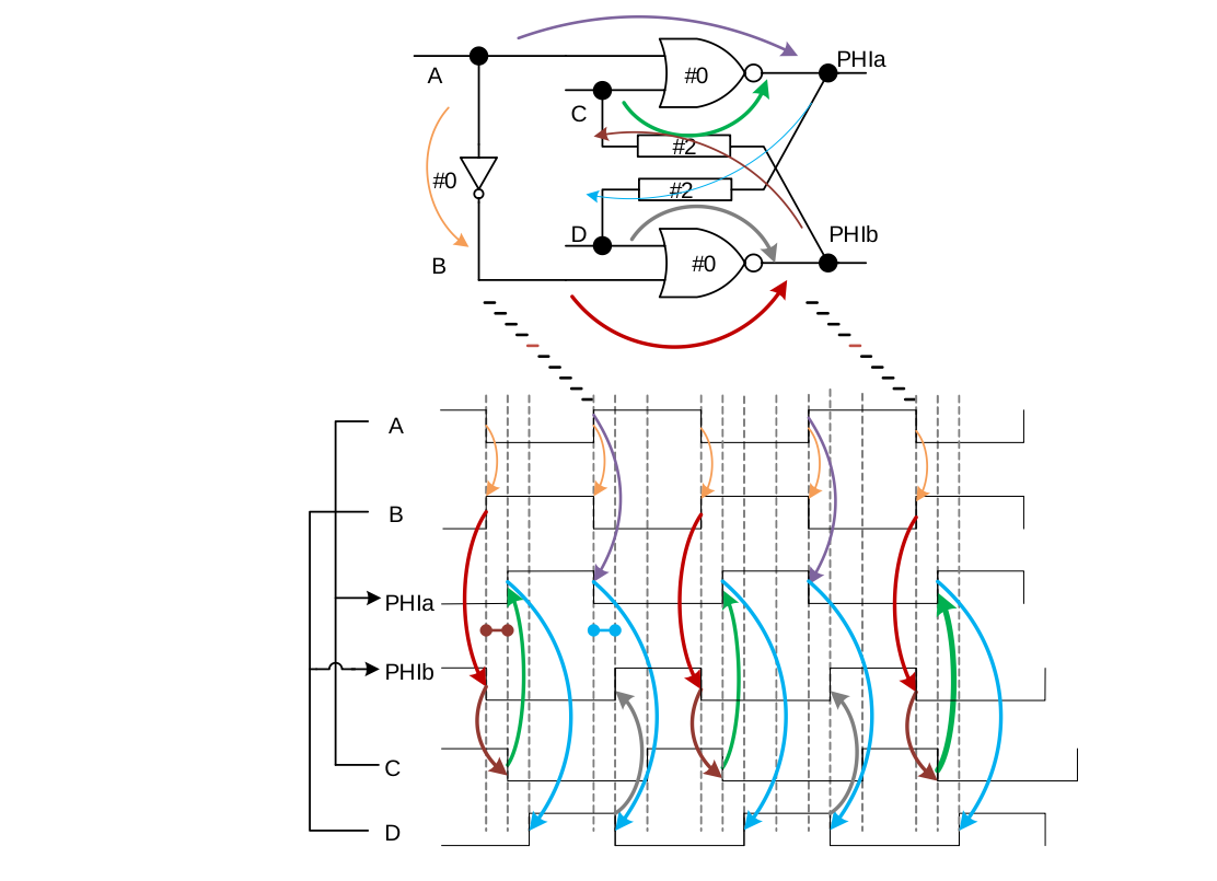
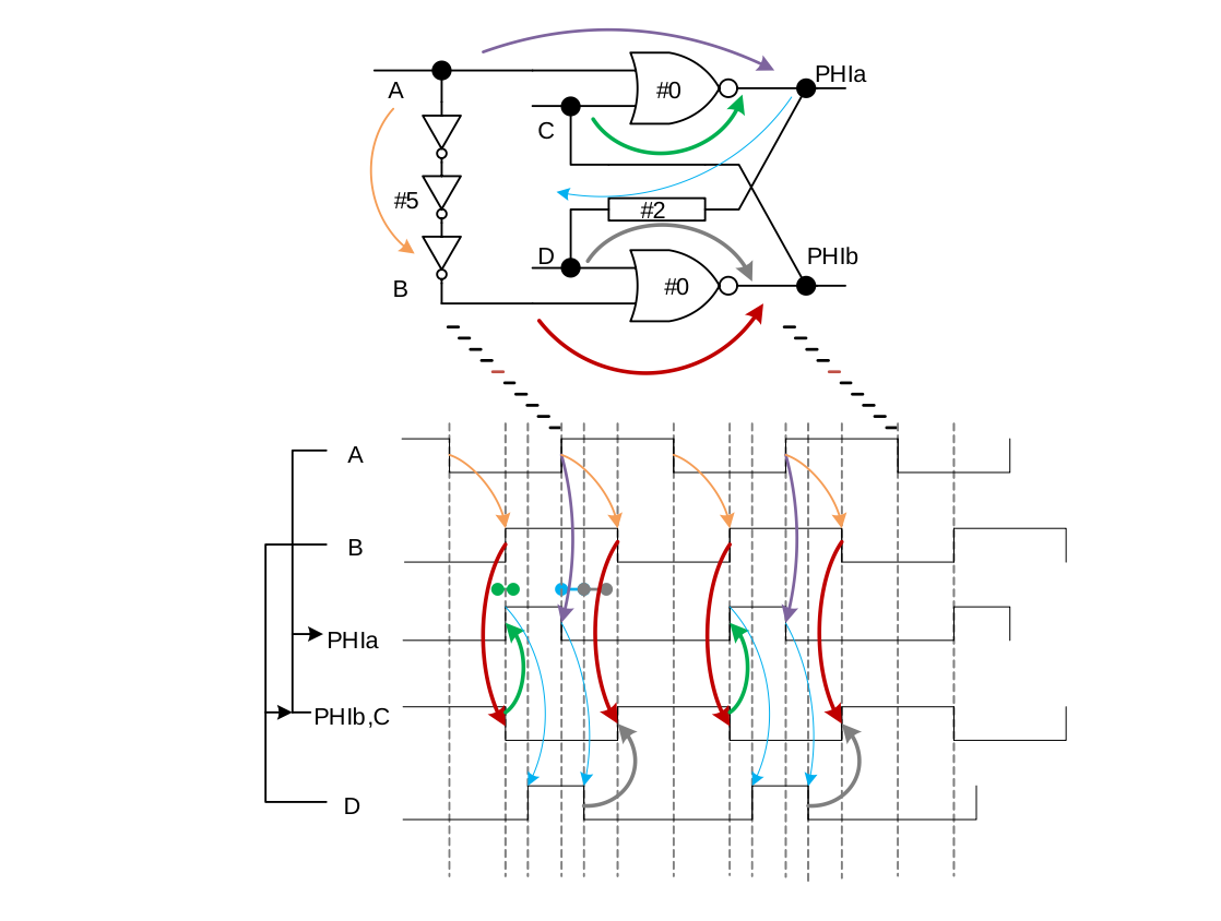
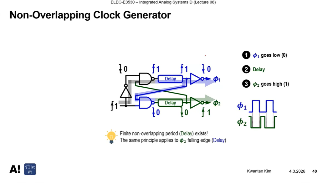
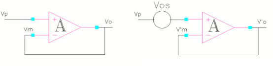
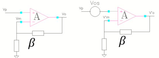
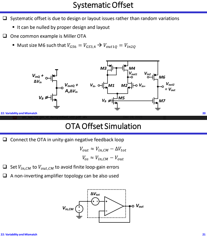
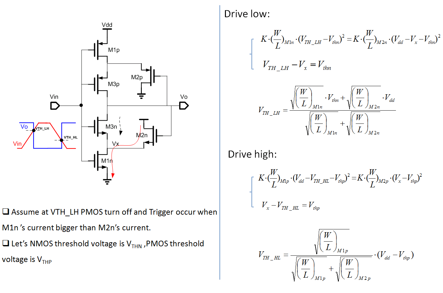
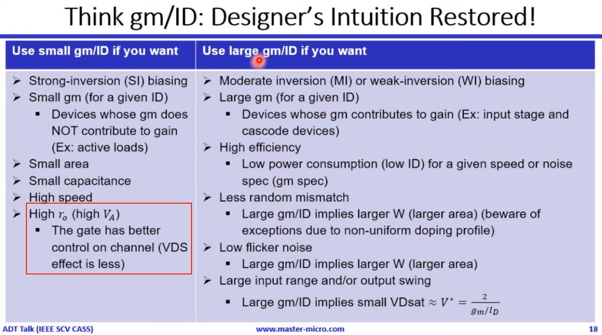
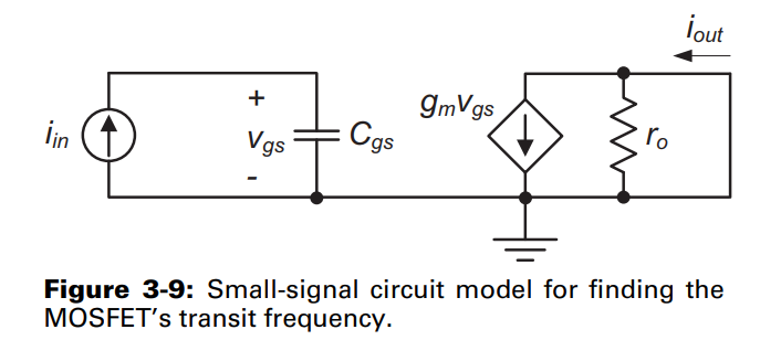
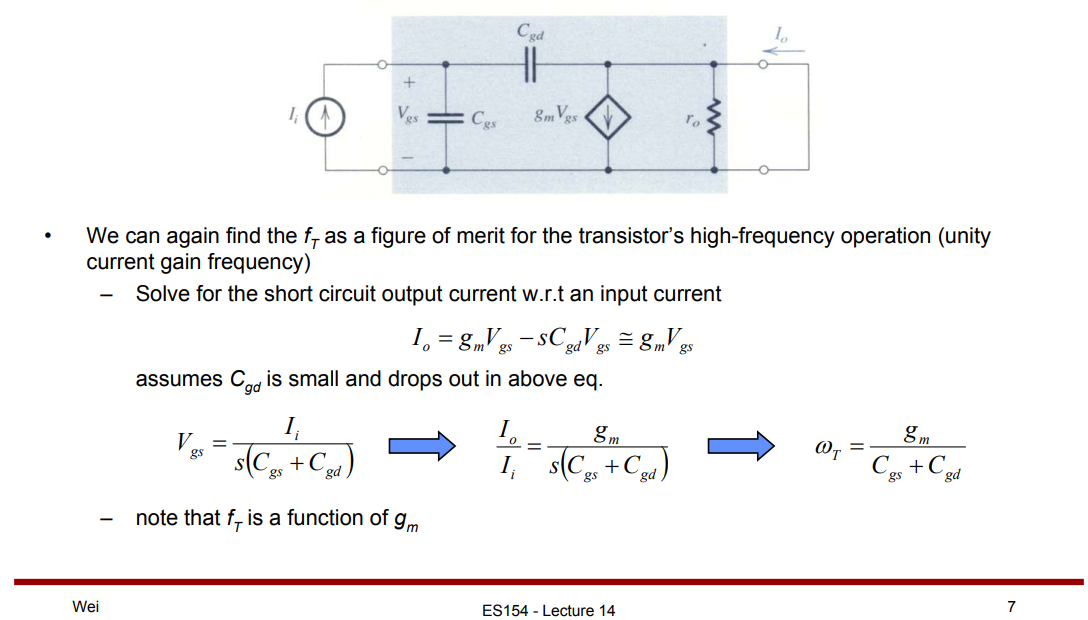
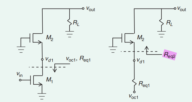
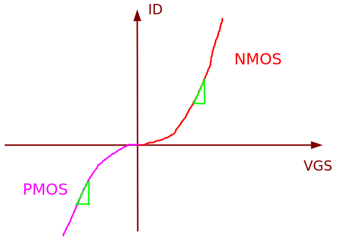
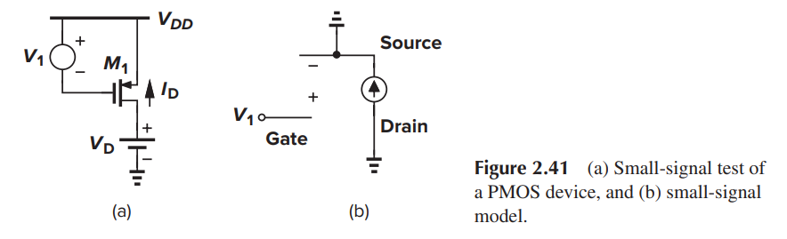
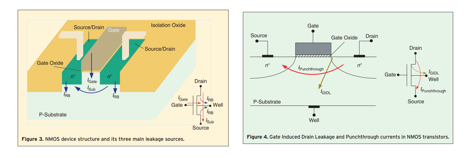
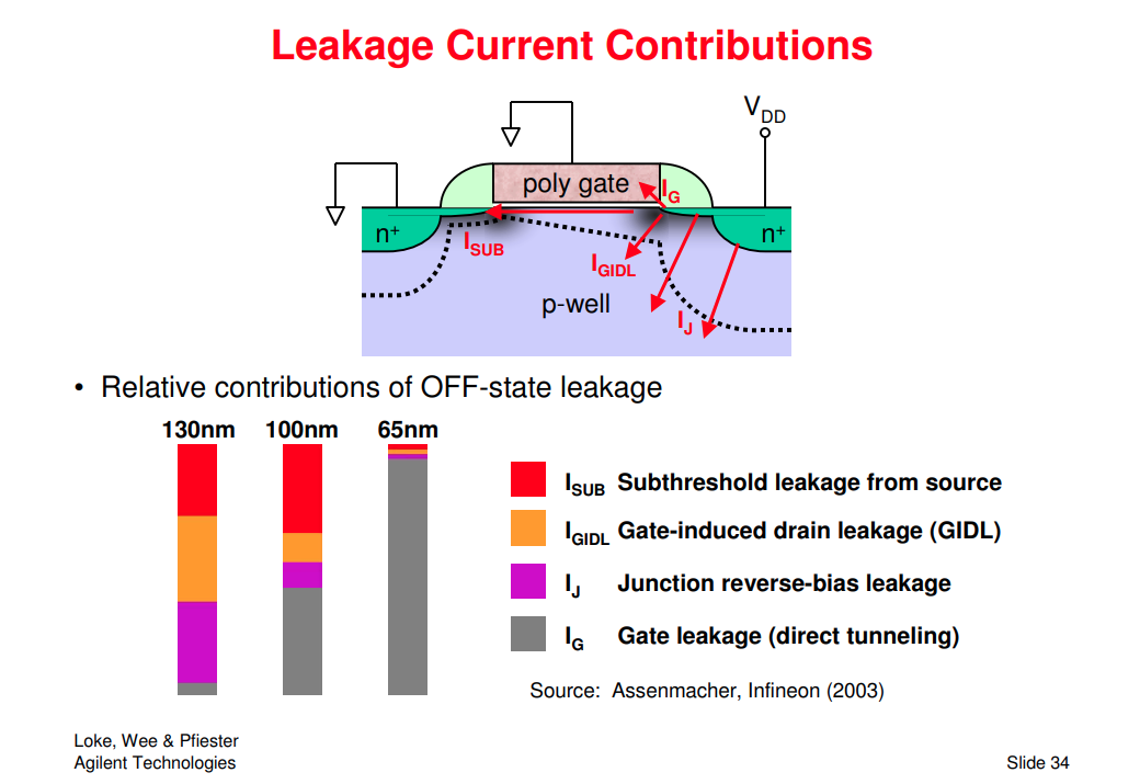

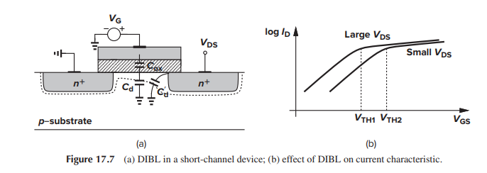
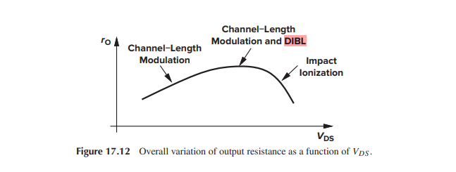
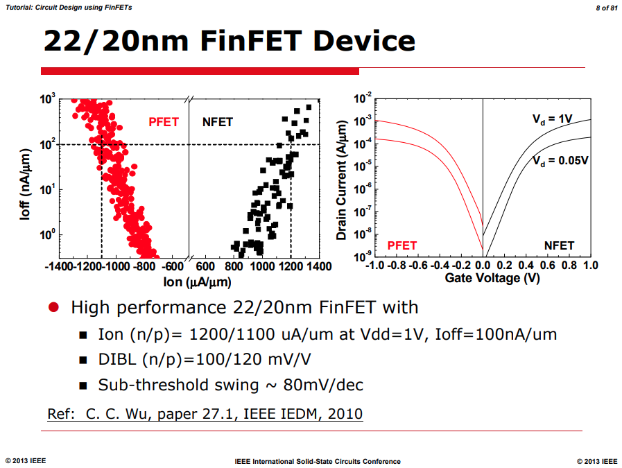
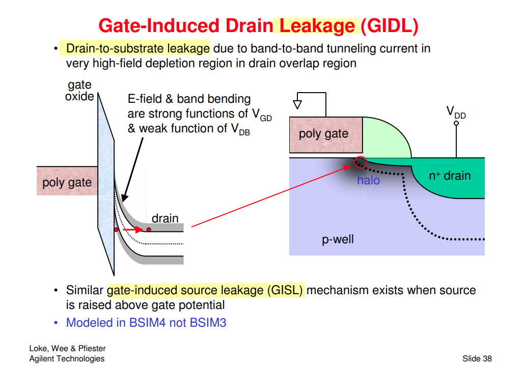
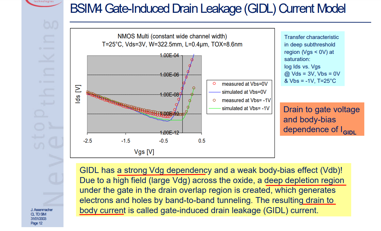
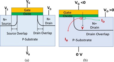
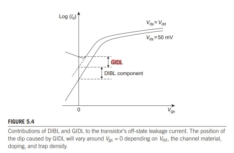
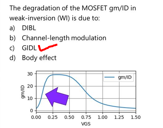
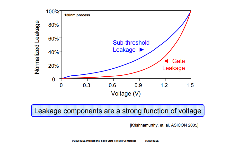
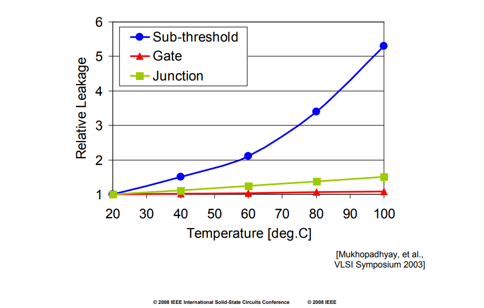
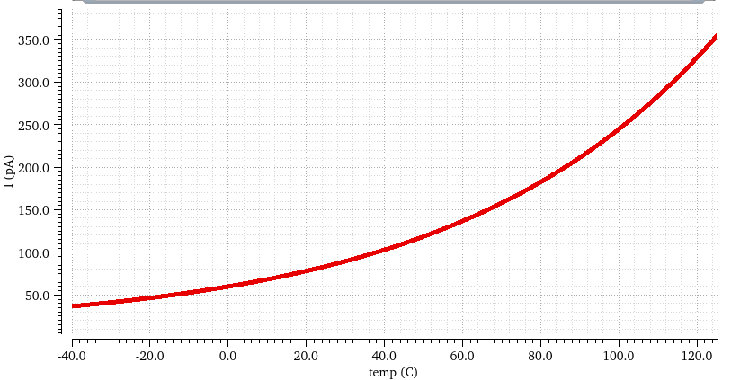


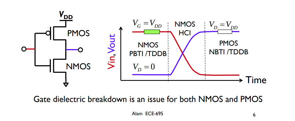
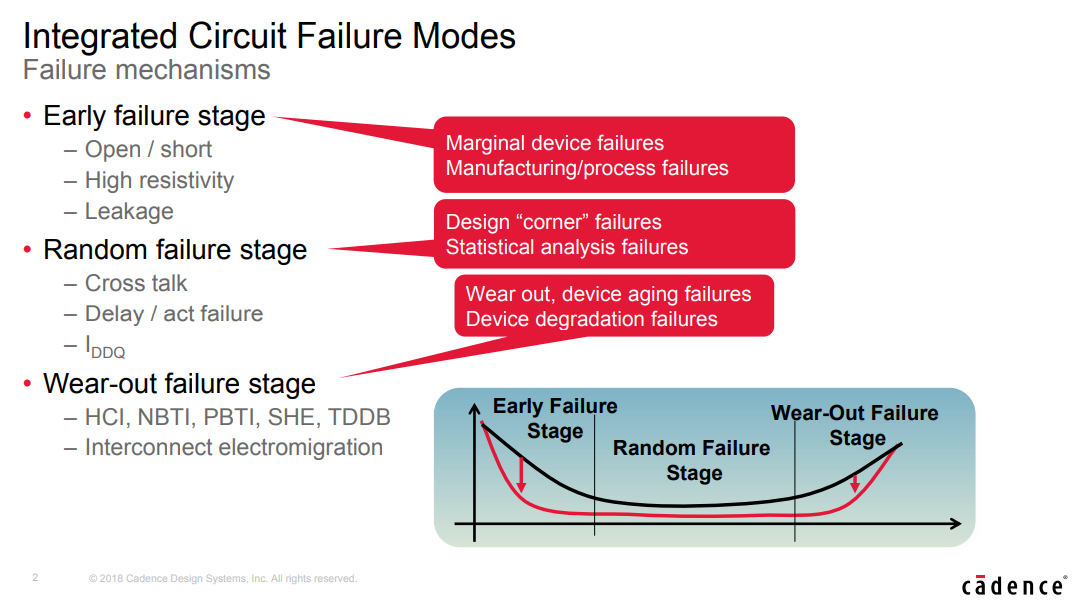
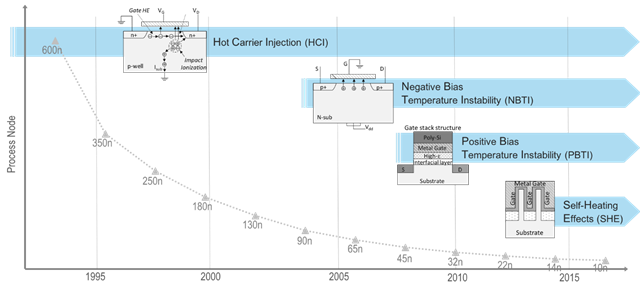
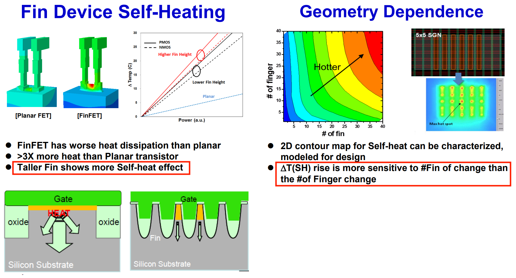
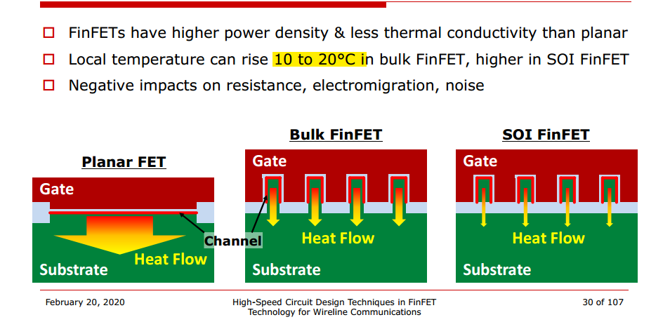
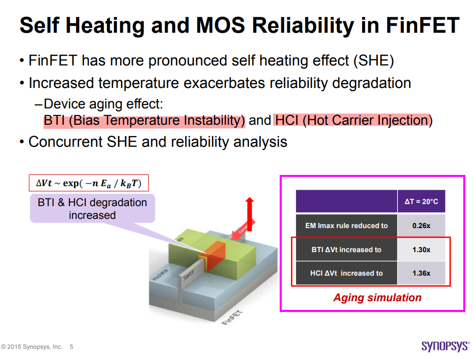
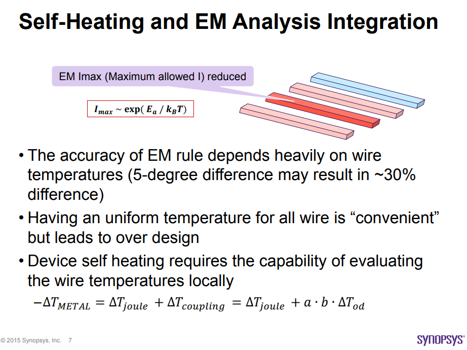
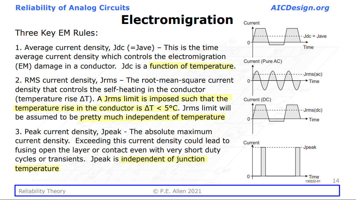
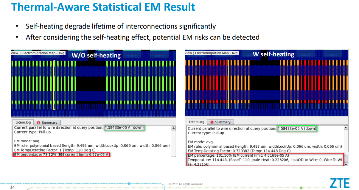
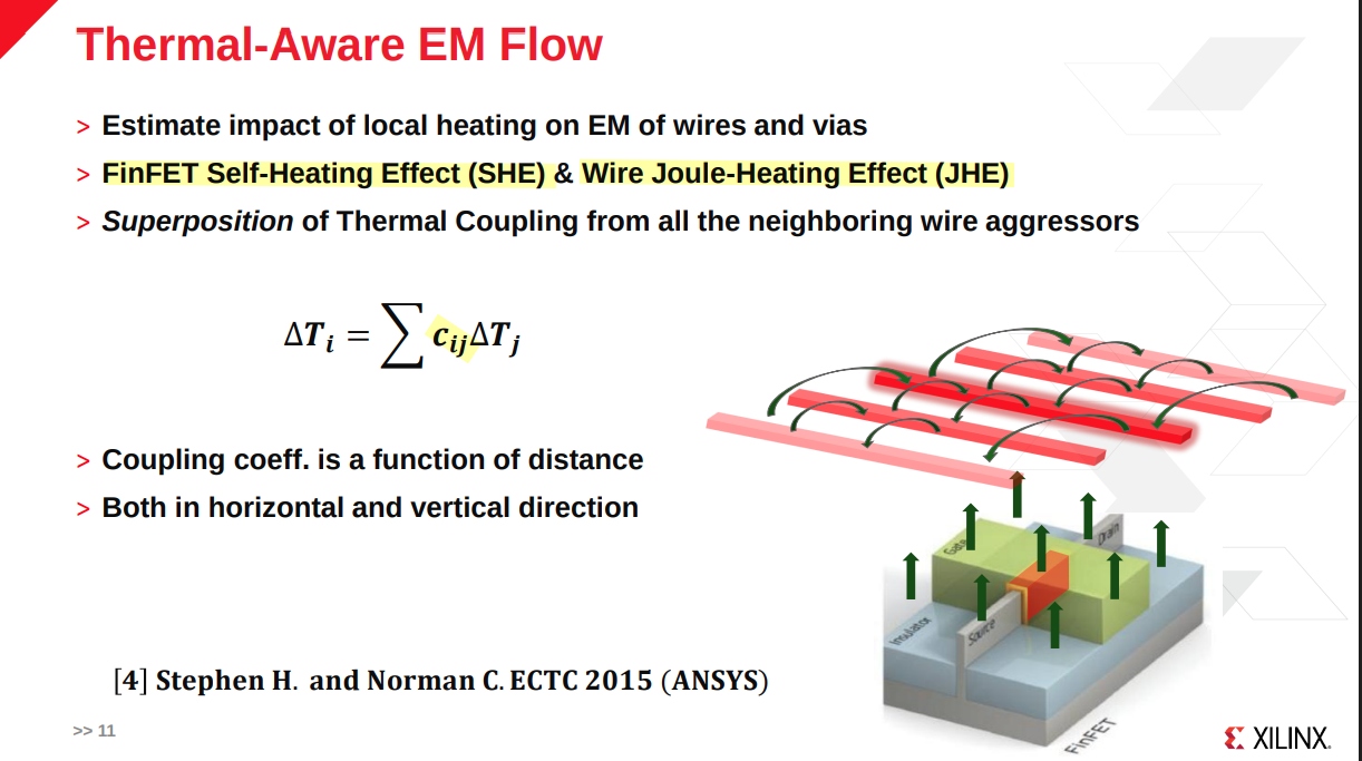
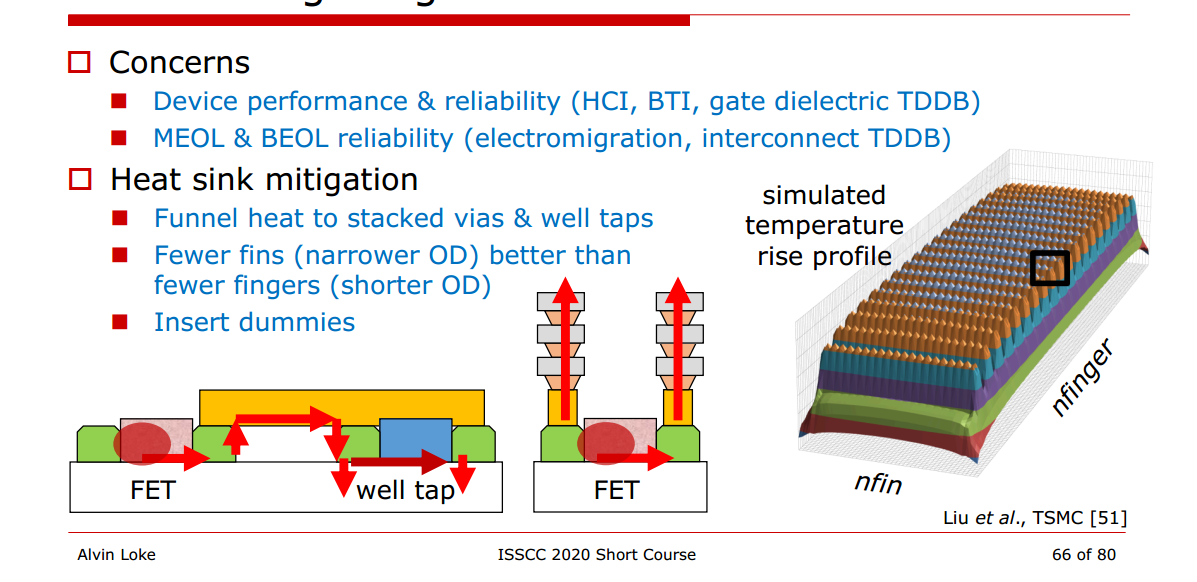
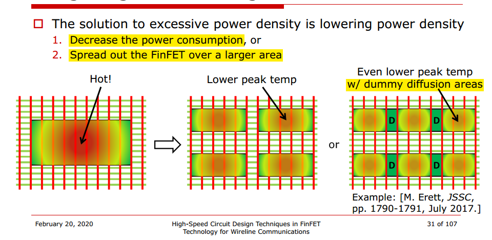
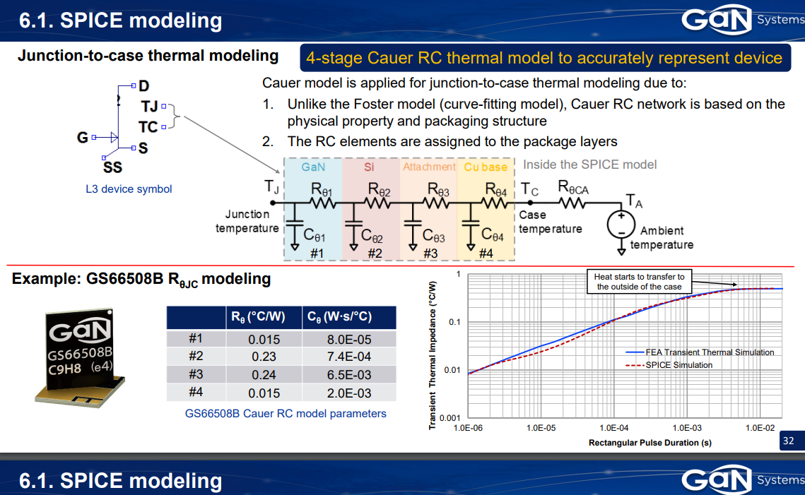
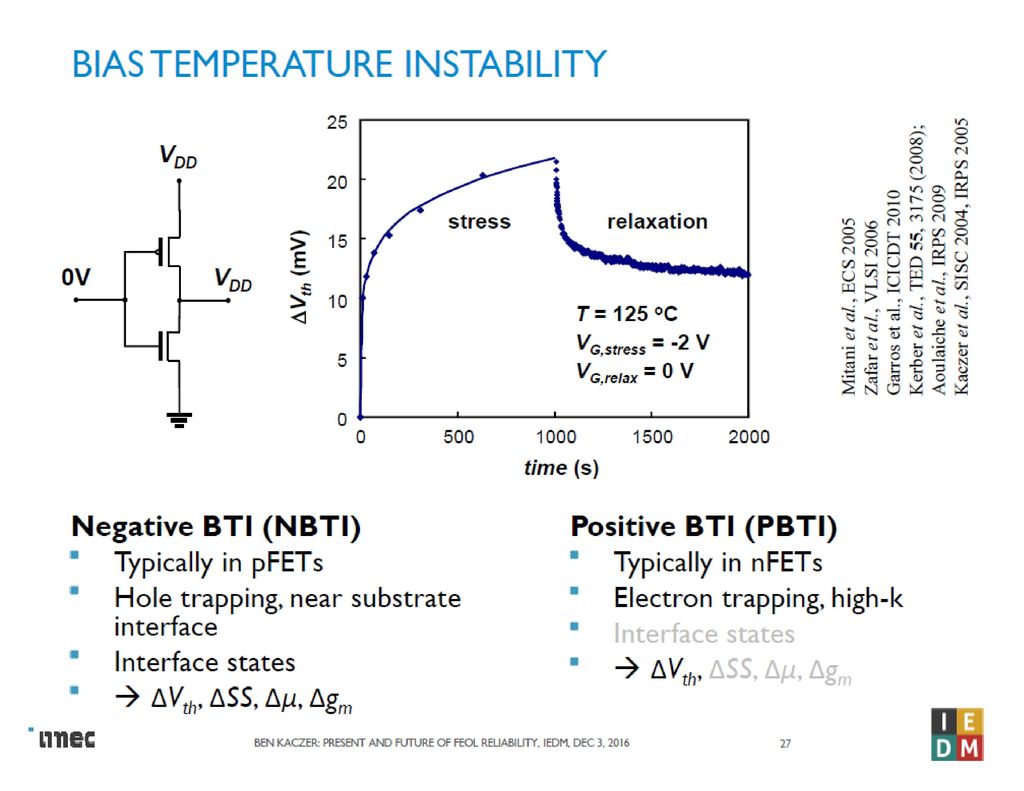
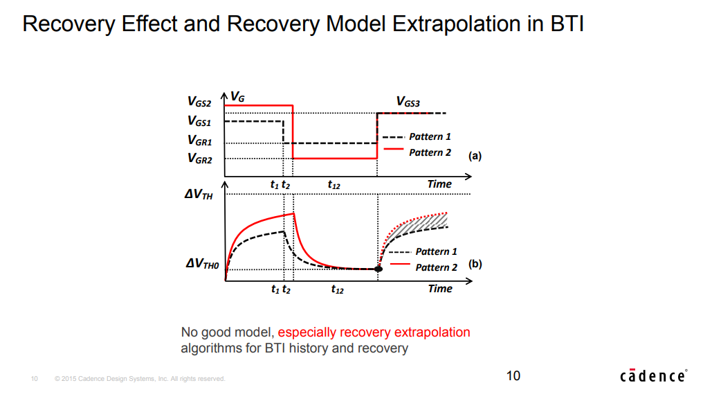
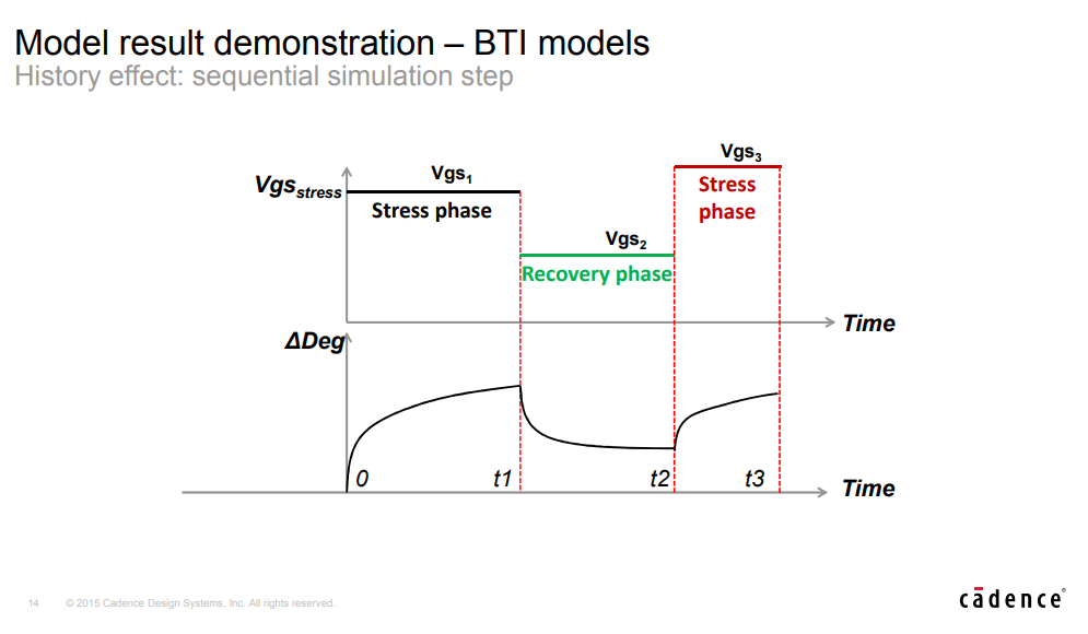
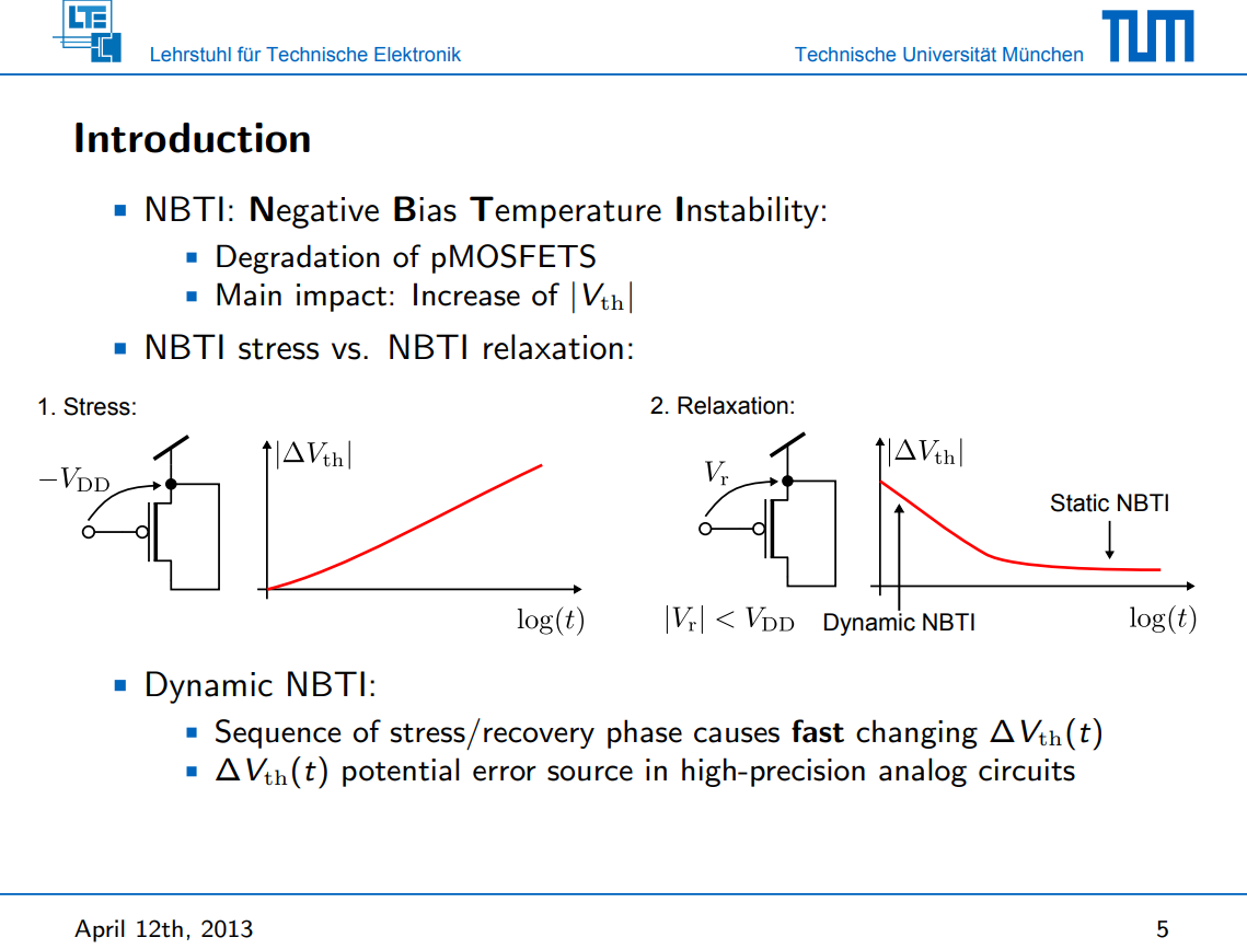
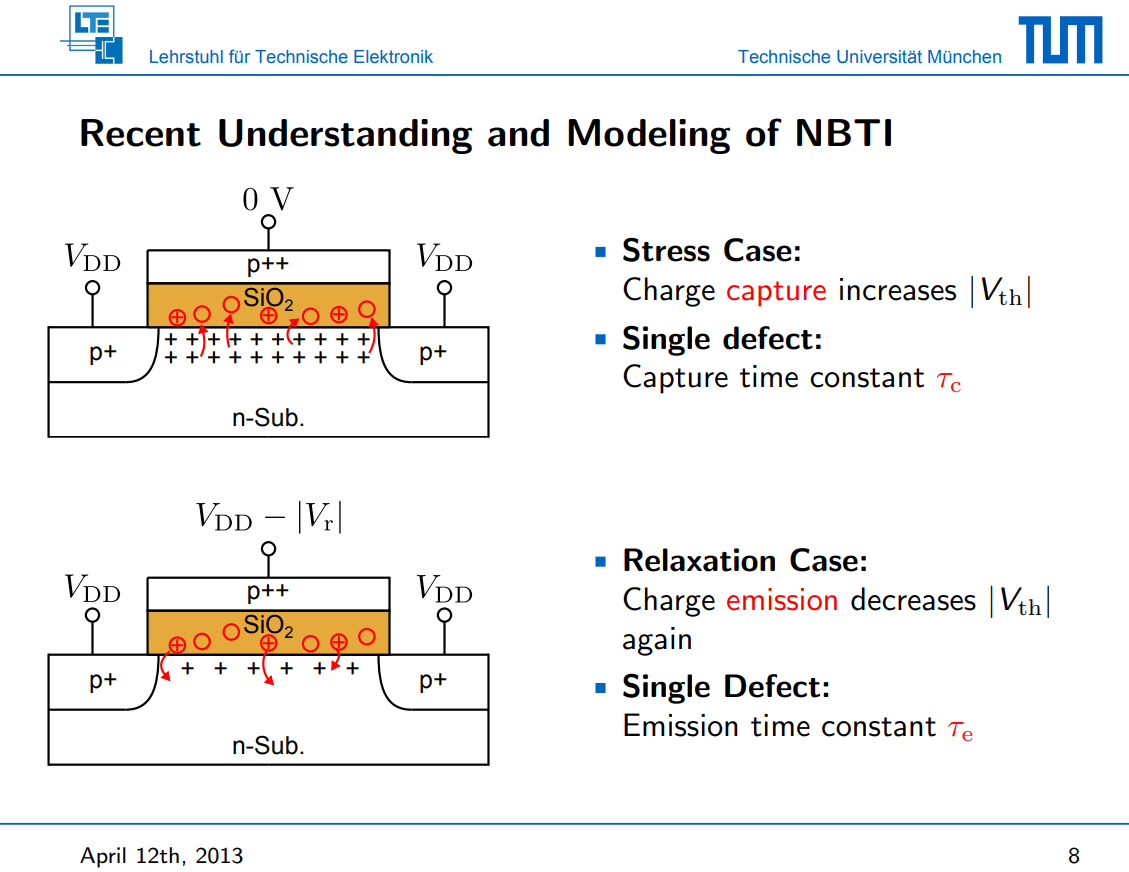
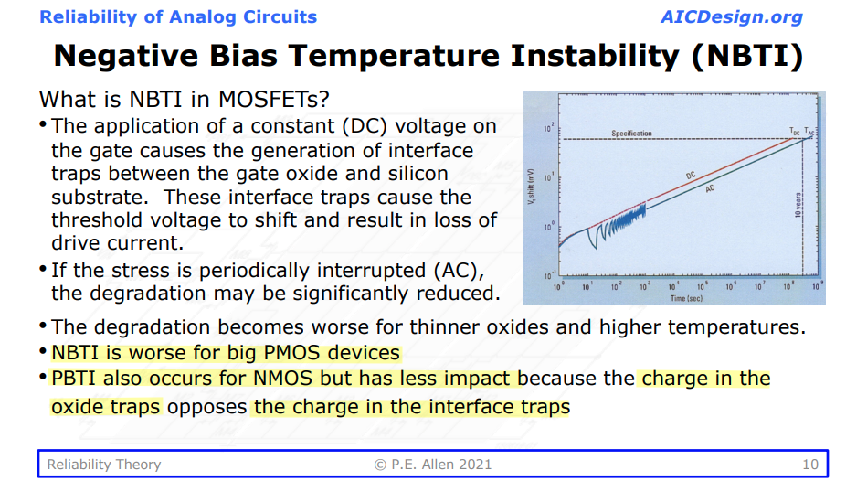
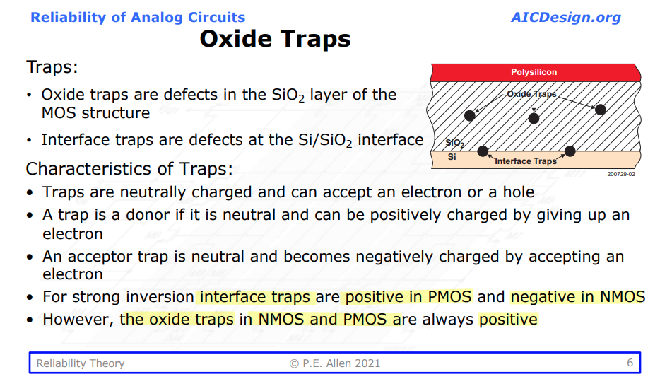
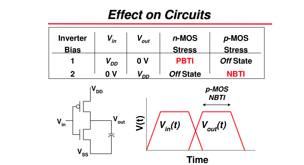
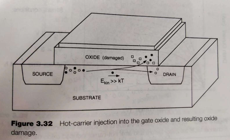
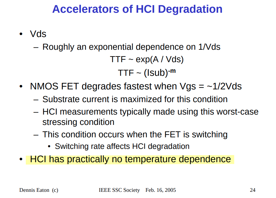 Unlike BTI, it seems to be no or just
little recovery. As holes are much "cooler" (i.e. heavier) than
electrons, the channel hot carrier effect in nMOS devices is shown to be
more significant than in pMOS devices.
Unlike BTI, it seems to be no or just
little recovery. As holes are much "cooler" (i.e. heavier) than
electrons, the channel hot carrier effect in nMOS devices is shown to be
more significant than in pMOS devices.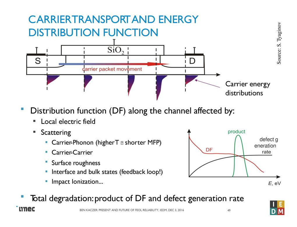
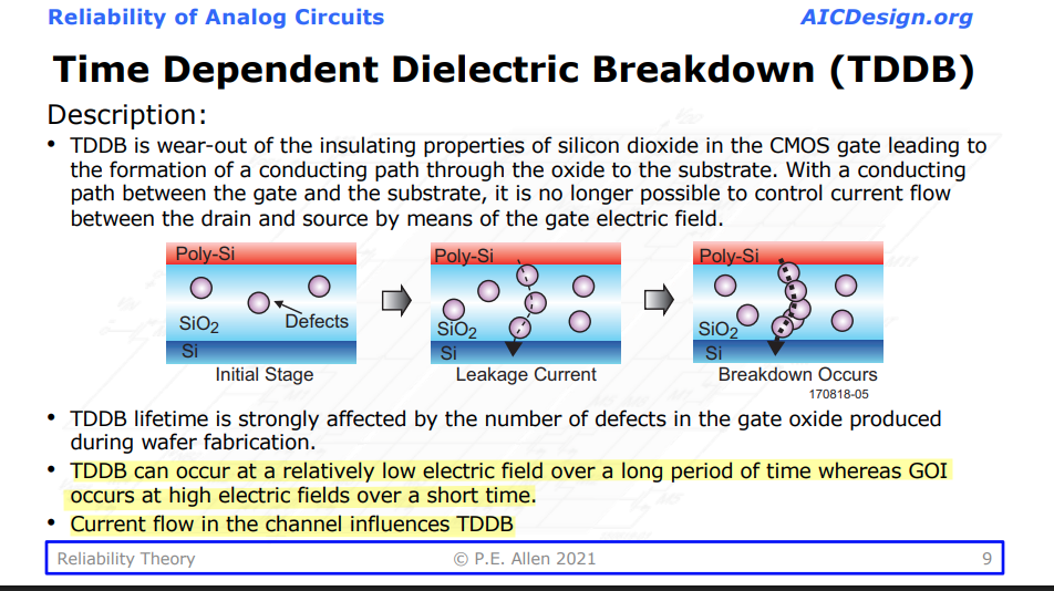
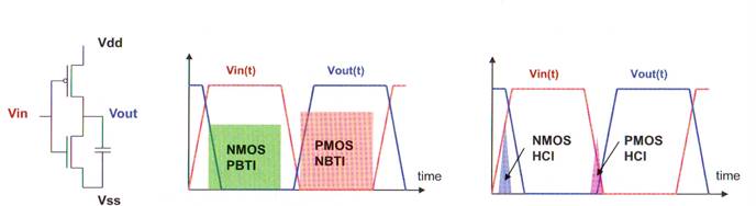
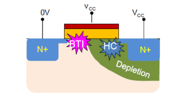
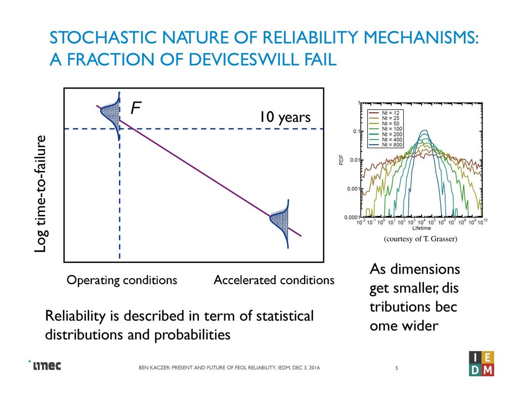
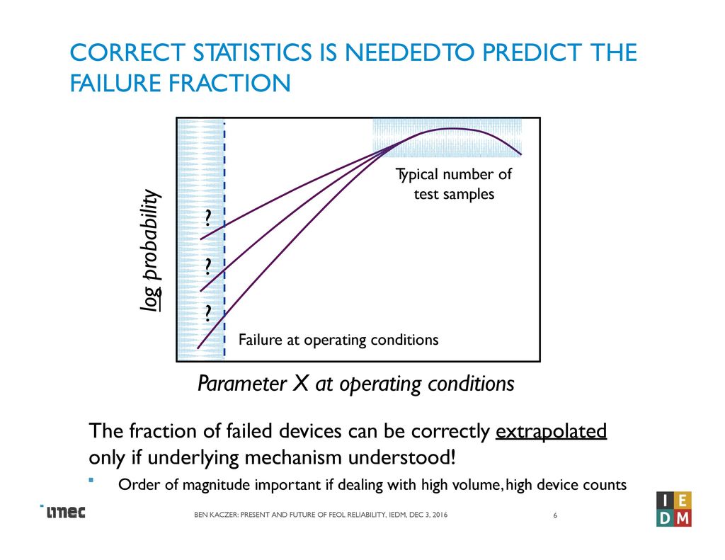
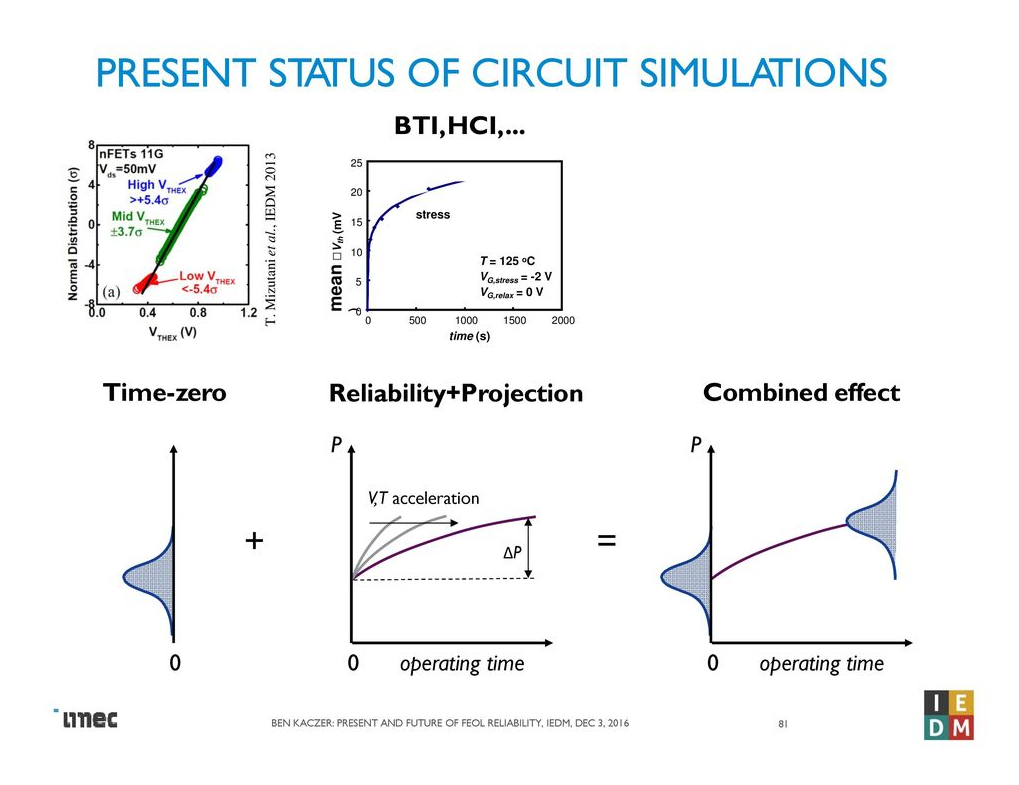
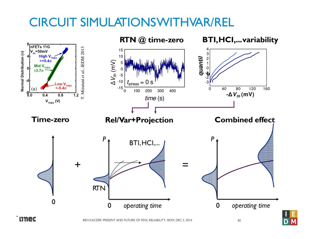
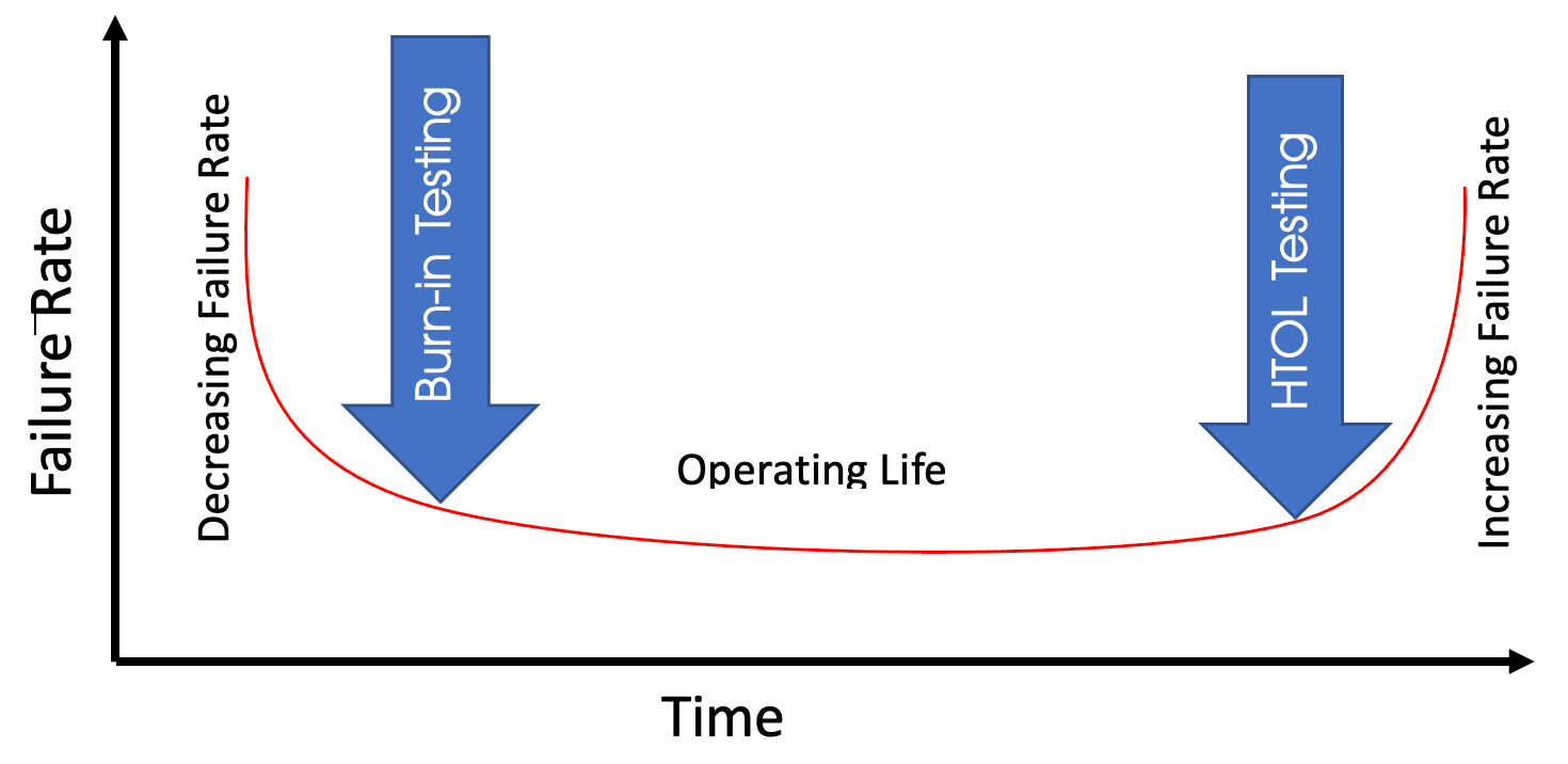
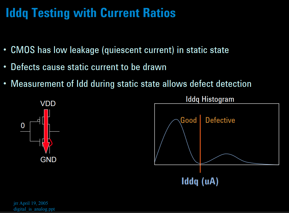
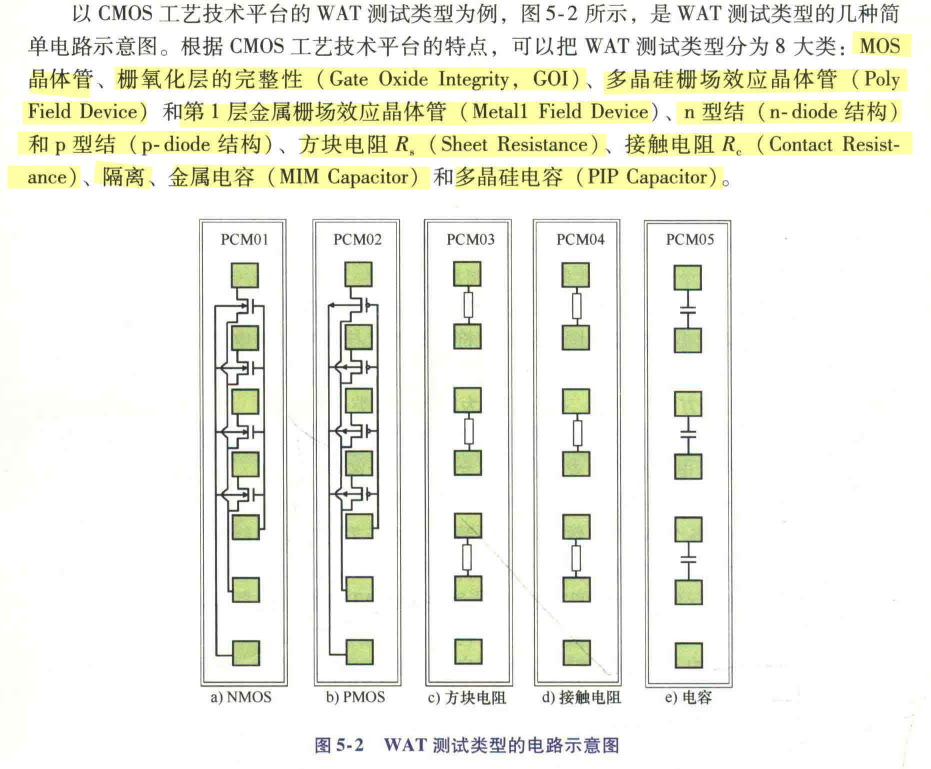
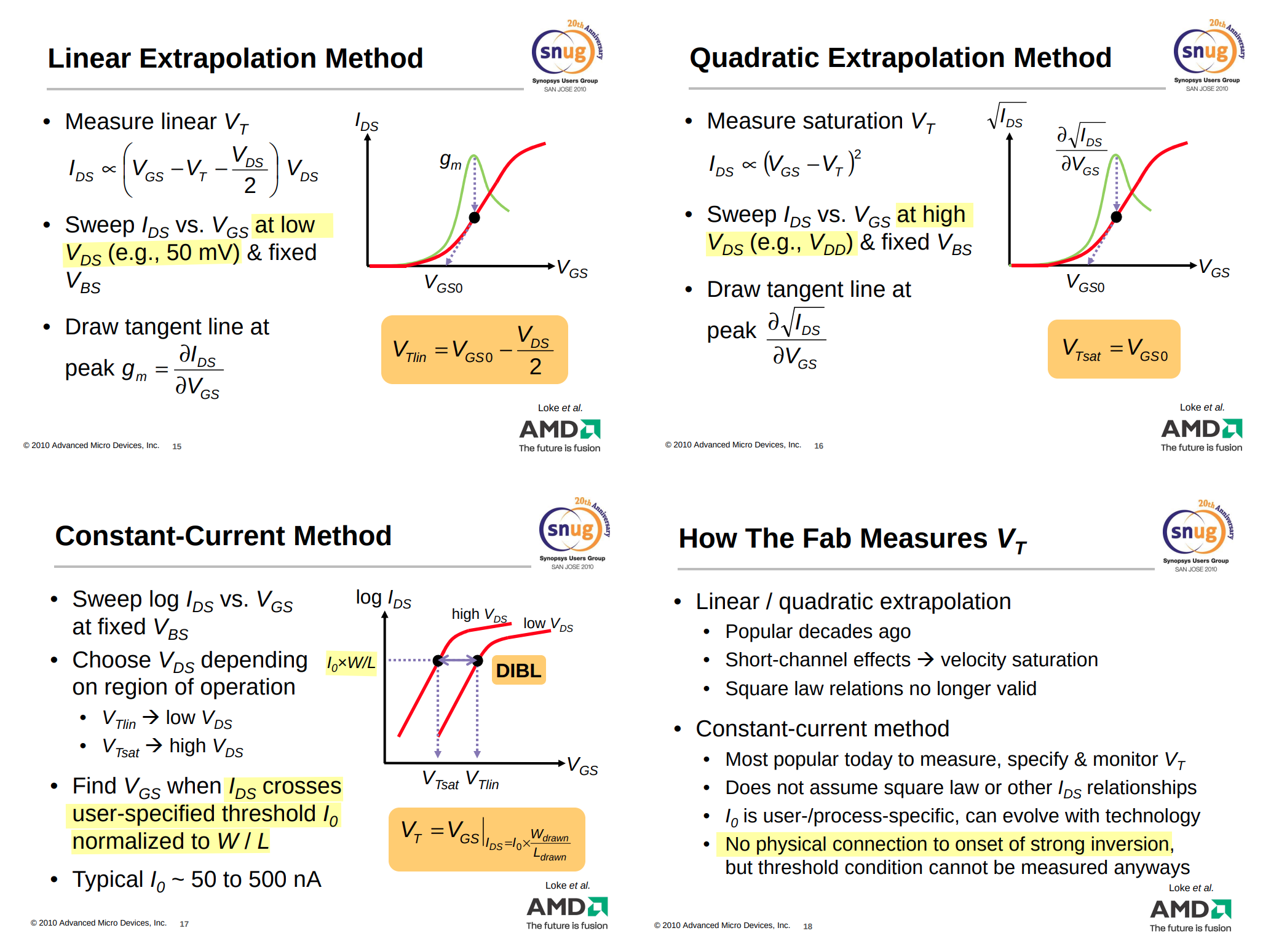
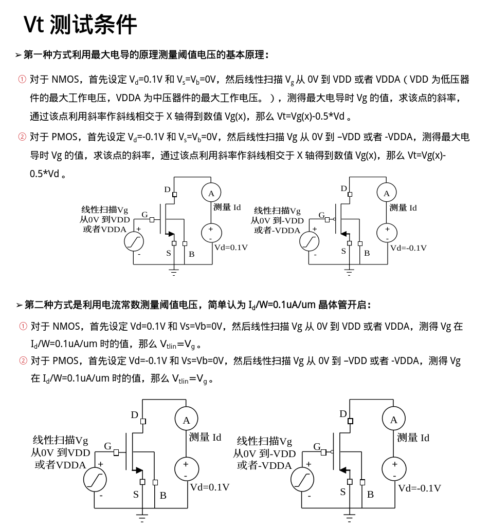

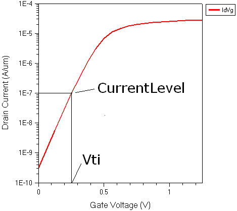
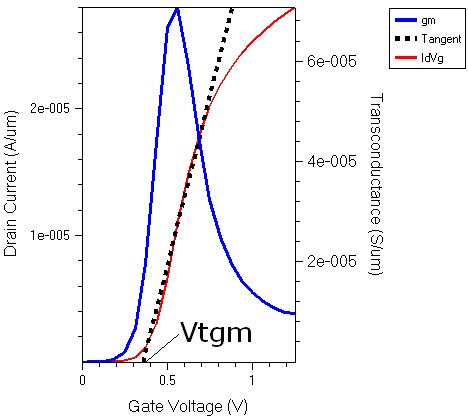
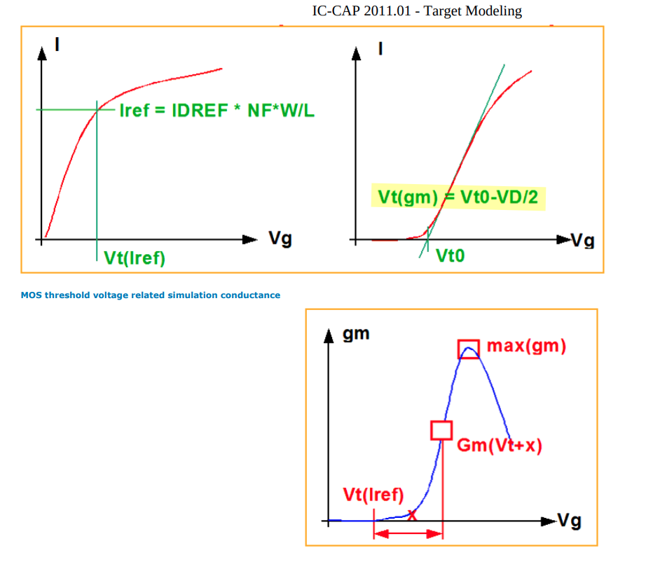
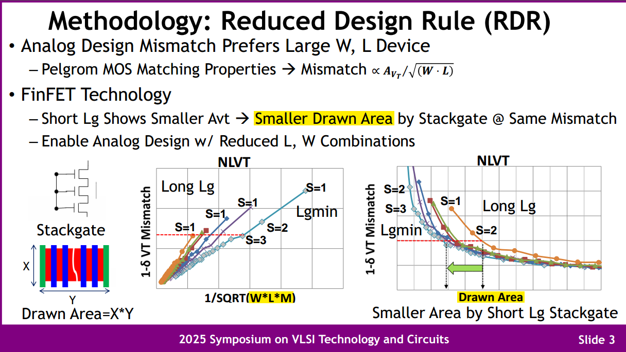
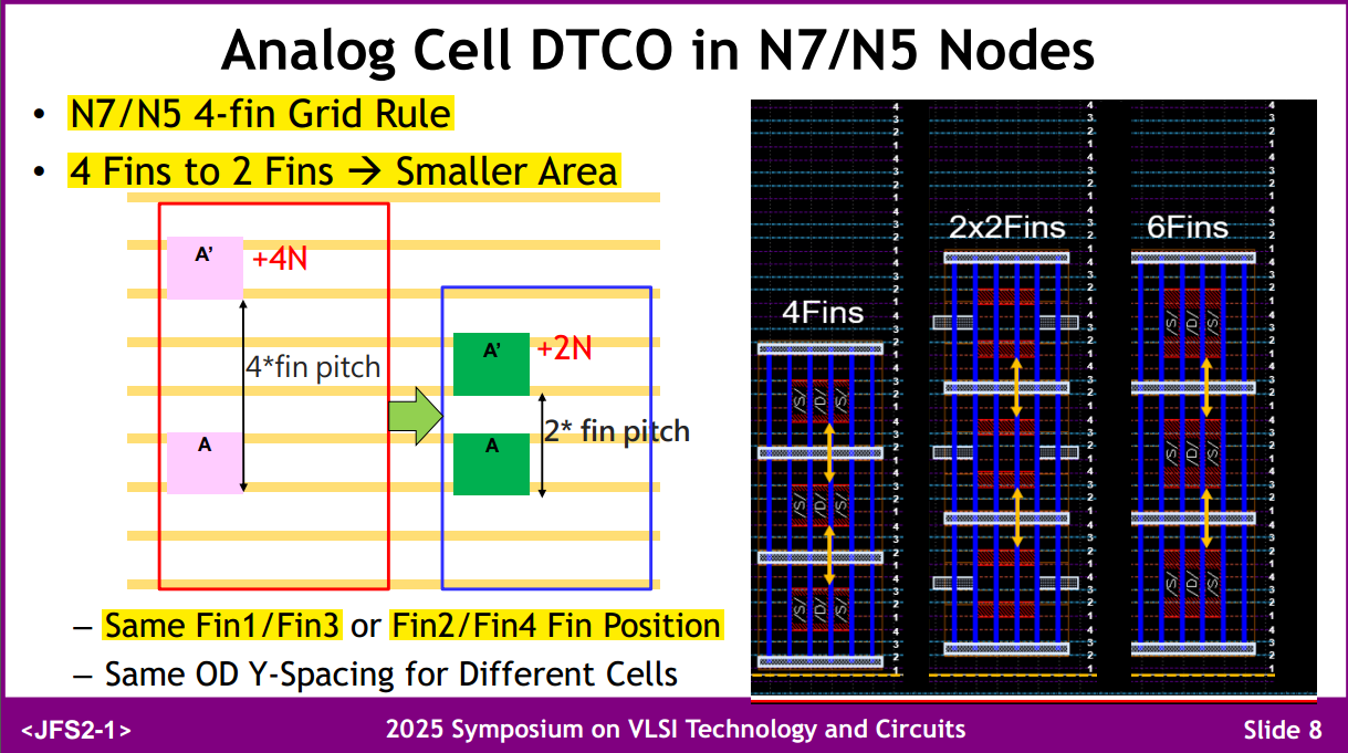
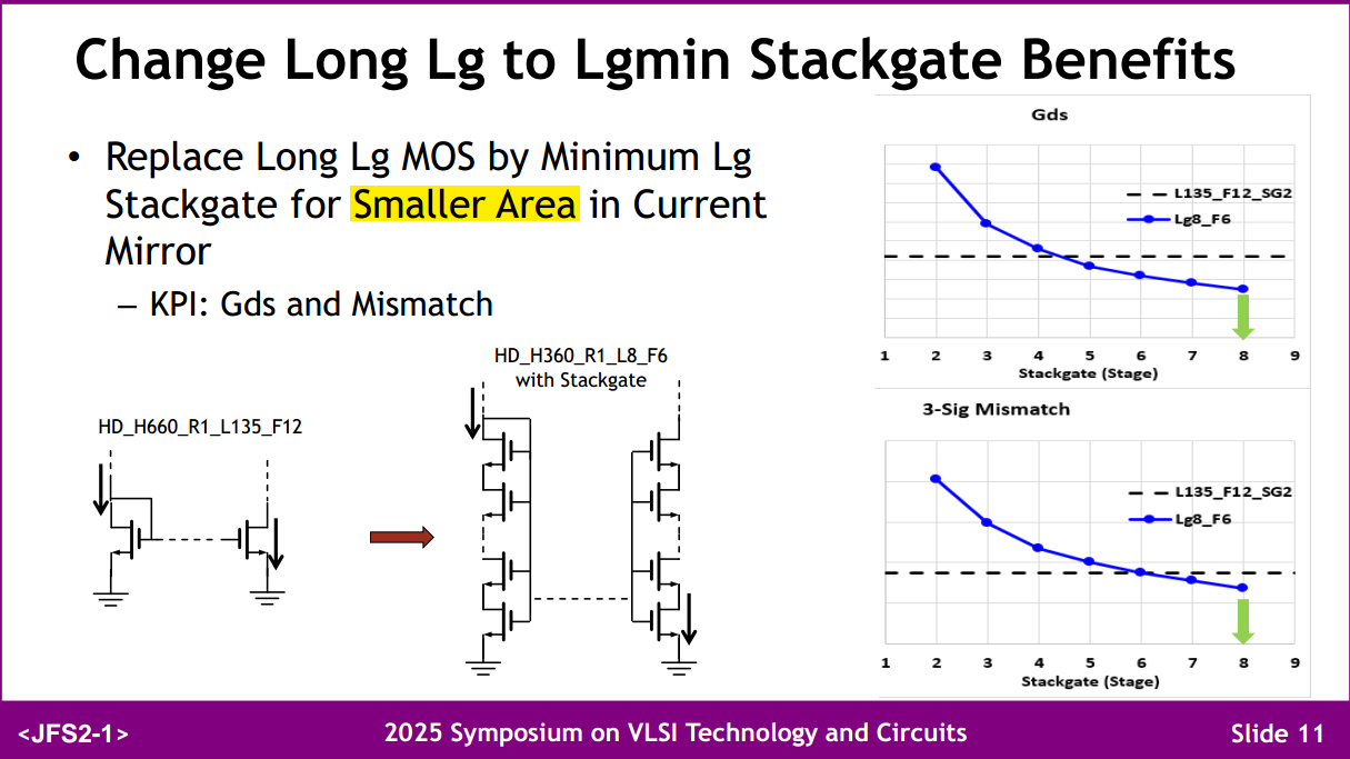
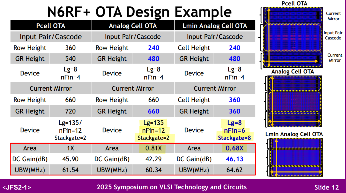
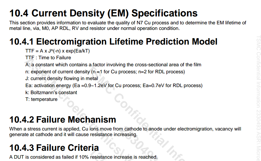
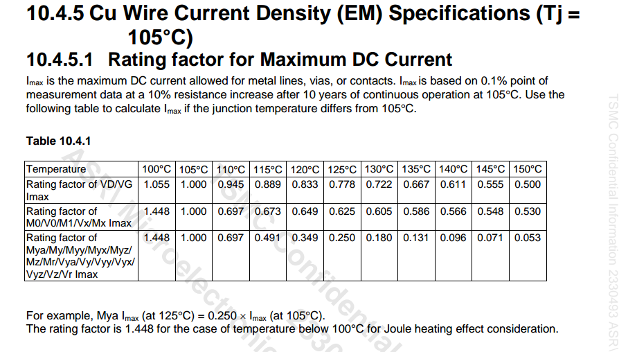
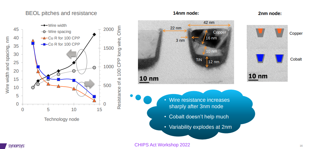


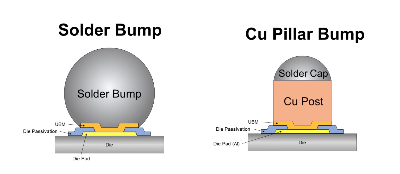
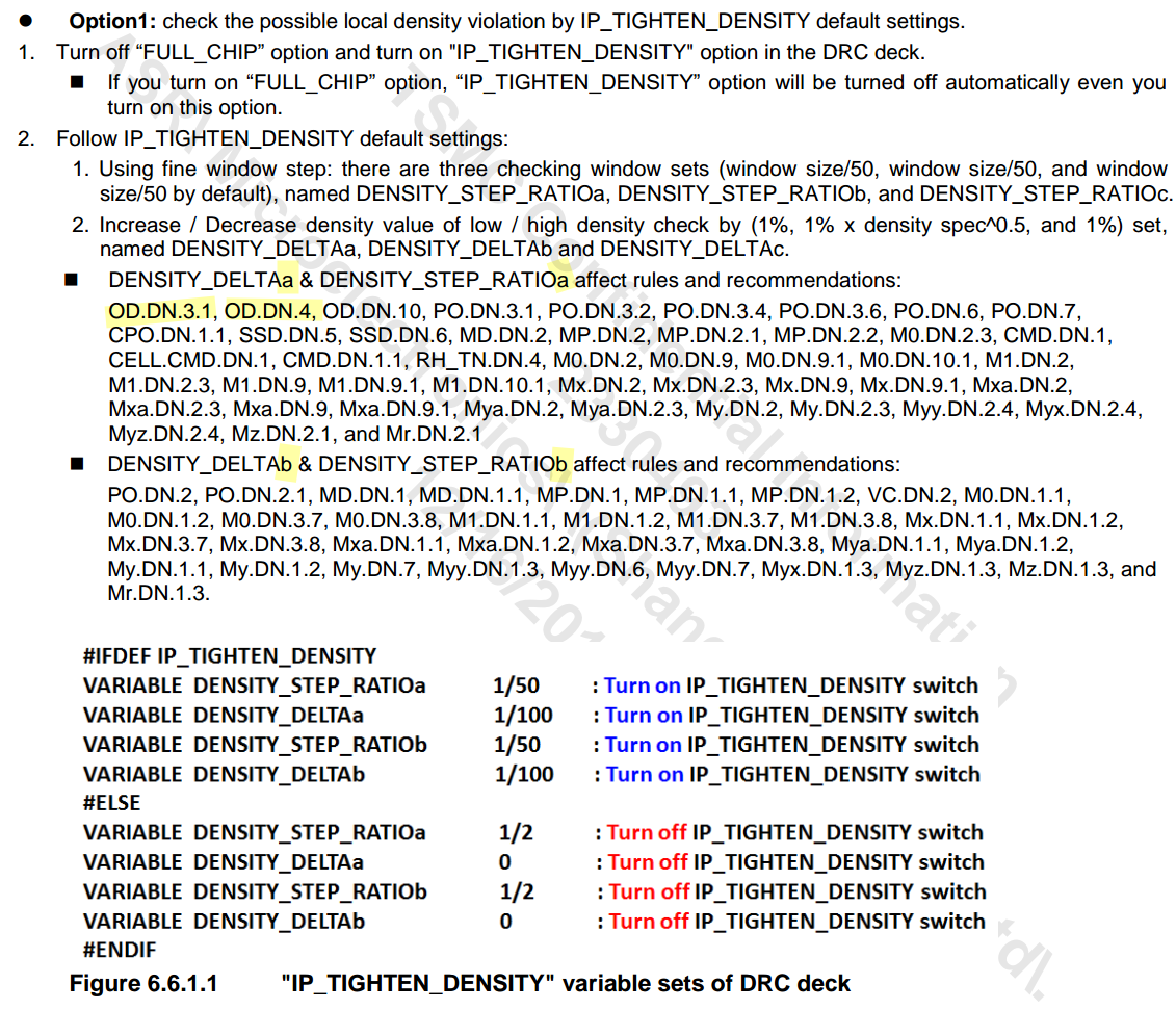
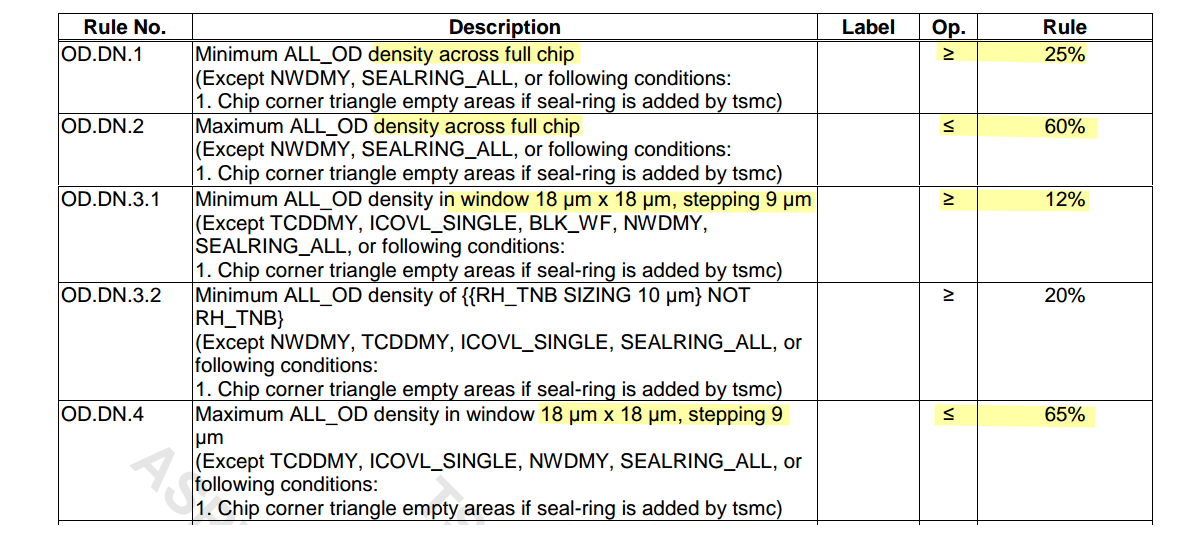
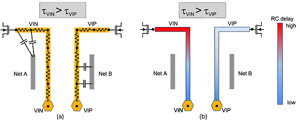
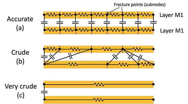
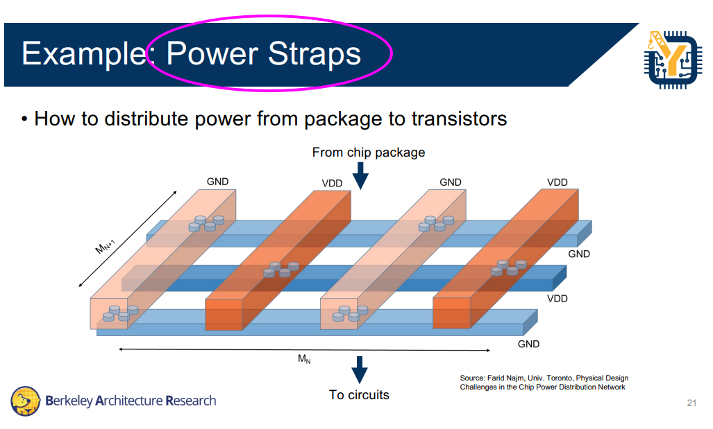
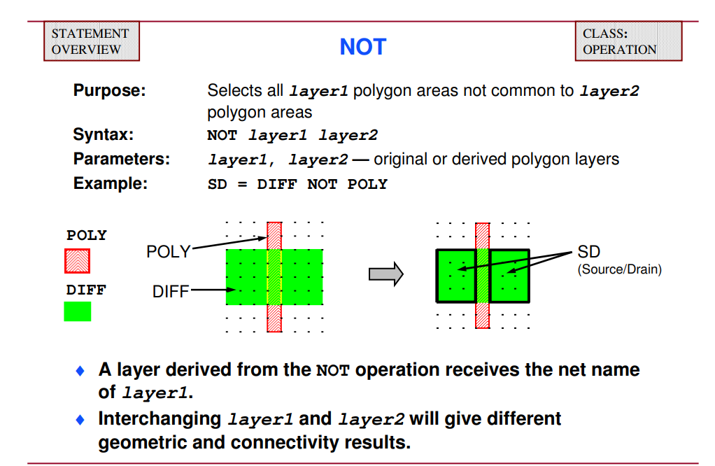
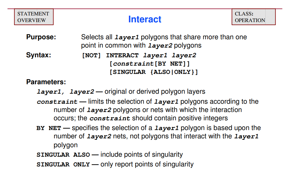
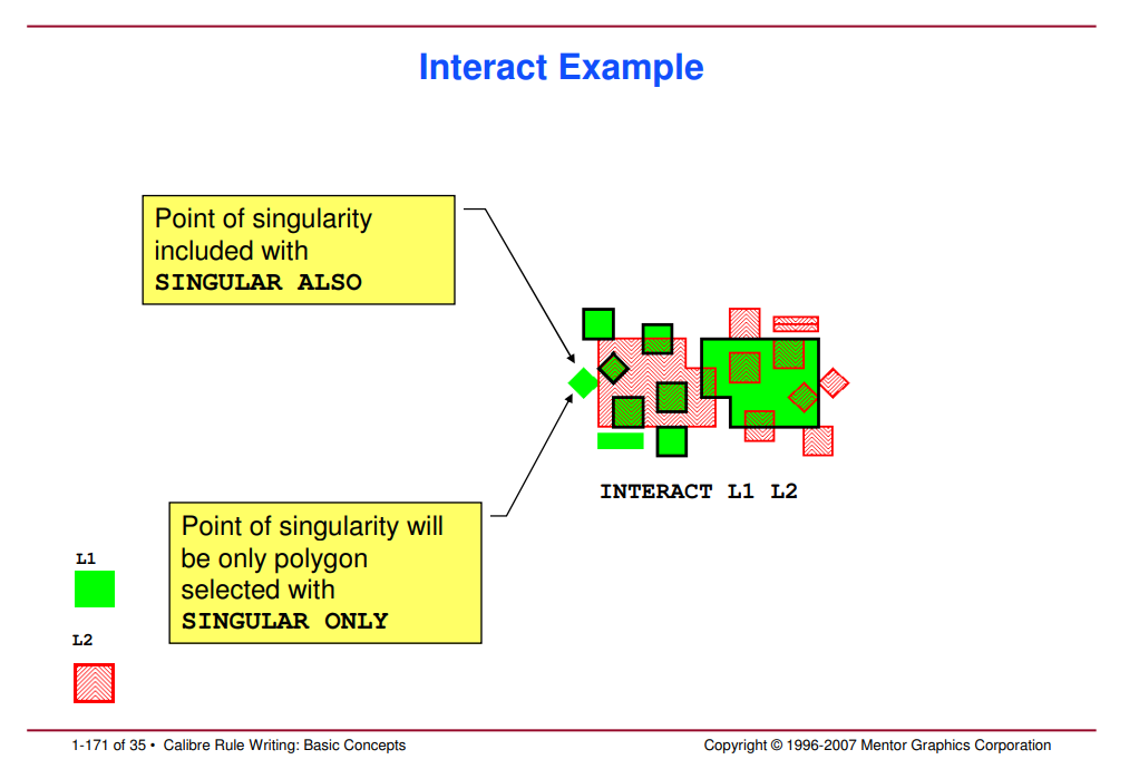
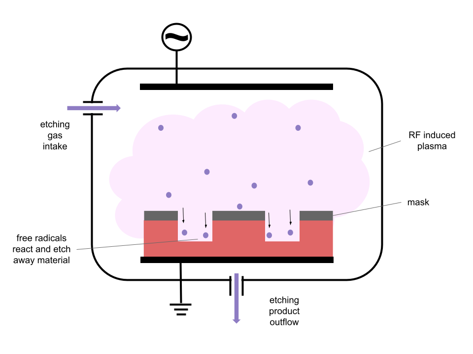
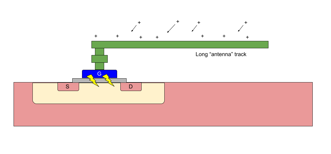
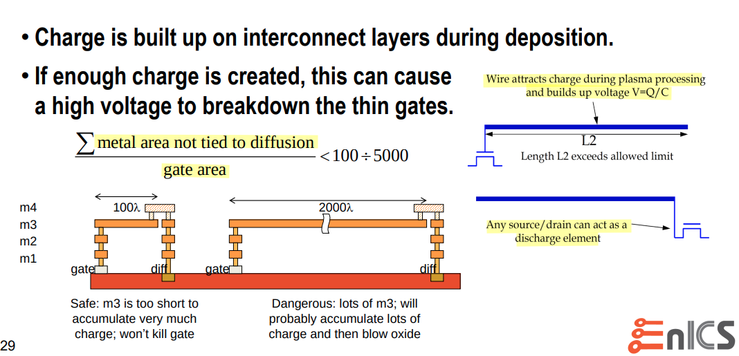
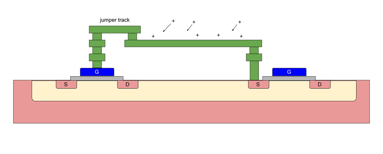
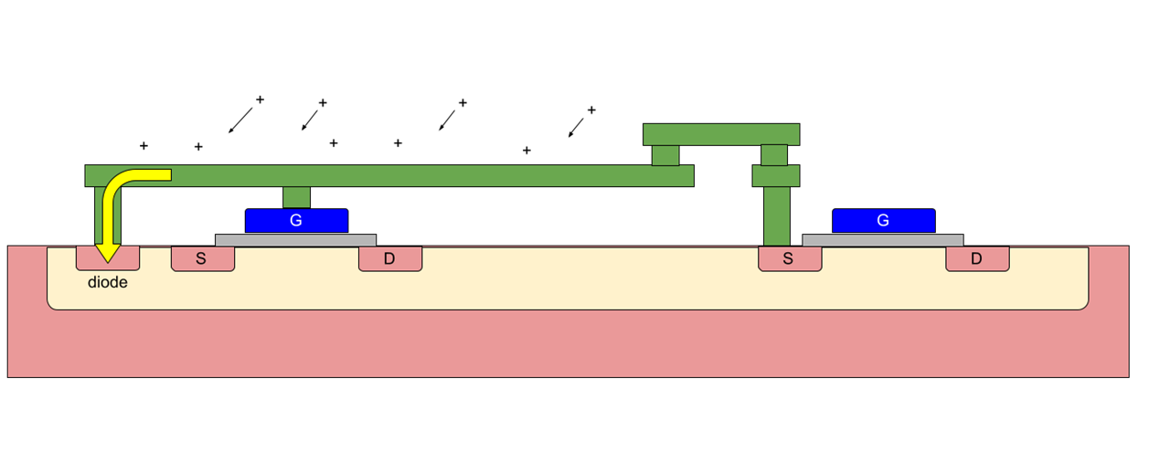
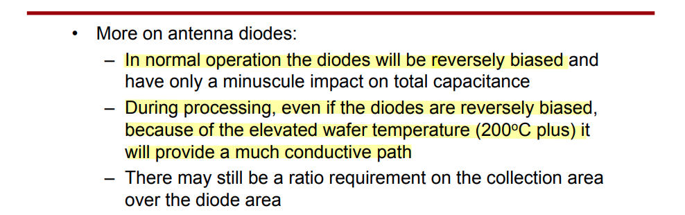
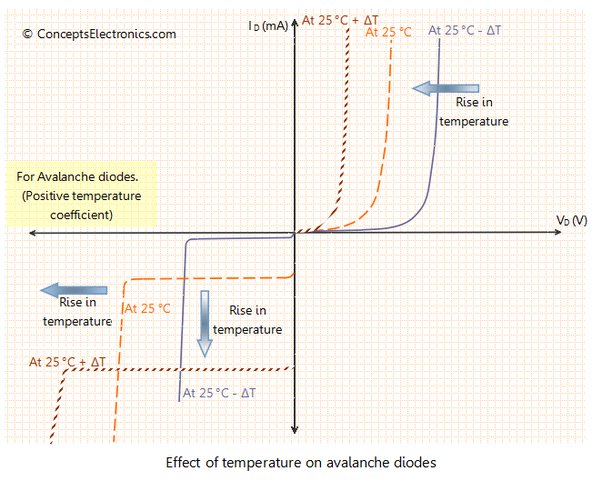
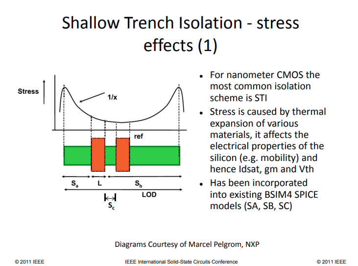
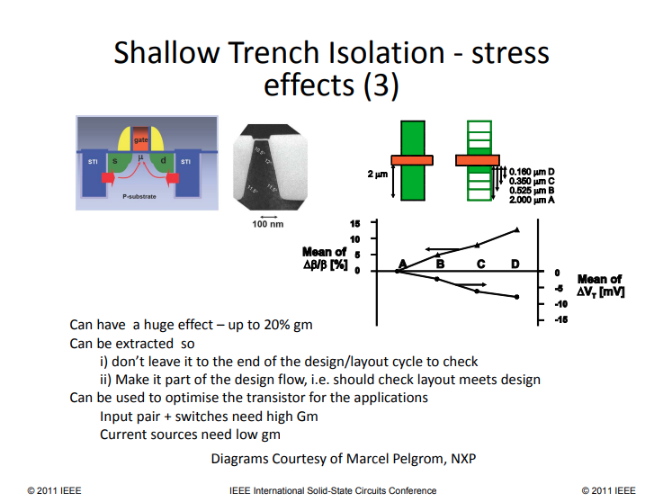
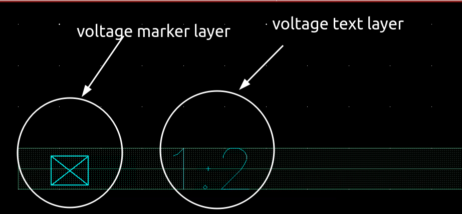


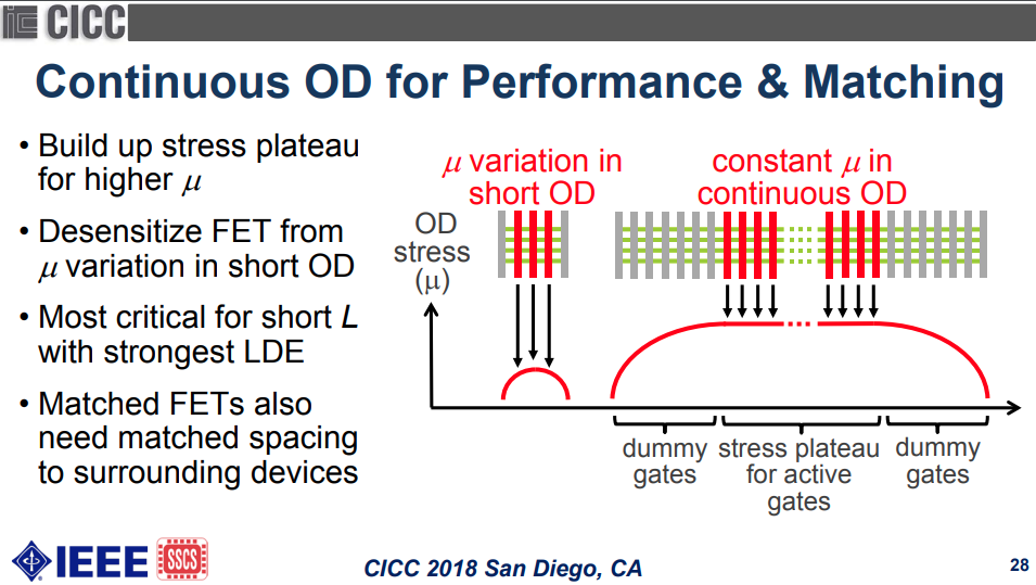


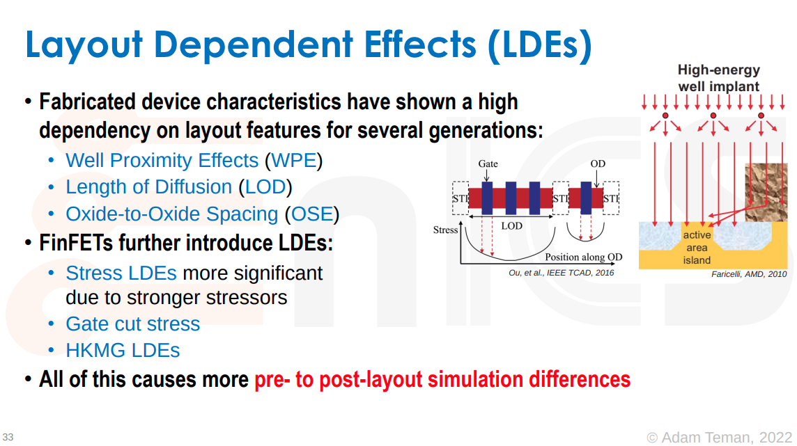
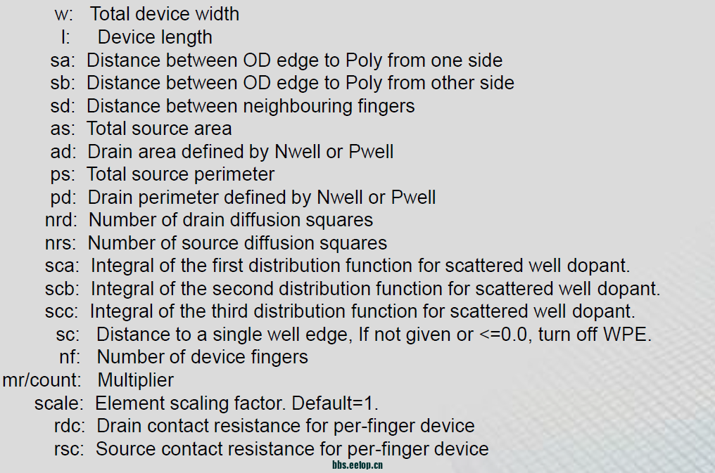
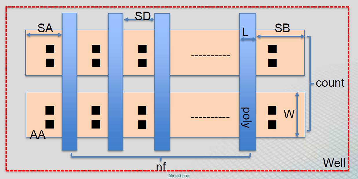
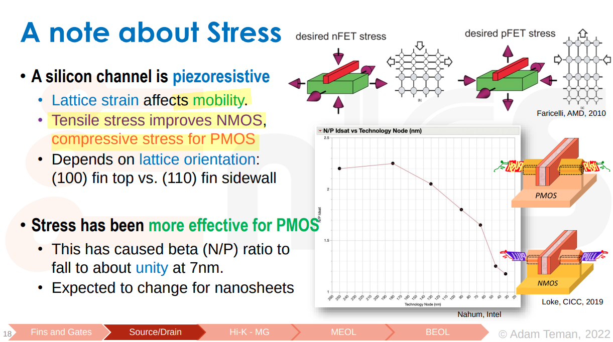
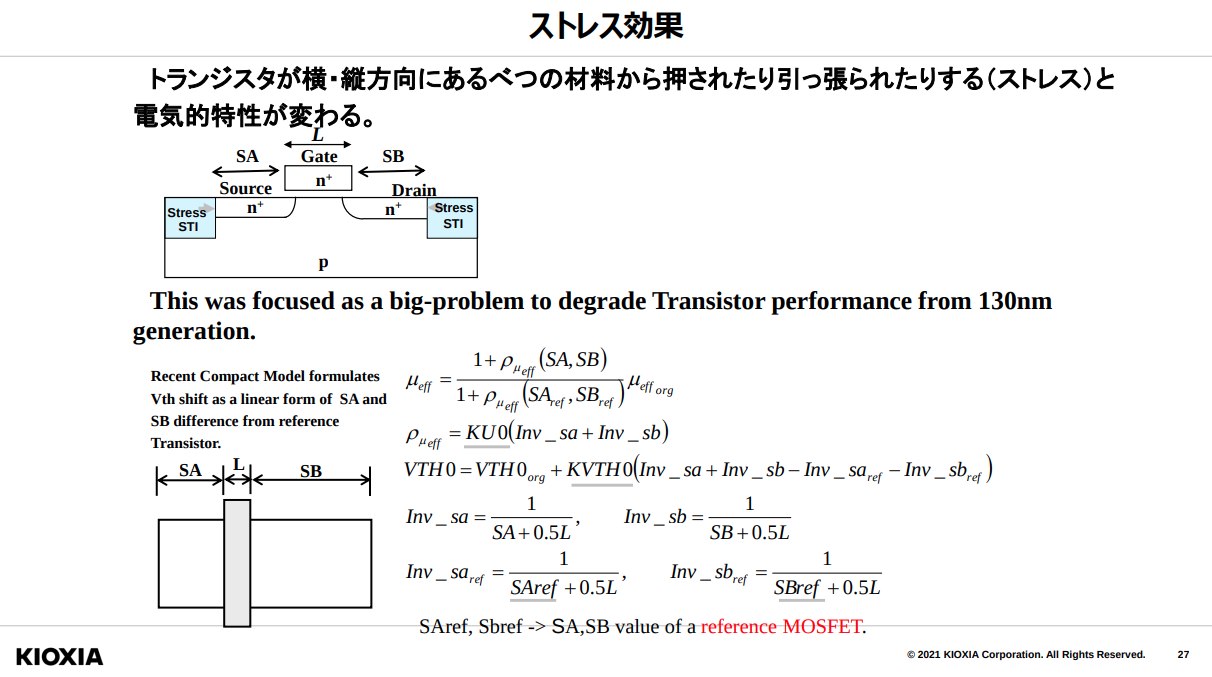
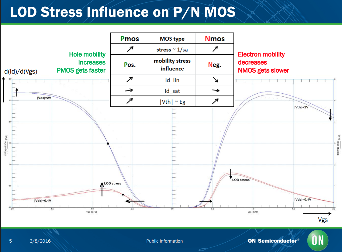
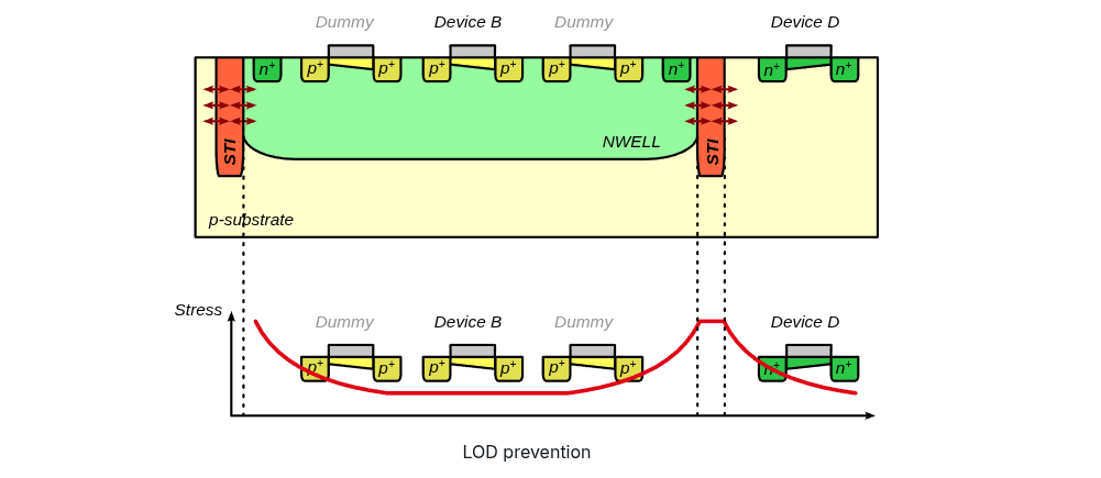
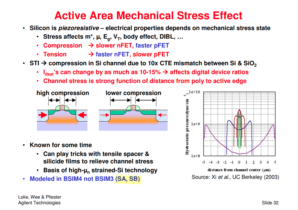
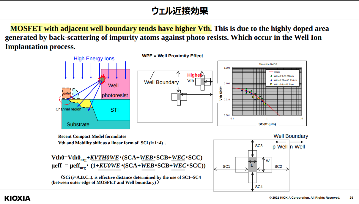
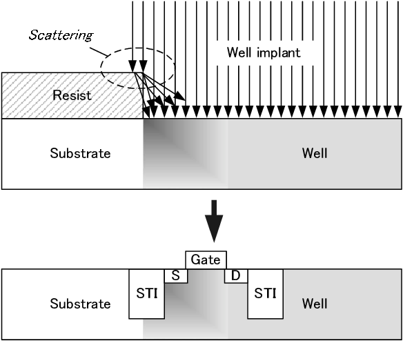
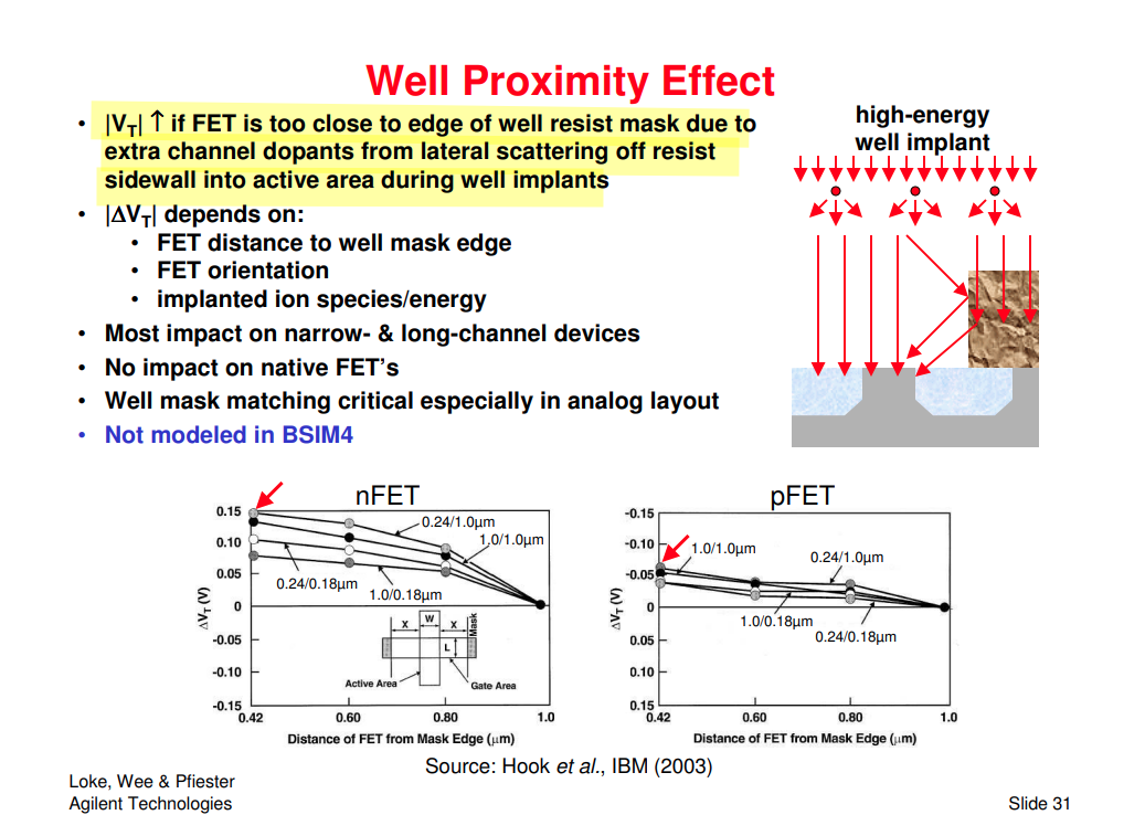
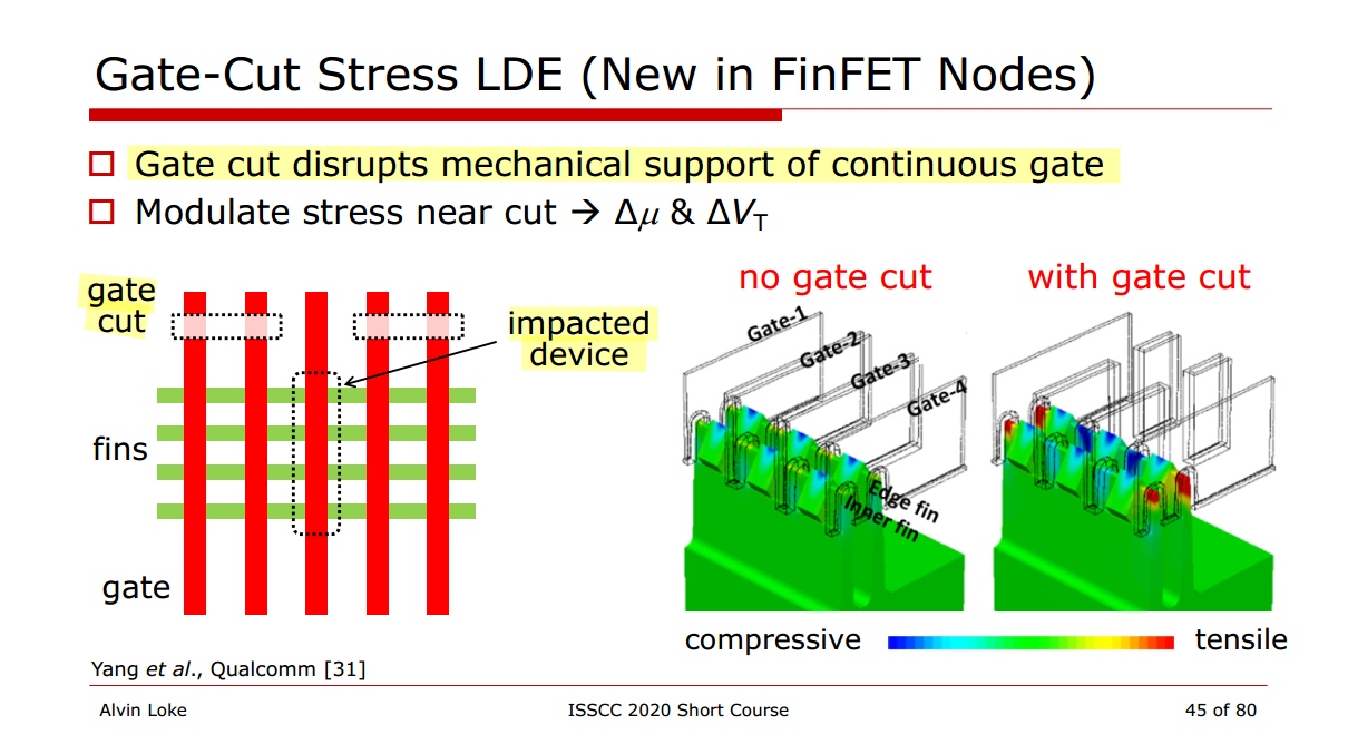

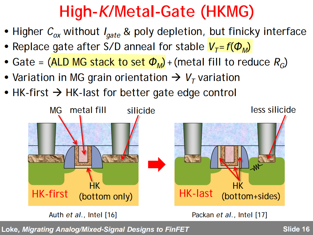
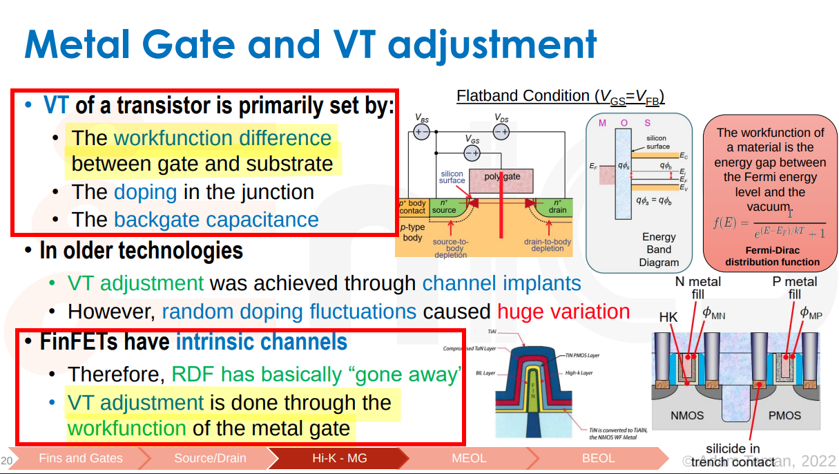
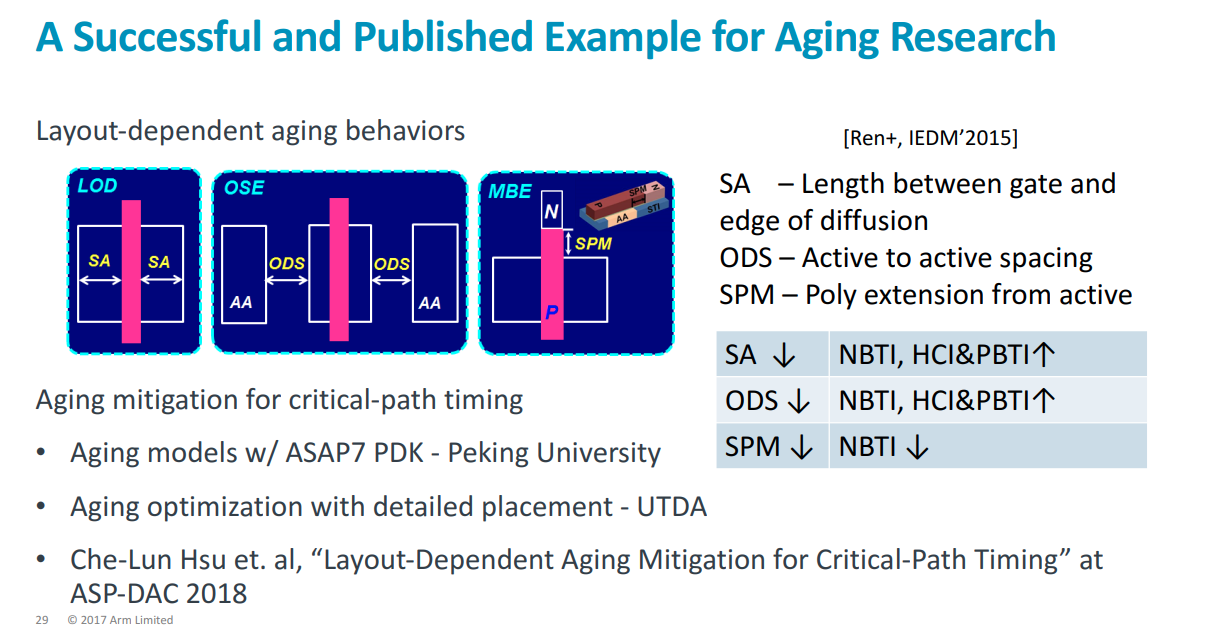
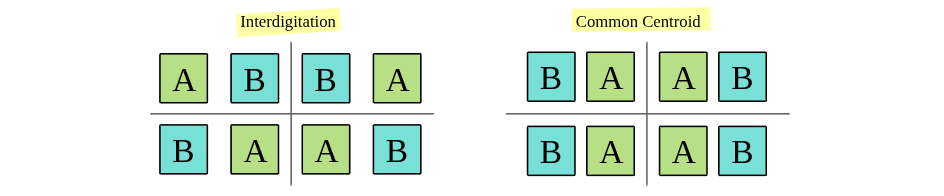

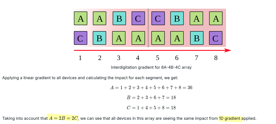
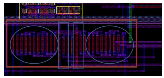
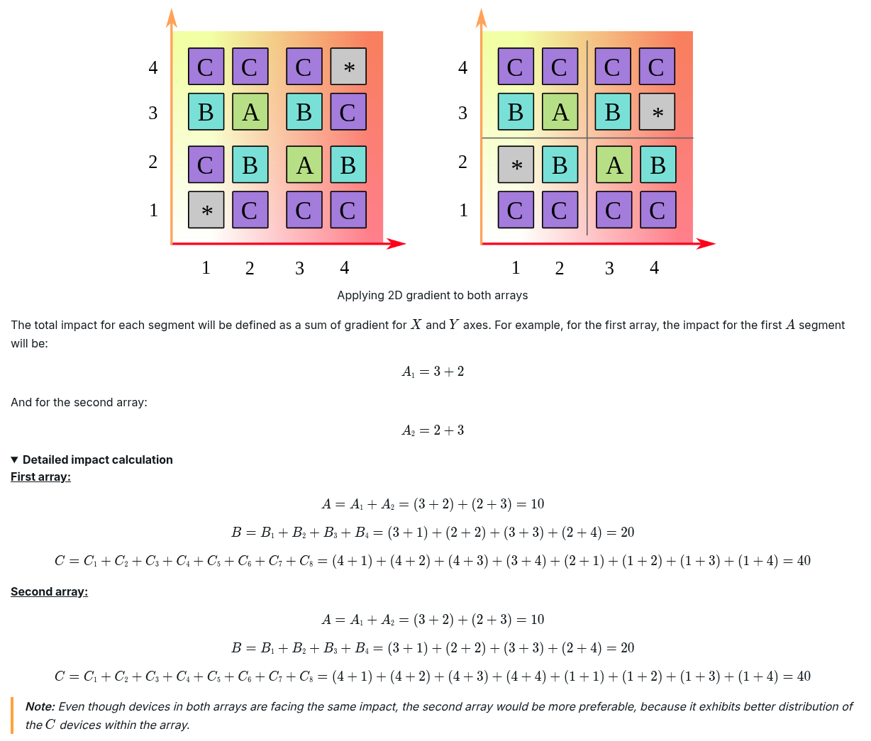
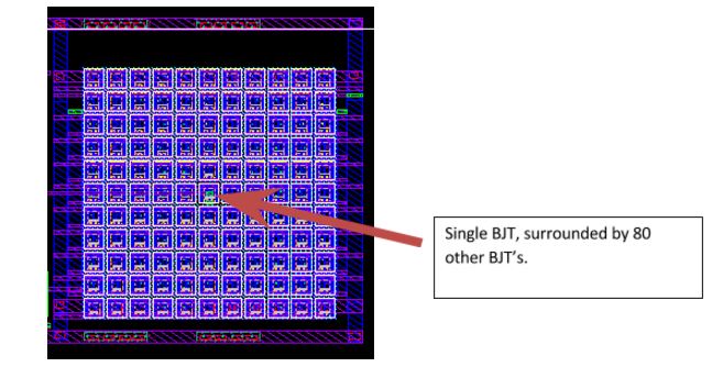
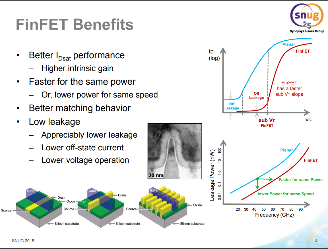
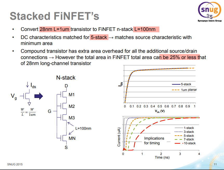
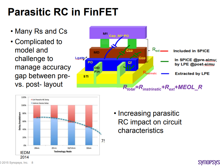
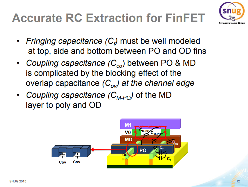

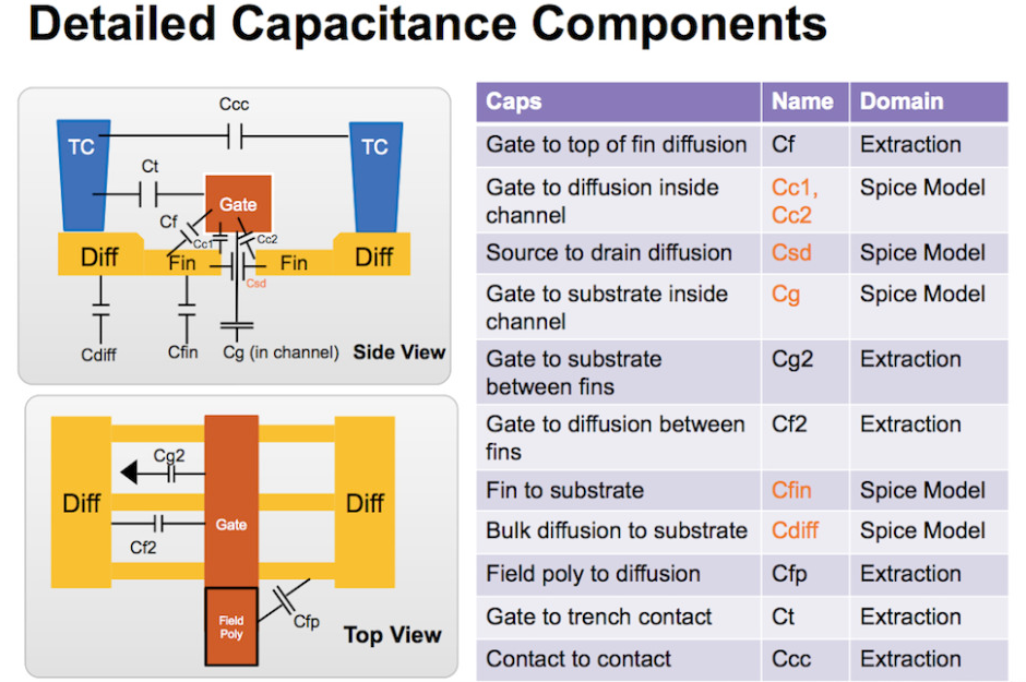
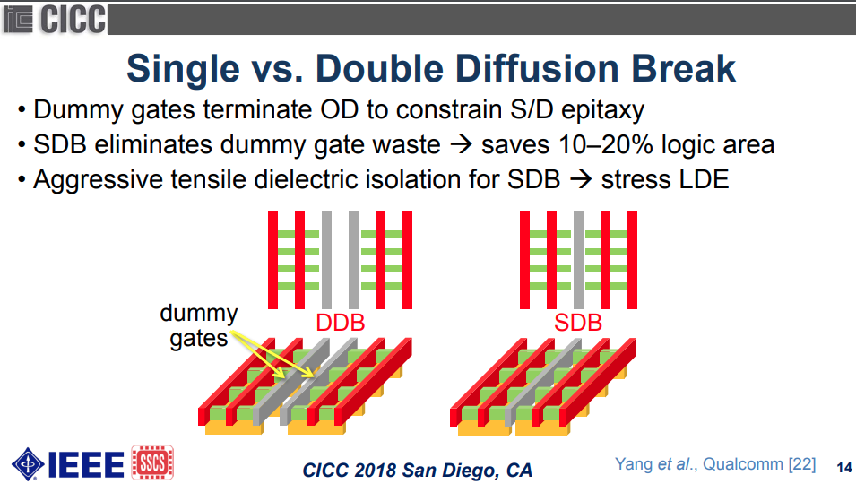
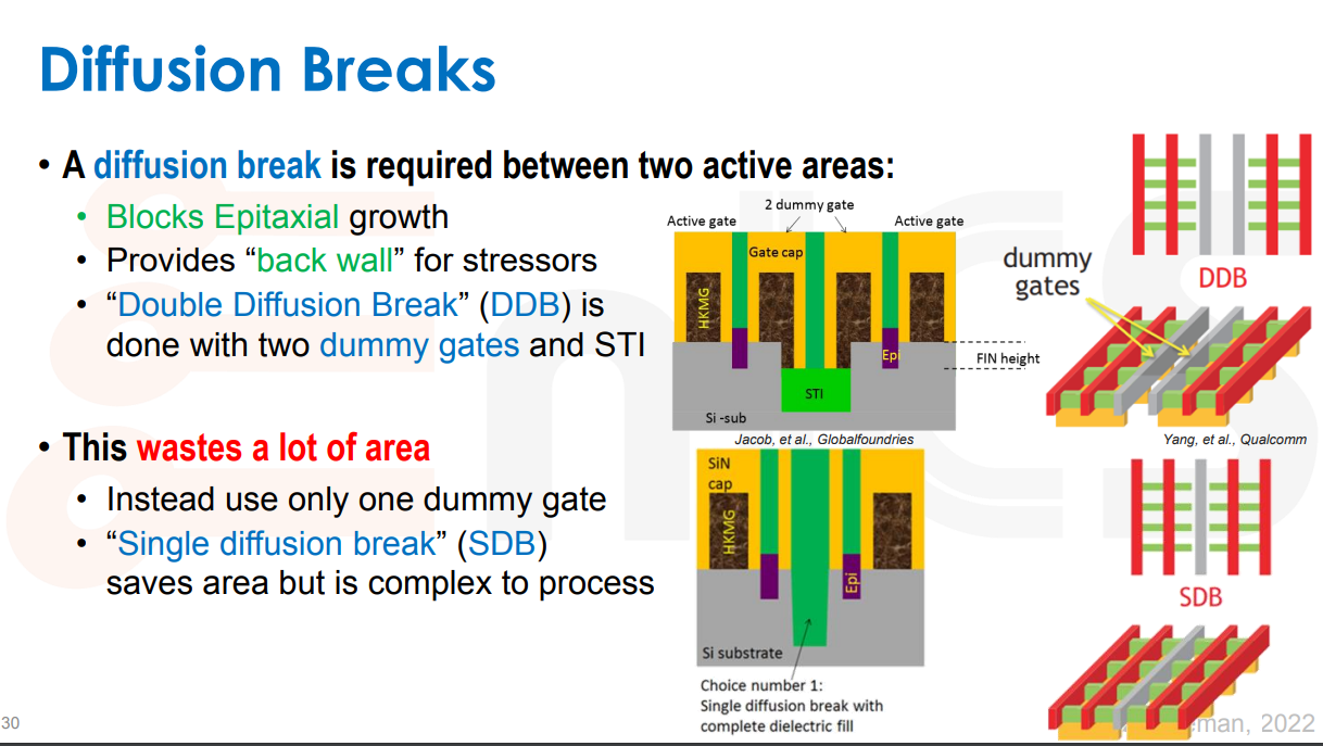
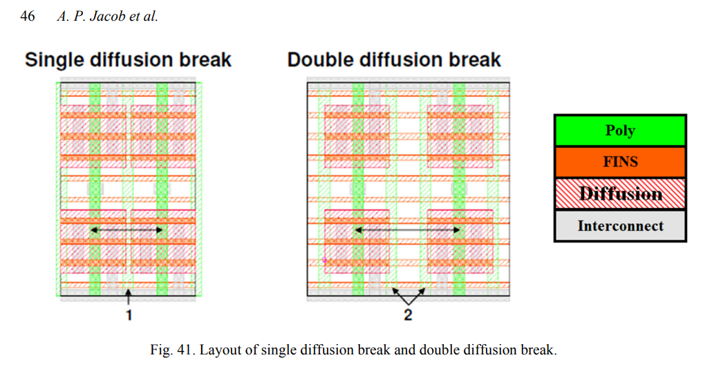
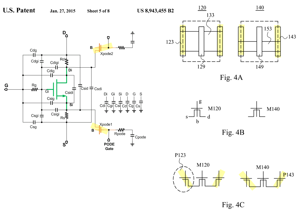
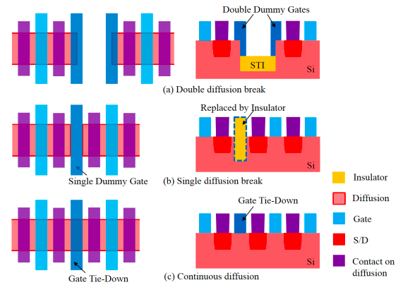
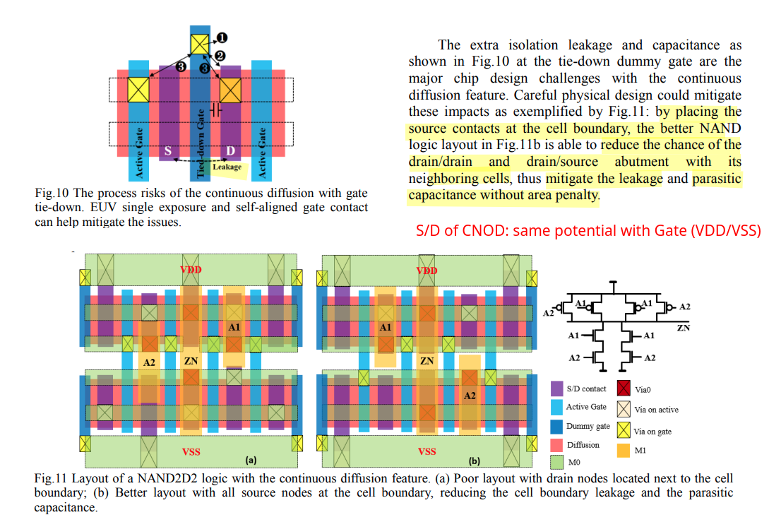
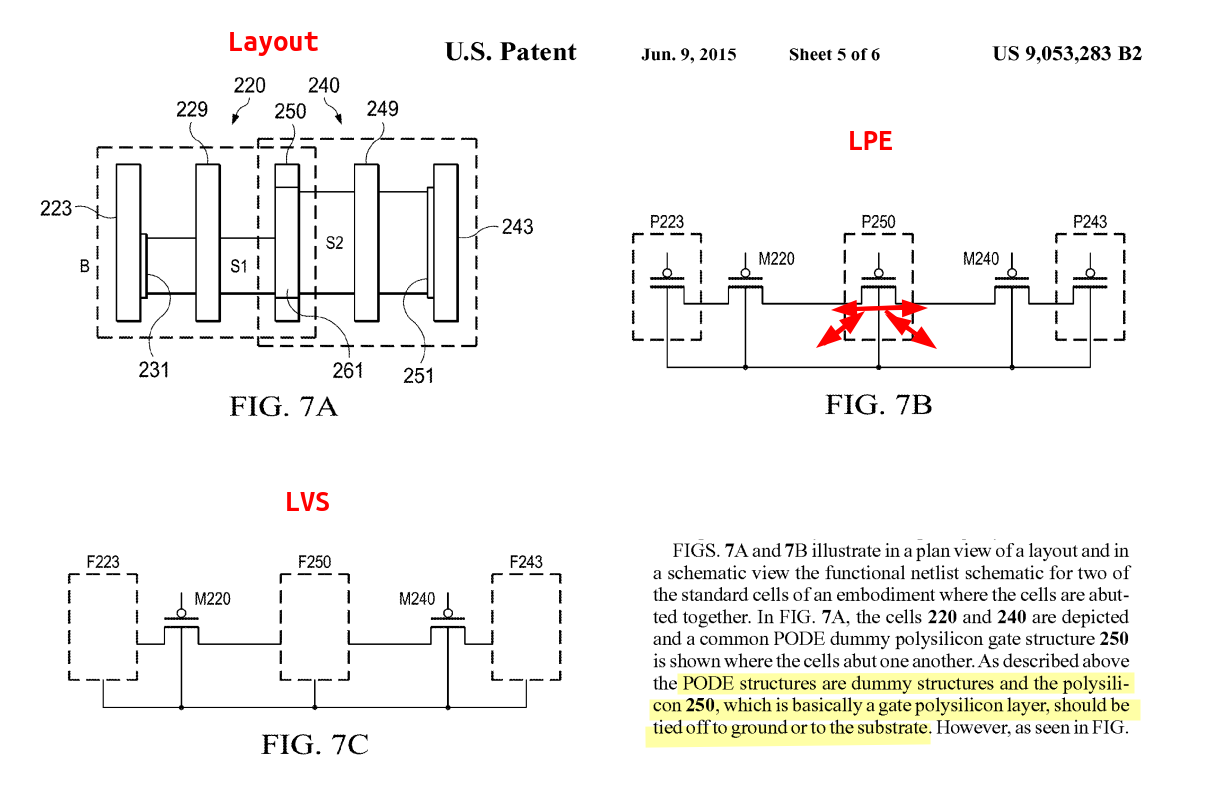
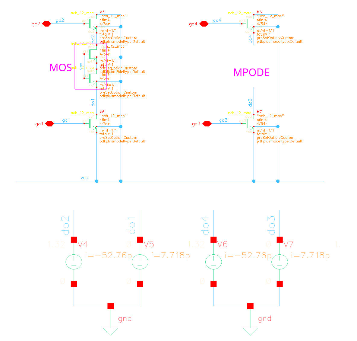
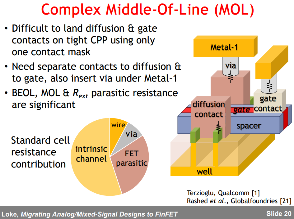
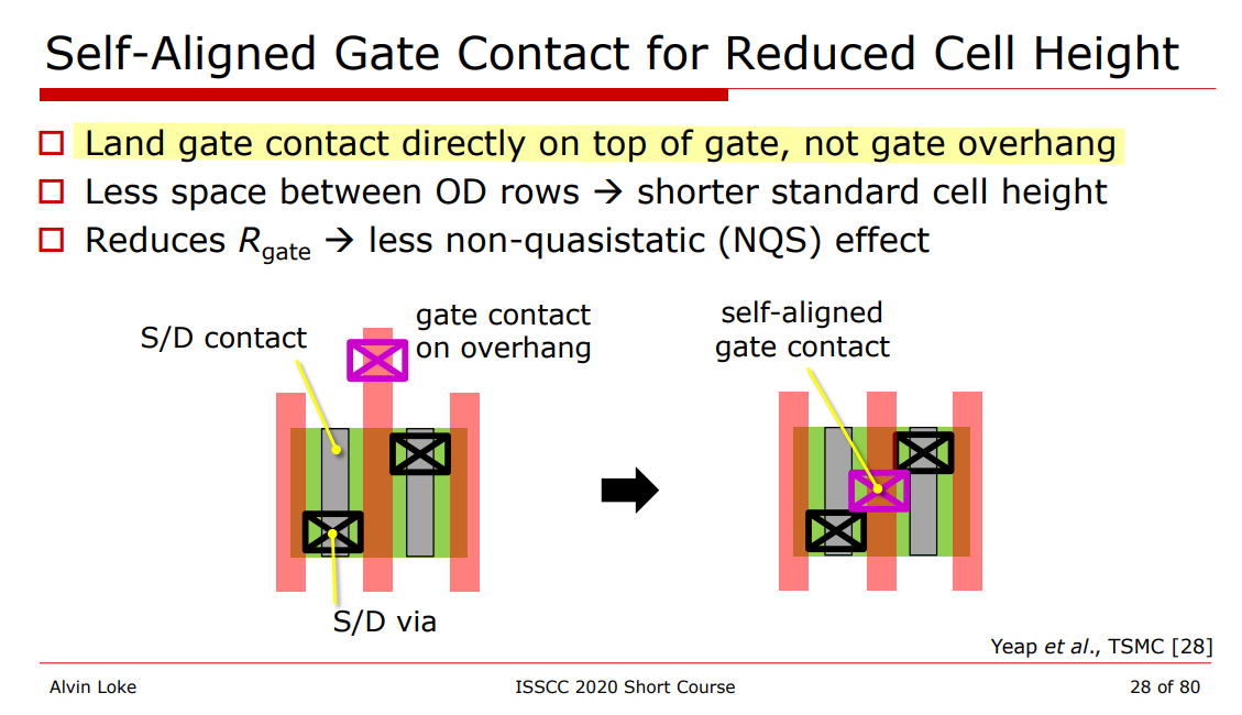
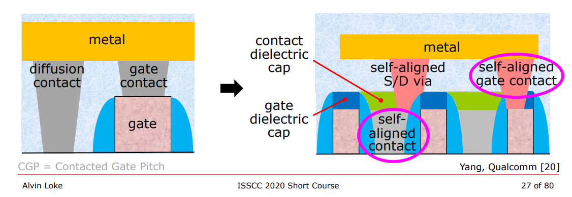
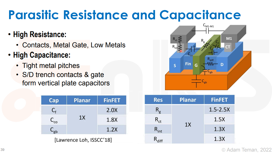
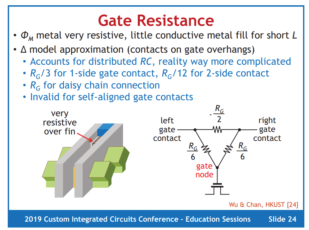
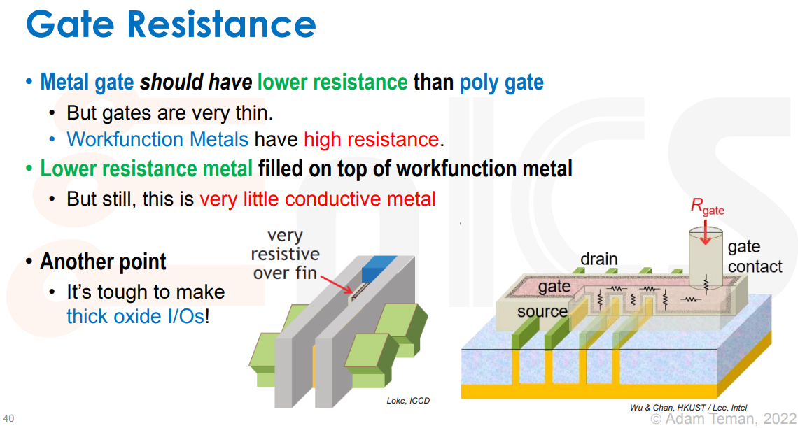
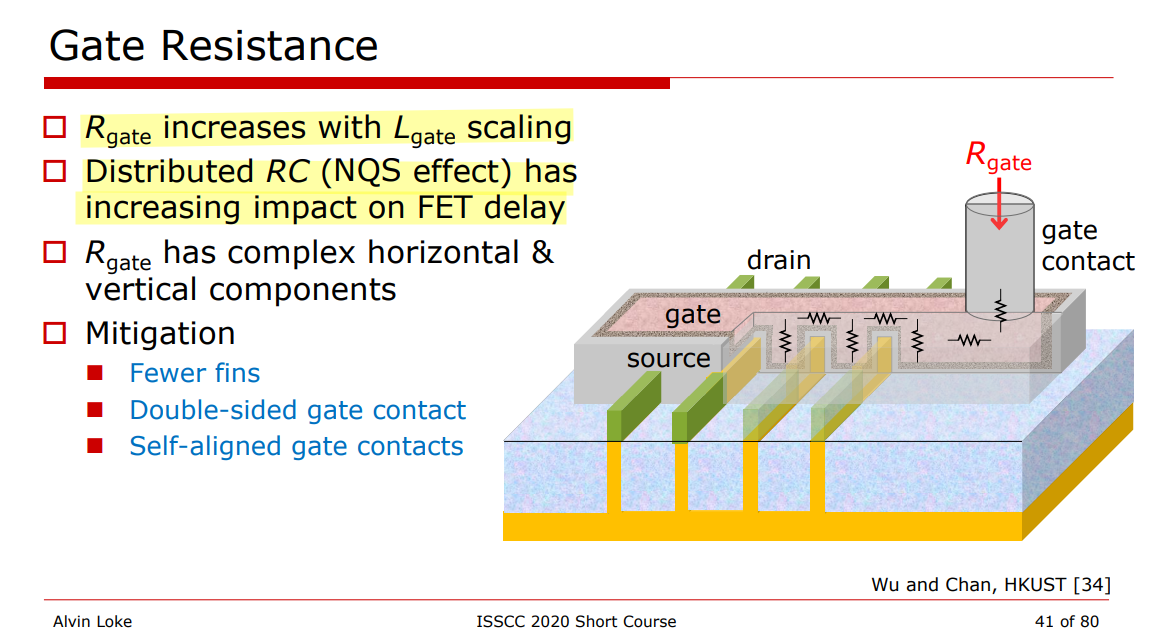
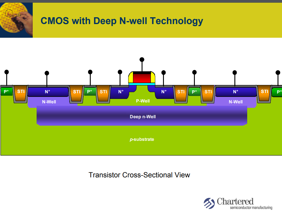
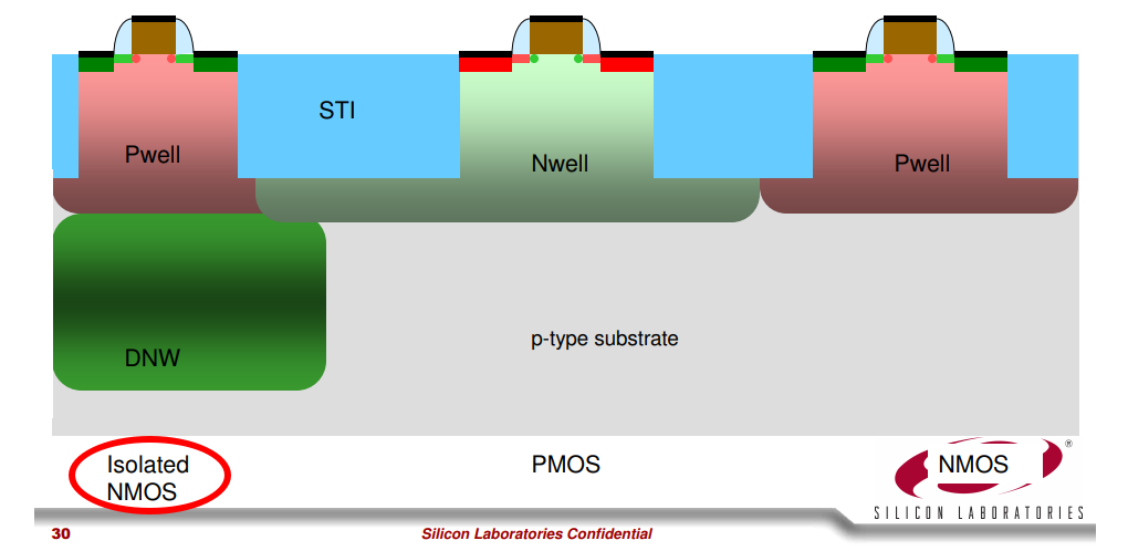
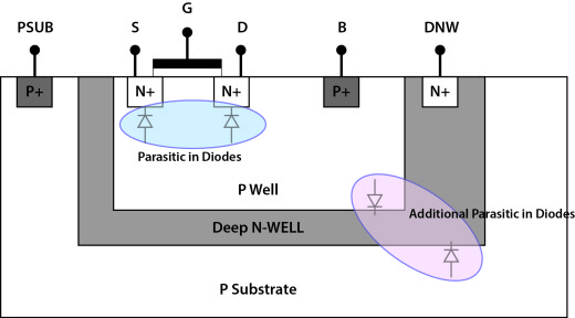
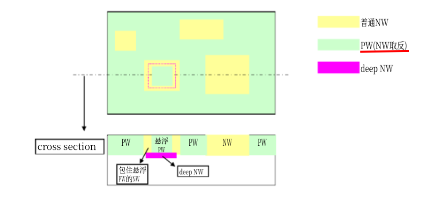
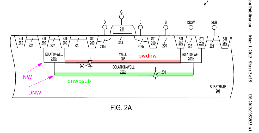
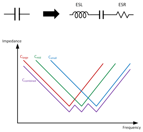
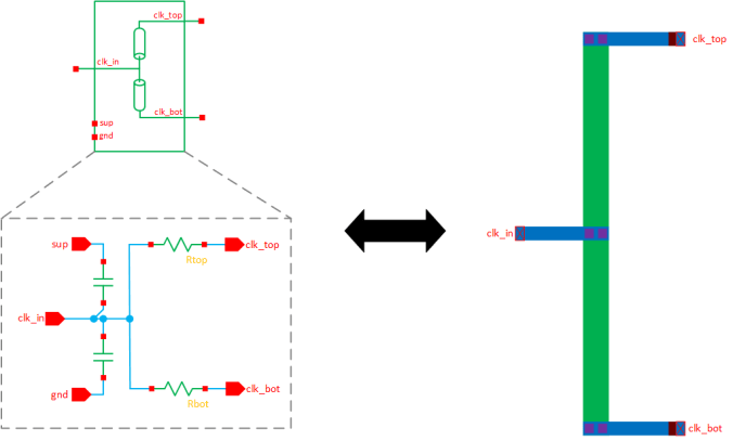
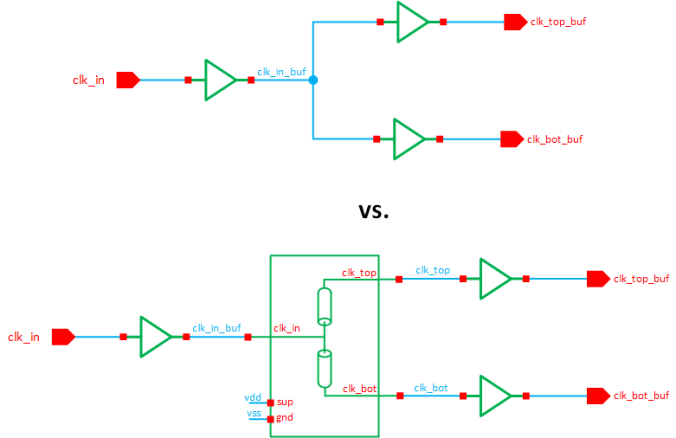
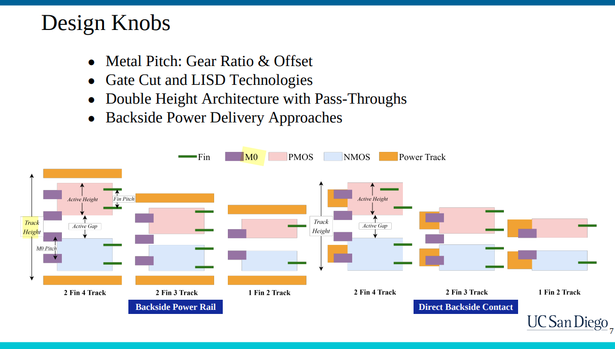
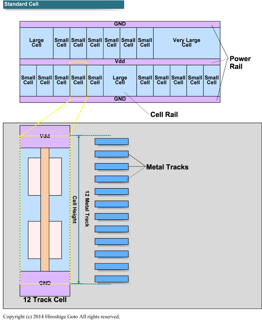
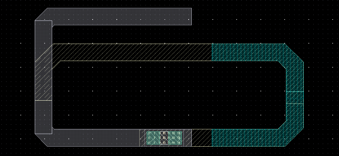
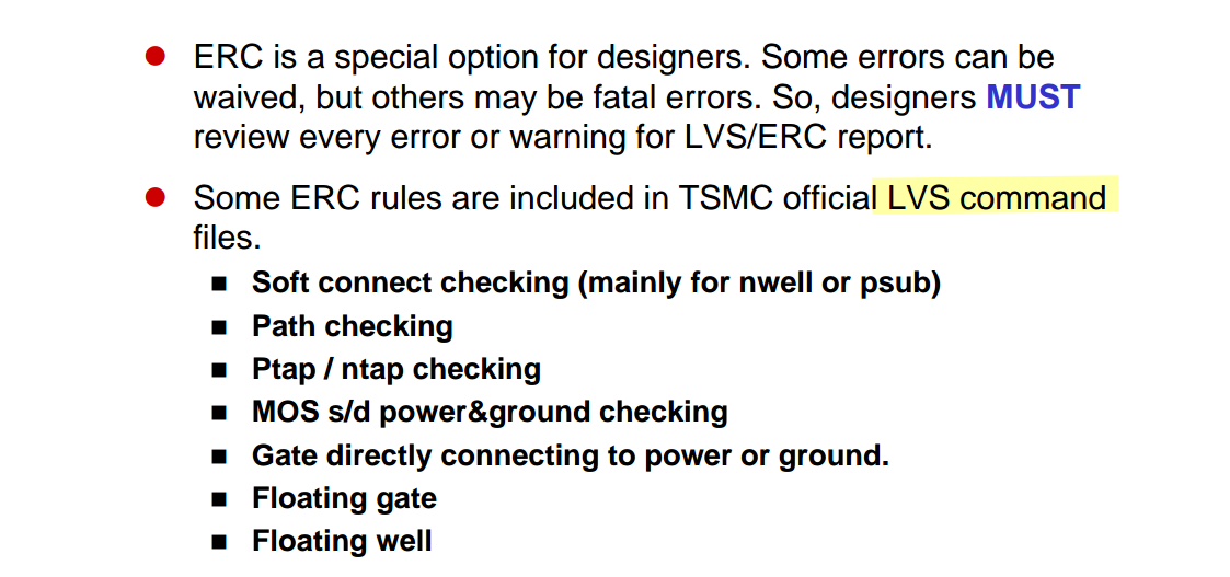

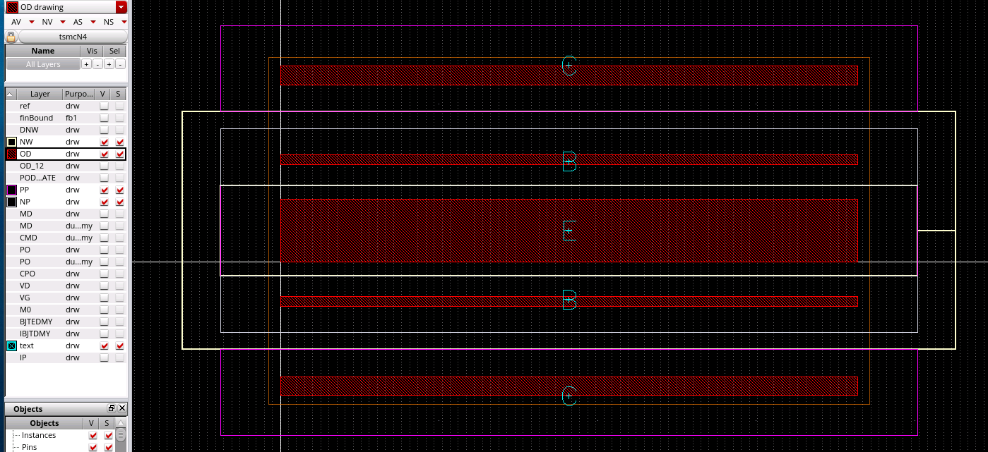
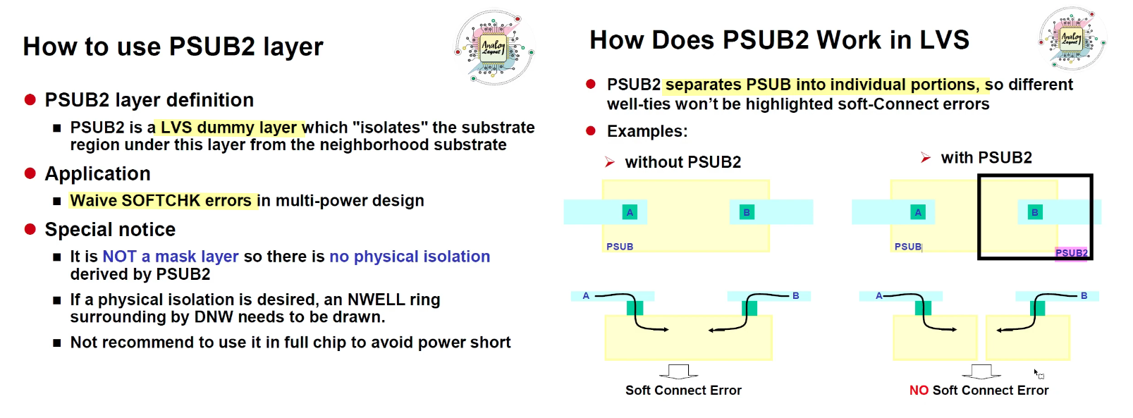
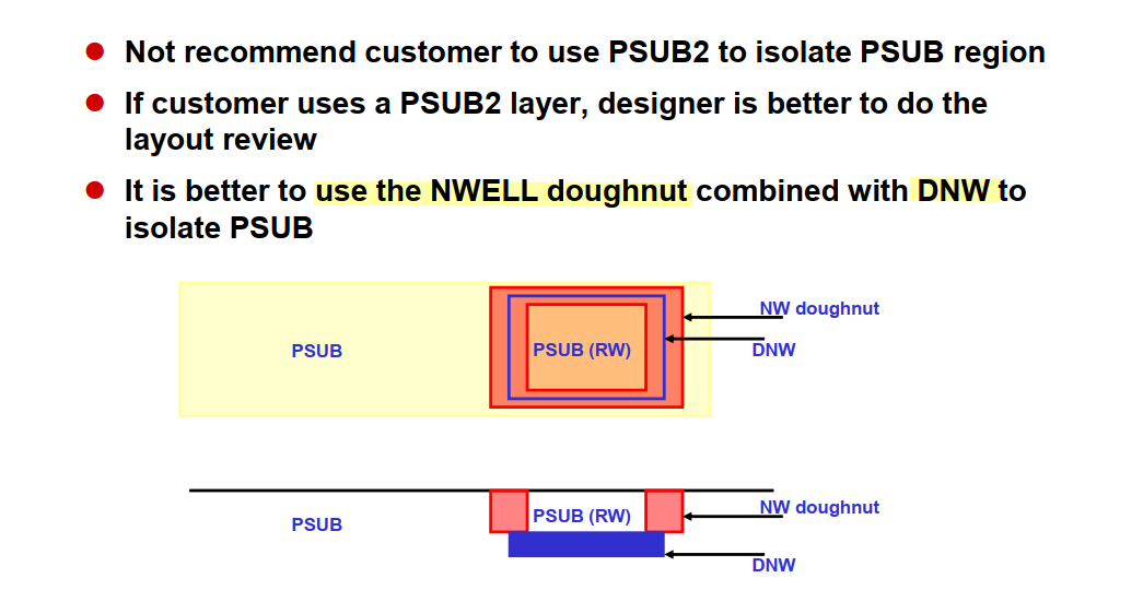
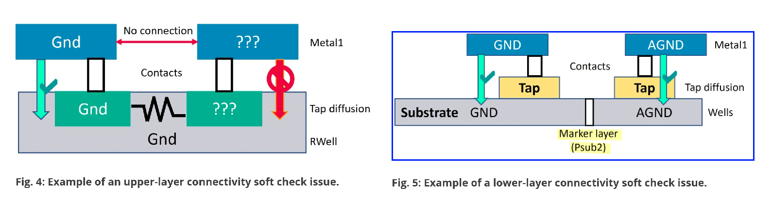
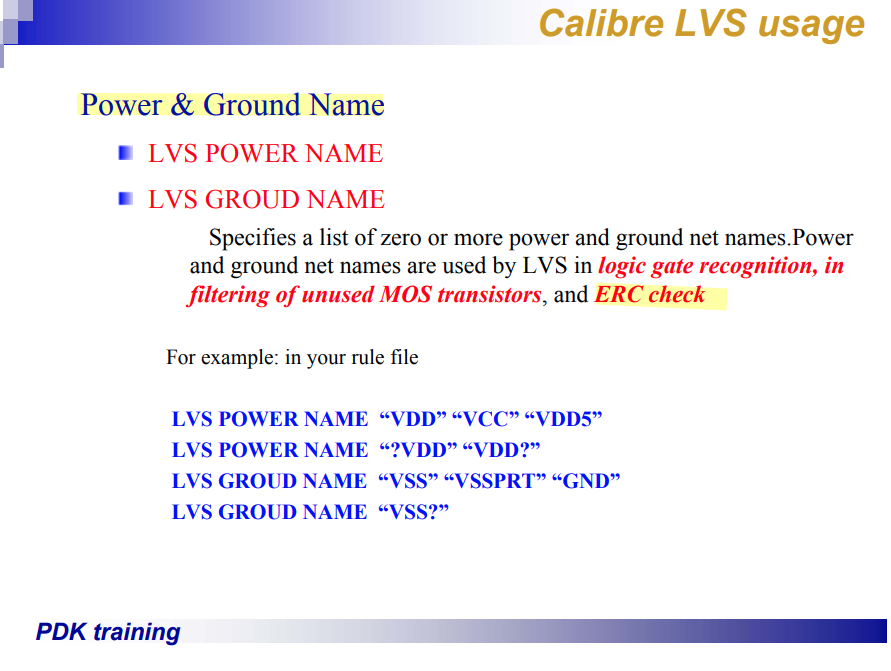

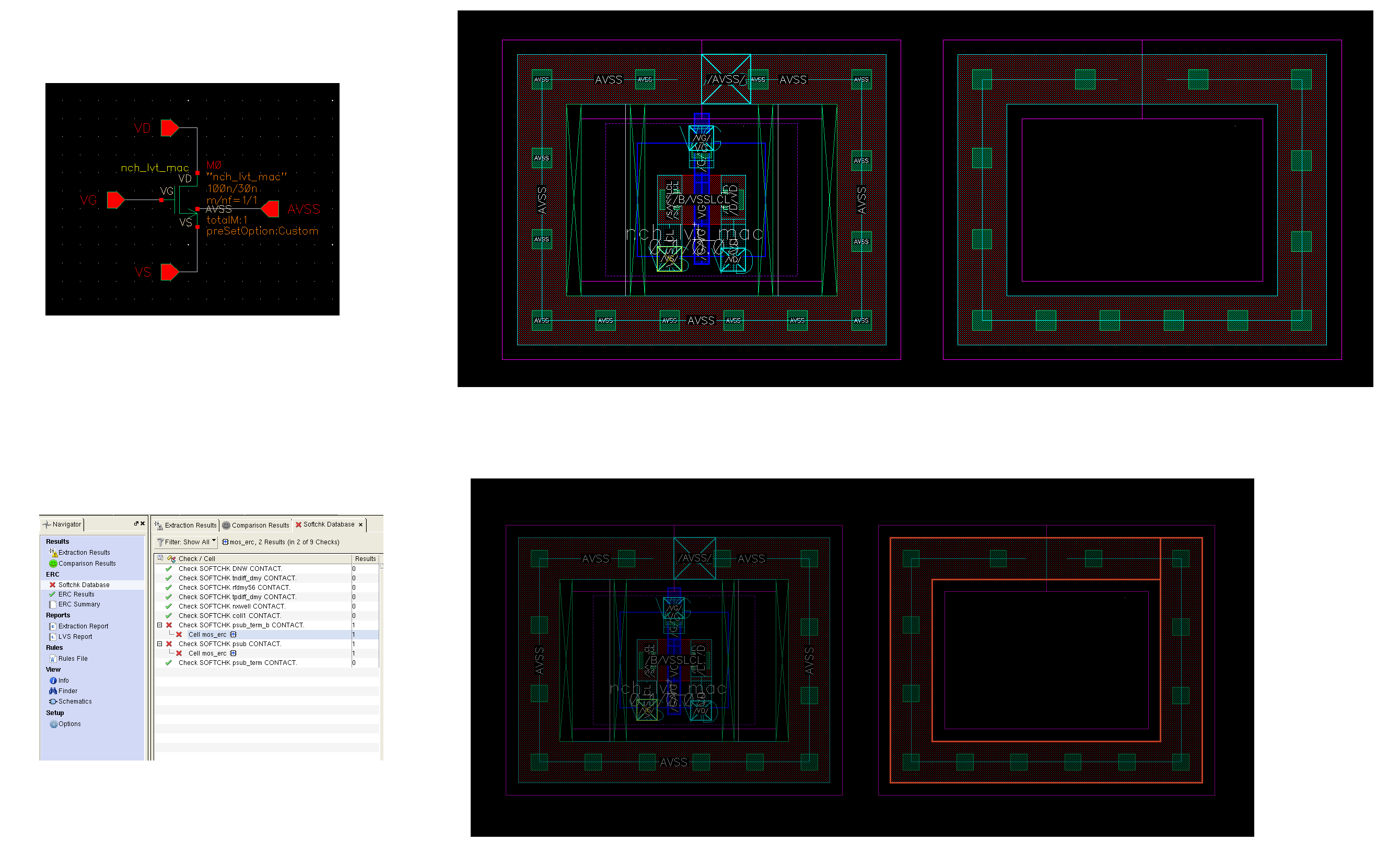
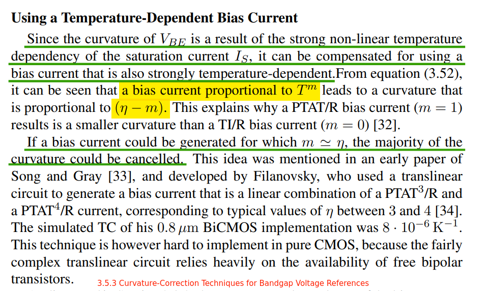
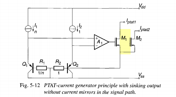
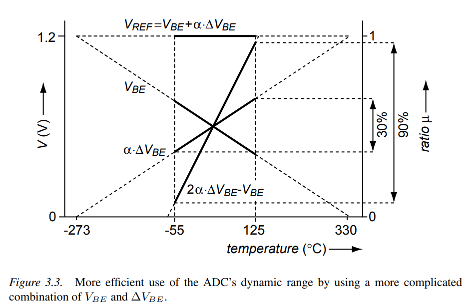
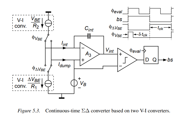
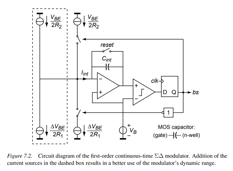
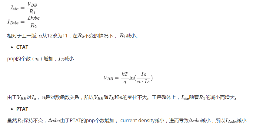
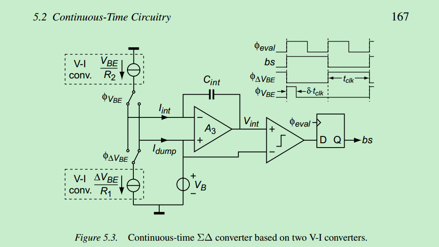
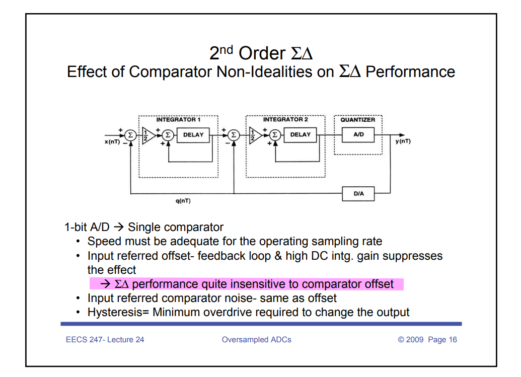
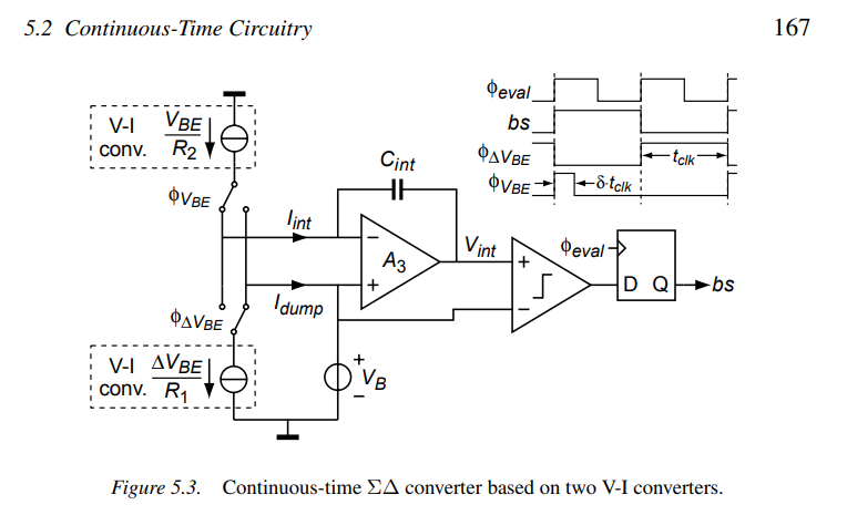
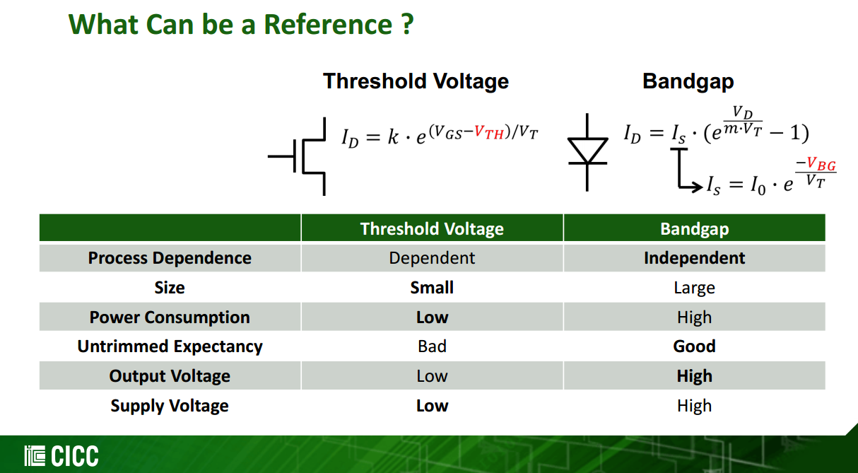
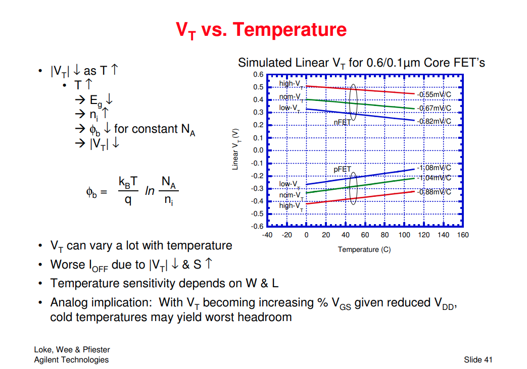
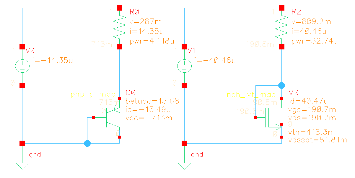
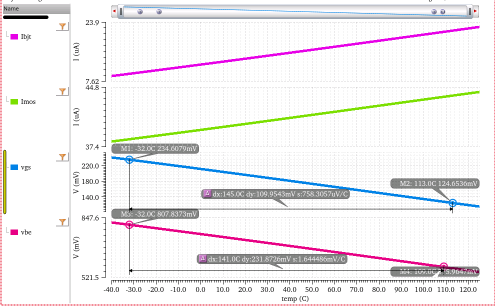
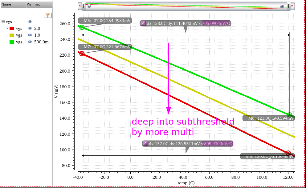
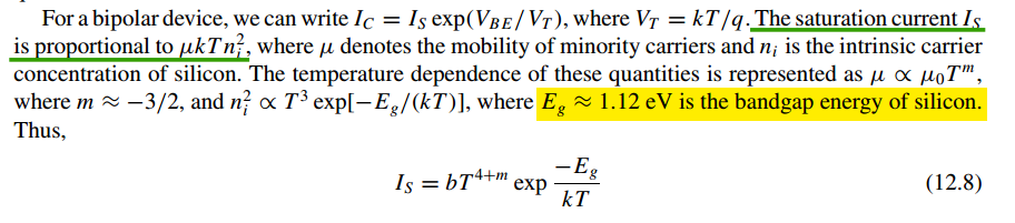
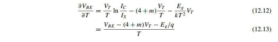
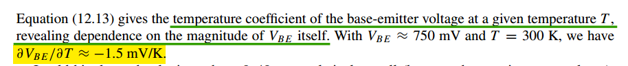

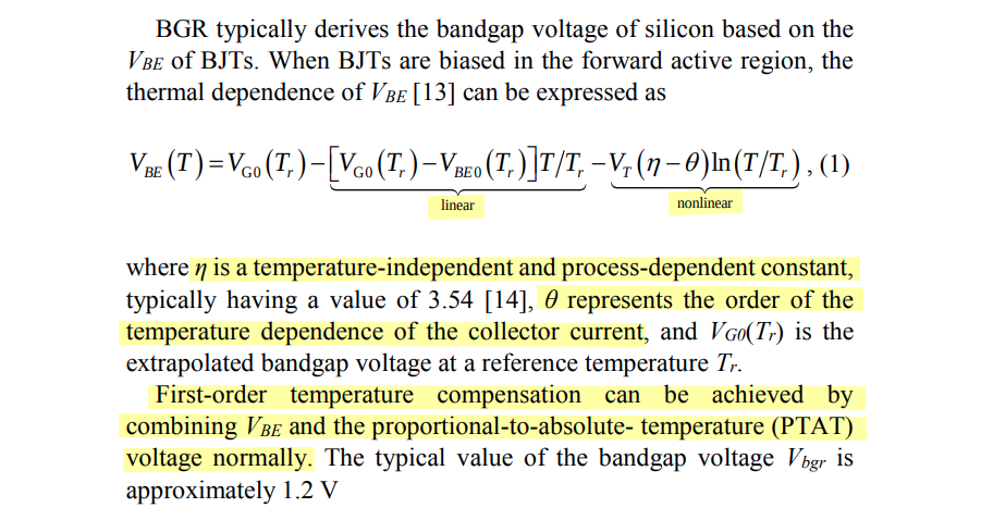
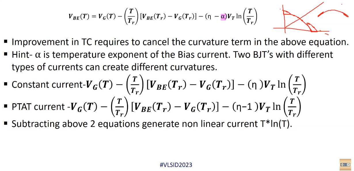
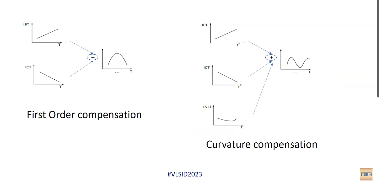
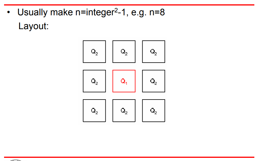


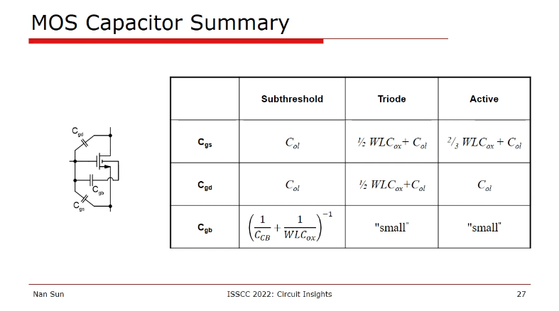
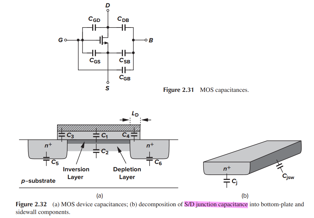
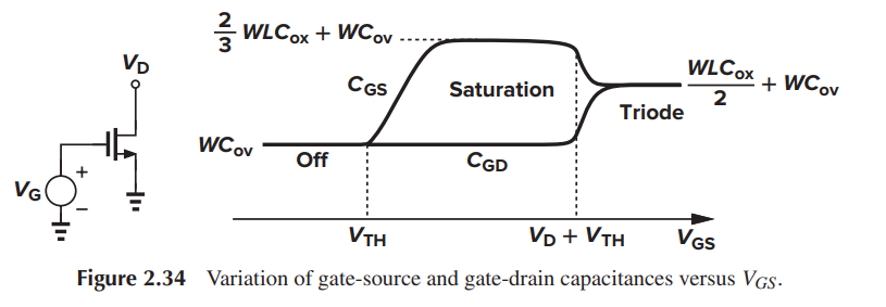
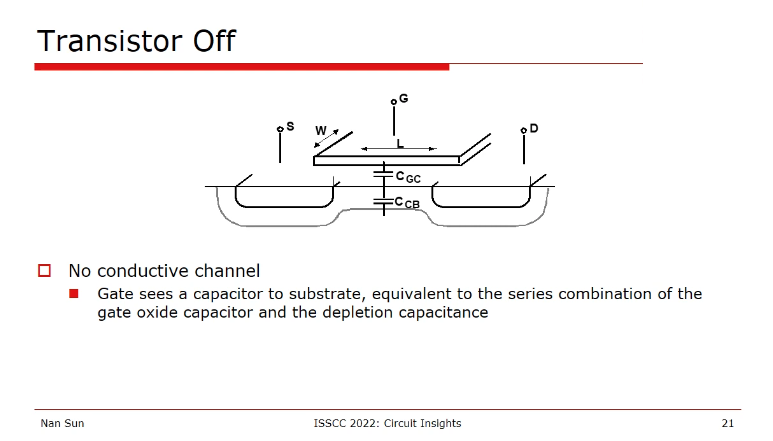
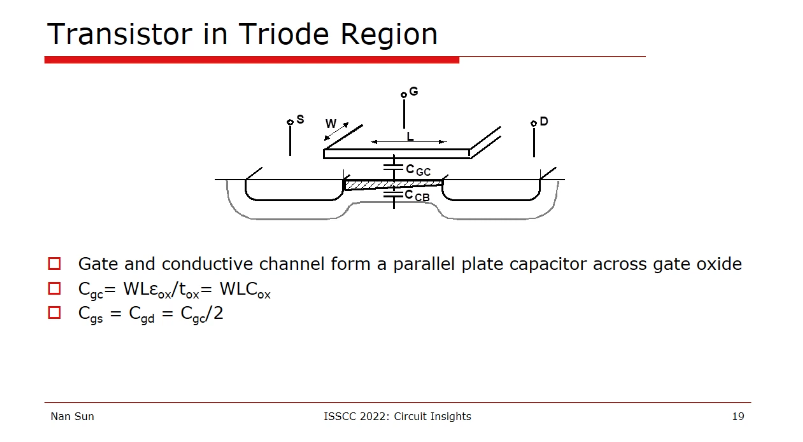
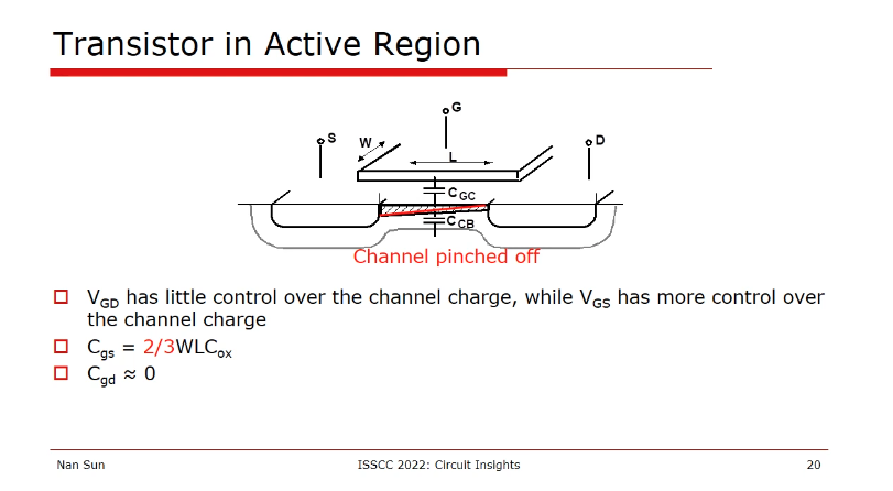
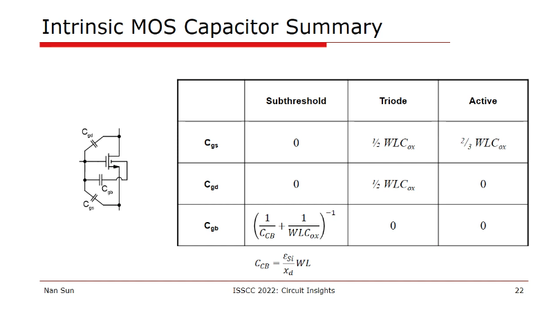
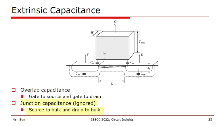
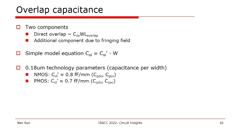
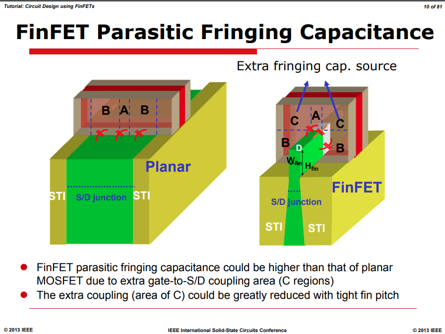
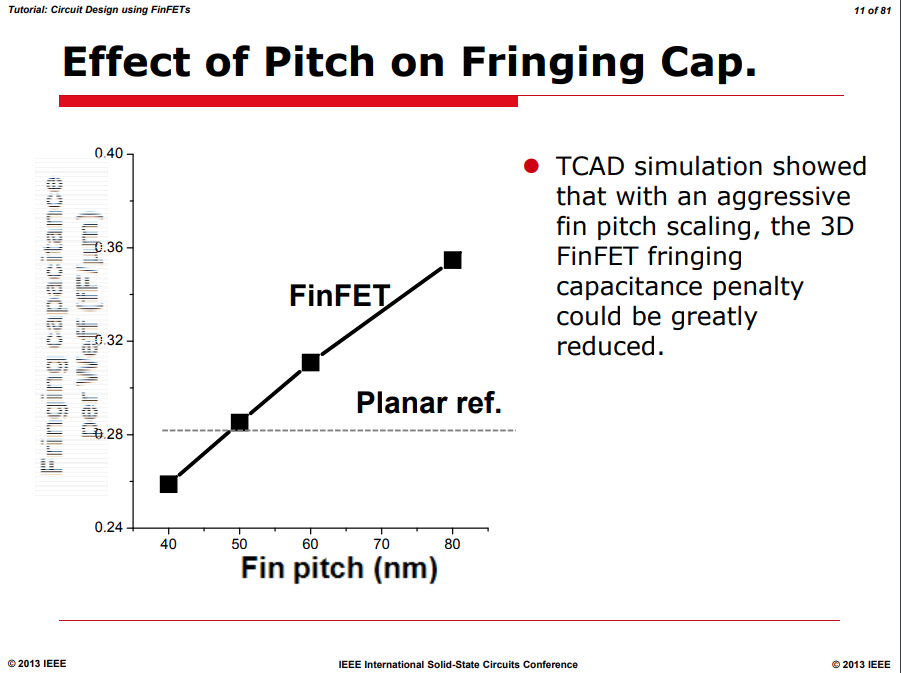
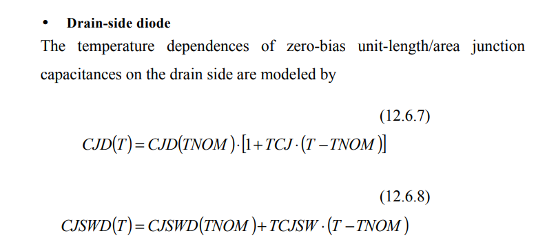
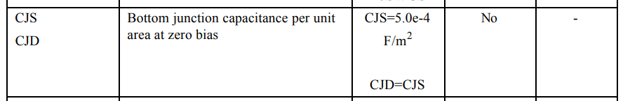
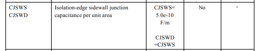
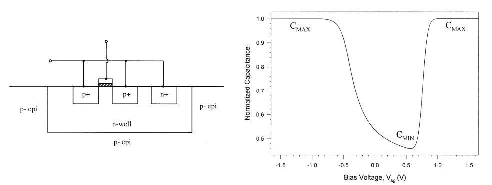
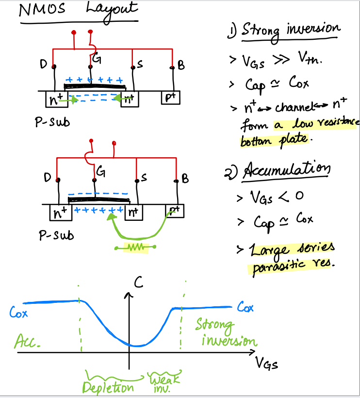
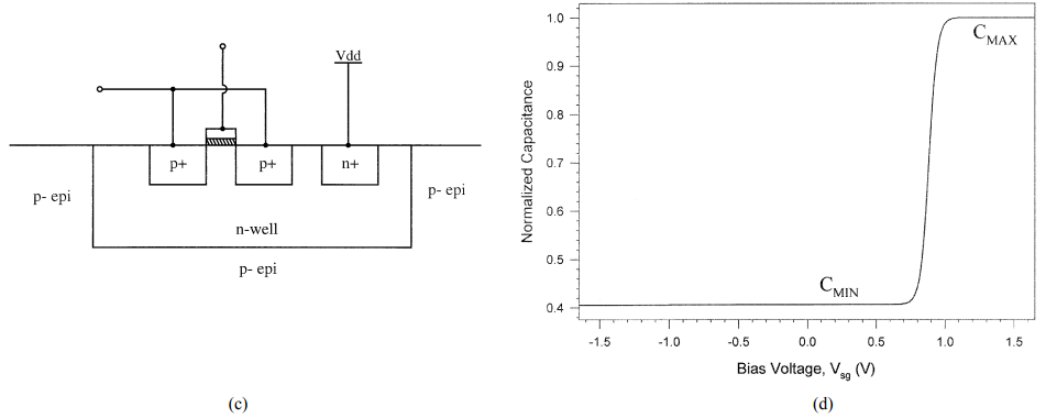
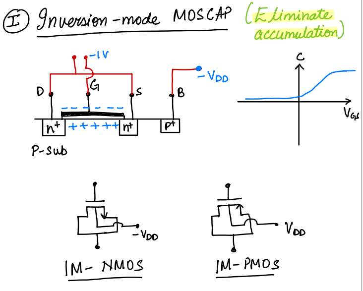
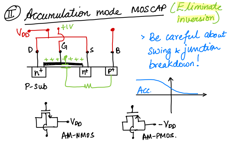
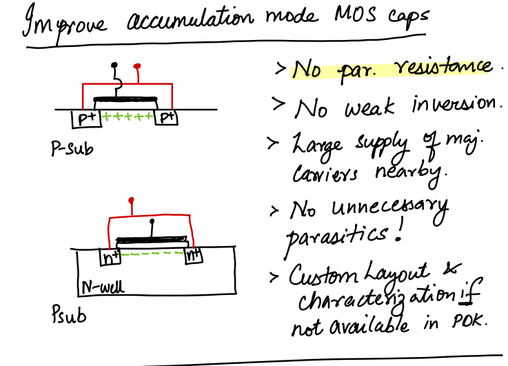
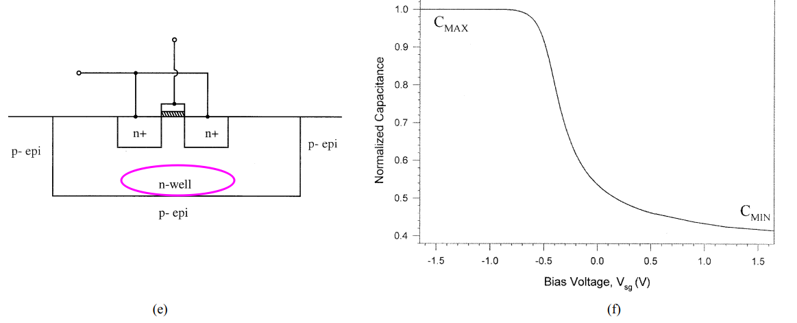
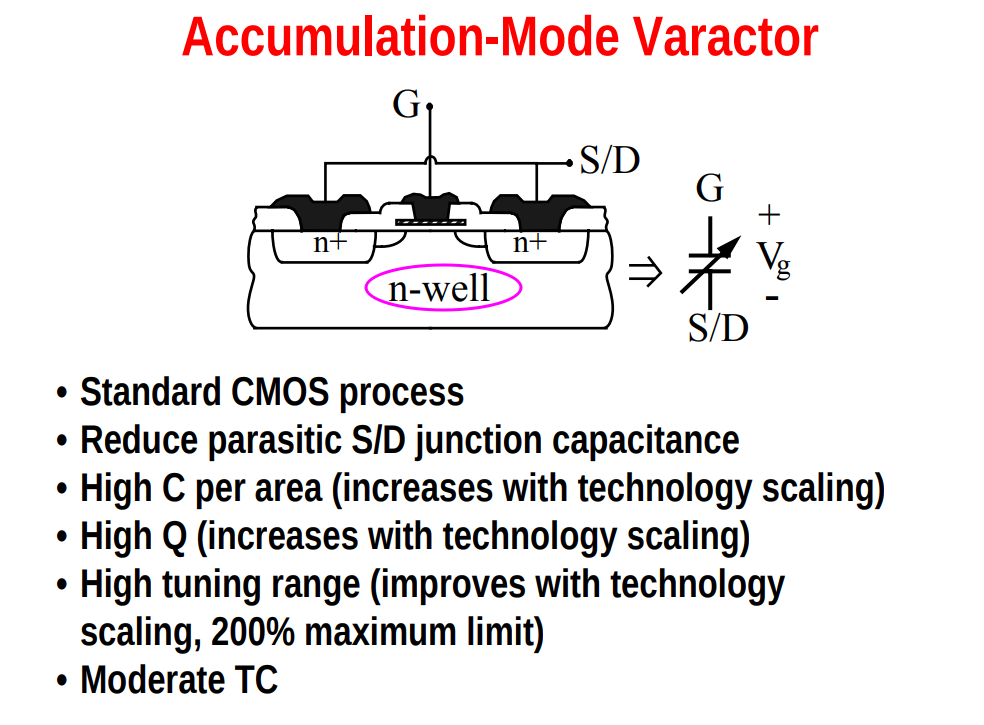
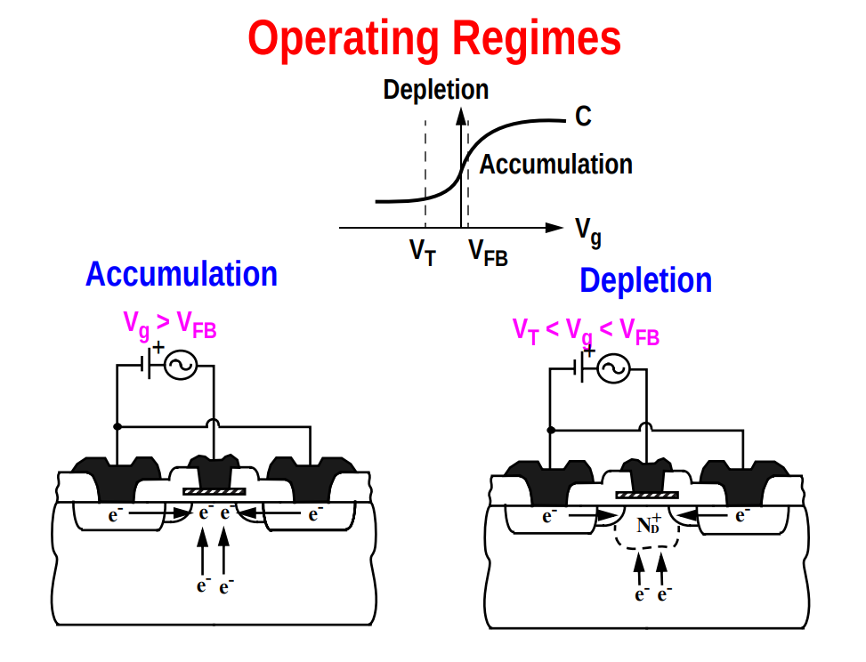
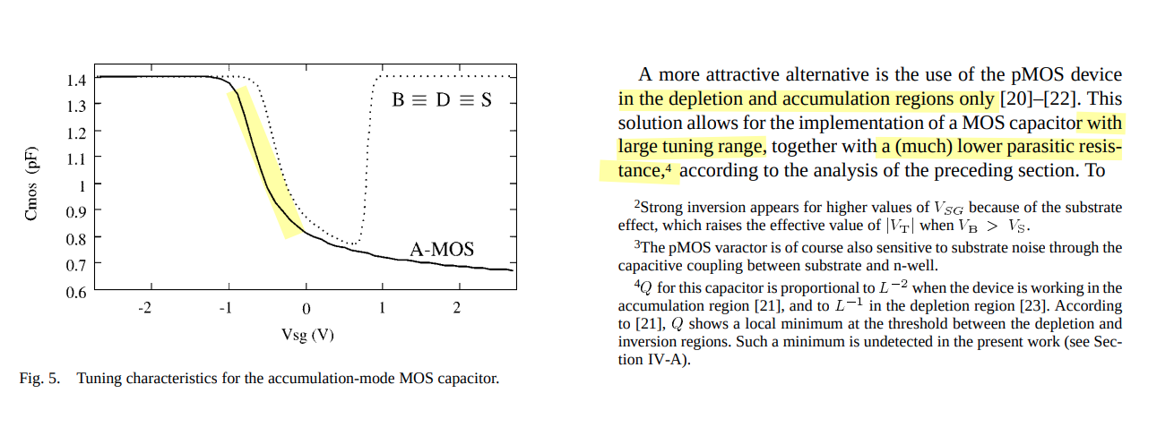
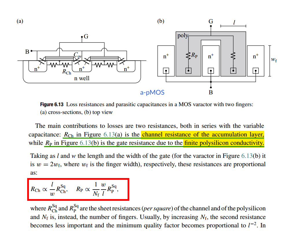
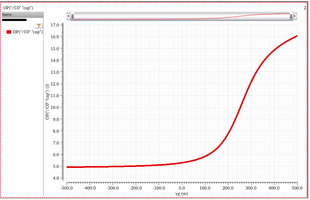
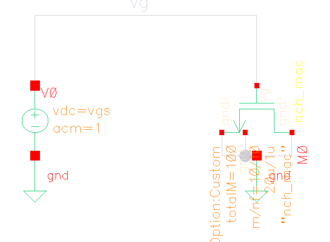
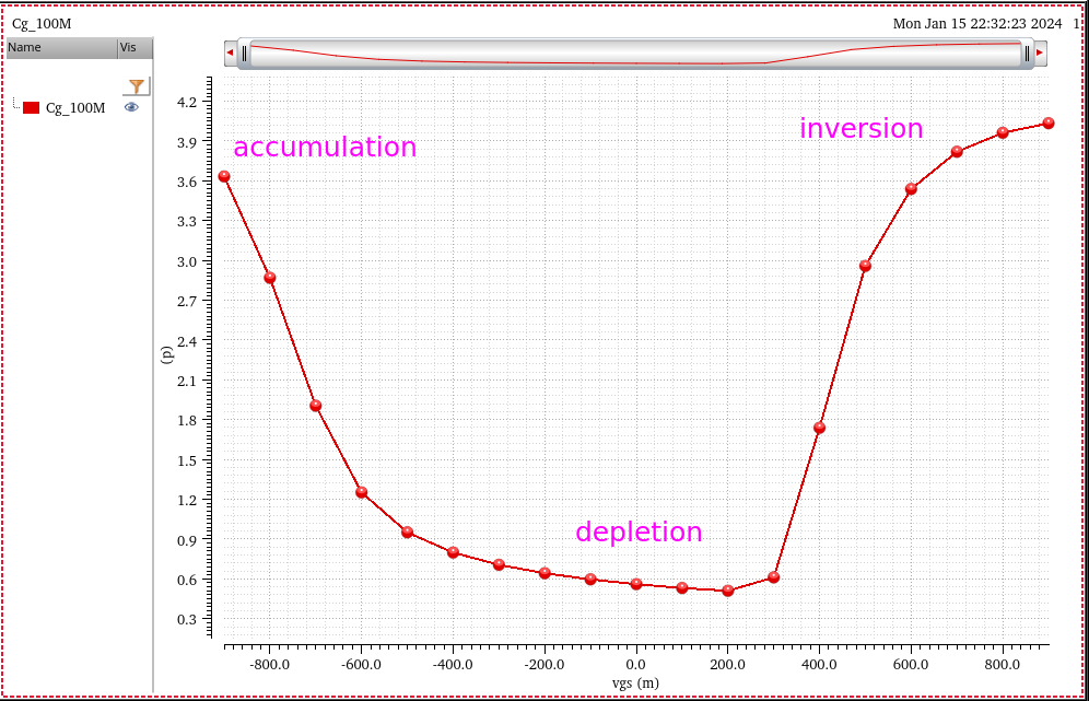
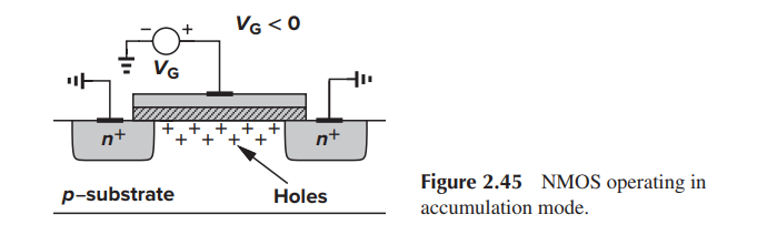
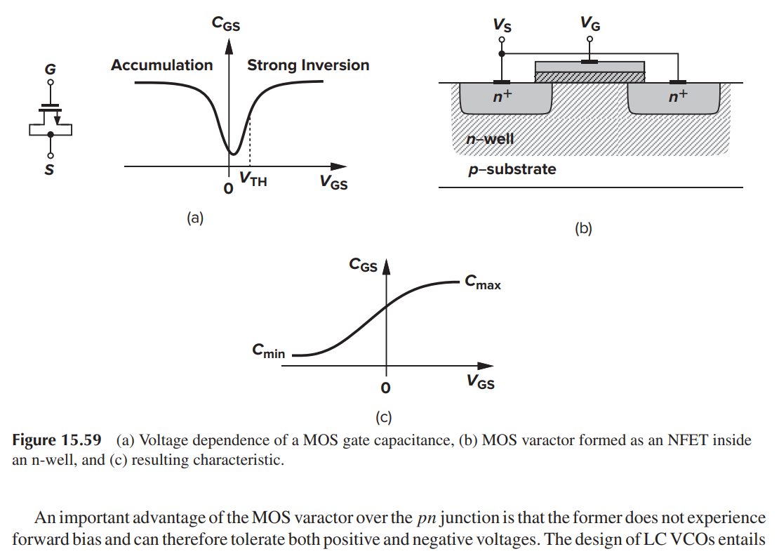
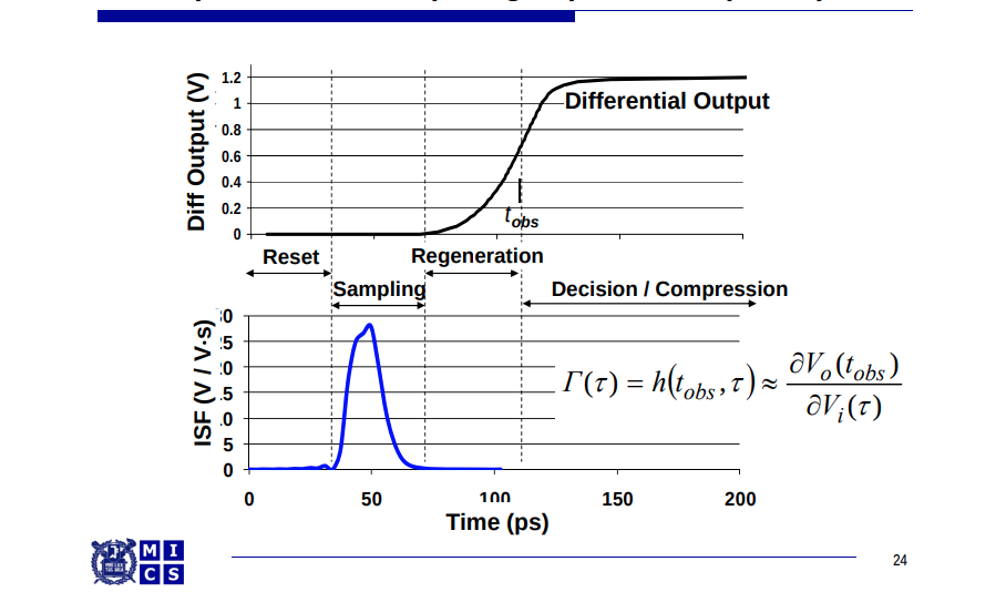
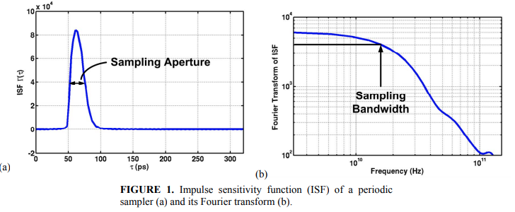

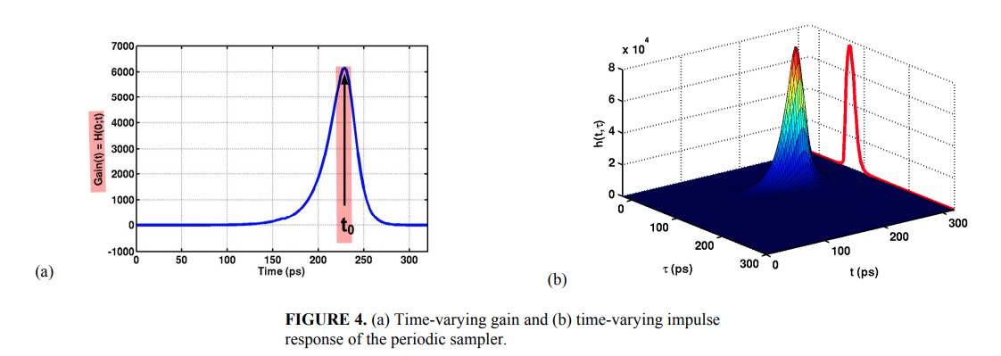
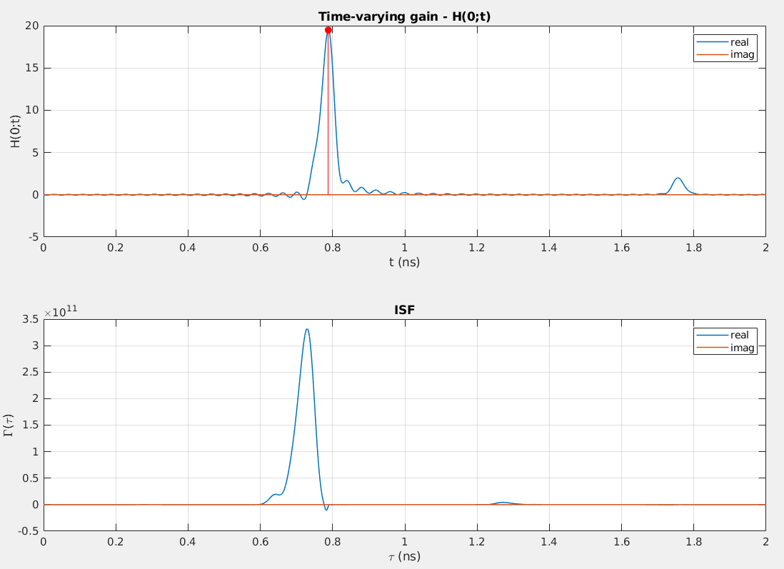
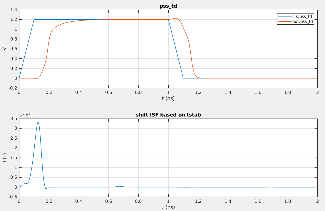
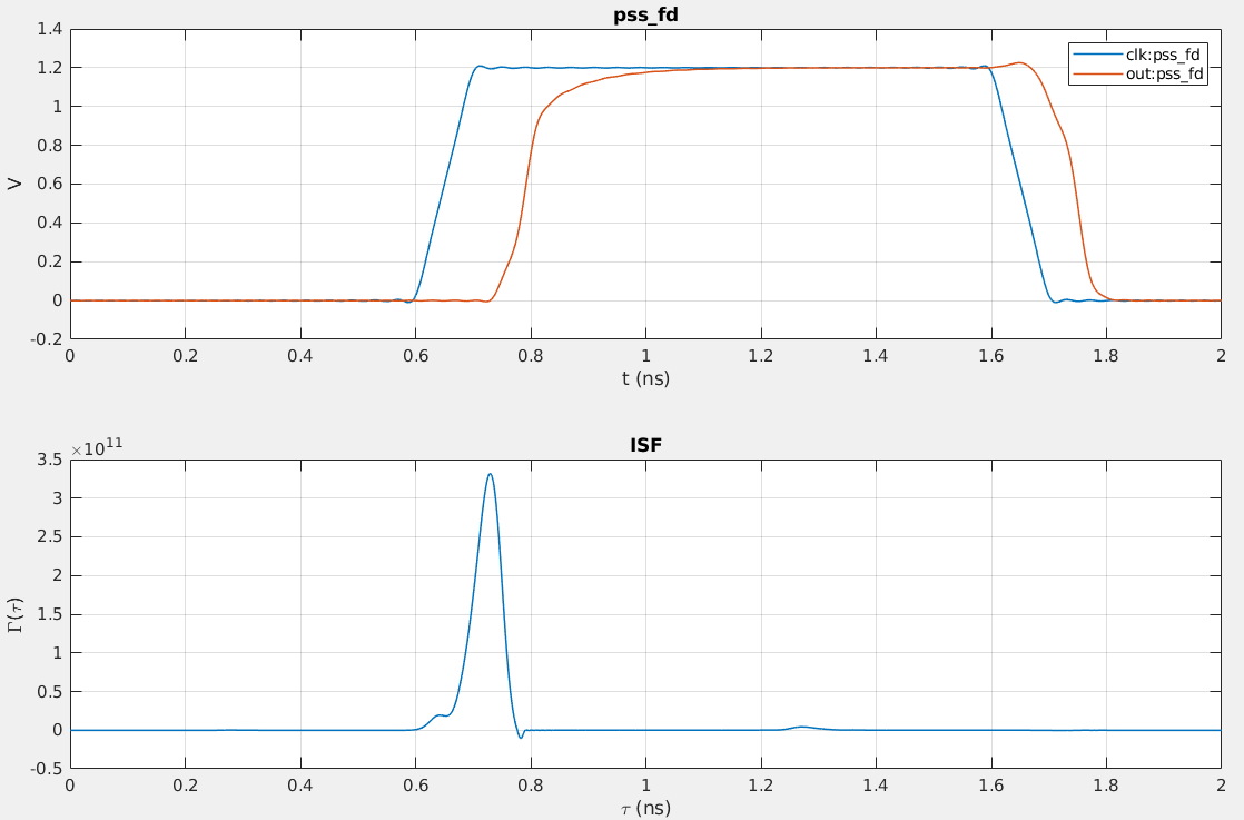
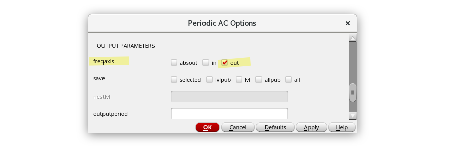
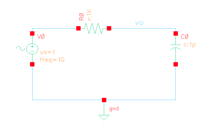
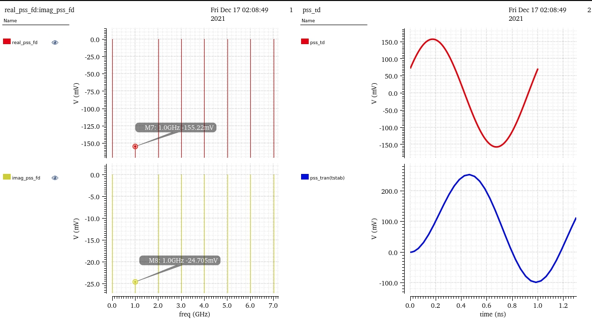
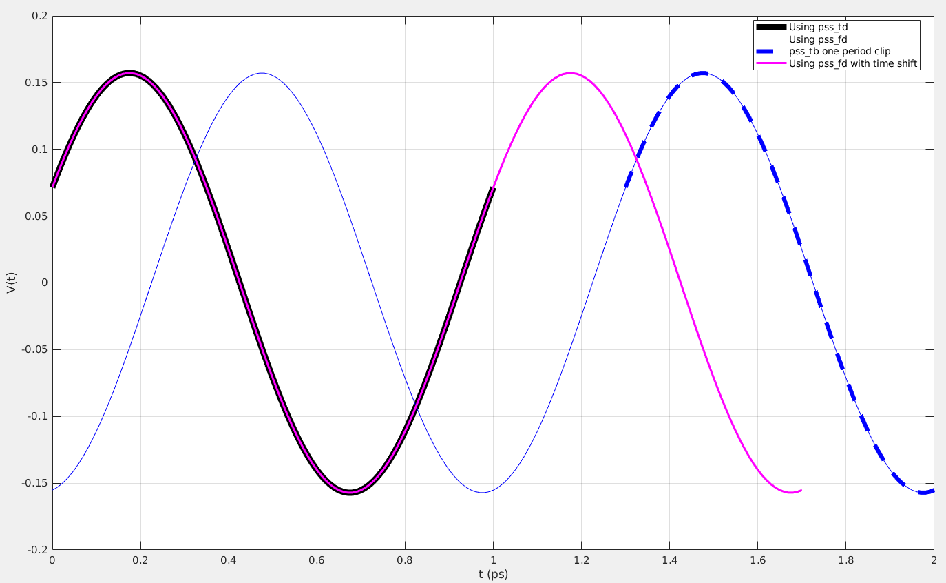
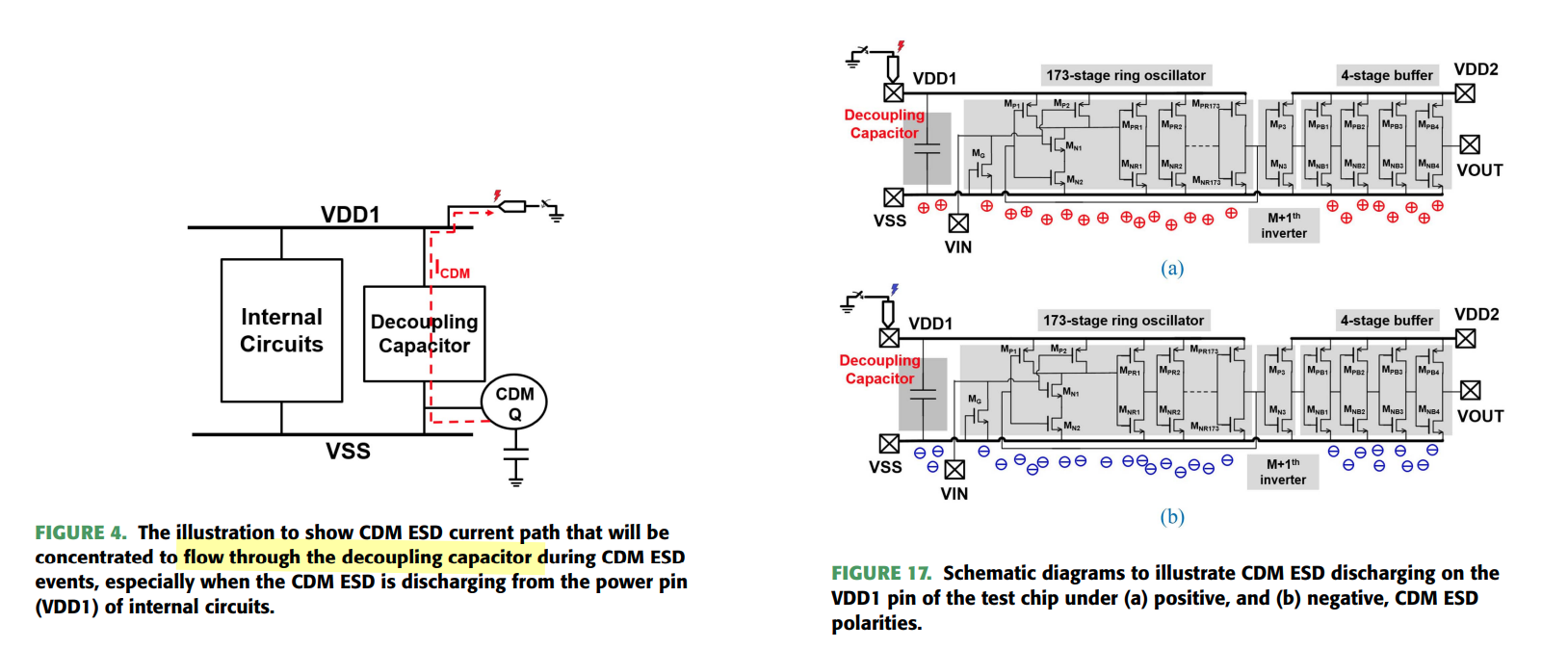
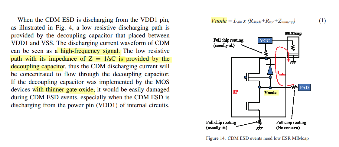
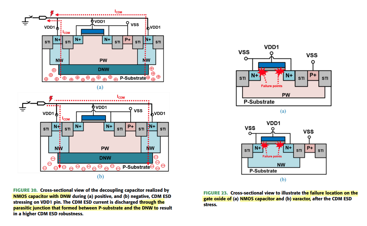
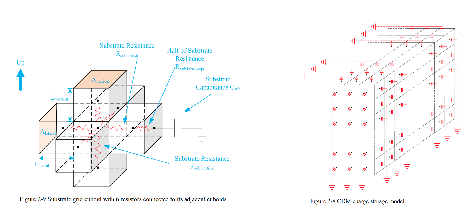
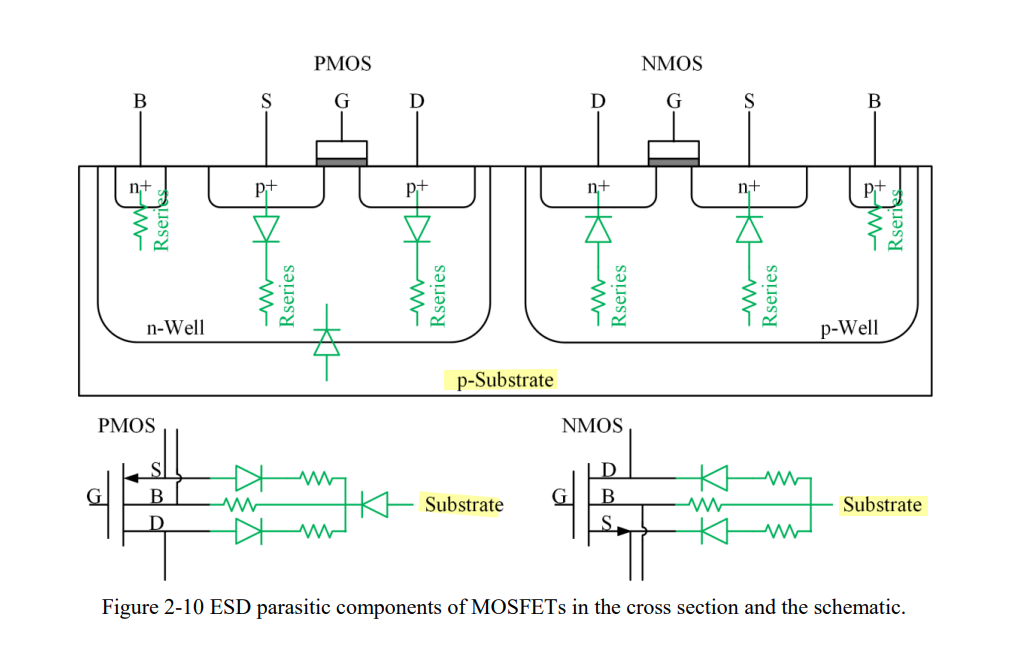
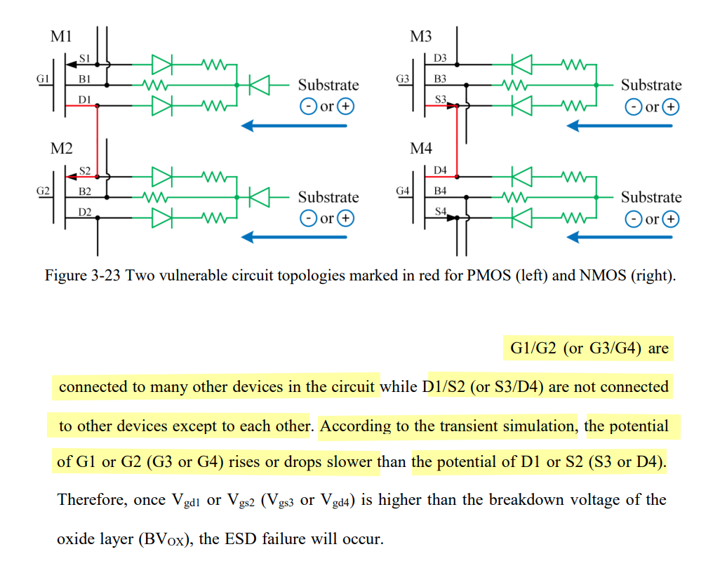
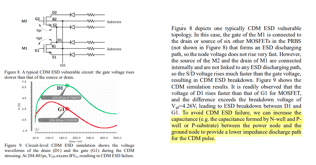
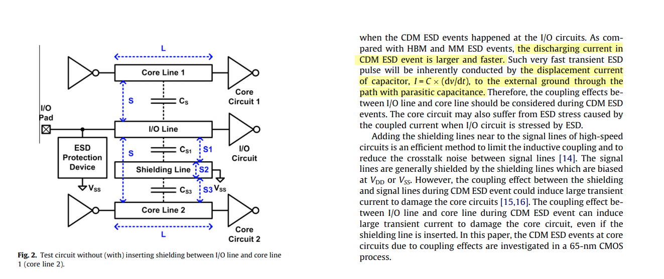
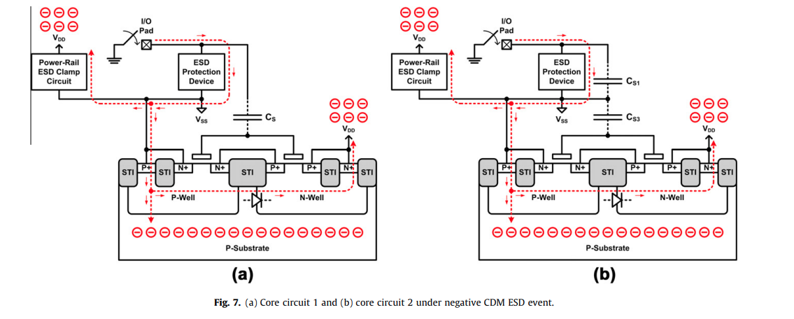
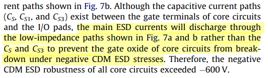
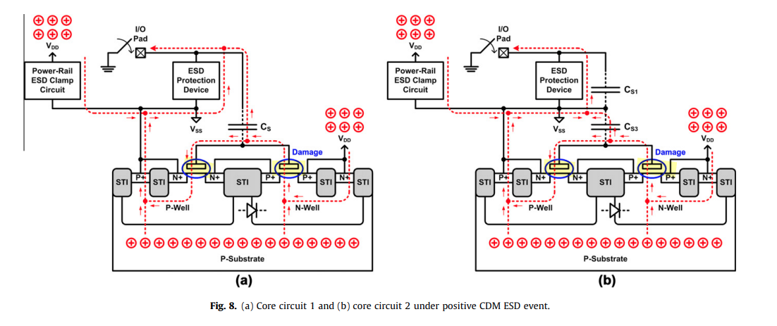
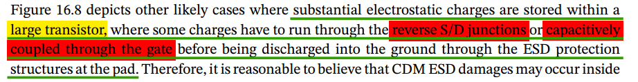
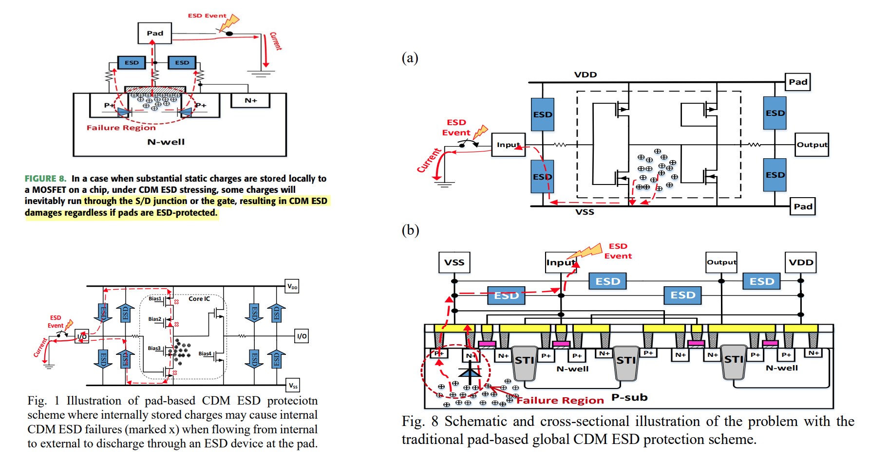
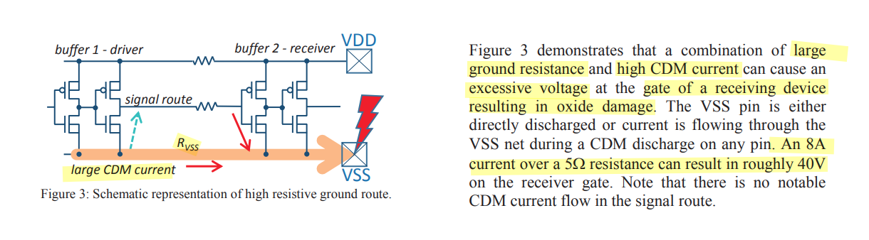
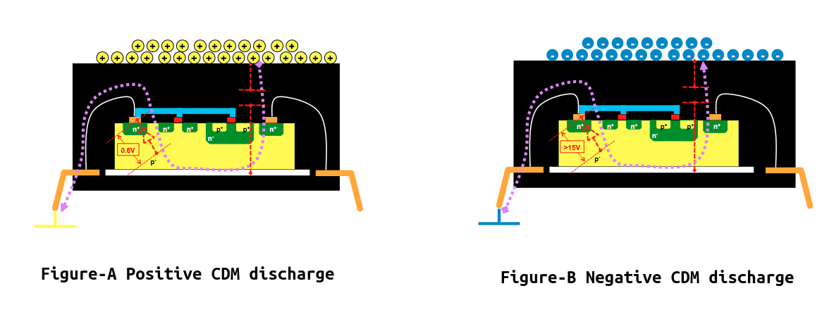
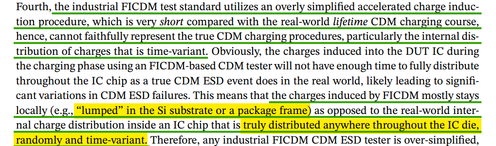
 Confusion about the test procedure is
understandable because the actual process is opposite from what is
expected
Confusion about the test procedure is
understandable because the actual process is opposite from what is
expected