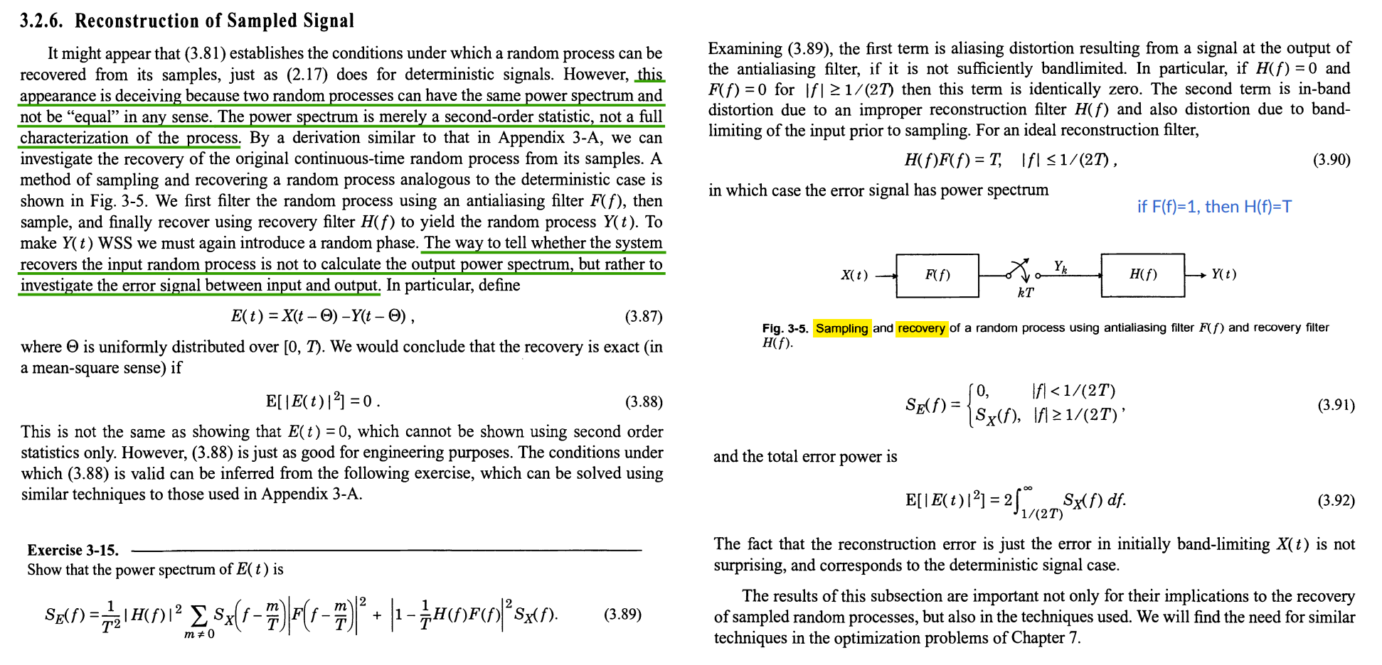
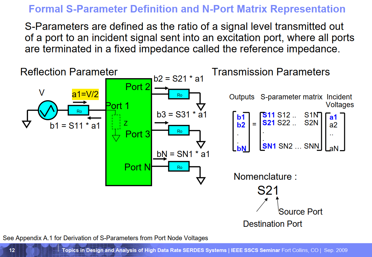
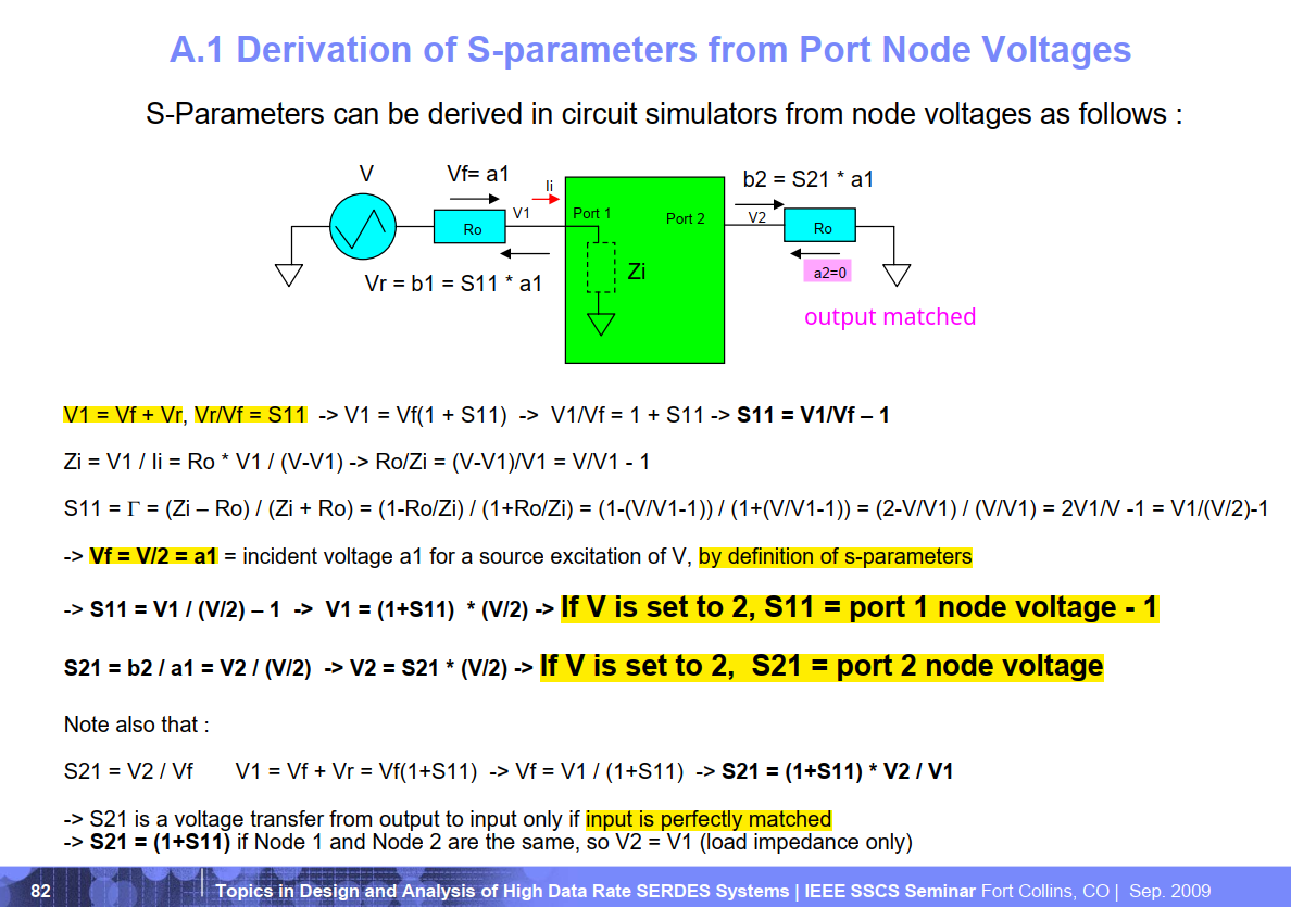
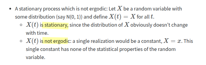
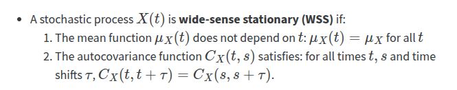
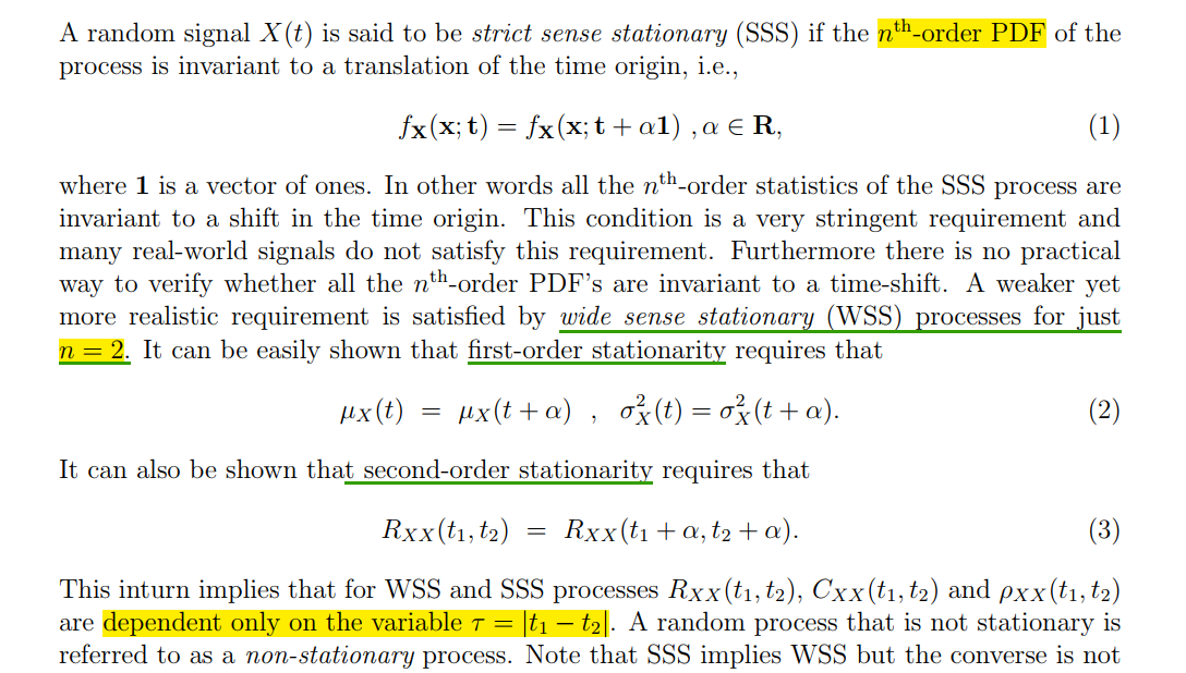
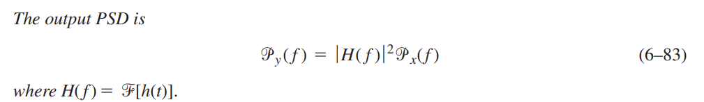
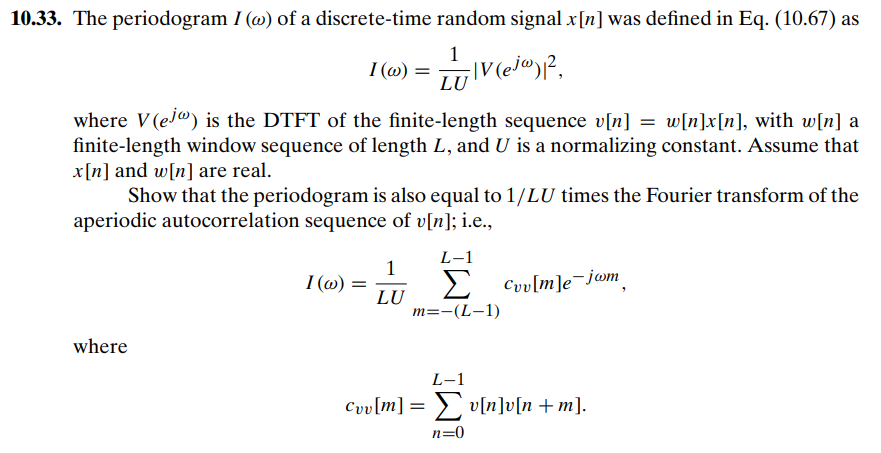
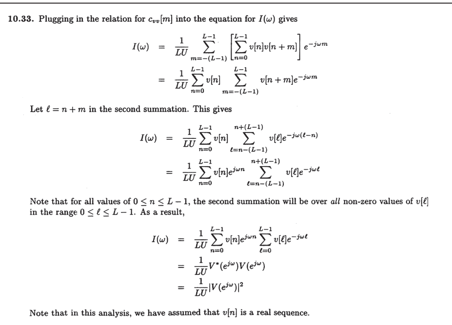
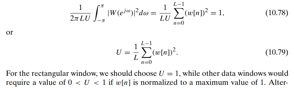
Are AC-Driven Circuits Linear?

\[ f(x_1 + x_2)= f(x_1)+ f(x_2) \]

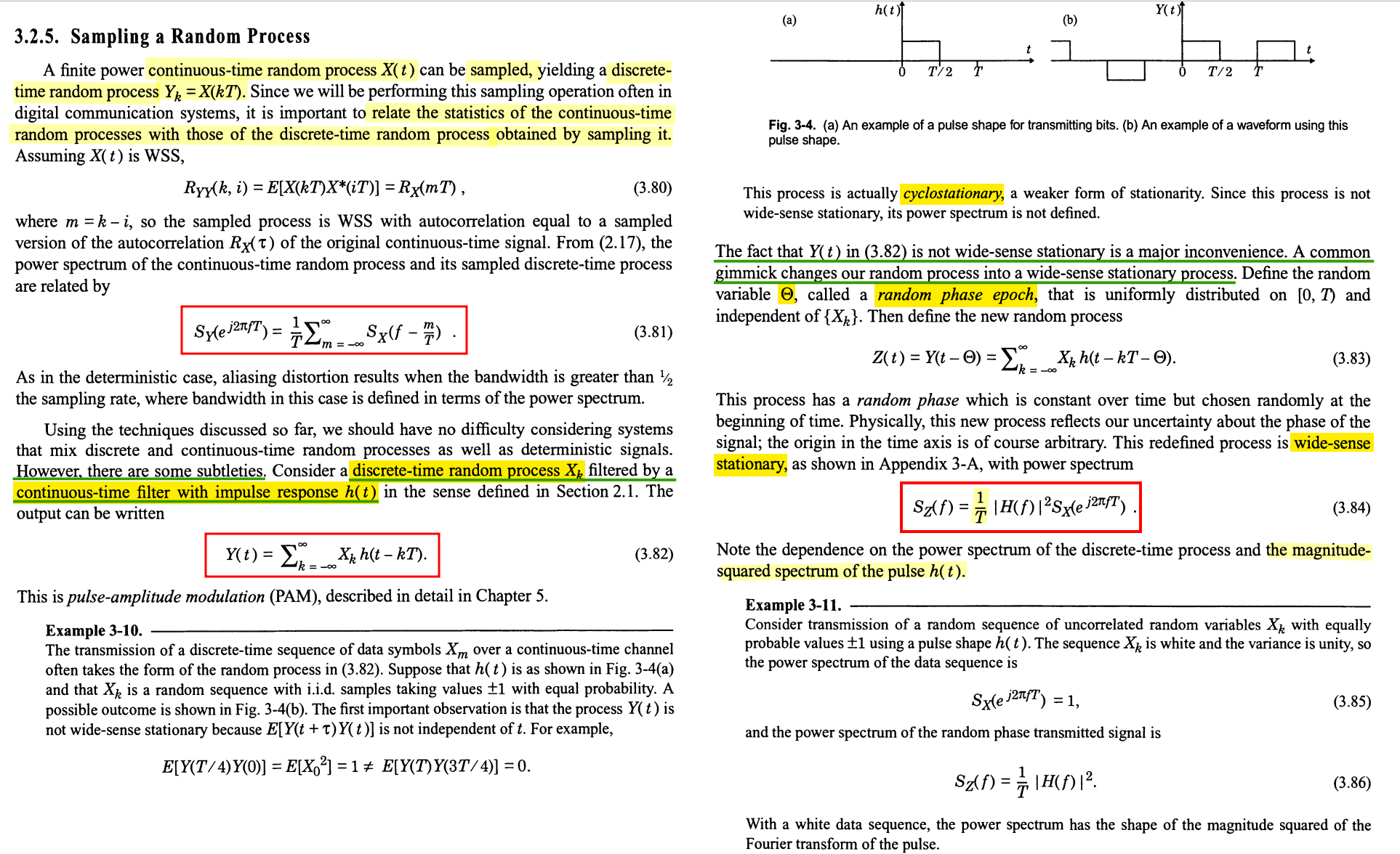
Often, AC-driven circuits can be mistaken as non-linear as the basis that determines the linearity of a circuit is the relationship between the voltage and current.

While an AC signal varies with time, it still exhibits a linear relationship across elements like resistors, capacitors, and inductors. Therefore, AC driven circuits are linear.
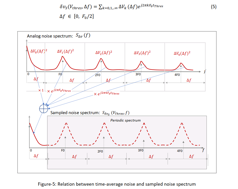
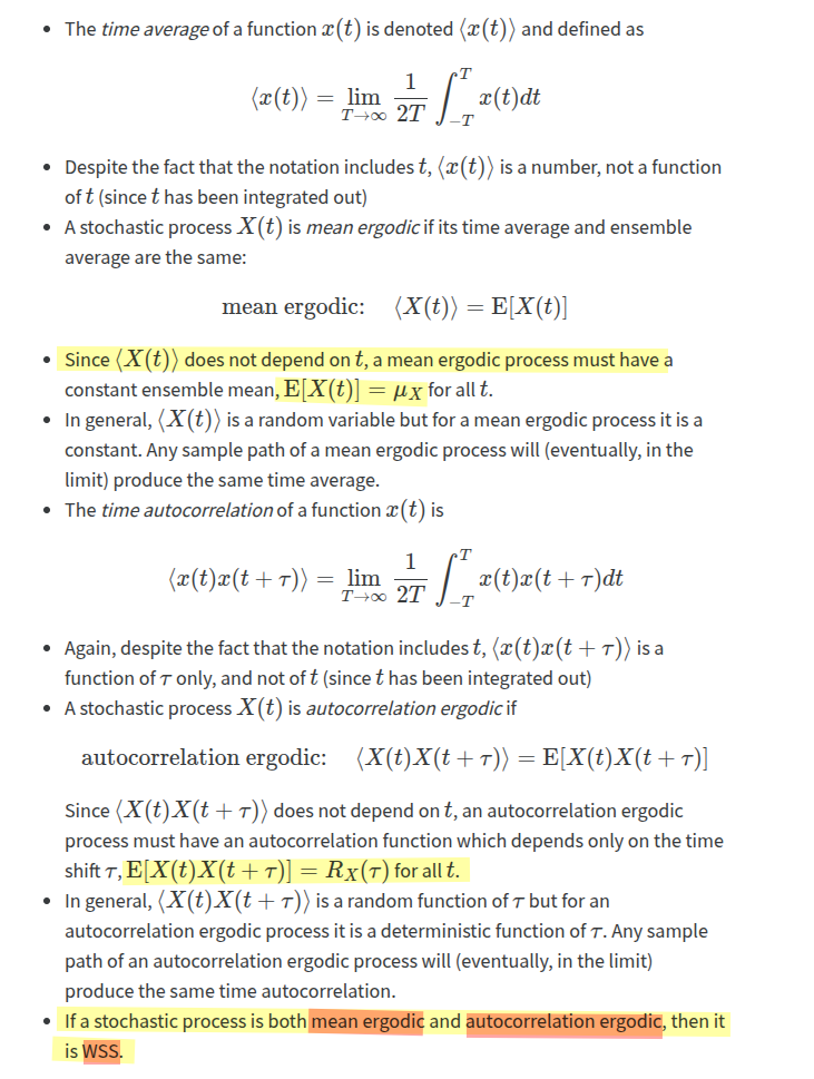
Phasor

Phasor concept has no real physical significance. It is just a convenient mathematical tool.

Phasor analysis determines the steady-state response to a linear circuit driven by sinusoidal sources with frequency \(f\)

If your circuit includes transistors or other nonlinear components, all is not lost. There is an extension of phasor analysis to nonlinear circuits called small-signal analysis in which you linearize the components before performing phasor analysis - AC analyses of SPICE

A sinusoid is characterized by 3 numbers, its amplitude, its phase, and its frequency. For example \[ v(t) = A\cos(\omega t + \phi) \tag{1} \] In a circuit there will be many signals but in the case of phasor analysis they will all have the same frequency. For this reason, the signals are characterized using only their amplitude and phase.

The combination of an amplitude and phase to describe a signal is the phasor for that signal.

Thus, the phasor for the signal in \((1)\) is \(A\angle \phi\)

In general, phasors are functions of frequency

Often it is preferable to represent a phasor using complex numbers rather than using amplitude and phase. In this case we represent the signal as: \[ v(t) = \Re\{Ve^{j\omega t} \} \tag{2} \] where \(V=Ae^{j\phi}\) is the phasor.

\((1)\) and \((2)\) are the same

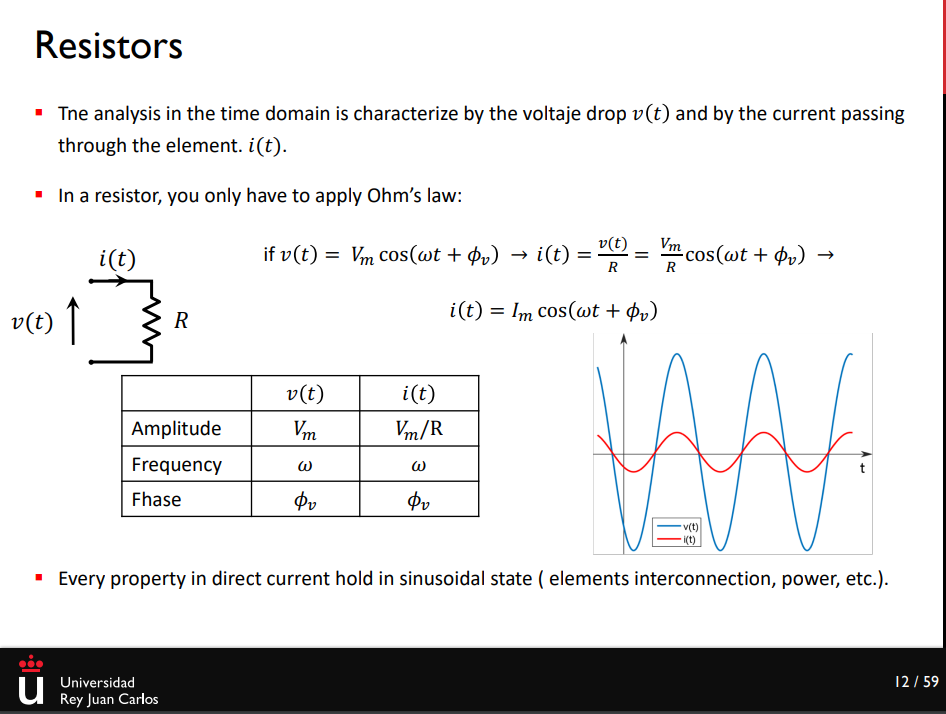
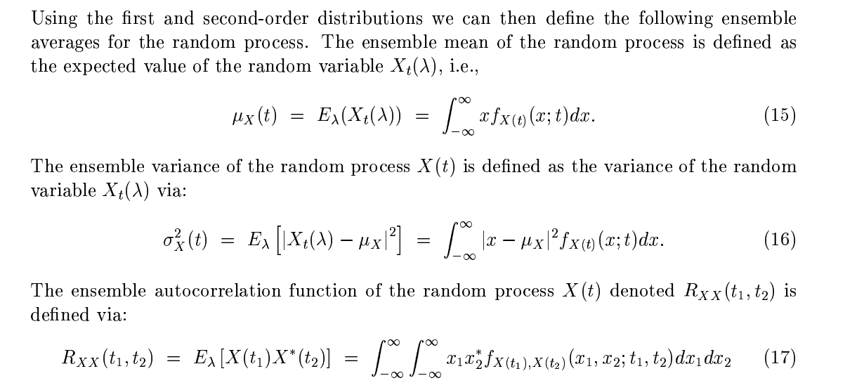
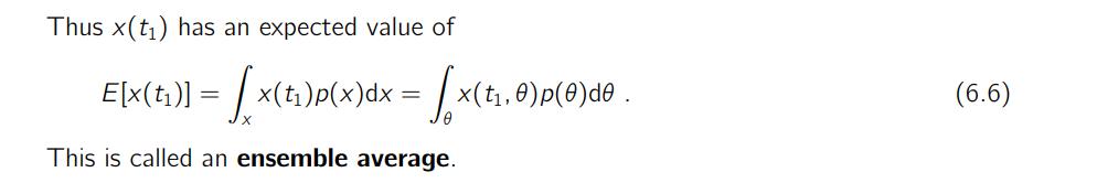
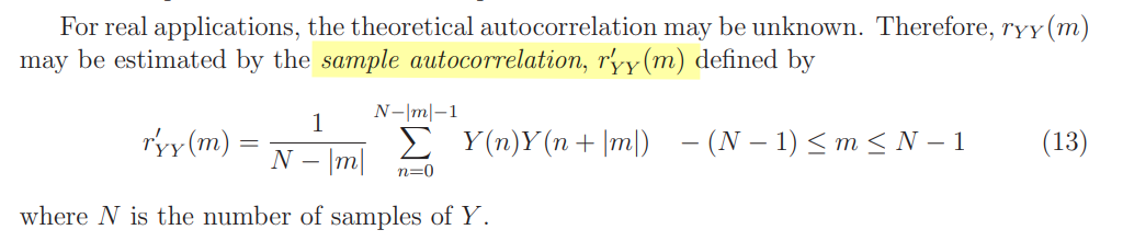
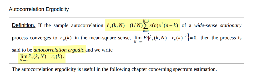
Phasor Model of a Resistor

A linear resistor is defined by the equation \(v = Ri\)

Now, assume that the resistor current is described with the phasor \(I\). Then \[ i(t) = \Re\{Ie^{j\omega t}\} \] \(R\) is a real constant, and so the voltage can be computed to be \[ v(t) = R\Re\{Ie^{j\omega t}\} = \Re\{RIe^{j\omega t}\} = \Re\{Ve^{j\omega t}\} \] where \(V\) is the phasor representation for \(v\), i.e. \[ V = RI \]

  1. Thus, given the phasor for the current we can directly compute the phasor for the voltage across the resistor.

  2. Similarly, given the phasor for the voltage across a resistor we can compute the phasor for the current through the resistor using \(I = \frac{V}{R}\)

Phasor Model of a Capacitor

A linear capacitor is defined by the equation \(i=C\frac{\mathrm{d}v}{\mathrm{d}t}\)

Now, assume that the voltage across the capacitor is described with the phasor \(V\). Then \[ v(t) = \Re\{ V e^{j\omega t}\} \] \(C\) is a real constant \[ i(t) = C\Re\{\frac{\mathrm{d}}{\mathrm{d}t}V e^{j\omega t}\} = \Re\{j\omega C V e^{j\omega t}\} \] The phasor representation for \(i\) is \(i(t) = \Re\{Ie^{j\omega t}\}\), that is \(I = j\omega C V\)

  1. Thus, given the phasor for the voltage across a capacitor we can directly compute the phasor for the current through the capacitor.

  2. Similarly, given the phasor for the current through a capacitor we can compute the phasor for the voltage across the capacitor using \(V=\frac{I}{j\omega C}\)

Phasor Model of an Inductor

A linear inductor is defined by the equation \(v=L\frac{\mathrm{d}i}{\mathrm{d}t}\)

Now, assume that the inductor current is described with the phasor \(I\). Then \[ i(t) = \Re\{ I e^{j\omega t}\} \] \(L\) is a real constant, and so the voltage can be computed to be \[ v(t) = L\Re\{\frac{\mathrm{d}}{\mathrm{d}t}I e^{j\omega t}\} = \Re\{j\omega L I e^{j\omega t}\} \] The phasor representation for \(v\) is \(v(t) = \Re\{Ve^{j\omega t}\}\), that is \(V = j\omega L I\)

  1. Thus, given the phasor for the current we can directly compute the phasor for the voltage across the inductor.

  2. Similarly, given the phasor for the voltage across an inductor we can compute the phasor for the current through the inductor using \(I=\frac{V}{j\omega L}\)

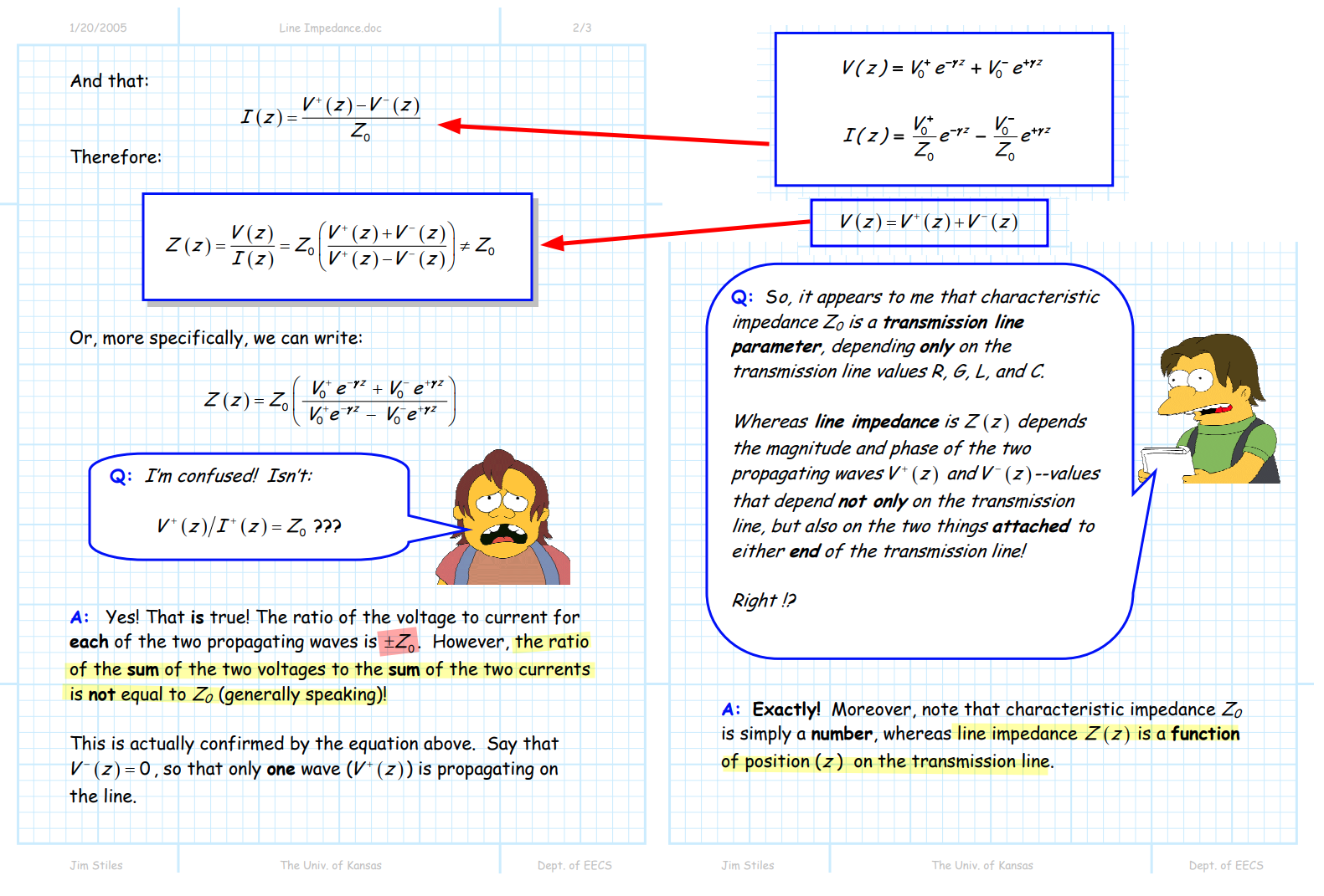
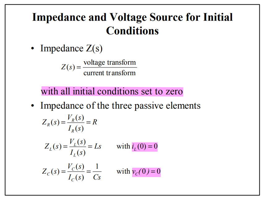
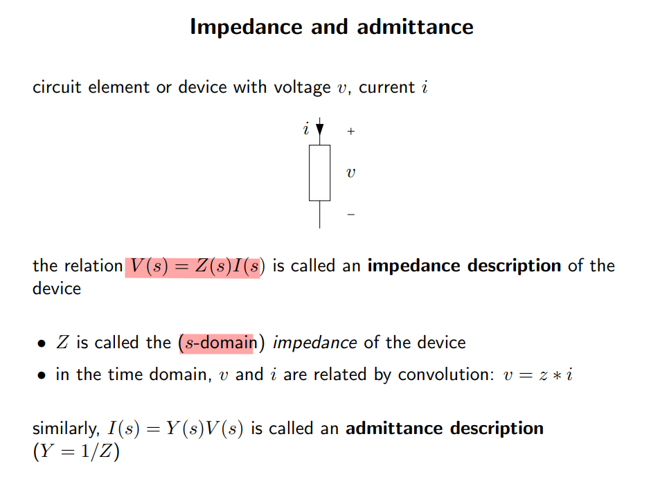
Impedance and Admittance

Impedance and admittance are generalizations of resistance and conductance.

They differ from resistance and conductance in that they are complex and they vary with frequency.

Impedance is defined to be the ratio of the phasor for the voltage across the component and the current through the component: \[ Z = \frac{V}{I} \]

Impedance is a complex value. The real part of the impedance is referred to as the resistance and the imaginary part is referred to as the reactance

For a linear component, admittance is defined to be the ratio of the phasor for the current through the component and the voltage across the component: \[ Y = \frac{I}{V} \]

Admittance is a complex value. The real part of the admittance is referred to as the conductance and the imaginary part is referred to as the susceptance.

Response to Complex Exponentials

The response of an LTI system to a complex exponential input is the same complex exponential with only a change in amplitude

\[\begin{align} y(t) &= H(s)e^{st} \\ H(s) &= \int_{-\infty}^{+\infty}h(\tau)e^{-s\tau}d\tau \end{align}\]

where \(h(t)\) is the impulse response of a continuous-time LTI system

convolution integral is used here

\[\begin{align} y[n] &= H(z)z^n \\ H(z) &= \sum_{k=-\infty}^{+\infty}h[k]z^{-k} \end{align}\]

where \(h(n)\) is the impulse response of a discrete-time LTI system

convolution sum is used here

The signals of the form \(e^{st}\) in continuous time and \(z^{n}\) in discrete time, where \(s\) and \(z\) are complex numbers are referred to as an eigenfunction of the system, and the amplitude factor \(H(s)\), \(H(z)\) is referred to as the system's eigenvalue

Laplace transform

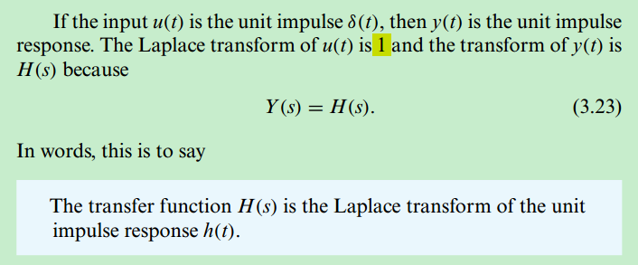
One of the important applications of the Laplace transform is in the analysis and characterization of LTI systems, which stems directly from the convolution property \[ Y(s) = H(s)X(s) \] where \(X(s)\), \(Y(s)\), and \(H(s)\) are the Laplace transforms of the input, output, and impulse response of the system, respectively

From the response of LTI systems to complex exponentials, if the input to an LTI system is \(x(t) = e^{st}\), with \(s\) the ROC of \(H(s)\), then the output will be \(y(t)=H(s)e^{st}\); i.e., \(e^{st}\) is an eigenfunction of the system with eigenvalue equal to the Laplace transform of the impulse response.

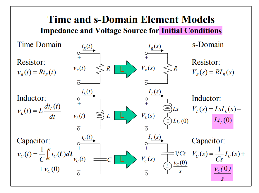
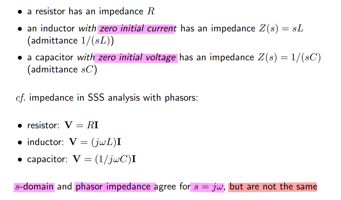
s-Domain Element Models

image-20231223225541693

image-20231223225609893

Sinusoidal Steady-State Analysis

Here Sinusoidal means that source excitations have the form \(V_s\cos(\omega t +\theta)\) or \(V_s\sin(\omega t+\theta)\)

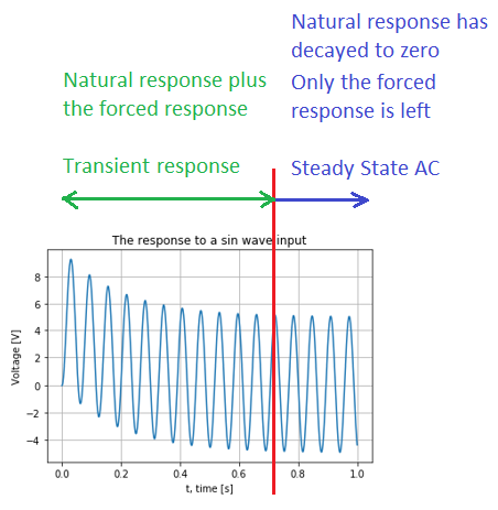
Steady state mean that all transient behavior of the stable circuit has died out, i.e., decayed to zero

image-20231223212820547

image-20231223212846596

image-20231223213016508

\(s\)-domain and phasor-domain

Phasor analysis is a technique to find the steady-state response when the system input is a sinusoid. That is, phasor analysis is sinusoidal analysis.

  • Phasor analysis is a powerful technique with which to find the steady-state portion of the complete response.
  • Phasor analysis does not find the transient response.
  • Phasor analysis does not find the complete response.

The beauty of the phasor-domain circuit is that it is described by algebraic KVL and KCL equations with time-invariant sources, not differential equations of time

image-20231224001422189

image-20231223230739219

The difference here is that Laplace analysis can also give us the transient response

image-20231224132406755

General Response Classifications

img

  • zero-input response, zero-state response & complete response

    image-20231223235252850

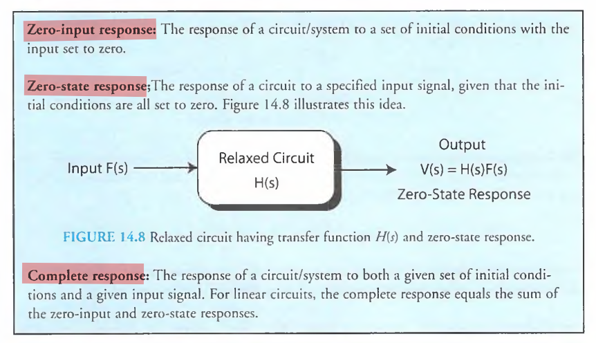
    The zero-state response is given by \(\mathscr{L^1}[H(s)F(s)]\), for the arbitrary \(s\)-domain input \(F(s)\)

    where \(Z_L(s) = sL\), the inductor with zero initial current \(i_L(0)=0\) and \(Z_C(s)=1/sC\) with zero initial voltage \(v_C(0)=0\)

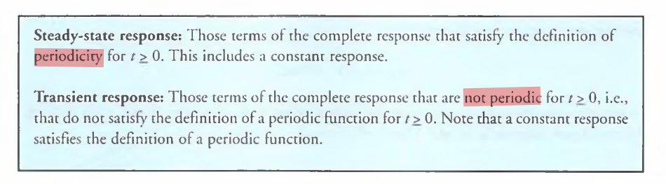
  • transient response & steady-state response

    image-20231224000454014

  • natural response & forced response

    image-20231224000817438


image-20240118212304219

Transfer Functions and Frequency Response

transfer function

The transfer function \(H(s)\) is the ratio of the Laplace transform of the output of the system to its input assuming all zero initial conditions.

image-20240106185523937

image-20240106185937270

frequency response

An immediate consequence of convolution is that an input of the form \(e^{st}\) results in an output \[ y(t) = H(s)e^{st} \] where the specific constant \(s\) may be complex, expressed as \(s = \sigma + j\omega\)

A very common way to use the exponential response of LTIs is in finding the frequency response i.e. response to a sinusoid

First, we express the sinusoid as a sum of two exponential expressions (Euler’s relation): \[ \cos(\omega t) = \frac{1}{2}(e^{j\omega t}+e^{-j\omega t}) \] If we let \(s=j\omega\), then \(H(-j\omega)=H^*(j\omega)\), in polar form \(H(j\omega)=Me^{j\phi}\) and \(H(-j\omega)=Me^{-j\phi}\). \[\begin{align} y_+(t) & = H(s)e^{st}|_{s=j\omega} = H(j\omega)e^{j\omega t} = M e^{j(\omega t + \phi)} \\ y_-(t) & = H(s)e^{st}|_{s=-j\omega} = H(-j\omega)e^{-j\omega t} = M e^{-j(\omega t + \phi)} \end{align}\]

By superposition, the response to the sum of these two exponentials, which make up the cosine signal, is the sum of the responses \[\begin{align} y(t) &= \frac{1}{2}[H(j\omega)e^{j\omega t} + H(-j\omega)e^{-j\omega t}] \\ &= \frac{M}{2}[e^{j(\omega t + \phi)} + e^{-j(\omega t + \phi)}] \\ &= M\cos(\omega t + \phi) \end{align}\]

where \(M = |H(j\omega|\) and \(\phi = \angle H(j\omega)\)

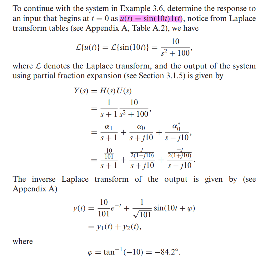
This means if a system represented by the transfer function \(H(s)\) has a sinusoidal input, the output will be sinusoidal at the same frequency with magnitude \(M\) and will be shifted in phase by the angle \(\phi\)

Laplace transform vs. Fourier transform

  • Laplace transforms such as \(Y(s)=H(s)U(s)\) can be used to study the complete response characteristics of systems, including the transient response—that is, the time response to an initial condition or suddenly applied signal
  • This is in contrast to the use of Fourier transforms, which only take into account the steady-state response

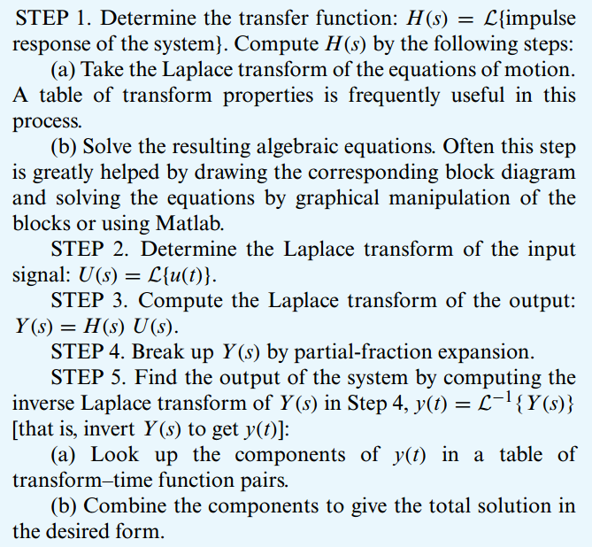
Given a general linear system with transfer function \(H(s)\) and an input signal \(u(t)\), the procedure for determining \(y(t)\) using the Laplace transform is given by the following steps:

image-20240106224403401

Laplace derivative formula at \(t = 0\)

S. Boyd EE102 Table of Laplace Transforms. [https://web.stanford.edu/~boyd/ee102/laplace-table.pdf]

One-Sided (unilateral) and Two-Sided (bilateral) Laplace Transforms

[https://sps.ewi.tudelft.nl/Education/courses/ee2s11/slides/3_laplace_P.pdf]

reference

Ken Kundert. Introduction to Phasors. Designer’s Guide Community. September 2011.

How to Perform Linearity Circuit Analysis [https://resources.pcb.cadence.com/blog/2021-how-to-perform-linearity-circuit-analysis]

Stephen P. Boyd. EE102 Lecture 7 Circuit analysis via Laplace transform [https://web.stanford.edu/~boyd/ee102/laplace_ckts.pdf]

Cheng-Kok Koh, EE695K VLSI Interconnect, S-Domain Analysis [https://engineering.purdue.edu/~chengkok/ee695K/lec3c.pdf]

Kenneth R. Demarest, Circuit Analysis using Phasors, Laplace Transforms, and Network Functions [https://people.eecs.ku.edu/~demarest/212/Phasor%20and%20Laplace%20review.pdf]

DeCarlo, R. A., & Lin, P.-M. (2009). Linear circuit analysis : time domain, phasor, and Laplace transform approaches (3rd ed).

Davis, Artice M.. "Linear Circuit Analysis." The Electrical Engineering Handbook - Six Volume Set (1998)

Duane Marcy, Fundamentals of Linear Systems [http://lcs-vc-marcy.syr.edu:8080/Chapter22.html]

Gene F. Franklin, J. David Powell, and Abbas Emami-Naeini. 2018. Feedback Control of Dynamic Systems (8th Edition) (8th. ed.). Pearson.

Data Register, DR:

  • Bypass Register, BR
  • Boundary Scan Register, BSR

Instruction Register, IR

TAP Controller

image-20240113191225838

  • FSM and Shift Register of DR and IR works at the posedge of the clock
  • TMS, TDI, TDO and Hold Register of DR and IR changes value at the negedge of the clock

image-20240113191409296

image-20240113191526490

capture IR 01, the fixed is for easier fault detection

image-20231129232443249

image-20231129233218011

After power-up, they may not be in sync, but there is a trick. Look at the state machine and notice that no matter what state you are, if TMS stays at "1" for five clocks, a TAP controller goes back to the state "Test-Logic Reset". That's used to synchronize the TAP controllers.

It is important to note that in a typical Boundary-Scan test, the time between launching a signal from driver (at the falling edge of test clock (TCK) in the Update-DR or Update-IR TAP Controller state) and capturing that signal (at the rising edge of TCK in the Caputre-DR TAP Controller state) is no less tha 2.5 TCK cycles

Further, the time between successive launches on a driver is governed - not only by the TCk rate - but by the amount of serial data shifting needed to load the next pattern data in the concatenated Boundary-Scan Registers of the Boundary-Scan chain

Thus the effective test data rate of a driver could be thousands of the times lower than the TCK rate

  1. For DC-coupled interconnect, this time is of no concern
  2. For AC-coupled interconnect, the signal may easily decay partially or completely before it can be captured
  3. If only partial decay occurs before capture, that decay will very likely be completed before the driver produces the next edge

AC-coupling

In general, AC-coupling can distort a signal transmitted across a channel depending on its frequency.

Figure 5

  • The high frequency signal is relatively unaffected by the coupling
  • The low frequency signal is severely impacted
    1. it decays to \(V_T\) after a few time constants
    2. its amplitude is double the input amplitude > transient response, before AC-coupling capacitor: \(-A_p \to A_p\); after AC-coupling capacitor \(V_T \to V_T+2A_p\) > A key item to note is that the transitions in the original signal are preserved, although their start and end points are offset > > compared to where they were in the high frequency

Test signal implementation

The test data is either the content of the Boundary-Scan Register Update latch (U) when executing the (DC) EXTEST instruction, or an "AC Signal" when an AC testing instruction is loaded into the device.

The AC signal is a test waveform suited for transmission through AC-coupling

image-20240113184502597

Test signal reception

  • When an AC testing instruction is loaded, a specialized test receiver detects transitoins of the AC signal seen at the input and determines if this represents a logic '0' or '1'
  • When EXTEST is loaded, the input signal level is detected and sent to the output of the test receiver to the Boundary-Scan Register cell

When testing for a shorted capacitor, the test software must ensure that enough time has passed for the signal to decay before entering Capture-DR, either by stopping TCk or by spending additional TCK cycles in the Run-Test/Idle TAP Controller state

EXTEST_PULSE & EXTEST_TRAIN

The two new AC-test instructions provided by this standard differ primarily in the number and timing of transitions to provide flexibility in dealing with the specific dynamic behavior of the channels being tested

AC Test Signal essentially modulates test data so that it will propagate through AC-coupled channels, for devices that contatin AC pins

Tools should use the EXTEST_PULSE instruction unless there is a specific requirement for the EXTEST_TRAIN instruction

EXTEST_PULSE

Generate two additional driver transitions and allows a tester to vary the time between them dependent on how many TCK cycles the TAP is left in the Run-Test/Idle TAP Controller state.

This is intended to allow any undesired transient condition to decay to a DC steady-state value when that will make the final transition more reliably detectable

The duration in the Run-Test/Idle TAP Controller state should be at least three times the high-pass coupling time constant. This allows the first additional transition to decay away to the DC steady-state value for the channel, and ensures that the full amplitude of the final transition is added to or subtracted from that steady-state value

This establishes a known initial condition for the final transition and permits reliable specification of the detection threshold of the test receiver

image-20240113190314947

EXTEST_TRAIN

Generate multiple additional transitions, the number dependent on how long the TAP is left in the Run-Test/Idle TAP Controller state

This is intended to allow any undesired transient condition to decay to an AC steady-state value when that will make the final transition more reliably detectable

image-20240113190345323

IEEE Std 1149.6-2003

This standard is built on top of IEEE Std 1149.1 using the same Test Access Port structure and Boundary-Scan architecture.

  • It adds the concept of a "test receiver" to input pins that are expected to handle differential and/or AC-coupling
  • It adds two new instructions that cause drivers to emit AC waveforms that are processed by test receivers.

JTAG Instruction

Implementation

  • AC mode hysteresis, detect transistion
  • DC mode threshold is determined by jtag initial value

reference

IEEE Std 1149.1-2001, IEEE Standard Test Access Port and Boundary-Scan Architecture, IEEE, 2001

IEEE Std 1149.6-2003, IEEE Standard for BoundaryScan Testing of Advanced Digital Networks, IEEE, 2003

IEEE 1149.6 Tutorial | Testing AC-coupled and Differential High-speed Nets [https://www.asset-intertech.com/resources/eresources/ieee-11496-tutorial-testing-ac-coupled-and-differential-high-speed-nets/]

Prof. James Chien-Mo Li, Lab of Dependable Systems, National Taiwan University. VLSI Testing [http://cc.ee.ntu.edu.tw/~cmli/VLSItesting/]

K.P. Parker, The Boundary Scan Handbook, 3rd ed., Kluwer Academic, 2003.

B. Eklow, K. P. Parker and C. F. Barnhart, "IEEE 1149.6: a boundary-scan standard for advanced digital networks," in IEEE Design & Test of Computers, vol. 20, no. 5, pp. 76-83, Sept.-Oct. 2003, doi: 10.1109/MDT.2003.1232259.

image-20241106231114717


autocorrelation

image-20241116112504606

The expectation returns the probability-weighted average of the specific function at that specific time over all possible realizations of the process


Derivatives of Random Processes

since \(x(t)\) is stationary process, and \(y(t) = \frac{\mathrm{d}x(t)}{\mathrm{d}t}\)

Using \(R_{yy}(\tau) = h(\tau)*R_{xx}(\tau)*h(-\tau)\)

\[\begin{align} R_{yy}(\tau) &= \mathcal{F}^{-1}[H(j\omega)\Phi_{xx}(j\omega)H(-j\omega)] \\ &= \mathcal{F}^{-1}[-(j\omega)^2\Phi_{xx}(j\omega)] \end{align}\]

we obtain the autocorrelation function of the output process as \[ R_{yy}(\tau) = -\frac{\mathrm{d}^2}{\mathrm{d}\tau^2}R_{xx}(\tau) \]

Liu Congfeng, Xidian University. Random Signal Processing: Chapter 5 Linear System: Random Process [https://web.xidian.edu.cn/cfliu/files/20121125_153218.pdf]

[https://sharif.ir/~bahram/sp4cl/PapoulisLectureSlides/lectr14.pdf]

Ergodicity

ensemble autocorrelation and temporal autocorrelation (time autocorrelation)

image-20240719230346944

image-20240719210621021


image-20241123004051314


ECE438 - Laboratory 7: Discrete-Time Random Processes (Week 2) October 6, 2010 [https://engineering.purdue.edu/VISE/ee438L/lab7/pdf/lab7b.pdf]

Ensemble Averages & Time Averages

[https://ece-research.unm.edu/bsanthan/ece541/stat.pdf]

[https://www.nii.ac.jp/qis/first-quantum/e/forStudents/lecture/pdf/noise/chapter1.pdf]

  • time average: time-averaged quantities for the \(i\)-th member of the ensemble
  • ensemble average: ensemble-averaged quantities for all members of the ensemble at a certain time

image-20241116113758119

image-20260305230152167

image-20241116215119239

image-20241116215140298

where \(\theta\) is one member of the ensemble; \(p(x)dx\) is the probability that \(x\) is found among \([x, x + dx]\)

sample autocorrelation

[https://engineering.purdue.edu/VISE/ee438L/lab7/pdf/lab7b.pdf]

image-20250912203526260


[http://www.signal.uu.se/Courses/CourseDirs/SignalbehandlingIT/forelas02.pdf]

image-20250912205534933

ergodic vs. stationary

[https://bookdown.org/kevin_davisross/stat350-handouts/stationary.html]

image-20250912211619068


image-20250912211353183

Strict Sense Stationary (SSS) & Wide Sense Stationary (WSS)

[https://ece-research.unm.edu/bsanthan/ece541/station.pdf]

image-20250912210738010


image-20241123221623537

image-20240720140527704


mean

image-20240917104857284

image-20240917104916086

Wiener-Khinchin theorem

Norbert Wiener proved this theorem for the case of a deterministic function in 1930; Aleksandr Khinchin later formulated an analogous result for stationary stochastic processes and published that probabilistic analogue in 1934. Albert Einstein explained, without proofs, the idea in a brief two-page memo in 1914

Continuous time

[https://www.robots.ox.ac.uk/~dwm/Courses/2TF_2011/2TF-L5.pdf]

Frank R. Kschischang. The Wiener-Khinchin Theorem [https://www.comm.utoronto.ca/~frank/notes/wk.pdf]

image-20240910003805151

\(x(t)\), Fourier transform over a limited period of time \([-T/2, +T/2]\) , \(X_T(f) = \int_{-T/2}^{T/2}x(t)e^{-j2\pi ft}dt\)

With Parseval's theorem \[ \int_{-T/2}^{T/2}|x(t)|^2dt = \int_{-\infty}^{\infty}|X_T(f)|^2df \] So that \[ \frac{1}{T}\int_{-T/2}^{T/2}|x(t)|^2dt = \int_{-\infty}^{\infty}\frac{1}{T}|X_T(f)|^2df \]

where the quantity, \(\frac{1}{T}|X_T(f)|^2\) can be interpreted as distribution of power in the frequency domain

For each \(f\) this quantity is a random variable, since it is a function of the random process \(x(t)\)

The power spectral density (PSD) \(S_x(f )\) is defined as the limit of the expectation of the expression above, for large \(T\): \[ S_x(f) = \lim _{T\to \infty}\mathrm{E}\left[ \frac{1}{T}|X_T(f)|^2 \right] \]

The Wiener-Khinchin theorem ensures that for well-behaved wide-sense stationary processes the limit exists and is equal to the Fourier transform of the autocorrelation \[\begin{align} S_x(f) &= \int_{-\infty}^{+\infty}R_x(\tau)e^{-j2\pi f \tau}d\tau \\ R_x(\tau) &= \int_{-\infty}^{+\infty}S_x(f)e^{j2\pi f \tau}df \end{align}\]

Note: \(S_x(f)\) in Hz and inverse Fourier Transform in Hz (\(\frac{1}{2\pi}d\omega = df\))

Topic 6 Random Processes and Signals [https://www.robots.ox.ac.uk/~dwm/Courses/2TF_2021/N6.pdf]

image-20260304223136726


Example

image-20240904203802604

Remember: impulse scaling

image-20240718210137344 \[ \cos(2\pi f_0t) \overset{\mathcal{F}}{\longrightarrow} \frac{1}{2}[\delta(f -f_0)+\delta(f+f_0)] \]


image-20250821200319537


\(x(t)\) \(R(\tau)\)
\(A_0 \sin(\omega_0 t+\phi_0)\) \(\frac{A_0^2}{2}\cos(\omega_0 \tau)\)
\(A_0 \cos(\omega_0 t+\phi_0)\) \(\frac{A_0^2}{2}\cos(\omega_0 \tau)\)

due to \(\cos(\omega_0 t +\phi_0) = \sin(\omega_0 t +\phi_0 + \frac{\pi}{2})\)

Discrete time

Diniz PSR, da Silva EAB, Netto SL. Digital Signal Processing: System Analysis and Design. 2nd ed. Cambridge University Press; 2010.

image-20260304232947364

filtered by a linear time-invariant systemimage-20260304233139451


ACF of discrete-time sinusoid. Google AI Mode [https://share.google/aimode/IHyr7o8jLUMx2Leb3]

image-20260305224358226

image-20260305224328950


SIMG-713 Noise and Random Processes Spring 2002 . Lecture 15 Power Spectrum Estimation [https://www.cis.rit.edu/class/simg713/Lectures/Lecture713-15-4.pdf]

Properties of the Fourier Transform for Discrete-Time Signals [https://www.comm.utoronto.ca/dkundur/course_info/362/EmanHammadDTFT2.pdf]

image-20260304231554434 \[ \frac{1}{2\pi}F^{-1}\{R_{xx}\}d\omega = \frac{1}{2\pi}F^{-1}\{R_{xx}\}d(2\pi f T)=T\cdot F^{-1}\{R_{xx}\}df = P_{xx}(f)df \] power spectral density of a discrete-time random process \(\{x(n)\}\) is given by \[ P_{xx}(f) =T\cdot F^{-1}\{R_{xx}\} \]

PSD & ESD

David Murray. Topic 5 Energy & Power Spectra, and Correlation [https://www.robots.ox.ac.uk/~dwm/Courses/2TF_2011/2TF-L5.pdf]

Finite Energy signals & Finite Power signals

image-20260305231350101


image-20260305225312430

image-20260305230629208

image-20260305231618933


2.161 Signal Processing - Continuous and Discrete Fall Term 2008 Lecture 22 [pdf]

image-20260305232711337


Sklar, Bernard. Digital communications: fundamentals and applications. Pearson, 2021.

image-20260308111211454

LTI Filtering of WSS process

image-20240827221945277

CT Deterministic Autocorrelation Function

Topic 6 Random Processes and Signals [https://www.robots.ox.ac.uk/~dwm/Courses/2TF_2021/N6.pdf]

Alan V. Oppenheim, Introduction To Communication, Control, And Signal Processing [https://ocw.mit.edu/courses/6-011-introduction-to-communication-control-and-signal-processing-spring-2010/a6bddaee5966f6e73450e6fe79ab0566_MIT6_011S10_notes.pdf]

Balu Santhanam, Probability Theory & Stochastic Process 2020: LTI Systems and Random Signals [https://ece-research.unm.edu/bsanthan/ece541/LTI.pdf]

image-20260305211727250 \[ R_{yy}(\tau) = h(\tau)*R_{xx}(\tau)*h(-\tau) =R_{xx}(\tau)*h(\tau)*h(-\tau) \]

image-20240907211343832

why \(\overline{R}_{hh}(\tau) \overset{\Delta}{=} h(\tau)*h(-\tau)\) is autocorrelation ? the proof is as follows:

\[\begin{align} \overline{R}_{hh}(\tau) &= h(\tau)*h(-\tau) \\ &= \int_{-\infty}^{\infty}h(x)h(-(\tau - x))dx \\ &= \int_{-\infty}^{\infty}h(x)h(-\tau + x)dx \\ &=\int_{-\infty}^{\infty}h(x+\tau)h(x)dx \end{align}\]


image-20240827222224395

image-20240827222235906


Time Reversal \[ x(-t) \overset{FT}{\longrightarrow} X(-j\omega) \]

if \(x(t)\) is real, then \(X(j\omega)\)​ has conjugate symmetry \[ X(-j\omega) = X^*(j\omega) \]

DT Deterministic Autocorrelation Function

image-20260305222010513

image-20260305222059412

\[ c_{hh}[l] = \sum_{k=-\infty}^{\infty}h[k]h[l+k]=\sum_{k=-\infty}^{\infty}h[-l+k]h[k]=\sum_{k=-\infty}^{\infty}h[-(l-k)]h[k]=h[l]*h[-l] \] image-20260305223209840

Periodogram

The periodogram is in fact the Fourier transform of the aperiodic correlation of the windowed data sequence

image-20240907215822425

image-20240907215957865

image-20240907230715637


estimating continuous-time stationary random signal

periodogram.drawio

The sequence \(x[n]\) is typically multiplied by a finite-duration window \(w[n]\), since the input to the DFT must be of finite duration. This produces the finite-length sequence \(v[n] = w[n]x[n]\)

image-20240910005608007

image-20240910005927534

image-20240910005723458

\[\begin{align} \hat{P}_{ss}(\Omega) &= \frac{|V(e^{j\omega})|^2}{LU} \\ &= \frac{|V(e^{j\omega})|^2}{\sum_{n=0}^{L-1}(w[n])^2} \tag{1}\\ &= \frac{L|V(e^{j\omega})|^2}{\sum_{k=0}^{L-1}(W[k])^2} \tag{2} \end{align}\]

image-20240910010638376

That is, by \((1)\) \[ \hat{P}_{ss}(\Omega) = T_s\hat{P}_{xx(\omega)} = \frac{T_s|V(e^{j\omega})|^2}{\sum_{n=0}^{L-1}(w[n])^2}=\frac{|V(e^{j\omega})|^2}{f_{res}L\sum_{n=0}^{L-1}(w[n])^2} \]

That is, by \((2)\) \[ \hat{P}_{ss}(\Omega) = T_s\hat{P}_{xx(\omega)} = \frac{T_sL|V(e^{j\omega})|^2}{\sum_{k=0}^{L-1}(W[k])^2} = \frac{|V(e^{j\omega})|^2}{f_{res}\sum_{k=0}^{L-1}(W[k])^2} \]

!! ENBW

Periodic & Cyclostationary Processes

image-20250809234136591

image-20250809234318422

Multirate Systems & Random Sequences

Balu Santhanam. ece541 Probability Theory & Stochastic Process: Random Signals and Multirate Systems [http://ece-research.unm.edu/bsanthan/ece541/rand.pdf]

WSS Random Sequences

autocorrelation function of WSS random sequences

image-20250818202413226


psd of WSS of WSS random sequences

image-20250818202138087


Interpretation of the psd

image-20250818205138125

Equation 8.4-4 is permissible for cyclostationary waveforms

decimation

image-20250810194206762

\[ \frac{1}{M}\int_{-Mx_0}^{Mx_0}f(\frac{x}{M})dx = \int_{-Mx_0}^{Mx_0}f(\frac{x}{M}) d\frac{x}{M} = \int_{-x_0}^{x_0} f(\acute{x}) d\acute{x} \]

where \(\acute{x} = \frac{x}{M}\)

randSeq-decimation.drawio


image-20250818195951584

image-20250818205826429

interpolation

image-20250819182525306

The resulting expanded random sequence is clearly nonstationary, because of the zero insertions.

image-20250810194541608

This random sequences and processes is classified as being cyclostationary

psd of \(X_e[n]\), the expansion or the upsampled version of \(X[n]\)

\[ S_{X_eX_e}(\omega) = \frac{1}{L}S_{XX}(L\omega) \]

where \(L\) is upsampling factor

image-20250810204047368

apply \(X_e[n]\) to an ideal lowpass filter with bandwidth \([-\pi/2 , +\pi/2]\) and gain of \(2\) or \(L\)

\[ S_{YY}(\omega) = \left\{ \begin{array}{cl} L \cdot S_{XX}(L\omega), &\ |\omega|\leq \pi/L \\ 0, &\ \pi/L \lt |\omega| \leq \pi \end{array} \right. \]


Stark H, Woods JW. Probability, Statistics, and Random Processes for Engineers, 3rd [pdf]

—, 3th Ed Solution Manual [https://www.scribd.com/document/353335818/Stark-Woods-3th-Ed-Manual#page=212]

image-20250818222910938

General case with upsampling factor \(L\)

\[\begin{align} &\mathrm{E}\{|\sum_{n=-N}^N X_e[n]e^{-j\omega n}|^2\}\\ &= \sum_{n=-N}^N\sum_{l=-N}^NX_e[n]\cdot X_e^*[l]\cdot e^{-j\omega(n-l)}\\ &= \sum_{n=-N}^N\sum_{l=-N}^NX[\frac{n}{L}]\cdot X^*[\frac{l}{L}]\cdot e^{-j\omega(n-l)}\\ &= \sum_{k=-N/L}^{N/L}\sum_{m=-N/L}^{N/L}X[k]\cdot X^*[m]\cdot e^{-jL\omega (k-m)}\\ &= \sum_{k=-\infty}^{\infty}\sum_{m=-\infty}^{\infty}R_{XX}[k-m]\cdot e^{-j\omega L(k-m)}\cdot \mathcal{rect}[\frac{k}{2N/L}]\cdot \mathcal{rect}[\frac{m}{2N/L}]\\ &= \sum_{i=-\infty}^{\infty}\sum_{m=-\infty}^{\infty}R_{XX}[i]\cdot e^{-jL\omega i}\cdot \mathcal{rect}[\frac{i+m}{2N/L}]\cdot \mathcal{rect}[\frac{m}{2N/L}]\\ &= \sum_{i=-\infty}^{\infty}R_{XX}[i]\cdot e^{-jL\omega i} \cdot \frac{2N}{L}\left[1 -\frac{|i|}{2N/L} \right] \end{align}\]

Then \[\begin{align} S_{X_eX_e}(\omega) &= \lim_{N\to \infty}\frac{1}{2N+1}\cdot \mathrm{E}\{|\sum_{n=-N}^N X_e[n]e^{-j\omega n}|^2\} \\ &= \frac{1}{L}\sum_{i=-\infty}^{\infty}R_{XX}[i]\cdot e^{-jL\omega i}\\ &= \frac{1}{L}S_{XX}(L\omega) \end{align}\]


image-20250818211010290

image-20250818205936474

Wiener Process (Brownian Motion)

Dennis Sun, Introduction to Probability: Lesson 49 Brownian Motion [https://dlsun.github.io/probability/brownian-motion.html]

Wiener process (also called Brownian motion)

unnamed-chunk-178-1

image-20241202001449997

NRZ PSD

Lecture 26 Autocorrelation Functions of Random Binary Processes [https://bpb-us-e1.wpmucdn.com/sites.gatech.edu/dist/a/578/files/2003/12/ECE3075A-26.pdf]

Lecture 32 Correlation Functions & Power Density Spectrum, Cross-spectral Density [https://bpb-us-e1.wpmucdn.com/sites.gatech.edu/dist/a/578/files/2003/12/ECE3075A-32.pdf]

image-20231111100420675

image-20231111101322771

image-20260301000540854

note \(\color{red}S_x(0)=0\)


Normal Distribution and Input-Referred Noise [https://a2d2ic.wordpress.com/2013/06/05/normal-distribution-and-input-referred-noise/]

Fig.1 PDF for sum of a large number of random variables

Fig.2 The noise signal, its auto correlation function, and spectral density [2]

reference

L.W. Couch, Digital and Analog Communication Systems, 8th Edition, 2013 [pdf]

Alan V Oppenheim, George C. Verghese, Signals, Systems and Inference, 1st edition [pdf]

R. Ziemer and W. Tranter, Principles of Communications, Seventh Edition, 2013 [pdf]

Stark H, Woods JW. Probability, Statistics, and Random Processes for Engineers, 4th ed. 2012 [pdf]

Kuchler, Ryan J. Theory of multirate statistical signal processing and applications. Monterey, California.: Naval Postgraduate School, 2005. [pdf]


Balu Santhanam. Fall 2020 ECE541 Probability Theory & Stochastic Process [https://ece-research.unm.edu/bsanthan/ece541/]

PSS and HB Overview

The steady-state response is the response that results after any transient effects have dissipated.

The large signal solution is the starting point for small-signal analyses, including periodic AC, periodic transfer function, periodic noise, periodic stability, and periodic scattering parameter analyses.

Designers refer periodic steady state analysis in time domain as "PSS" and corresponding frequency domain notation as "HB"

image-20231028163033255

Harmonic Balance Analysis

The idea of harmonic balance is to find a set of port voltage waveforms (or, alternatively, the harmonic voltage components) that give the same currents in both the linear-network equations and nonlinear-network equations

that is, the currents satisfy Kirchoff's current law

Define an error function at each harmonic, \(f_k\), where \[ f_k = I_{\text{LIN}}(k\omega) + I_{\text{NL}}(k\omega) \] where \(k=0, 1, 2,...,K\)

Note that each \(f_k\) is implicitly a function of all voltage components \(V(k\omega)\)

Newton Solution of the Harmonic-Balance Equation

Iterative Process and Jacobian Formulation

image-20231108222451147

The elements of the Jacobian are the derivatives \[ \frac{\partial F_{\text{n,k}}}{\partial _{V_\text{m,l}}} \] where \(n\) and \(m\) are the port indices \((1,N)\), and \(k\) and \(l\) are the harmonic indices \((0,...,K)\)

Number of Harmonics & Time Samples

image-20251013203212011


image-20251014065943176

Initial Estimate

One important property of Newton's method is that its speed and reliability of convergence depend strongly upon the initial estimate of the solution vector.

Conversion Matrix Analysis

Large-signal/small-signal analysis, or conversion matrix analysis, is useful for a large class of problems wherein a nonlinear device is driven, or "pumped" by a single large sinusoidal signal; another signal, much smaller, is applied; and we seek only the linear response to the small signal.

The most common application of this technique is in the design of mixers and in nonlinear noise analysis

  1. First, analyzing the nonlinear device under large-signal excitation only, where the harmonic-balance method can be applied
  2. Then, the nonlinear elements in the device's equivalent circuit are then linearized to create small-signal, linear, time-varying elements
  3. Finally, a small-signal analysis is performed

Element Linearized

Below shows a nonlinear resistive element, which has the \(I/V\) relationship \(I=f(V)\). It is driven by a large-signal voltage

image-20220511203515431

Assuming that \(V\) consists of the sum of a large-signal component \(V_0\) and a small-signal component \(v\), with Taylor series \[ f(V_0+v) = f(V_0)+\frac{\mathrm{d}}{\mathrm{d}V}f(V)|_{V=V_0}\cdot v+\frac{1}{2}\frac{\mathrm{d}^2}{\mathrm{d}V^2}f(V)|_{V=V_0}\cdot v^2+... \] The small-signal, incremental current is found by subtracting the large-signal component of the current \[ i(v)=I(V_0+v)-I(V_0) \] If \(v \ll V_0\), \(v^2\), \(v^3\),... are negligible. Then, \[ i(v) = \frac{\mathrm{d}}{\mathrm{d}V}f(V)|_{V=V_0}\cdot v \]

\(V_0\) need not be a DC quantity; it can be a time-varying large-signal voltage \(V_L(t)\) and that \(v=v(t)\), a function of time. Then \[ i(t)=g(t)v(t) \] where \(g(t)=\frac{\mathrm{d}}{\mathrm{d}V}f(V)|_{V=V_L(t)}\)

The time-varying conductance \(g(t)\), is the derivative of the element's \(I/V\) characteristic at the large-signal voltage

By an analogous derivation, one could have a current-controlled resistor with the \(V/I\) characteristic \(V = f_R(I)\) and obtain the small-signal \(v/i\) relation \[ v(t) = r(t)i(t) \] where \(r(t) = \frac{\mathrm{d}}{\mathrm{d}I}f_R(I)|_{I=I_L(t)}\)

A nonlinear element excited by two tones supports currents and voltages at mixing frequencies \(m\omega_1+n\omega_2\), where \(m\) and \(n\) are integers. If one of those tones, \(\omega_1\) has such a low level that it does not generate harmonics and the other is a large-signal sinusoid at \(\omega_p\), then the mixing frequencies are \(\omega=\pm\omega_1+n\omega_p\), which shown in below figure

image-20231108223600922

A more compact representation of the mixing frequencies is \[ \omega_n=\omega_0+n\omega_p \] which includes only half of the mixing frequencies:

  • the negative components of the lower sidebands (LSB)
  • and the positive components of the upper sidebands (USB)

image-20220511211336437

For real signal, positive- and negative-frequency components are complex conjugate pairs

Shooting Newton

TODO 📅

Nonlinearity & Linear Time-Varying Nature

Nonlinearity Nature

The nonlinearity causes the signal to be replicated at multiples of the carrier, an effect referred to as harmonic distortion, and adds a skirt to the signal that increases its bandwidth, an effect referred to as intermodulation distortion

image-20231029093504162

It is possible to eliminate the effect of harmonic distortion with a bandpass filter, however the frequency of the intermodulation distortion products overlaps the frequency of the desired signal, and so cannot be completely removed with filtering.

Time-Varying Linear Nature

image-20231029101042671

linear with respect to \(v_{in}\) and time-varying

Given \(v_{in}(t)=m(t)\cos (\omega_c t)\) and LO signal of \(\cos(\omega_{LO} t)\), then \[ v_{out}(t) = \text{LPF}\{m(t)\cos(\omega_c t)\cdot \cos(\omega_{LO} t)\} \] and \[ v_{out}(t) = m(t)\cos((\omega_c - \omega_{LO})t) \]

A linear periodically-varying transfer function implements frequency translation

Linear Time Varying

The response of a relaxed LTV system at a time \(t\) due to an impulse applied at a time \(t − \tau\) is denoted by \(h(t, \tau)\)

The first argument in the impulse response denotes the time of observation.

The second argument indicates that the system was excited by an impulse launched at a time \(\tau\) prior to the time of observation.

Thus, the response of an LTV system not only depends on how long before the observation time it was excited by the impulse but also on the observation instant.

The output \(y(t)\) of an initially relaxed LTV system with impulse response \(h(t, \tau)\) is given by the convolution integral \[ y(t) = \int_0^{\infty}h(t,\tau)x(t-\tau)d\tau \] Assuming \(x(t) = e^{j2\pi f t}\) \[ y(t) = \int_0^{\infty}h(t,\tau)e^{j2\pi f (t-\tau)}d\tau = e^{j2\pi f t}\int_0^{\infty}h(t,\tau)e^{-j2\pi f\tau}d\tau \] The (time-varying) frequency response can be interpreted as \[ H(j2\pi f, t) = \int_0^{\infty}h(t,\tau)e^{-j2\pi f\tau}d\tau \] Linear Periodically Time-Varying (LPTV) Systems, which is a special case of an LTV system whose impulse response satisfies \[ h(t, \tau) = h(t+T_s, \tau) \] In other words, the response to an impulse remains unchanged if the time at which the output is observed (\(t\)) and the time at which the impulse is applied (denoted by \(t_1\)) are both shifted by \(T_s\) \[ H(j2\pi f, t+T_s) = \int_0^{\infty}h(t+T_s,\tau)e^{-j2\pi f\tau}d\tau = \int_0^{\infty}h(t,\tau)e^{-j2\pi f\tau}d\tau = H(j2\pi f, t) \] \(H(j2\pi f, t)\) of an LPTV system is periodic with timeperiod \(T_s\), it can be expanded as a Fourier series in \(t\), resulting in \[ H(j2\pi f, t) = \sum_{k=-\infty}^{\infty} H_k(j2\pi f)e^{j2\pi f_s k t} \] The coefficients of the Fourier series \(H_k(j2\pi f)\) are given by \[ H_k(j2\pi f) = \frac{1}{T_s}\int_0^{T_s} H(j2\pi f, t) e^{-j2\pi k f_s t}dt \]

Periodic small signal in SpectreRF

B. Boser,A, 2011EECS 240 Topic 6: Noise Analysis [https://mixsignal.wordpress.com/wp-content/uploads/2013/06/t06noiseanalysis_simone-1.pdf]

Vishal Saxena, "SpectreRF Periodic Analysis" [https://www.eecis.udel.edu/~vsaxena/courses/ece614/Handouts/SpectreRF%20Periodic%20Analysis.pdf]

Ashwin Kumar, Lecture 8: Basics of periodic steady-state (pss), pac and pxf simulation demos in Cadence SpectreRF [https://youtu.be/I9zkt1OTWB0]

pss, pac and pxf

  1. LPV analyses start by performing a periodic analysis to compute the periodic operating point with only the large clock signal applied (the LO, the clock, the carrier, etc.).
  2. The circuit is then linearized about this time-varying operating point (expand about the periodic equilibrium point with a Taylor series and discard all but the first-order term)
  3. and the small information signal is applied. The response is calculated using linear time-varying analysis

Versions of this type of small-signal analysis exists for both harmonic balance and shooting methods

PAC is useful for predicting the output sidebands produced by a particular input signal

PXF is best at predicting the input images for a particular output

image-20241109110936909

image-20241109110958641

sampled pac

Sampled PAC (Spectre RF) Analysis - Strange results ? [https://designers-guide.org/forum/YaBB.pl?num=1590925194]

supply noise sensitivity: PSS+PAC or PSS+PXF [https://www.designers-guide.org/forum/YaBB.pl?num=1376500816]

Explanation for sampled PXF analysis [https://community.cadence.com/cadence_technology_forums/f/custom-ic-design/45055/explanation-for-sampled-pxf-analysis/1367253]

img

img

note: frequency axis is output

image-20260504151513974

image-20260504152448543


Which is the difference between "spectrum" sweep and "sideband" sweep in the PAC Direct Plot Form?[https://community.cadence.com/cadence_technology_forums/f/mixed-signal-design/56824/pac-simulation-sideband-sweep-parameter]

image-20260504195458391

sampled pxf

Cadence RAK: Deterministic Jitter Measurement using SpectreRF

image-20260504181711756

Sweeptype: relative + Relative Harmonic vs absolute — Output Frequency Sweep Range (Hz) \[ f_\text{abs} = f_\text{relative} + N_\text{relharmnum}\cdot f_\text{und} \] image-20260504181518289

note: frequency axis is input

relative + Relative Harmonic

1
2
3
4
5
pss  pss  fund=2.5G  harms=25  errpreset=conservative
+ annotate=status
pxf ( Out1 0 Out1 0 ) pxf crossingdirection=rise
+ thresholdvalue=1.65 ptvtype=sampled sweeptype=relative relharmnum=1
+ start=0 stop=1G step=10M maxsideband=1 annotate=status

Sweeptype: absolute

1
2
3
4
5
pss  pss  fund=2.5G  harms=25  errpreset=conservative
+ annotate=status
pxf ( Out1 0 Out1 0 ) pxf crossingdirection=rise
+ thresholdvalue=1.65 ptvtype=sampled sweeptype=absolute start=2.5G
+ stop=3.5G step=10M maxsideband=1 annotate=status

Frank Wiedmann, Using sampled pxf analysis to simulate deterministic jitter [https://community.cadence.com/cadence_technology_forums/f/custom-ic-design/51605/using-sampled-pxf-analysis-to-simulate-deterministic-jitter]

image-20260504182033946

image-20260504184951842

tran simulation verify higher frequency ripple introduce more jitter at output

image-20260504185521783

sampled pac result support the opinion of Frank Wiedmann — harmonic 0 (with no additional sidebands) introduce maximum output

image-20260504191658639

reference

K. S. Kundert, "Introduction to RF simulation and its application," in IEEE Journal of Solid-State Circuits, vol. 34, no. 9, pp. 1298-1319, Sept. 1999, doi: 10.1109/4.782091. [pdf]

Stephen Maas, Nonlinear Microwave and RF Circuits, Second Edition , Artech, 2003. [pdf]

Karti Mayaram. ECE 521 Fall 2016 Analog Circuit Simulation: Simulation of Radio Frequency Integrated Circuits [pdf1, pdf2]

The Value Of RF Harmonic Balance Analyses For Analog Verification: Frequency domain periodic large and small signal analyses. [https://semiengineering.com/the-value-of-rf-harmonic-balance-analyses-for-analog-verification/]

Shanthi Pavan, "Demystifying Linear Time Varying Circuits"

—, "Reciprocity and Inter-Reciprocity: A Tutorial— Part I: Linear Time-Invariant Networks," in IEEE Transactions on Circuits and Systems I: Regular Papers, vol. 70, no. 9, pp. 3413-3421, Sept. 2023, doi: 10.1109/TCSI.2023.3276700.

—, "Reciprocity and Inter-Reciprocity: A Tutorial—Part II: Linear Periodically Time-Varying Networks," in IEEE Transactions on Circuits and Systems I: Regular Papers, vol. 70, no. 9, pp. 3422-3435, Sept. 2023, doi: 10.1109/TCSI.2023.3294298.

—, "Interreciprocity in Linear Periodically Time-Varying Networks With Sampled Outputs," in IEEE Transactions on Circuits and Systems II: Express Briefs, vol. 61, no. 9, pp. 686-690, Sept. 2014, doi: 10.1109/TCSII.2014.2335393.

—. Introduction to Time - Varying Electrical Network. [https://youtube.com/playlist?list=PLyqSpQzTE6M8qllAtp9TTODxNfaoxRLp9]

—. EE5323: Advanced Electrical Networks (Jan-May. 2015) [https://www.ee.iitm.ac.in/vlsi/courses/ee5323/start]

R. S. Ashwin Kumar. EE698W: Analog circuits for signal processing [https://home.iitk.ac.in/~ashwinrs/2022_EE698W.html]

Piet Vanassche, Georges Gielen, and Willy Sansen. 2009. Systematic Modeling and Analysis of Telecom Frontends and their Building Blocks (1st. ed.). Springer Publishing Company, Incorporated.

Beffa, Federico. (2023). Weakly Nonlinear Systems. 10.1007/978-3-031-40681-2.

Wereley, Norman. (1990). Analysis and control of linear periodically time varying systems.

Hameed, S. (2017). Design and Analysis of Programmable Receiver Front-Ends Based on LPTV Circuits. UCLA. ProQuest ID: Hameed_ucla_0031D_15577. Merritt ID: ark:/13030/m5gb6zcz. Retrieved from https://escholarship.org/uc/item/51q2m7bx

Matt Allen. Introduction to Linear Time Periodic Systems. [https://youtu.be/OCOkEFDQKTI]

Fivel, Oren. "Analysis of Linear Time-Varying & Periodic Systems." arXiv preprint arXiv:2202.00498 (2022).

RF Harmonic Balance Analysis for Nonlinear Circuits [https://resources.pcb.cadence.com/blog/2019-rf-harmonic-balance-analysis-for-nonlinear-circuits]

Steer, Michael. Microwave and RF Design (Third Edition, 2019). NC State University, 2019.

Steer, Michael. Harmonic Balance Analysis of Nonlinear RF Circuits - Case Study Index: CS_AmpHB [link]

Josh Carnes,Peter Kurahashi. "Periodic Analyses of Sampled Systems" URL:https://slideplayer.com/slide/14865977/

Kundert, Ken. (2006). Simulating Switched-Capacitor Filters with SpectreRF. URL:https://designers-guide.org/analysis/sc-filters.pdf

Article (20482538) Title: Why is pnoise sampled(jitter) different than pnoise timeaverage on a driven circuit?

Article (20467468) Title: The mathematics behind choosing the upper frequency when simulating pnoise jitter on an oscillator

Andrew Beckett. "Simulating phase noise for PFD-CP". URL:https://groups.google.com/g/comp.cad.cadence/c/NPisXTElx6E/m/XjWxKbbfh2cJ

Dr. Yanghong Huang. MATH44041/64041: Applied Dynamical Systems [https://personalpages.manchester.ac.uk/staff/yanghong.huang/teaching/MATH4041/default.htm]

Jeffrey Wong. Math 563, Spring 2020 Applied computational analysis [https://services.math.duke.edu/~jtwong/math563-2020/main.html]

Jeffrey Wong. Math 353, Fall 2020 Ordinary and Partial Differential Equations [https://services.math.duke.edu/~jtwong/math353-2020/main.html]

Tip of the Week: Please explain in more practical (less theoretical) terms the concept of "oscillator line width." [https://community.cadence.com/cadence_blogs_8/b/rf/posts/please-explain-in-more-practical-less-theoretical-terms-the-concept-of-quot-oscillator-line-width-quot]

Rubiola, E. (2008). Phase Noise and Frequency Stability in Oscillators (The Cambridge RF and Microwave Engineering Series). Cambridge: Cambridge University Press. doi:10.1017/CBO9780511812798

Dr. Ulrich L. Rohde, Noise Analysis, Then and Today [https://www.microwavejournal.com/articles/29151-noise-analysis-then-and-today]

Nicola Da Dalt and Ali Sheikholeslami. 2018. Understanding Jitter and Phase Noise: A Circuits and Systems Perspective (1st. ed.). Cambridge University Press, USA.

Kester, Walt. (2005). Converting Oscillator Phase Noise to Time Jitter. [https://www.analog.com/media/en/training-seminars/tutorials/MT-008.pdf]

Drakhlis, B.. (2001). Calculate oscillator jitter by using phase-noise analysis: Part 2 of two parts. Microwaves and Rf. 40. 109-119.

Explanation for sampled PXF analysis. [https://community.cadence.com/cadence_technology_forums/f/custom-ic-design/45055/explanation-for-sampled-pxf-analysis/1376140#1376140]

模拟放大器的低噪声设计技术2-3实践 아날로그 증폭기의 저잡음 설계 기법2-3실습 [https://youtu.be/vXLDfEWR31k]

2.2 How POP Really Works [https://www.simplistechnologies.com/documentation/simplis/ast_02/topics/2_2_how_pop_really_works.htm]

Jaeha Kim. Lecture 11. Mismatch Simulation using PNOISE [https://ocw.snu.ac.kr/sites/default/files/NOTE/7037.pdf]

Hueber, G., & Staszewski, R. B. (Eds.) (2010). Multi-Mode/Multi-Band RF Transceivers for Wireless Communications: Advanced Techniques, Architectures, and Trends. John Wiley & Sons. https://doi.org/10.1002/9780470634455

B. Boser,A. Niknejad ,S.Gambin 2011 EECS 240 Topic 6: Noise Analysis [https://mixsignal.files.wordpress.com/2013/06/t06noiseanalysis_simone-1.pdf]

Phase Noise on \(log\) scale

How to Identify the Source of Phase Jitter through Phase Noise Plots [https://www.sitime.com/company/newsroom/blog/how-identify-source-phase-jitter-through-phase-noise-plots]

AN10072 Determine the Dominant Source of Phase Noise, by Inspection [https://www.sitime.com/support/resource-library/application-notes/an10072-determine-dominant-source-phase-noise-inspection]

4-minute Clinic: Determine the Dominant Source of Jitter by Inspection of Phase Noise Plot [https://youtu.be/2elHk3v45Pk]

Chembian Thambidurai, "Integrated Power of Thermal and Flicker Noise" [link]

a -10 dB/decade reference line can be used to pinpoint the location in a phase noise curve that dominates its integral

image-20250720154715877

image-20250720155328050

Reference-Clock Phase Noise in PLL

Gary Giust. How to Evaluate Reference-Clock Phase Noise in High-Speed Serial Links [expanded version], [compact version]

G. Richmond, "Refclk Fanout Best Practices for 8GT/s and 16GT/s Systems," PCI-SIG Developers Conference, June 7, 2017

Knowing how input phase noise aliases when sampled by a PLL

image-20250719113300286


An alternate view of phase noise aliasing during the sampling process

  • Instead of mirroring the jitter-transfer function located below \(F_S/2\) across spectral boundaries located at integer multiples of \(F_S/2\) (i.e. 50 MHz) as shown in Figure 2 (a)
  • we could alternatively fold the portion of the Raw Data curve located above \(F_S/2\) across these spectrum boundaries to appear below \(F_S/2\) as shown in Figure 2 (b)

image-20250719120321878

Integrating the combined area under each Filtered Data curve shown in Figure 2 (b) is mathematically equivalent to integrating the entire Filtered Data curve shown in Figure 2 (a)


image-20250720075655909


Phase Noise Analyzer vs TIE jitter using Real-time Oscilloscope

image-20250720083138045

Since an oscilloscope observes jitter similar to a real system, we regard its result as the gold standard against which other methods may be judged

Flat Phase Noise Extension to twice the clock frequency

image-20250720090755239

Phase Noise Aliasing & Integration Limits

These two types of measurements deliver the same rms jitter of \(f_{CK}\)

  • both rising and falling: integrated from \(-f_{CK}\) to \(+f_{CK}\)
  • only the rising (or falling) edges: integrated from \(-f_{CK}/2\) to \(+f_{CK}/2\)

image-20250524074831161

image-20250523221143537

temporal autocorrelation and Wiener-Khinchin theorem is more appropriate to arise rms value

Y. Zhao and B. Razavi, "Phase Noise Integration Limits for Jitter Calculation,"[https://www.seas.ucla.edu/brweb/papers/Conferences/YZ_ISCAS_22.pdf]

G. Giust, "Phase Noise Aliases as TIE Jitter," Signal Integrity Journal, July 23, 2018 [https://www.signalintegrityjournal.com/articles/912-phase-noise-aliases-as-tie-jitter]

Jitter and Edge phase noise

[https://community.cadence.com/cadence_technology_forums/f/custom-ic-design/56929/how-to-derive-edge-phase-noise-from-output-noise-in-sampled-pnoise-simulation/1388888]

Shawn Logan, Summary of Study of Cadence Sampled Phase Noise and Jitter Definitions with a Comparison to Conventional Time Interval Error (TIE) for a Driven Circuit [www.dropbox.com/s/3m531dl4fl7bwbr/jee_computation_example_sml_032823v1p0.pdf]

timeaverage noise (phase-noise) & sampled noise (edge-phase noise or jitter) spectrum

image-20250530203348622

Time-average noise analysis

image-20250530203720538image-20250530204820891

\(S_{\Delta f}(f)\) between \([\Delta f, F_0/2]\) may be less than that of other harmonic window

Sampled noise analysis

image-20250530204030405

image-20250530204222221

correlation

image-20250530205849830

image-20250530205919247

image-20250530210543667

VCO Phase Noise

pnoise - timeaverage

  1. Direct Plot/Pnoise/Phase Noise or

    image-20220511112856934

  2. manually calculate by definition

    image-20220511112806122

  3. output noise with unit dBc

    Direct Plot/Pnoise/Output Noise Units:dBc/Hz and Noise convention: SSB

    image-20220511113248984

The above method 2 and 3 only apply to timeaveage pnoise simulation,

pnoise - sampled(jitter)/Edge Crossing

EdgePhaseNoise.drawio

Direct Plot/Pnoise/Edge Phase Noise or

image-20220515214901120

Another way, the following equation can also be used for sampled(jitter)/Edge Crossing

1
PhaseNoise(dBc/Hz) = dB20( OutputNoise(V/sqrt(Hz)) / slopeCrossing / Tper*twoPi ) - dB10(2)

where dB10(2) is used to obtain SSB from DSB

image-20220511150337318

Output Noise of sampled(jitter) pnoise

The last section's Output Noise (V**2/Hz) can be obtained by transient noise simulation

The idea is that sample waveform with ideal clock, subtract DC offset, then fft(psd)

  • samplesRaw = sample(wv)
  • samplePost = samplesRaw - average(samplesRaw)
  • Output Noise (V**2/Hz) = psd(samplePost)

image-20220516184543148

image-20220516184844296

Expression:

image-20220516185506348

The computation cost is typically very high, and the accuracy is lesser as compared to PSS/Pnoise

Pnoise Sampled(jitter): Sampled Phase Option

  • Identical to noisetype=timedomain in old GUI
  • Use model:
    • Sampleds Per Period: number of ponits
    • Add Specific Points: specific time point, still time points

image-20220712085426461

image-20220712085836315

image-20220712090011204

pss beat freq = 5GHz

pnoise sweeptype: absolute, from 100k to 2.5GHz

Transient noise

phase noise from transient noise analysis

  1. The Phase Noise function is now available in the Direct Plot form (Results-Direct Plot-Main Form) after Transient Analysis is run
    • Absolute jitter Method
    • Direct Power Spectral Density Method
  2. PN phase noise function
    • Absolute jitter Method
    • Direct Power Spectral Density Method

Absolute jitter Method: Phase noise is defined as the power spectral density of the absolute jitter of an input waveform

and absolute jitter method is the default method

In below discussion, we only think about the absolute jitter method

PSD & Phase Noise

  • phase noise is single-sideband
  • psd is double-sideband
  • Then the ratio is 2

By PSS_Pnoise

jee

1
rfEdgePhaseNoise(?result "pnoise_sample_pm0" ?eventList 'nil) + 10 * log10(2)

convert single-sideband phase noise to psd by multiplying 2 or 10 * log10(2)


By trannoise PN function

1
PN(clip(VT("/Out1") 2.60417e-08 0.000400052) "rising" 1.65 ?Tnom (1 / 3.84e+07) ?windowName "Rectangular" ?smooth 1 ?windowSize 15000 ?detrending "None" ?cohGain 1 ?methodType "absJitter")

double-sideband psd


By trannoise psd and abs_jitter function

1
dB10(psd(abs_jitter(clip(VT("/Out1") 2.60417e-08 0.000400052) "rising" 1.65 ?Tnom (1 / 3.84e+07)) 2.60417e-08 0.000400052 15360 ?windowName "Rectangular" ?smooth 1 ?windowSize 15000 ?detrending "None" ?cohGain 1))

double-sideband psd

abs_jitter Y-Unit default is rad


Comparison

image-20220506225324377

PN's result is same with psd's

RMS value

  • build the abs_jitter function with seconds as the Y axis and add the stddev function to determine the Jee jitter value
  • or integrate psd

The RMS \(x_{\text{RMS}}\) of a discrete domain signal \(x(n)\) is given by \[ x_{\text{RMS}}=\sqrt{\frac{1}{N}\sum_{n=0}^{N-1}|x(n)|^2} \] Inserting Parseval's theorem given by \[ \sum_{n=0}^{N-1}|x(n)|^2=\frac{1}{N}\sum_{n=0}^{N-1}|X(k)|^2 \] allows for computing the RMS from the spectrum \(X(k)\) as \[ x_{\text{RMS}}=\sqrt{\frac{1}{N^2}\sum_{n=0}^{N-1}|X(k)|^2} \]


Cadence Spectre's PN function may call abs_jitter and psd function under the hood.

Phase Noise in vsource

Suppose pnoise result of one block is shown as below, and the result is stimulus of following block

image-20250929215408888

image-20250929215620135

First export Output Noise and Edge Phase Noise, then select noiseModelType and noisefile respectively

image-20250929224438491

image-20250929221228963

Under vsource (Source type: pulse) with different amplitude & rising/falling time, simulation result demonstrate that Edge Phase Noise(dBc) maintain jitter or phase noise by tweaking voltage noise at edge under the hoods, however Noise Voltage(V^2/Hz) maintain voltage noise

In the conclusion, Edge Phase Noise(dBc) is preferred for phase noise evaluation

notice:

@(#)$CDS: spectre version 21.1.0 64bit 12/01/2023 07:24 (csvcm36c-1) $

@(#)$CDS: virtuoso version ICADVM20.1-64b 10/11/2023 09:26 (cpgbld01) $


SSB Phase Noise (dBc)

image-20250930185936617

image-20250930190216011

image-20250930190841282

Divider PN simulation

Cadence Support. "How to set up pss/pnoise when simulating a driven circuit or a VCO, both containing dividers"

image-20250930200829603

Modeling Oscillators with Arbitrary Phase Noise Profiles

TODO 📅

reference

Article (11514536) Title: How to obtain a phase noise plot from a transient noise analysis

Article (20500632) Title: How to simulate Random and Deterministic Jitters

Cadence, Application Note: Understanding the relations between time-average noise (phase-noise) and sampled noise (edge-phase noise or jitter) in Pnoise analysis

Tutorial on Scaling of the Discrete Fourier Transform and the Implied Physical Units of the Spectra of Time-Discrete Signals Jens Ahrens, Carl Andersson, Patrik Höstmad, Wolfgang Kropp URL: https://appliedacousticschalmers.github.io/scaling-of-the-dft/AES2020_eBrief/

Tawna, "Modeling Oscillators with Arbitrary Phase Noise Profiles"[https://community.cadence.com/cadence_blogs_8/b/rf/posts/modeling-oscillators-with-arbitrary-phase-noise-profiles]

—, "How to Specify Phase Noise as an Instance Parameter in Spectre Sources (e.g. vsource, isource, Port)" [https://community.cadence.com/cadence_blogs_8/b/rf/posts/how-to-specify-phase-noise-as-an-instance-parameter-in-spectre-sources-e-g-vsource-isource-port]

Load-Transient Response

TODO 📅

bleeding current

A bleeding resistor (or a dedicated bleeding current source) is typically used in a Low Dropout (LDO) voltage regulator or a power supply circuit to ensure stability and proper operation under light load or no-load conditions [Google AI Mode]

image-20251226233527086

resistor: affect both DC and AC (small signal)

current source: affect DC bias only (assuming infinite output impedance of current source)

Kelvin connection

Kelvin connection in IC design [https://analoghub.ie/category/Circuits/article/kelvinConnection]

The entire idea behind Kelvin connection is to separate the nodes that are carrying high currents from the sensing nodes to the feedback

image-20251028195823568

Error Amplifier

Using type B amplifier to drive the NMOS power stage will enhance the NMOS’s PSRR performance

image-20251004174521927

PSRR (Power Supply Rejection Ratio)

A good PSRR is important when an LDO is used as a sub-regulator in cascade with a switching regulator

image-20241206225227534

image-20241206225557514

The LDO would need to have a sufficiently high rejection at the switching frequency of the switching converter to filter out the ripples at that frequency

Mid-Frequency PSRR

image-20260108214706998

image-20260108215117646

High frequency PSRR

high-psrr.drawio

Open-Loop PSRR

Chen, Feng & Lu, Yasu & Mok, Philip. (2022). Transfer Function Analysis of the Power Supply Rejection Ratio of Low-Dropout Regulators and the Feed-Forward Ripple Cancellation Scheme. IEEE Transactions on Circuits and Systems I: Regular Papers. [https://sci-hub.se/10.1109/TCSI.2022.3167860]

neglect the contribution of the voltage regulation circuits to the PSRR

image-20251004180853406

image-20251005074333785


image-20251005081916049


HW #3 - "Precision Low-Dropout Regulators" Online Course (2025) - Prof. Yan Lu (Tsinghua University) [https://youtu.be/LXX1Xuhv2kI]

image-20251005093247027

DC output impedance

The output impedance of the LDO at DC is known as its load regulation

DC output impedance of NMOS and PMOS LDO is the same for the same error amplifier gain

\[ R_{\text{out}} = \frac{1}{\beta A_{o1} g_{m2}} \]

image-20241202230138520

The NMOS LDO has a faster response to line transients than the PMOS LDO since it has better (smaller) PSRR

Power MOS gain affect on PMOS LDO

pwm_miller.drawio

DC gain \[ A_{dc} = g_mR_\text{ota} A_2 \] 3dB bandwidth \[ \omega_p = \frac{1}{R_\text{ota}(C_g+A_2C_c)} \] and GBW \[ \omega_u = \frac{g_m}{\frac{C_g}{A_2}+C_c} \]

image-20240803102158612

Feedforward Compensation with \(C_\text{FF}\)

  • Improved Noise
  • Improved Stability and Transient Response
  • Improved PSRR

outCc.drawio

\[\begin{align} R_1 \parallel \frac{1}{sC_{FF}} &= \frac{R_1}{1+sR_1C_{FF}} \\ Z_o &= \left( R_1\parallel \frac{1}{sC_{FF}}+R_2\right)\parallel \frac{1}{sC_L} \\ &=\frac{R_1+R_2+sR_1R_2C_{FF}}{s^2R_1R_2C_{FF}C_L + s[(R_1+R_2)C_L+R_1C_{FF}]+1} \\ A_{V2} &= g_m Z_o \\ &= g_m \frac{R_1+R_2+sR_1R_2C_{FF}}{s^2R_1R_2C_{FF}C_L + s[(R_1+R_2)C_L+R_1C_{FF}]+1} \\ \beta &= \frac{R_2}{\frac{R_1}{1+sR_1C_{FF}}+R_2} \\ &= \frac{R_2(1+sR_1C_{FF})}{R_1+R_2+sR_1R_2C_{FF}} \\ A_{V2}\beta &= \frac{g_mR_2(1+sR_1C_{FF})}{s^2R_1R_2C_{FF}C_L+s[(R_1+R_2)C_L+R_1C_{FF}]+1} \end{align}\]

That is, adding a \(C_{FF}\) also introduces a zero (\(\omega_z\)) and pole (\(\omega_p\)) into the LDO feedback loop

\[\begin{align} \omega_{po} &= \frac{1}{(R_1+R_2)C_L} \\ \omega_z &= \frac{1}{R_1C_{FF}} \\ \omega_{p} &= \frac{1}{(R_1 \parallel R_2)C_{FF}} \end{align}\]

Application Report SBVA042–July 2014, Pros and Cons of Using a Feedforward Capacitor with a Low-Dropout Regulator [https://www.ti.com/lit/an/sbva042/sbva042.pdf]

LDO Basics: Noise – How a Feed-forward Capacitor Improves System Performance [https://www.ti.com/document-viewer/lit/html/SSZTA13]

LDO Basics: Noise – How a Noise-reduction Pin Improves System Performance [https://www.ti.com/document-viewer/lit/html/SSZTA40]

NMOS Slave LDO

nmos_slave_psrr.drawio

\[\begin{align} \frac{V_g}{V_i} &=\frac{R||\frac{1}{s(C_g+C_{gs})}}{R||\frac{1}{s(C_g+C_{gs})}+\frac{1}{sC_{gd}}} \\ &= \frac{sRC_{gd}}{sR(C+C_{gd}+C_{gs})+1} \\ \frac{V_g}{V_i} &= -\frac{sC_{ds}+g_{ds}}{sC_{gs}+g_m} \end{align}\]

That is, \[ \omega_{z,d} \approx \frac{1}{R(\frac{g_m}{g_{ds}}C_{gd}+C)} \]

To calculate PSRR pole is similar with above PSRR zero, though \(V_o/V_i=0\), i.e. set \(V_0\) 0 potential \[ \omega_{p,d} \approx \frac{1}{R(\frac{C_s}{g_mR}+C)} \]

DC PSRR \[ \text{PSRR} = \frac{1}{g_mr_o} \]


image-20240726205718920

image-20240726205738664

PSRR @Vgate

psrr_vgate.drawio

KCL at output node

\[ g_m(-V_o\beta A_{E} - V_o) + \frac{V_i - V_o}{r_o} = \frac{V_o}{R_1+R_2} \]

Hence \[ \frac{V_o}{V_i} = \frac{1}{A_E\beta g_mr_o+g_mr_o +\frac{r_o}{R_1+R_2}+1} \approx \frac{1}{A_E\beta g_m r_o} \]

Through feedback loop, we derive \[ V_g = V_o \beta (-A_E) \approx \frac{V_i}{A_E\beta g_m r_o} \beta (-A_E) = -\frac{V_i}{g_mr_o} \]

That is \[ \frac{V_g}{V_i} \approx -\frac{1}{g_mr_o} \]

Due to closed loop, \(V_g\) and \(V_o\) is not source follower

feedback resistor divider noise

fb_res_noise.drawio

assuming \(\text{LG} \gg 1\)

\[\begin{align} I_\text{t} &= \frac{V_\text{ref} - v_\text{n2}}{R_\text{2}} \\ V_\text{o} &= V_\text{ref} +v_\text{n1} + I_\text{t}R_\text{1} \\ \end{align}\]

Then \[ V_\text{o} = \frac{R_1+R_2}{R_2}V_\text{ref} + v_\text{n1} - \frac{R_1}{R_2}v_\text{n2} \] that is

\[ v_\text{no}^2 = v_\text{n1}^2 + \left(\frac{R_1}{R_2}\right)^2 v_\text{n2}^2 \]


image-20240816172605226

image-20240816173559747

\[ \text{vno1}^2= \text{vn1}^2+\text{vn2}^2/6^2=16.5758 + 99.45453/6^2 = 19.338425833 \]

reference

Hinojo, J.M., Martinez, C.I., & Torralba, A.J. (2018). Internally Compensated LDO Regulators for Modern System-on-Chip Design.

Chen, K.-H. (2016). Power Management Techniques for Integrated Circuit Design. Wiley-IEEE Press.

Morita, B.G. (2014). Understand Low-Dropout Regulator ( LDO ) Concepts to Achieve Optimal Designs.

H. -S. Kim, "Exploring Ways to Minimize Dropout Voltage for Energy-Efficient Low-Dropout Regulators: Viable approaches that preserve performance," in IEEE Solid-State Circuits Magazine, vol. 15, no. 2, pp. 59-68, Spring 2023, doi: 10.1109/MSSC.2023.3262767.

Ali Sheikholeslami, Circuit Intuitions: Voltage Regulators IEEE Solid-State Circuits Magazine, Vol. 12, Issue 4, to appear, Fall 2020.

Operational Transconductance Amplifier II Multi-Stage Designs [https://people.eecs.berkeley.edu/~boser/courses/240B/lectures/M07%20OTA%20II.pdf]

Toshiba, Load Transient Response of LDO and Methods to Improve it Application Note [https://toshiba.semicon-storage.com/info/application_note_en_20210326_AKX00312.pdf?did=66268]

Carusone, Tony Chan, David Johns, and Kenneth Martin. Analog integrated circuit design. John wiley & sons, 2011. [https://mrce.in/ebooks/Analog%20Integrated%20Circuit%20Design%202nd%20Ed.pdf]


Pavan Kumar Hanumolu. CICC 2015. "Low Dropout Regulators" [https://uofi.app.box.com/v/CICC15-LDO]

Mingoo Seok. ISSCC 2020 T7: "Basics of Digital Low-Dropout (LDO) Integrated Voltage Regulator" [https://www.nishanchettri.com/isscc-slides/2020%20ISSCC/TUTORIALS/T7Visuals.pdf]

Yan Lu, ISSCC2021 T10: "Fundamentals of Fully Integrated Voltage Regulators" [https://www.nishanchettri.com/isscc-slides/2021%20ISSCC/TUTORIALS/ISSCC2021-T10.pdf]

—, (Tsinghua U.) Preview - “Precision Low-Dropout Regulators” Online Course (2025) [https://youtu.be/IgWTou7Ikbs]

Mao, Xiangyu, Yan Lu, and Rui P. Martins. Fully-Integrated Low-Dropout Regulators. Springer, 2025.

Hyun-Sik Kim, Low-Dropout (LDO) Voltage Regulators – From Basics to Recent Design Trends (presented in A-SSCC 2022) [pdf]

A. Raychowdhury. ISSCC 2024 T2: Fundamentals of Digital and Digitally-Assisted Linear Voltage Regulators

image-20241124184248887


Mixed-Mode S-parameter

12 May 2021 Introduction to Mixed-Mode S-parameters [https://blog.teledynelecroy.com/2021/05/introduction-to-mixed-mode-s-parameters.html]

image-20251025193029645

image-20251025193127266

Troy Beukema (IBM Research, Yorktown Heights, NY). 03-Sep-2009. Topics in Design and Analysis of High Data Rate SERDES Systems [https://ewh.ieee.org/r5/denver/sscs/Presentations/2009_09_Beukema.pdf]

image-20251213004150339

image-20251213010754956


Bert Simonovich. A Guide for Single-Ended to Mixed-Mode S-parameter Conversions [https://www.signalintegrityjournal.com/articles/1832-a-guide-for-singleended-to-mixedmode-s-parameter-conversions]

img

single-ended S-parameters

image-20251025193503968

Mixed-mode S-parameters

img

img

image-20251025193746446


image-20251025204726806

image-20251025203655730

Missing Term in KVL

Prof. Kolb/Whites. EE 382 Applied Electromagnetics Lecture 8: Maxwell's Equations and Electrical CIrcuits [http://montoya.sdsmt.edu/ee382/lectures/382Lecture8.pdf]

image-20250713101205684

Transmission-line

image-20250718223340699

Telegrapher's equations

EECS 723- Microwave Engineering Spring 2.1 -The Lumped Element Circuit Model for Transmission Lines

1/20/2005 [https://www.ittc.ku.edu/~jstiles/723/handouts/2_1_Lumped_Element_Circuit_Model_package.pdf]

note [https://www.ittc.ku.edu/~jstiles/723/handouts/section_2_1_The_Lumped_Element_Circuit_Model_package.pdf]

present [https://www.ittc.ku.edu/~jstiles/723/handouts/section_2_1_The_Lumped_Element_Circuit_Model_present.pdf]

image-20250713102519144

image-20250713102641016

Transmission Line Wave Equation

image-20250718220504696

image-20250713104729920

image-20250718224751665

Characteristic Impedance (\(Z_0\))

image-20250713112912199

image-20250713113651799


Remember, S-parameters don't mean much unless you know the value of the reference impedance (it's frequently called Z0).

simulator will read sp file's Z0 parameter

image-20220430214052538

image-20220430214136970

image-20220430214419283

The default Z0 exported by EMX is 50

Complex Propagation Constant \(\gamma\)

TODO 📅

Input impedance (Line Impedance)

image-20250718231905402

Reflection Coefficient

TODO 📅

image-20250719081121034

Steady-State Solution (DC voltage division)

Sam Palermo. [https://people.engr.tamu.edu/spalermo/ecen689/lecture3_ee689_tlines.pdf]

Kyoung-Jae Chung. Special Topics in Radiation Engineering (High-voltage pulsed power engineering) [https://ocw.snu.ac.kr/sites/default/files/NOTE/Lecture_03_Transmission%20line%20theory.pdf]

David R. Jackson. [https://courses.egr.uh.edu/ECE/ECE3317/SectionJackson/Class%20Notes/Notes%208%203317%20Transmission%20Lines%20(Bounce%20Diagram).pdf]

Shouri Chatterjee [https://web.iitd.ac.in/~shouri/ell112/material/txline.pdf]

How can I go from transmission line model to lumped elements model? [https://physics.stackexchange.com/a/386603]

image-20250713090925198

image-20250713084136902

image-20250713091613844


E157 Introduction to Radio Frequency Circuit Design [https://pages.hmc.edu/mspencer/e157/fa24/]

Shen Lin. On-Chip Inductance and Coupling Effects [http://eda.ee.ucla.edu/pub/asic.pdf]

A. Deutsch et al., "When are transmission-line effects important for on-chip interconnections?," in IEEE Transactions on Microwave Theory and Techniques, vol. 45, no. 10, pp. 1836-1846, Oct. 1997

Ho, Ron. “Chip Wires: Scaling and Efficiency.” (2003). [https://www-vlsi.stanford.edu/people/alum/pdf/0303_Ho_Wires.pdf]

—. ISSCC 2007 T3: Dealing with Issues in VLSI Interconnect Scaling, by Ron Ho

Tony Chan Carusone. ISSCC 2017 T6: Signal Integrity Analysis for Gb/s Links

Byungsub Kim ISSCC 2022 T11: "Basics of Equalization Techniques: Channels, Equalization, and Circuits"

Power Wave Equations

Peter J. Pupalaikis (Ciena). DesignCon 2026: Port Referencing in S-Parameters – Critical Insights You Need to Know

image-20260414191438505

1
2
3
4
5
6
7
8
9
10
11
12
13
Transmission Line Theory


v = v⁺ + v⁻, i = (v⁺ - v⁻)/Z0 ← Physical decomposition


v⁺ = (v + iZ0)/2, v⁻ = (v - iZ0)/2 ← Solve for forward/backward waves


a = v⁺/√Z0, b = v⁻/√Z0 ← Normalize so |a|² = power


v = √Z0·(a+b), i = (a-b)/√Z0 ← Invert to recover v and i

Z0 is a chosen reference impedance (typically 50Ω), which is an arbitrary normalization choice. It does not have to equal the characteristic impedance of the transmission line

Voltage scattering

image-20250719072111526

image-20241112201300108

transmitted voltage \[ V= \frac{2Z_l}{Z_l+R_0}\frac{V_s}{2}= \frac{Z_l}{Z_l+R_0}\cdot V_s \]


image-20250719010415229

image-20250719081657119

image-20250719081836680

CHAPTER 6 Transmission-Line Essentials for Digital Electronics [https://ws.engr.illinois.edu/sitemanager/getfile.asp?id=178]

CHAPTER 7 Transmission-Line Analysis [https://ws.engr.illinois.edu/sitemanager/getfile.asp?id=199]

Voltage Transfer Function

image-20241030220203806

image-20241030220131714

image-20251213132448216


Troy Beukema (IBM Research, Yorktown Heights, NY). 03-Sep-2009. Topics in Design and Analysis of High Data Rate SERDES Systems [https://ewh.ieee.org/r5/denver/sscs/Presentations/2009_09_Beukema.pdf]

image-20251213004052771

image-20251213132227663


image-20251213132705917


Pupalaikis, Peter. (2012). The Relationship Between Discrete-Frequency S-parameters and Continuous-Frequency Responses. [pdf]

image-20260414184847583

Impulse Response from S-Parameters (channel)

David Banas. A comparison of different techniques (i.e. - windowing, vector fitting, etc.) for extracting the impulse response from S-parameters. [https://github.com/capn-freako/ImpulseResponseFromSparameters/tree/main]

Sam Palermo. ECEN720: High-Speed Links Circuits and Systems Spring 2025 - Lecture 3: Time-Domain Reflectometry & S-Parameter Channel Models [https://people.engr.tamu.edu/spalermo/ecen689/lecture3_ee720_tdr_spar.pdf]

Troy Beukema (IBM Research, Yorktown Heights, NY). 03-Sep-2009. Topics in Design and Analysis of High Data Rate SERDES Systems [https://ewh.ieee.org/r5/denver/sscs/Presentations/2009_09_Beukema.pdf]

Cadence application note: 7 Habits of Highly Successful S-Parameters, Spectre 21.1

image-20260117130948681

Causality

image-20260117121900710

image-20260117122328655

image-20260117123153607


image-20260225211858177


image-20260117135705430

\(H_e(f) = \mathcal{Re}\{H(f)\}\), \(H_o(f) = j\cdot\mathcal{Im}\{H(f)\}\) and \(\enclose{circle}{1}\) , \(\enclose{circle}{2}\)

  • \(\mathcal{Re}\{H(f)\}\) must be an even function

  • \(\mathcal{Im}\{H(f)\}\) must be an odd function

Passivity

image-20260225214456034

causality-passivity correction

P. Triverio, S. Grivet-Talocia, M. S. Nakhla, F. G. Canavero and R. Achar, "Stability, Causality, and Passivity in Electrical Interconnect Models," in IEEE Transactions on Advanced Packaging, vol. 30, no. 4, pp. 795-808, Nov. 2007 [https://sci-hub.ru/10.1109/TADVP.2007.901567]

S. Sercu, C. Kocuba, J. Nadolny, "Causality Demystified", in DesignCon 2015, Jan. 2015 [pdf]

Vinod Arjun Huddar. Causality Problems in Power Delivery Networks [https://www.signalintegrityjournal.com/articles/1217-causality-in-power-delivery-network-in-package-board]

Tyler Huddleston, Signal Edge Solutions. Causality in Practice: How Frequency Sampling and Bandwidth Shape Time-Domain Fidelity [https://www.signalintegrityjournal.com/articles/4061-causality-in-practice-how-frequency-sampling-and-bandwidth-shape-time-domain-fidelity]

image-20260117135845061


image-20260202230631326

Interpolation Methods

jinghua Huang SYNOPSYS. Optimum Frequency Sampling in S-Parameter Extraction and Simulation [https://ibis.org/summits/nov08a/huang.pdf]

  • convolution-based method (ifft): linear, spline

  • rational approximation method: bbspice, rational

image-20260225213110940

image-20260225213125677

Broadband SPICE (bbspice) – a Rational Interpolation Method

image-20260225213345417


Real/Imaginary(RI) Magnitude/Angle(MA) interpolation

image-20260225214121893

image-20260225214141563

Rational Fit

Use the rational function to fit data defined in the frequency domain with an equivalent Laplace transfer function. Using rational function fitting you can create simple models for a required accuracy, model order reduction, zero phase on extrapolation to DC, and causal modeling system among other advantages

image-20220630224525565

1
2
3
4
5
6
7
8
9
10
11
12
13
14
15
16
17
18
19
20
21
22
23
24
25
26
27
28
29
30
31
32
33
34
35
36
filename  = 'touchstone/ISI.S4P';
s4p = read(rfdata.data, filename);
sdd_params = s2sdd(s2p.S_Parameters, 2);
sdd21 = squeeze(sdd_params(2, 1, :)); % s21
freq = s4p.Freq;

% rational fitting
weight = ones(size(sdd21));
weight(floor(end*3/4):end) = 0.2;
weight(2:10) = 0;

[hfit, errb] = rationalfit(freq, sdd21, 'IterationLimit', [4, 16], 'Delayfactor', 0.98, ...
'Weight', weight, 'Tolerance', -38, 'NPoles', 32);
[sdd21_fit, ff] = freqresp(hfit, freq);

figure(1)
plot(freq/1e9, db(sdd21), 'b-'); hold on;
plot(ff/1e9, db(sdd21_fit), 'r-'); hold off; grid on;
legend('sdd21', 'sdd21\_fit');
xlabel('Freq (GHz)');
ylabel('magnitude (dB)');


ts = 1e-12;
n = 2^18;
trise = 4e-14;
[yout, tout] = stepresp(hfit, ts, n, trise);
figure(2)
plot(tout*1e12, yout, 'b-'); grid on;
xlabel('Time (ps)');
ylabel('V');
title('Step Response');


% write verilog-A
writeva(hfit, 'channel_32poles.va');

Cascading S-Parameters

Sam Palermo, Lecture 6: S-Parameter Channel Examples [https://people.engr.tamu.edu/spalermo/ecen689/lecture6_ee689_sparam_channels.pdf]

Cascading S-Parameters in Plain English: Part 3: T-Parameters in Plain English [http://thinkinitthrough.com/blogs/details/6]

S-parameters by definition require very specific control over the ports. But this breaks down when we chain multiple devices together

image-20260416221607706

Cascading with ABCD Matrix

aka. transmission matrix

image-20260416222708985


image-20260416215440442

Cascading with T-Matrix

aka. scattering transfer parameters, T-Parameters, transmission parameters

image-20260416222803411

When you cascade two networks by multiplying their T-matrices, you're implicitly assuming that port 2 of network A and port 1 of network B share the same wave definitions

image-20260416231317349


image-20260416222521366

S-parameter Renormalization

[https://swb.skku.edu/emc/infromation.do?mode=download&articleNo=21913&attachNo=19783]

image-20260416234339248


Gustavo Blando, S-parameter Renormalization, The Art of Cheating [https://www.signalintegrityjournal.com/articles/270-s-parameter-renormalization-the-art-of-cheating]

image-20260416233512985

Spar in Tran simulation

image-20250705210519145

image-20260225210352189

Spar in AC simulation

image-20250816221249094

image-20250816221939979

image-20250816222126241

reference

Bogatin, E. (2018). Signal and power integrity, simplified. Prentice Hall. [pdf]

Oh, Kyung, and Xing Yuan. High-Speed Signaling: Jitter Modeling, Analysis, and Budgeting. 1st edition. Prentice Hall, 2011. [pdf]

Pupalaikis, P. (2020). S-Parameters for Signal Integrity. Cambridge: Cambridge University Press.


microwaves101, S-parameters (https://www.microwaves101.com/encyclopedias/s-parameters)

Coelho, C. P., Phillips, J. R., & Silveira, L. M. (n.d.). Robust rational function approximation algorithm for model generation. Proceedings 1999 Design Automation Conference (Cat. No. 99CH36361). [https://sci-hub.ru/10.1109/dac.1999.781313]

Cadence IEEE IMS 2023, Introducing the Spectre S-Parameter Quality Checker and Rational Fit Model Generator

The Complex Art Of Handling S-Parameters: The importance of extraction and fitting to circuit simulation involving S-parameters [https://semiengineering.com/the-complex-art-of-handling-s-parameters]

Dr. John Choma. EE 541, Fall 2006: Course Notes #2 Scattering Parameters: Concept, Theory, and Applications [https://www.ieee.li/pdf/essay/scattering_parameters_concept_theory_applications.pdf]

Dr. Ray Kwok . Network Techniques: Conversion between Filter Transfer Function and Filter Scattering (SMatrix) Parameters [https://www.sjsu.edu/people/raymond.kwok/docs/project172/FTF%20to%20S-Matrix%20Spring%202011.pdf]

田庆诚教授 台湾中华大学 射频电路基础(公司培训)[https://www.bilibili.com/video/BV1LA41177wr/?p=3&share_source=copy_web&vd_source=5a095c2d604a5d4392ea78fa2bbc7249]

Three fast time-domain system simulation techniques:

  • single-bit response method (SBR)
  • double-edge response method (DER)
  • multiple-edge response method (MER)

image-20260415235834038

Symmetric Rising and Falling Edges

image-20260416000620670

Single-Bit Response (SBR) Method

img

Overlapping portions of a pulse response from neighboring bits are referred to as intersymbol interference (ISI). A received waveform is formed by superimposing, in time, the pulse responses of each bit in the sequence, as illustrated in Figure 9, assuming symmetric positive and negative pulses are transmitted for 1s and 0s

image-20240824193208821

To avoid spurious glitches between consecutive ones, rising and falling edge responses shall be symmetric. This is the limitation of SBR method.

Let \(p(t)\) be the SBR of the channel, \(t_s\) be the data sampling phase, \(T\) be the bit time, \(N_c\) is the number of UI in stored pulse response and \(b_m\) be the \(m\)th transmitted symbol. The voltage seen by the receiver's data sampler at the \(m\)th data sample is determined by \[ y_m = \sum_{k=m-N_c+1}^{m}b_kp(t_s+(m-k)T) \] where \(b_k \in [0, 1]\) and \(p(t) \ge 0\)

We always prepend \(Nc-1\) 0s in random bit stream for consistency.

image-20220429112902281

For computation convenient, the pulse need to be positive. For differential signal and amplitude \(V_{peak}\), the peak to peak is \(-V_{peak}\) to \(+V_{peak}\). After pulse added by \(V_{peak}\), peak to peak is \(0\) to \(+2V_{peak}\).

image-20220429154336080

image-20220429154423247

1
2
3
4
5
6
7
8
9
10
11
12
13
14
15
16
17
18
19
20
21
22
23
24
hold on;

yy_sum = zeros(OSR*Ns, Ns);
for idxBit = 1:Ns
bs_split = zeros(1, Ns+Nc-1);
bs_split(idxBit) = bs(idxBit);
yy = zeros(OSR, Ns);
for ii = Nc:Nc+Ns-1
bb = bs_split(ii:-1:ii-Nc+1);
yy(:,ii-Nc+1) = sum(bb.*yrps, 2);
end
yy_cont2 = reshape(yy, [], 1);
h = plot(yy_cont2);
h.Annotation.LegendInformation.IconDisplayStyle = 'off';
yy_sum(:, idxBit) = yy_cont2;
end
yy_sum = sum(yy_sum, 2); % merge
plot(yy_sum, 'k--');
plot(yy_cont, 'm-.');
grid on;
legend('sum', 'syn');
title('merge all single bit');
ylabel('mag');
xlabel('Time (\times Ts)');

The pulse response contain rising and falling edge. The 1 bit first rise from -1 to 1, then fall to -1; The 0 bit just do nothing for synthesized waveform with the help of falling edge of 1 bit.

The DC shift help deal with continuous 0 bits.

image-20220429174330324


another SBR example

1
2
3
4
5
6
7
8
9
10
11
12
13
14
15
16
17
18
19
20
21
22
23
24
25
26
A = zeros(10,21);
n = [1:10];

% post cursor
for m = 1:3
A(m, 11+n(m)) = 0.5;
A(m, 11-n(m)) = 0.5;
end

% one
for m = 4:10
A(m, 11) = 1;
end

% h0 or main cursor
h0 = zeros(1, 21);
h0(1, 1) = 0.5;
h0(1, 21) = 0.5;
out = h0;

for m = 1:10
out = conv(out, A(m, :), "full");
end


stem(out)

143512636-0878e0fd-fe87-414c-9c73-52577eeb7593

143512677-ccefdf22-4e30-4e72-9220-bbe667671e79

S-Parameter to Single Bit Response (SBR)

Mike Li, "S-Parameter to Single Bit Response (SBR) Transformation and Convergence Study" [https://ieee802.org/3/bj/public/may12/li_01_0512.pdf]

TODO 📅

image-20260501213246648

image-20260501213213447

image-20260501213702172

Double-Edge Response (DER) Method

To handle the more general cases, with asymmetric rising and falling edges, the system response can be constructed in terms of edge transitions instead of bit responses.

The DER method decomposes the input data pattern, in terms of rising and falling edge transitions. The system response can be calculated by superimposing the shifted versions of the rising and falling edge responses : \[ y_m = \sum_{k=m-N_c+1}^{m}(b_k-b_{k-1})s_k(t_s+(m-k)T) + y_{int} \] where

\[\begin{align} s_i(t) &= r(t) -V_{low} \quad \text{if} \: (b_i\gt b_{i-1}) \\ &= V_{high}-f(t) \quad \text{otherwise} \end{align}\]

\(r(t)\) and \(f(t)\) are the rising and falling edge responses,respectively. \(V_{high}\) and \(V_{low}\) are the steady state DC levels, in response to a constant stream of ones and zeros, respectively. \(y_{int}\) is the initial DC state (either \(V_{high}\) or \(V_{low}\) ).

We always prepend \(Nc\) 0s in random bit stream for consistency.

image-20220429191941805

der.drawio

image-20220430010336977

image-20220430013715680

1
2
3
4
5
6
7
8
9
10
11
12
13
14
15
16
17
18
19
20
21
22
23
24
25
26
27
28
29
30
31
32
33
34
35
36
37
38
39
40
41
42
43
44
45
46
47
figure(1)
subplot(3, 1, 1)
plot(yrc);
hold on;
plot(yfc);
hold off;
legend('rising', 'falling')
grid on;
ylabel('mag');
xlabel('Time (\times Ts)');
title('step response');

subplot(3, 1, 2)
stem(bs, 'k'); grid on;
hold on;
stem((idxPreRspStart:idxPreRspEnd), bs(idxPreRspStart:idxPreRspEnd), "filled", 'r');
stem(idxPreRspStart, bs(idxPreRspStart), 'go');
stem(idxCurData, bs(idxCurData), "filled", 'm');
stem((idxPreRspStart:idxPreRspEnd)+0.5, 0.1.*bd(idxPreRspStart:idxPreRspEnd), 'bd-.');
hold off;
legend('', 'Nc bits', 'y_{int}', 'Current bit', 'Edge Transitions');
ylabel('mag');
xlabel('Time (\times UI)');
title('input stream');

subplot(3, 1, 3)
yy_cont = reshape(yy, [], 1); % continuous version
plot(yy_cont); grid on;
title('continuous yout')
ylabel('mag');
xlabel('Time (\times Ts)');

figure(2)
hold on;
for idx = idxPreRspStart+1-Nc:idxCurData+32-Nc
ys = yy(:, idx);
tt = ((idx-1)*OSR+1:idx*OSR);
h = plot(tt(:), ys(:), 'LineWidth',3);
h.Annotation.LegendInformation.IconDisplayStyle = 'off';
end
plot(yy_cont, 'm--', 'LineWidth',1);
hold off;
legend('syn')
ylabel('mag');
xlabel('Time (\times Ts)');
title('synthesize with step response');
grid on;

Cross Talk using Convolution

Charles Moore, Computing effect of cross talk using Convolution [https://grouper.ieee.org/groups/802/3/ap/public/channel_adhoc/moore_c1_0305.pdf]

Huang Chunxing, Statistical Eye Simulation Requirements [https://ibis.org/summits/oct06a/huang.pdf]

image-20260501222929928

Reference

T. C. Carusone, "Introduction to Digital I/O: Constraining I/O Power Consumption in High-Performance Systems," in IEEE Solid-State Circuits Magazine, vol. 7, no. 4, pp. 14-22, Fall 2015

Oh, Kyung Suk Dan, and Xing Chao Chuck Yuan. High-Speed Signaling: Jitter Modeling, Analysis, and Budgeting. Prentice Hall, 2011. [pdf]

Ren, Jihong and Kyung Suk Oh. "Multiple Edge Responses for Fast and Accurate System Simulations." IEEE Transactions on Advanced Packaging 31 (2008) [https://sci-hub.jp/10.1109/TADVP.2008.2002201]

Shi, Rui. "Off-chip wire distribution and signal analysis." (2008). [pdf]

X. Chu, W. Guo, J. Wang, F. Wu, Y. Luo and Y. Li, "Fast and Accurate Estimation of Statistical Eye Diagram for Nonlinear High-Speed Links," in IEEE Transactions on Very Large Scale Integration (VLSI) Systems, vol. 29, no. 7, pp. 1370-1378, July 2021, [https://sci-hub.ru/10.1109/TVLSI.2021.3082208]

Tingting Pang, DesignCon 2025: Fast BER Analysis Technique for Next Generation Chiplet Simultaneous Bi-Directional Transceiver

image-20250816004521416

image-20250816003816639

Phase Noise to Jitter

Note that \(L(f )\) is defined over positive frequencies only \((f \ge 0)\)

image-20250902231037546

for simple PLL

For small \(N\): \(\sigma_{p(N)}^2 \approx \frac{\mathcal{L}_0 f_{3dB}}{2\pi f_0^2} \cdot \frac{2\pi f_{3dB}N}{f_0}=\frac{\mathcal{L}_0f_{3dB}^2}{f_0^3}=\sigma_{PER}^2\)

For large \(N\): \(\sigma_{p(N)}^2 \approx \frac{\mathcal{L}_0f_{3dB}^2}{f_0^3} \cdot \frac{f_0}{2\pi f_{3dB}}=\sigma_{PER}^2\cdot \frac{f_0}{2\pi f_{3dB}}\)

Free Running OSC OSC in simple PLL
\(\mathcal{L}(f) = \frac{\mathcal{L}_0 f_{3dB}^2}{f^2}\) \(\mathcal{L}(f) = \frac{\mathcal{L}_0 f_{3dB}^2}{f^2 + f_{3dB}^2}\)

image-20250901224816795 \[\begin{align} S_{jACC(N)}(f) &= |1-z^{-N}|^2\cdot S_{jABS}(f) \\ &= |1-\cos\theta +j\sin\theta|^2\cdot S_{jABS}(f) = ((1-\cos\theta)^2 + \sin^2\theta)\cdot S_{jABS}(f) \\ &= 2(1-\cos\theta)\cdot S_{jABS}(f) = 4\sin^2(\theta/2)\cdot S_{jABS}(f) \end{align}\]

where \(\theta = 2\pi f N/f_0\)

image-20250901233055582

As EQ(3.44), EQ(3.45)

the autocorrelation is the inverse Fouer transform of the PSD

\[ R_{\varphi}(t) = \int_{-\infty}^{+\infty} S_{\varphi} (f) e^{j2\pi f t} df \]

Then, \[\begin{align} R_{\varphi}(0) &= \int_{-\infty}^{+\infty} S_{\varphi} (f) df \\ R_{\varphi}(NT_0) &= \int_{-\infty}^{+\infty} S_{\varphi} (f) e^{j2\pi f NT_0} df \end{align}\]

Thus, yield EQ(3.48)

image-20250903184827248


Simplified PLL Phase Noise Profile

Absolute Jitter

TODO 📅

Period Jitter

image-20251218232426501


image-20250901233626772

image-20250901233756765


a random-walk DCO - \(1/f^2\) Phase Noise Profile

L. Avallone, M. Mercandelli, A. Santiccioli, M. P. Kennedy, S. Levantino and C. Samori, "A Comprehensive Phase Noise Analysis of Bang-Bang Digital PLLs," in IEEE Transactions on Circuits and Systems I: Regular Papers, vol. 68, no. 7, pp. 2775-2786, July 2021 [https://sci-hub.st/10.1109/TCSI.2021.3072344]

image-20250902232230515

image-20250902231843251


Mozhgan Mansuri “Low-Power Low-Jitter On-Chip Clock Generation” thesis UCLA [https://people.engr.tamu.edu/spalermo/ecen689/pll_thesis_mansuri_ucla_2003.pdf]

[https://people.engr.tamu.edu/spalermo/ecen689/PRBS_&_PLL_model.pdf]

image-20251218222327126

Intersymbol interference (ISI)

image-20260208094957058

image-20260208095030679

image-20260208095050799

image-20260208095210726

\[ \color{red}\phi = 2\pi D \cdot f \]

image-20260208100834849

Even-odd Jitter (EOJ)

Jitter measurement Description
F/2 F/2 is the peak-to-peak amplitude of the periodic jitter occurring at 1/2 of the data rate.

Even-odd jitter, also known as F/2 jitter, arises from a clock signal's duty cycle not being perfectly 50%

image-20250816130508935

Even-odd jitter has been referred to as duty cycle distortion by other Physical Layer specifications for operation over electrical backplane or twinaxial copper cable assemblies

image-20250816130650378


image-20250816181004878

Comparing DCD and F/2 Jitter Using a BERTScope® Bit Error Rate Testing Application Note [https://download.tek.com/document/65W_26040_0_Letter.pdf]

Pulse Width Jitter (PWJ)

image-20250816125512147

image-20250816125533070

Jeff Morriss Updated 10/25/07. Analysis of 8G PCIe Pulse Width Jitter (UI to UI Jitter_10_25.ppt)


image-20250816132730999

Duty Cycle Distortion – DCD

dcd.drawio

Jitter measurement Description
DCD Duty Cycle Distortion is the peak-to-peak amplitude of the component of the deterministic jitter correlated with the signal polarity.

image-20250816081711834

image-20250816081808897


Jitter fundamental & How Isolating Root Causes of Jitter [https://picture.iczhiku.com/resource/eetop/ShKgzTEiUfdFOcvn.pdf]

There are two primary causes of DCD jitter which are usually generated within a transmitter

  • If the data input to a transmitter is theoretically perfect, but if the transmitter sampling threshold is offset from its ideal level, then the output of transmitter will have duty cycle distortion as a function of the slew rate of the data signal
  • Another cause of duty cycle distortion can be a mismatch/asymmetry in rising and falling edge speeds

image-20250816085315710


Unfortunately, other sources such as ISI almost always exist making it sometimes difficult to isolate the DCD component. One technique to test for DCD is to stimulate your system/components with a repeating 1-0-1-0… data pattern. This technique will eliminate inter-symbol interference (ISI) jitter and make viewing the DCD within the spectrum display much easier

Why clock pattern? That's because all symbols experience same inter-symbol interference, which are canceled out


image-20250816103444976


image-20250816180338475

[https://scdn.rohde-schwarz.com/ur/pws/dl_downloads/dl_application/application_notes/1td03/1TD03_2e_RTO_Jitter_Analysis.pdf]

Correlated vs. Uncorrelated

If the PDF of one jitter source changes when the PDF of another source is changed, then those two sources are dependent or correlated

image-20250816080432083

Inter-Symbol Interference (ISI)

The primary cause of Data Dependent Jitter

image-20250816090326309

image-20250816090430513


Jitter measurements can be classified into three categories: cycle-to-cycle jitter, period jitter, and long-term jitter

Jitter is a key performance parameter. Need to know what matters in each case:

  • PJ for digital timing
  • LTJ for data converters and serial data
  • Phase noise for communications (not all bandwidths matter)

image-20240714095712249

The above Cycle-Cycle Jitter equation is wrong, \(\tau_1\) and \(\tau_2\) are not independent

Short Term Jitter

image-20230916235240675

image-20230916235314423

Period jitter, Jper is the short term variation in clock period compared to the average (mean) clock period.

Cycle-to-Cycle, Jcc is the time difference of two adjacent clock periods

Long Term Jitter (LTJ)

[https://people.engr.tamu.edu/spalermo/ecen689/PRBS_&_PLL_model.pdf]

absolute jitter is also known as long-term jitter

image-20251218214812202

image-20230916235647723

image-20230916235709504


measuring LTJ

image-20230916235033464

Jitter Calculation Examples

image-20230917003028143

Jcc vs Jper

Estimating the RMS cycle-to-cycle jitter if all you have available is the RMS period jitter.

  • Cycle-to-cycle jitter - The short-term variation in clock period between adjacent clock cycles. This jitter measure, abbreviated here as \(J_{CC}\), may be specified as either an RMS or peak-to-peak quantity.
  • Period jitter - The short-term variation in clock period over all measured clock cycles, compared to the average clock period. This jitter measure, abbreviated here as \(J_{PER}\), may be specified as either an RMS or peak-to-peak quantity.

Let the variable below represent the variance of a single edge's timing jitter, i.e. the difference in time of a jittery edge versus an ideal edge, \(\sigma^2_j\)

If each edge's jitter is independent then the variance of the period jitter can be written as \[\begin{align} \sigma^2_\text{jper} &= (\sigma_\text{j(n+1)}-\sigma_\text{j(n)})^2 \\ &= \sigma_\text{j(n+1)}^2-2\sigma_\text{j(n+1)}\sigma_\text{j(n)})+\sigma_\text{j(n)})^2\\ &= \sigma_\text{j(n+1)}^2+\sigma_\text{j(n)})^2 \\ &=2\sigma^2_j \end{align}\]

In every cycle-to-cycle measurement we use one "interior" clock edge twice and therefore we must account for this

\[\begin{align} \sigma^2_\text{jcc} &= (\sigma_\text{jper(n+1)}-\sigma_\text{jper(n)})^2 \\ &=(\sigma_\text{j(n+2)}-2\sigma_\text{j(n+1)}+\sigma_\text{j(n)})^2 \end{align}\]

Since each edge's jitter is assumed to be independent and have the same statistical properties we can drop the cross correlation terms and write:

\[\begin{align} \sigma^2_\text{jcc} &=(\sigma_\text{j(n+2)}-2\sigma_\text{j(n+1)}+\sigma_\text{j(n)})^2 \\ &=\sigma_\text{j(n+2)}^2+4\sigma_\text{j(n+1)}^2+\sigma_\text{j(n)}^2 \\ &=6\sigma_\text{j}^2 \end{align}\]

The ratio of the variances is therefore \[ \frac{\sigma^2_\text{jcc}}{\sigma^2_\text{jper}} = \frac{6\sigma_\text{j}^2} {2\sigma_\text{j}^2}=3 \] Then \[ \sigma_\text{jcc} = \sqrt{3}\sigma_\text{per} \]

[Timing 101 #8: The Case of the Cycle-to-Cycle Jitter Rule of Thumb, Silicon Labs]

references

AN10007 Clock Jitter Definitions and Measurement Methods, SiTime [pdf]

SERDES Design and Simulation Using the Analog FastSPICE Platform, Silicon Creations [pdf]

Flexible clocking solutions in advanced processes from 180nm to 5nm, Silicon Creations [pdf]

One-size-fits-all PLLs for Advanced Samsung Foundry Processes, Silicon Creations [pdf]

Circuit Design and Verification of 7nm LowPower, Low-Jitter PLLs, Silicon Creations, [pdf]

Lecture 10: Jitter, ECEN720: High-Speed Links Circuits and Systems Spring 2023 [pdf]

Jitter 360° Knowledge Series [pdf, slides]

N. Da Dalt, "Tutorial: Jitter: Basic and Advanced Concepts, Statistics, and Applications," 2012 IEEE International Solid-State Circuits Conference, San Francisco, CA, USA, 2012 [slides, transcript ]

image-20230709102848934

Two-port parameters of MOS

image-20251119223127763

\(Y_{11},Y_{12},Y_{21},Y_{22}\) are same with four AC simulation, but more elegant and concise

image-20251119223813730

Gate (thermal) noise

image-20230709210517475

image-20230709211309265

image-20230709202930102

Two-Side Poly Contact & folding

image-20230709212015293

Both scheme yield a total distributed resistance of \(R_G/4\) for gate noise calculation

folding

finger 0 \[\begin{align} \overline{i_{tot,0}^2} &= \left(\frac{g_m}{2} \right)^2(4kT\frac{R_G/2}{3}) \\ &= g_m^2\left(4kT\frac{R_G}{3}\right)\frac{1}{2^2\cdot 2} \end{align}\]

similarly finger 1 \[ \overline{i_{tot,1}^2} = g_m^2\left(4kT\frac{R_G}{3}\right)\frac{1}{2^2\cdot 2} \] Assuming uncorrelated \[ \overline{i_{tot}^2} = \sum_{N=0}^1\overline{i_{tot,N}^2} =g_m^2\left(4kT\frac{R_G}{3}\right)\frac{1}{2^2\cdot 2} \cdot 2 = g_m^2\left(4kT\frac{R_G}{3}\right)\frac{1}{2^2} \] Generally \[ \overline{i_{tot}^2} = g_m^2\left(4kT\frac{R_G}{3}\right)\frac{1}{N^2} \] where the gate is decomposed into \(N\) parallel fingers

two-side poly contact

No alt text provided for this image

We fracture Gate poly at the center point, then we obtain 2 segments, both have same \(\frac{g_m}{2}\) and \(R_G/2\).

The derivation procedure is same with folding structure, i.e. plug \(N=2\) into \(\overline{i_{tot}^2} = g_m^2\left(4kT\frac{R_G}{3}\right)\frac{1}{N^2}\)

That is \[ \overline{i_{tot}^2} = g_m^2\left(4kT\frac{R_G}{12}\right) \] The input referred noise of gate resistance \[ \overline{V_{nRG}^2} = 4kT\frac{R_G}{12} \]

four equal gate fingers

image-20230709212818351

\[ \overline{i_{tot}^2} = g_m^2\left(4kT\frac{R_G}{3}\right)\frac{1}{4^2} \] Then \[ \overline{V_{nRG}^2} = \frac{\overline{i_{tot}^2}}{g_m^2} =4kT\frac{R_G}{48} \]

Gate Res noise contribution

gate_Rn.drawio

\(R_s\): previous stage output impedance

\(R_G\), \(I_n\): gate resistance and its noise current

\(R_L\): next stage input impedance

with \(R_SI_o + (I_o - I_n)R_G + I_oR_L=0\), we have \(I_o=I_n\frac{R_G}{R_S+R_G+R_L}\), then \[\begin{align} V_S &= -I_n\frac{R_GR_S}{R_S+R_G+R_L} \overset{R_L\to \infty}{\longrightarrow} 0\\ V_G &= I_n\frac{R_GR_L}{R_S+R_G+R_L} \overset{R_L\to \infty}{\longrightarrow} I_nR_G \end{align}\]

The above equation show that gate resistance noise don't contribute to previous stage output noise, however contribute to next stage

Gate resistance in PEX

They fracture the poly line at the intersection with the active (diffusion) layer, breaking it into "gate poly"(poly over active) and "field poly" (poly outside active)

gploy, fpoly

No alt text provided for this image

Gate poly is also fractured at the center point. Gate instance pin of the MOSFET (SPICE model) is connected to the center point of the gate poly. Gate poly is described by two parasitic resistors, connecting the fracture points.

image-20230709222642979

MOSFET extrinsic parasitic capacitance between gate poly and source / drain diffusion and contacts is calculated by parasitic extraction tools, and assigned to the nodes of the resistive networks.

Different extraction tools do this differently - some tools connect these parasitic capacitances to the center point of the gate poly, while some other tools connect them to the end points of the gate poly resistors.

\(\Delta\) gate model

This distributed network has a different AC and transient response than a simple lumped one-R and one-C circuit.

It was shown [B. Razavi] that such RC network behaves approximately the same as a network with one R and one C element, where C is the total capacitance, and R=1/3 * W/L rsh for single-side connected poly, and R=1/12 W/L * rsh for double-sided connected poly.

These coefficients - 1/3 and 1/12 - effectively enable an accurate reduced order model for the gate, reducing a large number of R and C elements to two (or three) resistors and one capacitor.

Gate Delta Model: where a gate is described by two positive and one negative resistors

image-20230709214200878

only applicable to contacts on gate overhangs

invalid for self-aligned gate contacts, where gate contact land directly on top of gate, not gate overhang

No alt text provided for this image

  1. 1-side gate contact \[ R_{eq,1side} =R_1 \parallel (R_2+R_1)= \frac{R_G}{6}\parallel (-\frac{R_G}{2}+\frac{R_G}{6})=\frac{R_G}{3} \]

  2. 2-side contact \[ R_{eq,2side}= R_1 \parallel R_1 = \frac{R_G}{6}\parallel \frac{R_G}{6} = \frac{R_G}{12} \]

Some SPICE simulators have problems handling negative resistors, that's possibly why this model did not get a wide adoption. Some foundries and PDKs support delta gate model, while some others don't.

Vertical component of gate resistance

In "old" technologies (pre-16nm), gate resistance was dominated by lateral resistance. However, in advanced technologies, multiple interfaces between gate material layers lead to a large vertical gate resistance.

No alt text provided for this image

It's very easy to check this in DSPF file - if gate instance pin is connected directly to the center of the gate poly - vertical resistance is not accounted for. If it is connected by a positive resistor to the center of the gate poly - that resistors represents the vertical gate resistance.

decap

decap-res.drawio

leakage current is determined by \(R_s + R_p\), and \(R_p \gg R_s\)

  • low freq: \(Z=R_s + R_p\)
  • high freq: \(Z=R_s\)

An example: \(R_s=200\space \Omega\), \(R_p = 8 \space M\Omega\) and \(C_\text{gate}=10\space fF\)

image-20240729205410196

reference

⭐ B. Razavi, Y. Ran, and K. F. Lee, “Impact of Distributed Gate Resistance on the Performance of MOS Devices,” IEEE Trans. Circuits and Systems, Part I, pp. 750–754, Nov. 1994.

⭐ Maxim Ershov, Diakopto. "Gate Resistance in IC design flow", [link, pdf]

A.J.Sholten et al., "FinFET compact modelling for analogue and RF applications", IEDM'2010 [https://sci-hub.se/10.1109/IEDM.2010.5703322]

Saha, Samar K.. “FinFET Devices for VLSI Circuits and Systems.” (2020).

Harpe, Pieter J. A., Andrea Baschirotto and Kofi A. A. Makinwa. “Hybrid ADCs, Smart sensors for the IoT, and Sub-1V and Advanced node analog circuit design: Advances in Analog Circuit Design 2017.” (2018).

Chauhan, Yogesh Singh. FinFET Modeling for IC Simulation and Design: Using the BSIM-CMG Standard. London, UK: Academic Press, 2015.

A.J.Sholten et al., "FinFET compact modelling for analogue and RF applications", IEDM'2010, p.190.

W. Wu and M. Chan, “Gate resistance modeling of multifin MOS devices,” IEEE Electron Device Letters, vol. 27, no. 1, pp. 68-70, Jan. 2006.

A. L. S. Loke, C. K. Lee and B. M. Leary, "Nanoscale CMOS Implications on Analog/Mixed-Signal Design," 2019 IEEE Custom Integrated Circuits Conference (CICC), Austin, TX, USA, 2019, pp. 1-57, doi: 10.1109/CICC.2019.8780267.

0%