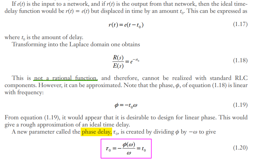
Clifford E. Cummings, Simulation and Synthesis Techniques for
Asynchronous FIFO Design with Asynchronous Pointer Comparisons [pdf]
TODO 📅
Scrambler
TODO 📅
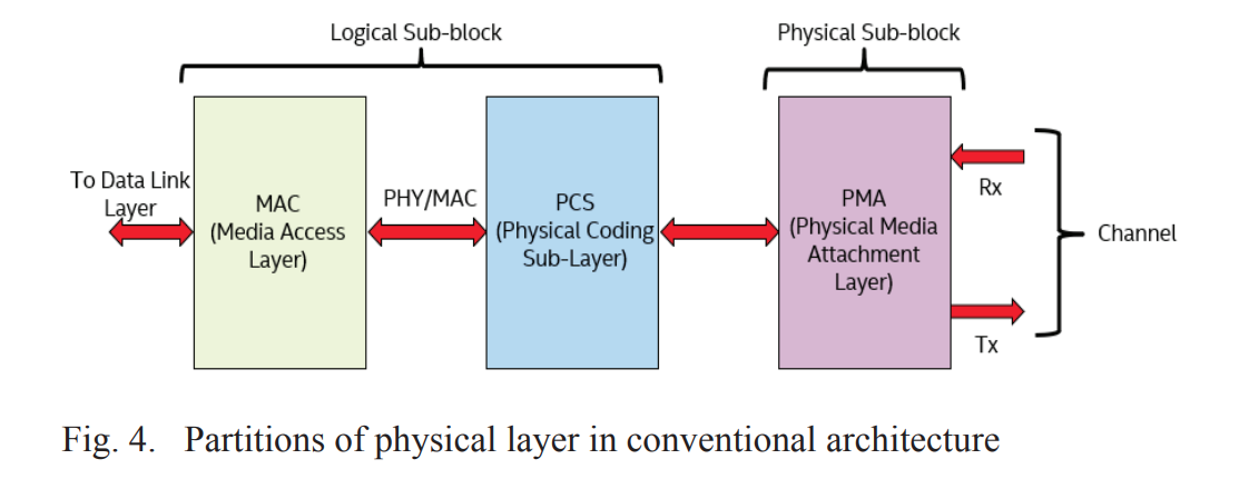
Link Training and
Initialization (LTSSM)
TODO 📅
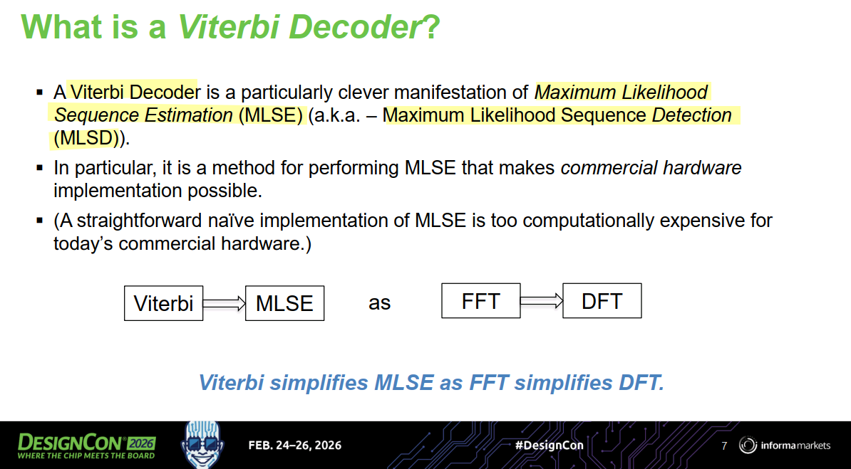
Viterbi-based MLSD
M. Emami Meybodi, H. Gomez, Y. -C. Lu, H. Shakiba and A.
Sheikholeslami, "Design and Implementation of an On-Demand
Maximum-Likelihood Sequence Estimation (MLSE)," in IEEE Open Journal of
Circuits and Systems, vol. 3, pp. 97-108, 2022 [https://sci-hub.jp/10.1109/OJCAS.2022.3173686]
Zaman, Arshad Kamruz (2019). A Maximum Likelihood Sequence Equalizing
Architecture Using Viterbi Algorithm for ADC-Based Serial Link.
Undergraduate Research Scholars Program. Available electronically from
[https://hdl.handle.net/1969.1/166485]
S. Song, K. D. Choo, T. Chen, S. Jang, M. P. Flynn and Z. Zhang, "A
Maximum-Likelihood Sequence Detection Powered ADC-Based Serial Link," in
IEEE Transactions on Circuits and Systems I: Regular Papers,
vol. 65, no. 7, pp. 2269-2278, July 2018 [https://sci-hub.jp/10.1109/TCSI.2017.2775619]
Vineel Kumar Veludandi. Maximum likelihood sequence estimation (MLSE)
using the Viterbi algorithm [https://github.com/vineel49/mlse]
David Banas, Keysight, DesignCon 2026, Tutorial – Understanding
the Viterbi Decoder
—, ISSCC2007 T10: Fundamentals of Electronic Dispersion Compensation
(EDC)
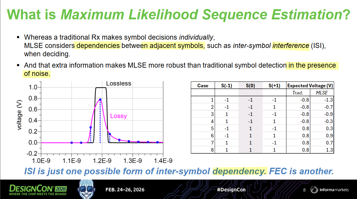
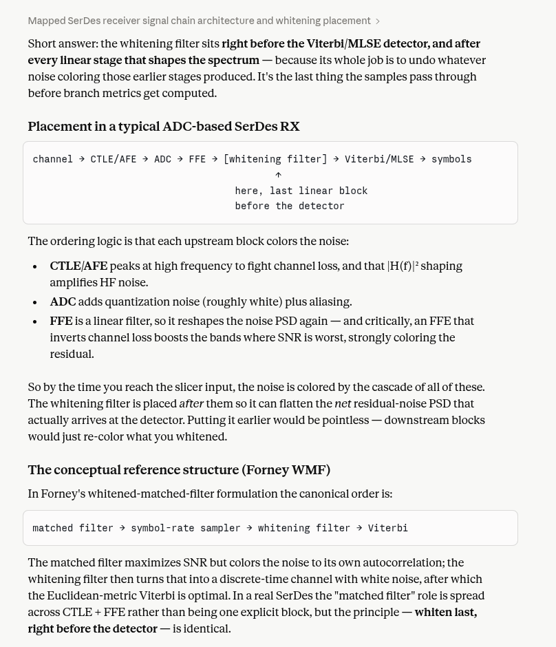
Maximum-Likelihood Sequence Detection performed by
Viterbi on the ISI trellis induced by
the channel
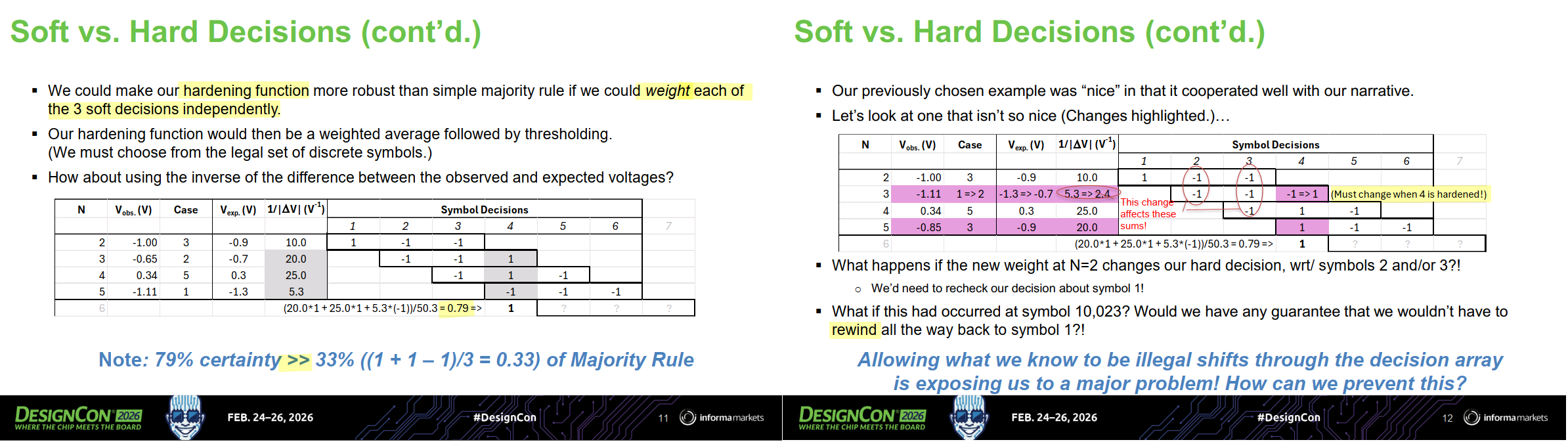
Simple soft-decision voting
Simple soft-decision voting can use more information than a slicer,
but without a trellis/path-consistency rule, it can create impossible or
unstable decision histories.
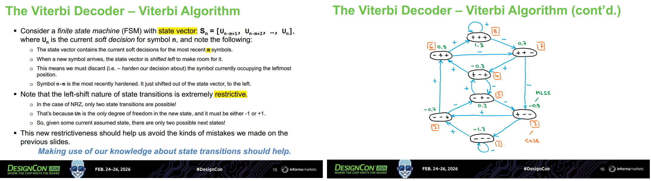
Viterbi Decoder
Pre-cursor \(h_{-1}=0.3\), Current
(main) cursor \(h_0=0.8\), Post-cursor
\(h_1=0.2\)
trellis depth = N = 3 (consistent with 8 states);
the 4 is the number of observation samples in that
particular walk-through, i.e. the time axis — a different thing that
unfortunately shares the label "N" on the slide
As currently built, ViterbiDecoder_ISI models
post-cursor ISI only. _states[ix][-1]
selecting the last element as the current symbol is consistent with
that
DFE (kept light): recover timing, slice
levels→bits, and optionally trim the far ISI tail beyond the
trellis window — but not aggressively cancel the near
post-cursors.
Viterbi: handle the near post-cursor ISI (the
cursor + N−1 taps) that was intentionally left in, via MLSE —
which tolerates a closed eye where the DFE's hard decisions would
error-propagate
Group
Members
When set
Role
Static model
_states, _expecteds, _trans,
_sigma, _v_prob
once, in __init__
the time-invariant channel/decoder description
Dynamic state
_trellis
mutated every step_trellis
the evolving survivor metrics/back-pointers
All three derive purely from the constructor args
(L, N, pulse_resp_samps):
_states — the Lᴺ
symbol-window combinations (all_combs). Fixed because the
alphabet and memory depth don't change.
_expecteds — the noiseless expected
sample per state, Σ h[n]·s[-(n+1)]. Fixed because it bakes
in pulse_resp_samps (the ISI taps).
_trans — the shift-register adjacency
(which state can follow which), as a row-normalized PMF. Fixed because
the trellis topology is structural, independent of data.
classViterbiDecoder_ISI(ViterbiDecoder[State_ISI, float]): """ Viterbi decoder using ISI to define observation probabilities. """
# pylint: disable=too-many-locals def__init__(self, L: int, N: int, sigma: float, pulse_resp_samps: Rvec): """ Args: L: Number of symbol voltage levels. N: Number of symbols per state. sigma: Standard deviation of Gaussian voltage noise (V). pulse_resp_samps: Upstream channel pulse response samples, one per UI, beginning with cursor (V). (Must have length >= ``N``!) """
vs = np.linspace(-2, 2, 4_000) # voltage-error grid: −2..+2 V, 4000 pts → ~1 mV spacing v_prob = sp.interpolate.interp1d( vs, [1e-3 * np.exp(-(v**2)/(2*sigma**2)) / np.sqrt(TWOPI*sigma**2) for v in vs], bounds_error=False, fill_value=0)
# bounds_error=False, fill_value=0 → any error magnitude beyond ±2 V returns probability 0 (treated as impossible — way outside the noise distribution)
defprob(self, s: int, x: float) -> float: """ Probability of state at index ``s`` given observation ``x``. """ returnself.v_prob(x - self.expectation(s))
v_prob(δ) returns the probability (density) of seeing a
noise voltage error δ under a zero-mean Gaussian with
standard deviation sigma. It's the emission
probability of the Viterbi algorithm.
In short: v_prob is the decoder's noise model — a fast
Gaussian-likelihood lookup that converts "how far is this sample from
what state s predicts?" into "how probable is that?", which
is exactly the data-driven term the Viterbi trellis needs
classViterbiDecoder(ABC, Generic[S, X]): """ Abstract definition of a Viterbi decoder. """ defstep_trellis(self, x: X, priming: bool = False) -> int: """ Shift the trellis one column left, using the given observation sample. Args: x: The new observation sample. Keyword Args: priming: Don't perform backtrace when True. Default: False Returns: The decided state index of the exiting (i.e. - leftmost) column. """
The core Viterbi recursiontrellis[-1][r][0] * self.trans[r][s] * self.prob(s, x) —
the candidate path metric for arriving at current state s
through predecessor r\[
P(r \to s \mid x) = \underbrace{\text{trellis}[-1][r][0]}{\text{(1)
survivor prob of } r} \times \underbrace{\text{trans}[r][s]}{\text{(2)
transition } r\to s} \times \underbrace{\text{prob}(s, x)}_{\text{(3)
emission of } s}
\]
trellis[-1][r][0] — the survivor probability of
the predecessor state r
self.trans[r][s] — the transition probability
r → s
self.prob(s, x) — the emission probability of
current state s given observation
x
path performs the back-trace
(trace-back) step of the Viterbi algorithm: starting from the
most-likely state in the newest column, it follows the back-pointers
leftward through the trellis to recover the maximum-likelihood
sequence of states held in the current window.
classViterbiDecoder(ABC, Generic[S, X]): """ Abstract definition of a Viterbi decoder. """
@property defpath(self) -> list[int]: """ Maximum likelihood forward path through the trellis. Notes: 1. First element in returned list corresponds to the time just before the first trellis column. 2. The decided state of the final trellis column is *not* included. """
# Starting with highest probability final state, backtrack through trellis. prevs = [trellis[-1][np.argmax(list(map(lambda pr: pr[0], trellis[-1])))][1]] for ix inrange(2, trellis_depth + 1): prevs.append(trellis[-ix][prevs[-1]][1]) prevs.reverse() return prevs
At the end you drain the N−1 symbols still sitting in
the trellis
""" Standalone demo: run the PyBERT Viterbi (ISI) decoder on a synthetic link. Builds a ``ViterbiDecoder_ISI`` for a 2-level (NRZ) channel with strong post-cursor ISI, generates a noisy received waveform, decodes it via maximum likelihood sequence estimation (MLSE), and compares the error count against a naive symbol-by-symbol slicer. Run (from the repository root):: PYTHONPATH=src python examples/run_viterbi.py This example depends only on ``numpy``/``scipy`` -- not on the optional ``pyibisami`` dependency. """
import numpy as np
from pybert.models.viterbi import ViterbiDecoder_ISI
rng = np.random.default_rng(42)
# --- Link / decoder parameters --- L = 2# NRZ (2 levels: -1, +1) N = 2# symbols of memory per state sigma = 0.22# Gaussian noise std-dev (V) pulse_resp = np.array([1.0, 0.8]) # cursor + strong post-cursor ISI tap (V/UI)
dec = ViterbiDecoder_ISI(L=L, N=N, sigma=sigma, pulse_resp_samps=pulse_resp) expecteds = [dec.expectation(i) for i inrange(len(dec.states))] print(f"States ({len(dec.states)}): {dec.states}") print(f"Expected observations: {np.round(expecteds, 3)}") print(f"State Transition Probability matrix:\n{dec.trans}\n")
# --- Generate a random NRZ symbol stream (-1/+1) --- n_syms = 5000 levels = np.array([-1.0, 1.0]) tx = rng.choice(levels, size=n_syms)
# --- Pass through the ISI channel + add noise to make the received waveform --- clean = np.convolve(tx, pulse_resp)[:n_syms] rx = clean + rng.normal(0.0, sigma, size=n_syms)
# --- Decode --- state_idxs = dec.decode(list(rx)) # Each decoded state is an N-symbol vector; the current symbol is its last element. decoded = np.array([dec.states[i][-1] for i in state_idxs])
# Align (decoder output corresponds to the symbol stream) and count errors. m = min(len(tx), len(decoded)) errs = int(np.sum(tx[:m] != decoded[:m]))
# --- Compare against a naive symbol-by-symbol slicer (threshold at 0) --- slicer = np.where(rx > 0, 1.0, -1.0) slicer_errs = int(np.sum(tx[:m] != slicer[:m]))
Partial Response Signaling (PRS) and Maximum Likelihood Sequence
Detection (MLSD) are paired together to maximize data rates in
bandwidth-limited, noisy channels like fiber optics, magnetic hard
drives, and high-speed backplanes
Flit (flow control unit)
TODO 📅
FBER (First Bit Error Rate)
TODO 📅
1 2
FBER is like BER except that, for example, a 10-bit burst error counts as one FBER but would count as 10 BER. The FEC in Flit Mode can correct up to a single 16-bit burst error in any given Flit.
Note that the PCIe FEC is weak as compared to Ethernet. This is intentional. Stronger FEC codes incur higher latency penalty (because they cover more bits and require more computation). PCIe Links are short and replays are quick. The tradeoff was made that additional delay due to an occasional replay was preferable to a constant delay due to a more powerful FEC. The PCIe FEC's purpose is to reduce the replay rate to an acceptable level, not eliminate replays. Ethernet has longer Links with longer replay times. That motivates their different tradeoff.
TODO 📅
Feature
Intersymbol Interference (ISI)
Forward Error Correction (FEC)
Definition
A signal distortion where symbols
overlap.
A coding technique to detect/fix bit
errors.
Origin
Unintentional (caused by
channel physics).
Intentional (added by the
system designer).
Data Impact
Smears pulses together, making them
unreadable.
Adds redundant bits to protect original
data.
Primary Cause
Multipath fading and limited
bandwidth.
Noise, interference, and signal
attenuation.
Relationship
Negative dependency (interference).
Positive dependency (structured
redundancy).
Typical Solution
Equalization or Pulse Shaping (e.g.,
Root-Raised Cosine).
Block Codes (Reed-Solomon) or
Convolutional Codes (LDPC).
Goal
To clean the signal
before decoding.
To recover the data after
decoding errors.
Reed-Solomon (RS) codes
RS is a forward error-correction (FEC) algorithm
used to correct data corruption after it has been received
ECC (Error Control Coding)
Takayuki Kawahara, ISSCC2007 T5: Error-Correcting Codes for
Memories
TODO 📅
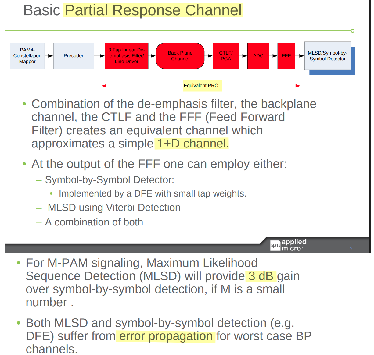
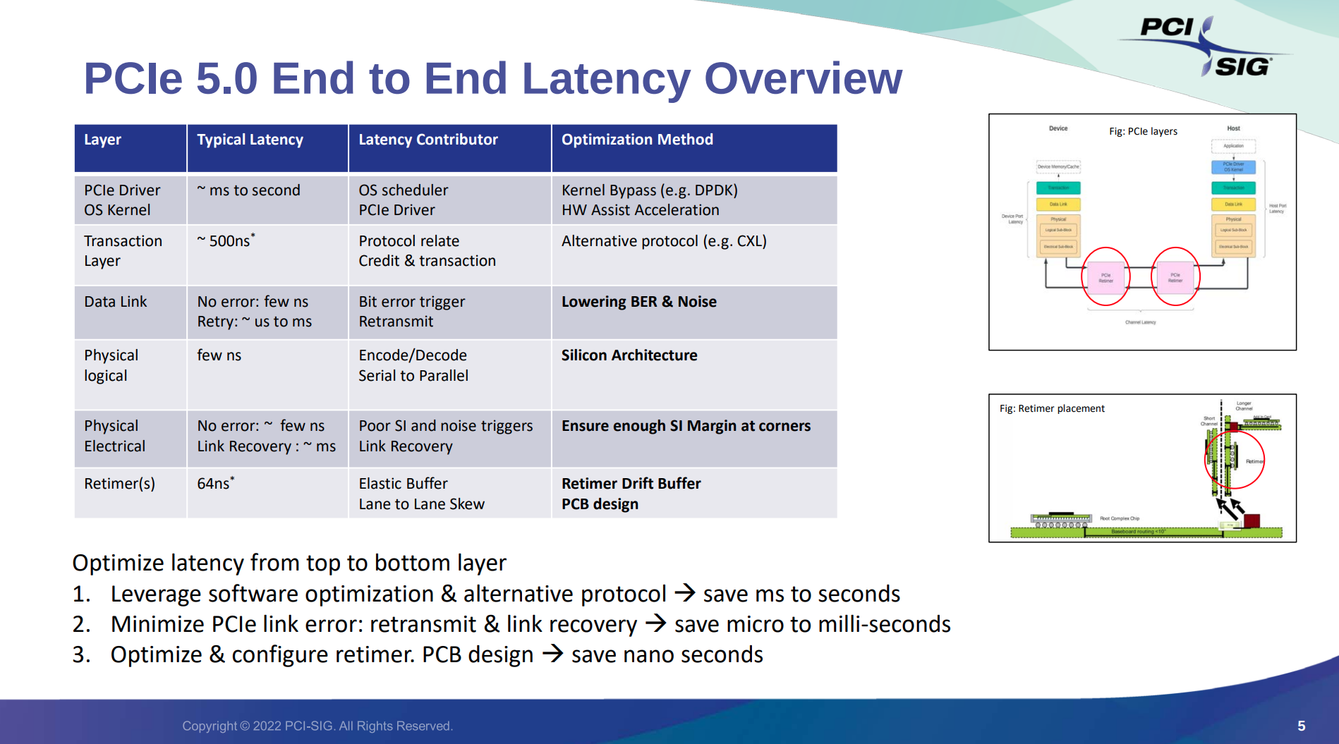
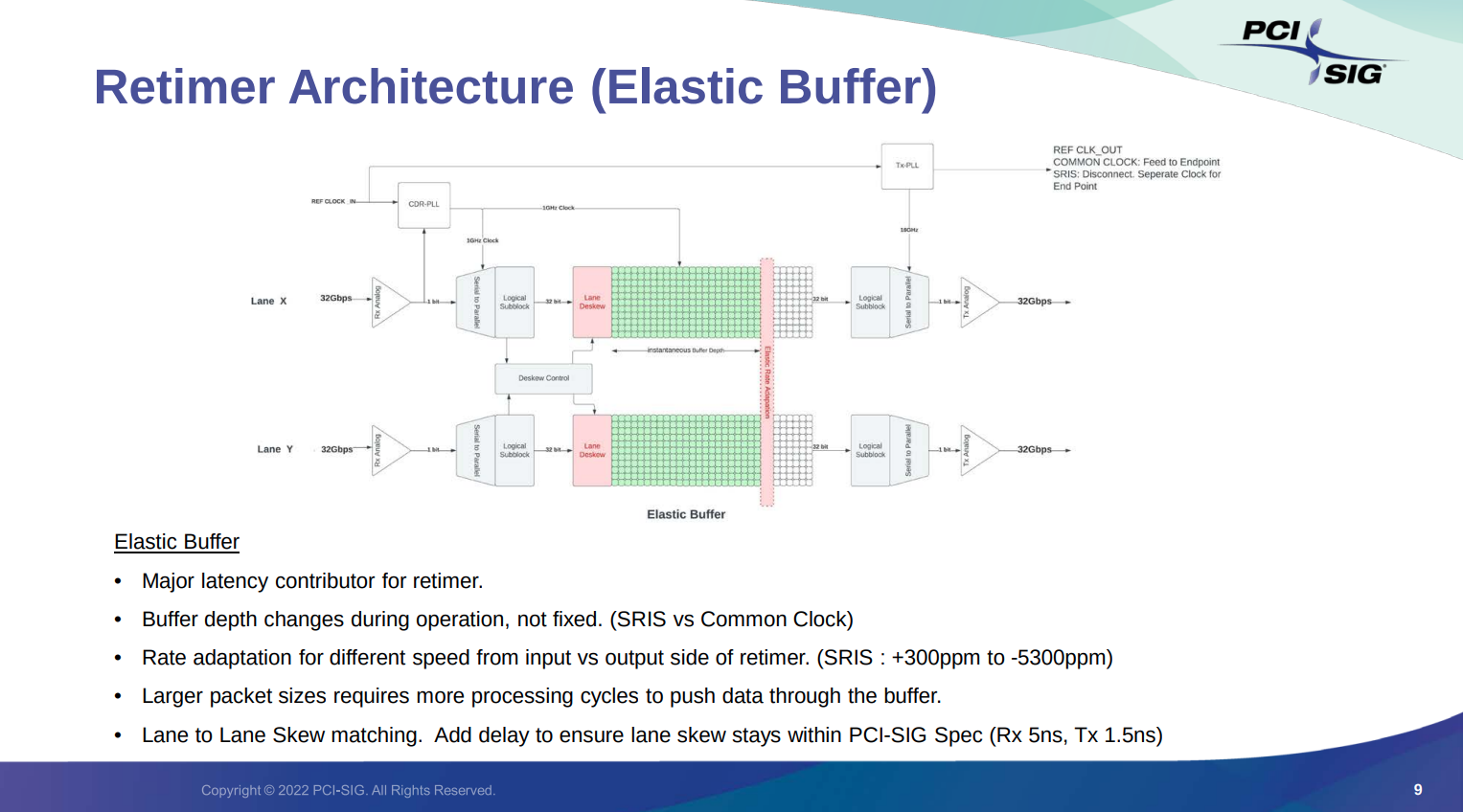
PCIe® Retimer Latency
Jay Li, Product Marketing Director, kandou, T3S02_PCIe Retimer
Latency
PCI Express Standards
Information
CLB: Compliance Load Board (System Board)
CBB: Compliance Base Board (Add-in Card)
NCB (Non-ChangeBar): A clean version of the official
specification document that contains the full text of the updated
standard
CB (ChangeBar): A version that highlights only the
changes and additions made from the previous version of the
specification. The added or modified lines typically have a vertical bar
(a changebar) in the margin for easy scanning
Base Specification: The PCI Express Base describes
the architecture, interconnect attributes, fabric management, and the
programming interface required to design and build systems and
peripherals that are compliant with the PCI Express Specification.
CEM (Card Electromechanical) Specification: The PCI
Express CEM specifications define an implementation for small form
factor PCI Express cards
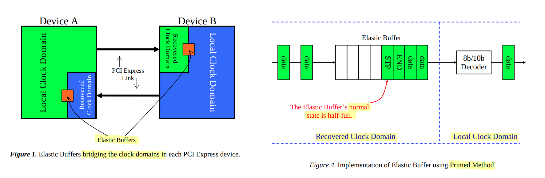
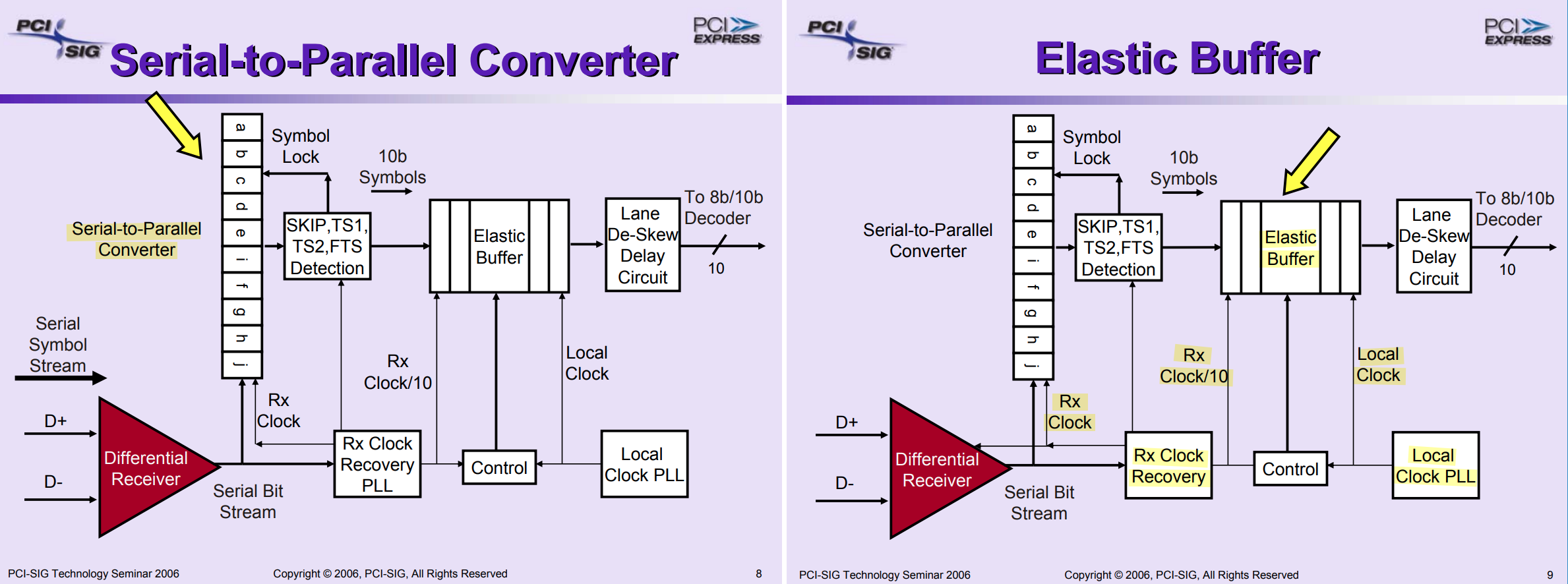
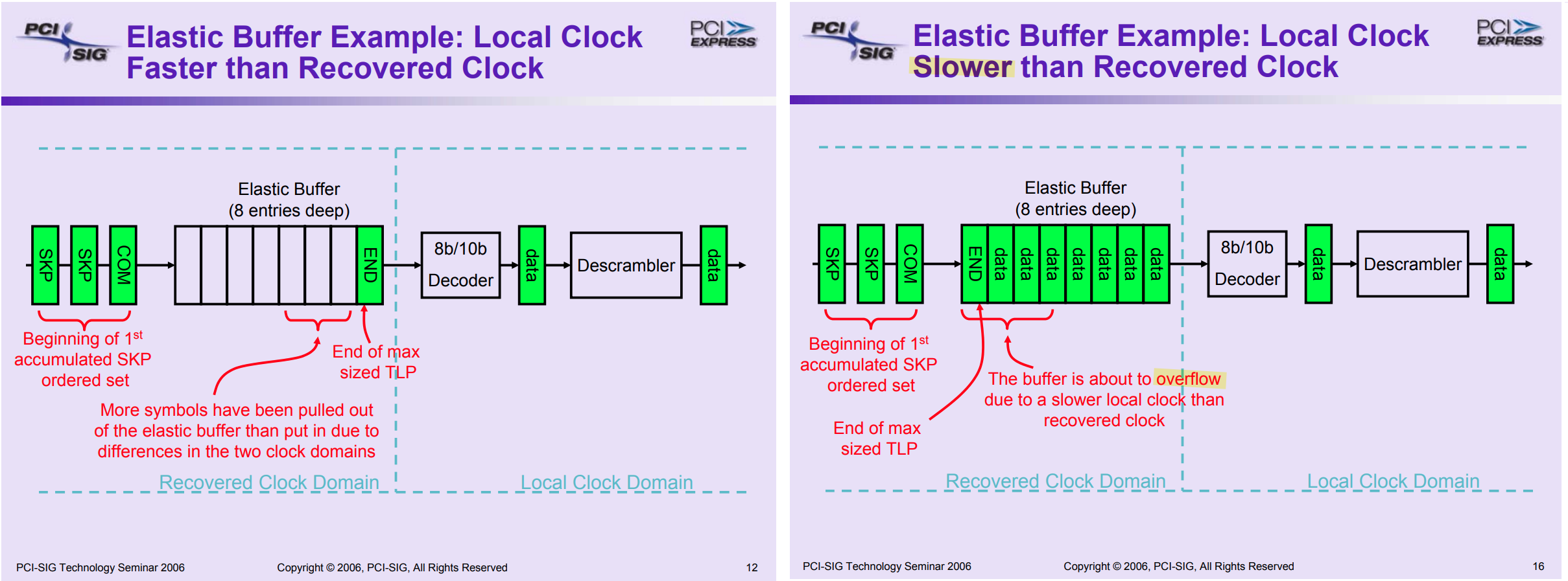
Kamesh Velmail, Samsung, Challenges, Complexities and Advanced
Verification Techniques in Stress Testing of Elastic Buffer in High
Speed SERDES IPs [pdf]
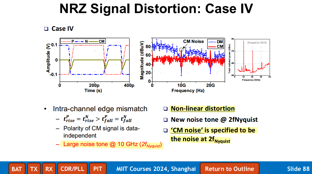
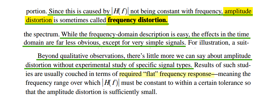
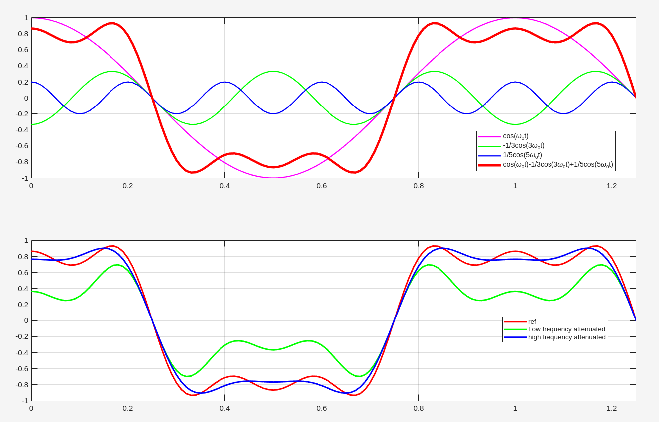
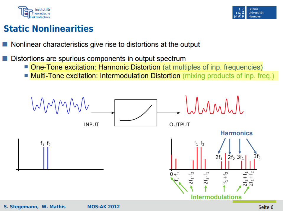
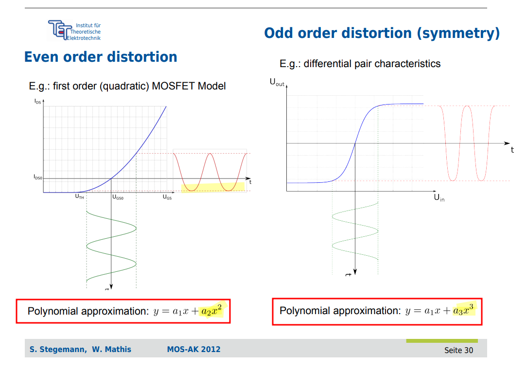
Linear distortion includes any
amplitude or delay distortion associated with a linear
transmission system
Nonlinear distortion includes harmonic
distortion, intermodulation distortion (IMD)
CM Noise
Luo, X., Yu, H., Maqbool, K. Q., Huang, Y., Luo, D., & Yue, P. C.
(2017). Analysis on EMI Related Common-mode Noise of Serdes Transmitter.
Paper presented at DesignCon 2017 [lnk]
—. EMI related common-mode noise analysis in high-speed backplane
links. Thesis (Ph.D.)-HKUST 2018 [link]
—. Study on the effects of distortions and common‐mode noise in
high‐speed PAM‐4 systems - Luo - 2018 - Electronics Letters - Wiley
Online Library [link]
Patrick Yue. MIIT Courses 2024, Shanghai. Advanced Wireline and
Optical Communication IC Design [pdf]
Lee, Jri & Chiang, Ping-Chuan & Peng, Pen-Jui & Chen,
Li-Yang & Weng, Chih-Chi. (2015). Design of 56 Gb/s NRZ and PAM4
SerDes transceivers in CMOS technologies. IEEE Journal of Solid-State
Circuits. [pdf]
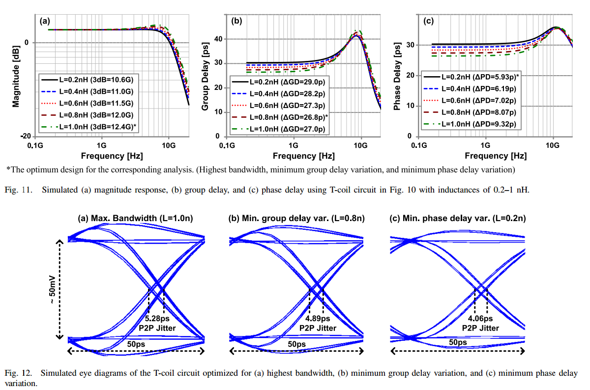
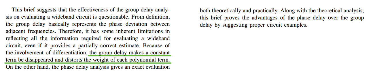
W. Bae, B. Nikolić and D. -K. Jeong, "Use of Phase Delay Analysis for
Evaluating Wideband Circuits: An Alternative to Group Delay Analysis,"
in IEEE Transactions on Very Large Scale Integration (VLSI) Systems,
vol. 25, no. 12, pp. 3543-3547, Dec. 2017, [https://people.eecs.berkeley.edu/~bora/Journals/2017/TVLSI17.pdf]
Hollister, Allen L. Wideband Amplifier Design. Raleigh, NC:
SciTech Pub., 2007.
Starič, P. & Margan, E.. (2006). Wideband Amplifiers.
10.1007/978-0-387-28341-8. [pdf]
Haykin, Simon S., and Michael Moher. Communication Systems.
5th ed. John Wiley & Sons, 2009.
—. Digital Communication Systems. 1st edition. Wiley, 2013.
[pdf]
Carlson, A. Bruce, and Paul B. Crilly. Communication Systems: An
Introduction to Signals and Noise in Electrical Communication. 5th
ed. Boston: McGraw-Hill Higher Education, 2010. [pdf]
B. Razavi, "Design considerations for direct-conversion receivers,"
in IEEE Transactions on Circuits and Systems II: Analog and Digital
Signal Processing, vol. 44, no. 6, pp. 428-435, June 1997 [http://www.seas.ucla.edu/brweb/papers/Journals/RTCAS97.pdf]
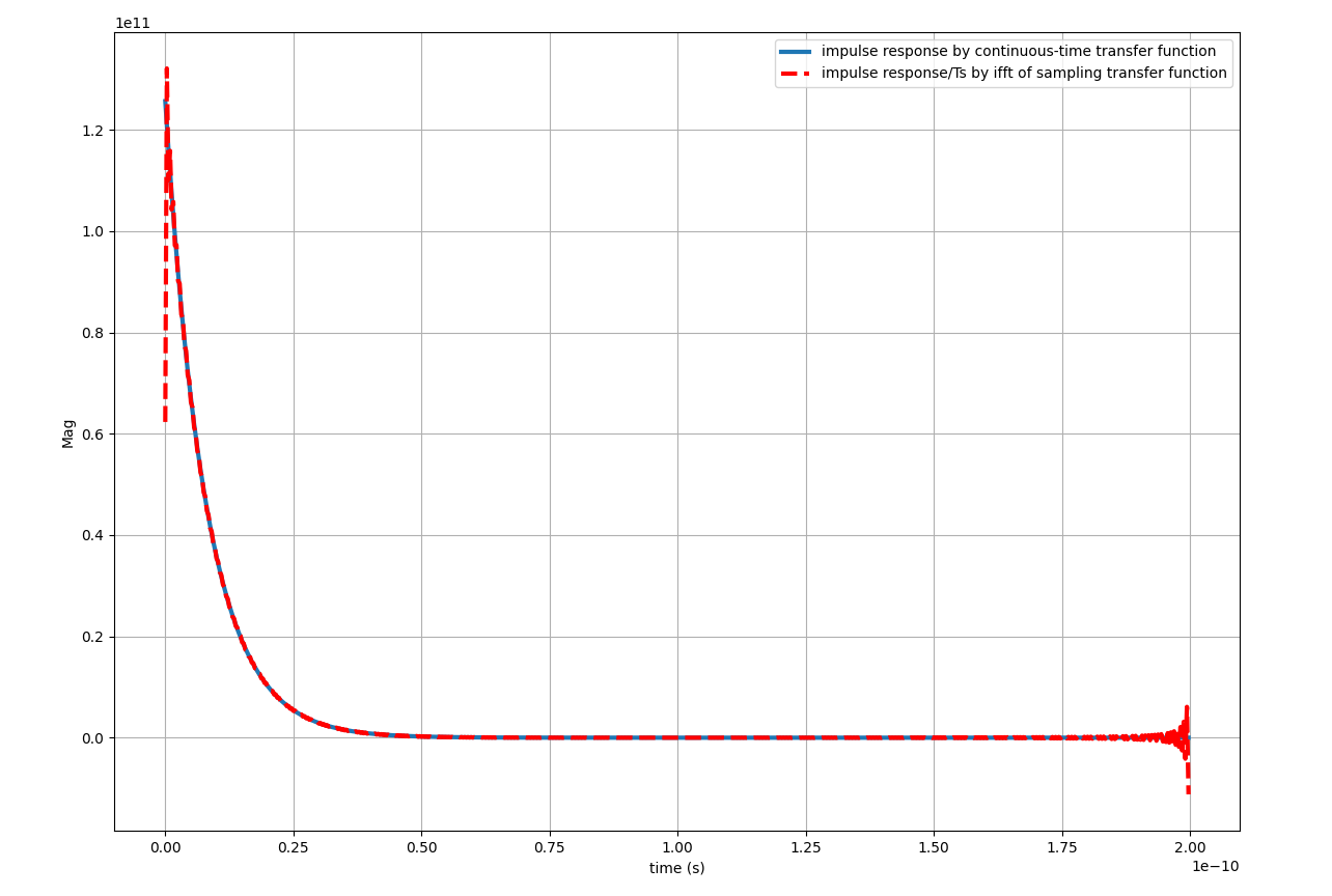
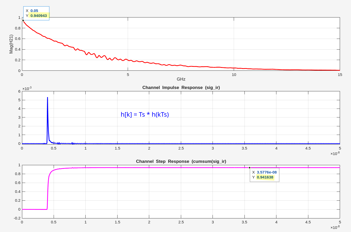
ifft of sampling continuous-time transfer
function
1 2 3 4 5 6 7 8 9 10 11 12 13 14
deffreq2impulse(H, f): #Returns the impulse response, h, and (optionally) the step response, #hstep, for a system with complex frequency response stored in the array H #and corresponding frequency vector f. The time array is #returned in t. The frequency array must be linearly spaced.
Hd = np.concatenate((H,np.conj(np.flip(H[1:H.size-1])))) h = np.real(np.fft.ifft(Hd)) #hstep = sp.convolve(h,np.ones(h.size)) #hstep = hstep[0:h.size] t= np.linspace(0,1/f[1],h.size+1) t = t[0:-1]
return h,t
Maybe, the more straightforward method is sampling impulse response
of continuous-time transfer function directly
## freq2impulse(H, f), ifft - using sample of continuous-time tranfer function f = w/(2*np.pi) Hd = np.concatenate((H,np.conj(np.flip(H[1:H.size-1])))) hd = np.real(np.fft.ifft(Hd)) t= np.linspace(0,1/f[1],hd.size+1) t = t[0:-1]
## continuous-time transfer function - impulse t, hc = signal.impulse(([1], [1/wbw, 1]), T = t)
## hd(kTs) = Ts*hc(kTs) plt.figure(figsize = (14,10)) plt.plot(t, hc, t, hd/Ts, '--r', linewidth=3) plt.grid(); plt.legend(['impulse response by continuous-time transfer function','impulse response/Ts by ifft of sampling transfer function']) plt.ylabel('Mag'); plt.xlabel('time (s)'); plt.show()
#oversampled signal signal_ideal = np.repeat(signal_BR, samples_per_symbol)
#eye diagram of ideal signal sdp.simple_eye(signal_ideal, samples_per_symbol*3, 100, dt, "{}Gbps 2-PAM Signal".format(data_rate/1e9),linewidth=1.5, res=200)
#max frequency for constructing discrete transfer function max_f = 1/dt
#max_f in rad/s max_w = max_f*2*np.pi
#heuristic to get a reasonable impulse response length ir_length = int(4/(freq_bw*dt))
#calculate discrete transfer function of low-pass filter with pole at freq_bw w, H = sp.signal.freqs([freq_bw*(2*np.pi)], [1,freq_bw*(2*np.pi)], np.linspace(0,0.5*max_w,ir_length*4))
#find impluse response of low-pass filter h, t = sdp.freq2impulse(H,f)
defshift_signal(signal, samples_per_symbol): """Shifts signal vector so that 0th element is at centre of eye, heuristic Parameters ---------- signal: array signal vector at RX samples_per_symbol: int number of samples per UI Returns ------- array signal shifted so that 0th element is at centre of eye """ #Loss function evaluated at each step from 0 to steps_per_signal loss_vec = np.zeros(samples_per_symbol) for i inrange(samples_per_symbol): samples = signal[i::samples_per_symbol] #add loss for samples that are close to threshold voltage loss_vec[i] += np.sum(abs(samples)**2) #find shift index with least loss shift = np.where(loss_vec == np.max(loss_vec))[0][0] # plt.plot(np.linspace(0,samples_per_symbol-1,samples_per_symbol),loss_vec) # plt.show() return np.copy(signal[shift+1:])
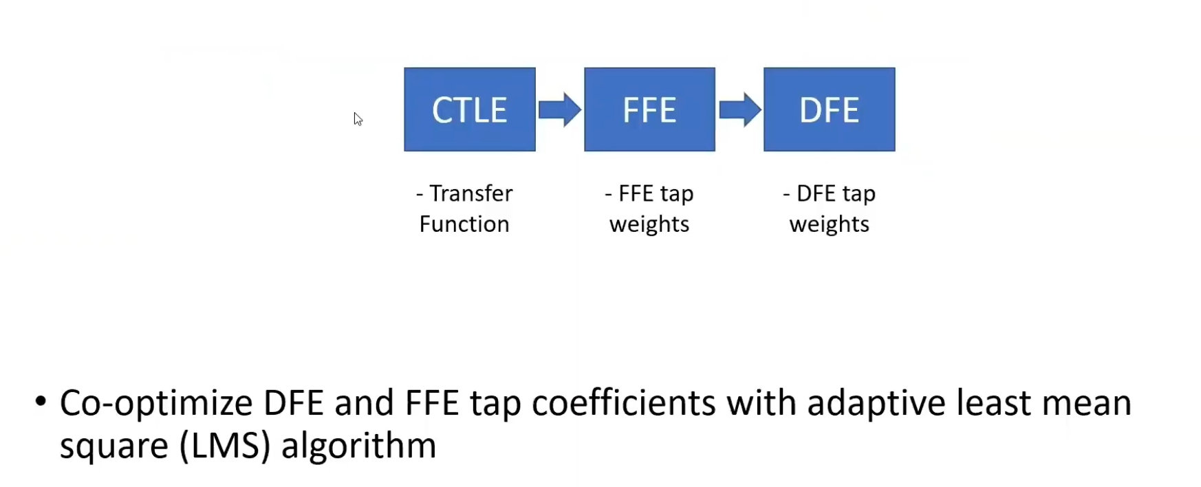
lms_equalizer performs offline
adaptation and it fail due to DFE Error Propagation if
reference is None\[
\underbrace{\mathbf{y}_k}_{\text{FFE input}}
\;\xrightarrow{\;\langle\cdot,\mathbf{w}_{\text{ffe}}\rangle\;}\;
v^{\text{ffe}}_k
\;\xrightarrow{\;-\,\langle\mathbf{z}_k,\mathbf{w}_{\text{dfe}}\rangle\;}\;
v^{\text{dfe}}_k
\;\xrightarrow{\;Q(\cdot)\;}\;
z_k
\]
deflms_equalizer(y, mu, N, w_ffe, FFE_pre, w_dfe, voltage_levels, alpha=None, reference=None, update_rate=1): """ voltage_levels: array discrete voltage levels to use in DFE optimization alpha: array (optional) used to fix the first `len(alpha)` weights in `w_dfe`, starting from the first pre-tap. these weights will not be optimized and will stay constant throughout LMS updates. reference: array (optional) if provided, LMS will attempt to optimize according to the error between the signal and reference, rather than estimating it based on the cloest voltage level. `len(reference)` may be less than `len(y)`, in which case only the first `len(reference)` updates will be optimized in this manner. """ e = np.zeros(N) v_ffe = np.zeros(N) # signal computed after FFE optimization v_dfe = np.zeros(N) # signal computed after FFE and DFE optimization z = np.zeros(N) # signal quantized from v_dfe min_delay = max(FFE_post, DFE_taps) for k inrange(min_delay, N - FFE_pre): y_k = y[k - FFE_post:k + FFE_pre + 1][::-1] z_k = z[k - DFE_taps:k][::-1]
# alpha takes over the first len(alpha) terms of w_dfe if is_cooptimizing and alpha isnotNone: w_dfe[:len(alpha)] = alpha
defFFE(self,tap_weights, n_taps_pre): """Behavioural model of FFE. Input signal is self.signal, this method modifies self.signal Parameters ---------- tap_weights: array DFE tap weights n_taps_pre: int number of precursor taps """
defprqs10(seed): """Genterates PRQS10 sequence Parameters ---------- seed : int seed used to generate sequence should be greater than 0 and less than 2^20 Returns ------- array: PRQS10 sequence """ a = prbs20(seed) shift = int((2**20-1)/3) b = np.hstack((a[shift:],a[:shift])) c = np.vstack((a,b)) # c[0,:] MSB, c[1,:] LSB
pqrs = np.zeros(a.size,dtype = np.uint8) for i inrange(a.size): pqrs[i] = grey_encode(c[:,i]) return pqrs
defprqs12(seed): a = prbs24(seed) shift = int((2**24-1)/3) b = np.hstack((a[shift:],a[:shift])) c = np.vstack((a,b))
pqrs = np.zeros(a.size,dtype = np.uint8) for i inrange(a.size): if (i%1e5 == 0): print("i =", i) pqrs[i] = grey_encode(c[:,i]) return pqrs
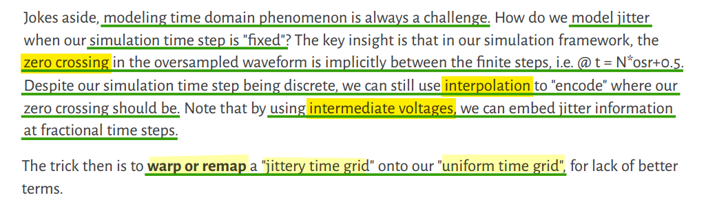
Gaussian distribution jitter
TX signal with jitter
The accuracy of the jitter model is constrained by the
resolution defined as
sample_time = UI/samples_per_symbol within the
gaussian_jitter implementation.
defgaussian_jitter(signal_ideal, UI,n_symbols,samples_per_symbol,stdev): """Generates the TX waveform from ideal, square, self.signal_ideal with jitter Parameters ---------- signal_ideal: array ideal,square transmitter voltage waveform UI: float length of one unit interval in seconds n_symbols: int number of symbols in signal_ideal samples_per_symbol: int number of samples in signal_ideal corresponding to one UI stdev: standard deviation of gaussian jitter in seconds stdev_div_UI : float standard deviation of jitter distribution as a pct of UI """
function gen_wvfm(bits; tui, osr) #helper function used to generate oversampled waveform Vbits = kron(bits, ones(osr)) #Kronecker product to create oversampled waveform dt = tui/osr tt = 0:dt:(length(Vbits)-1)*dt
return tt, Vbits end
first order RC response, normalized to the time
step\[
\frac{\alpha}{s+\alpha} \overset{\mathcal{L}^{-1}}{\longrightarrow}
\alpha\cdot e^{-\alpha t}
\]
The integral of impulse response of low pass RC filter \(\int_{0}^{+\infty} \alpha\cdot e^{-\alpha t}dt =
1\) — sum(ir*dt)
1 2 3 4 5 6 7 8 9 10 11
function gen_ir_rc(dt,bw,t_len) #helper function that directly calculates a first order RC response, normalized to the time step tt = [0:dt:t_len-dt;]
#checkout the intuitive symbols! ω = (2*π*bw) ir = ω*exp.(-tt*ω) ir .= ir/sum(ir*dt)
return ir end
sum(ir)*dt = 1, i.e. the step response
1
1 2
out = conv(ir, vbits)*tui/osr lines(tt, out[1:length(vbits)])
1 2 3 4 5 6 7 8 9 10 11 12
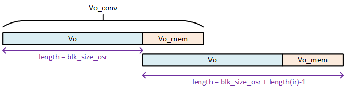
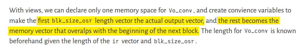
#call our convolution function; let's keep the input memory zero for now #change the drv parameters in the struct definition to see the waveform/eye change u_conv!(drv.Vo_conv, Vosr, drv.ir, Vi_mem=zeros(1), gain = drv.swing * param.dt);
#we will also create a non-mutating u_conv function for other uses function u_conv(input, ir; Vi_mem = zeros(1), gain = 1) vconv = gain .* conv(ir, input) vconv[eachindex(Vi_mem)] += Vi_mem
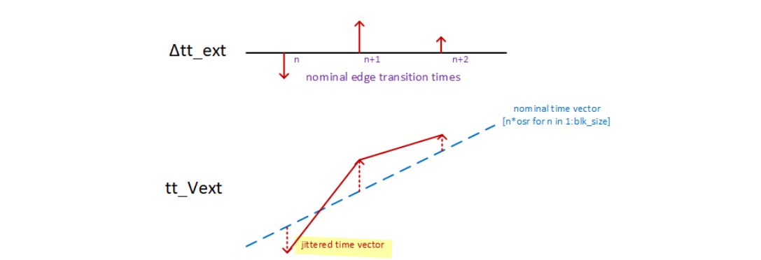
Because each symbol's width is determined by two
edges, \(\Delta tt\_\text{ext}\) is is
one greater than \(V_\text{ext}\)
1 2 3 4 5 6 7 8 9 10
function drv_jitter_tvec!(tt_Vext, Δtt_ext, osr) for n = 1:lastindex(Δtt_ext)-1 tt_Vext[(n-1)*osr+1:n*osr] .= LinRange((n-1)*osr+Δtt_ext[n], n*osr+Δtt_ext[n+1], osr+1)[1:end-1] end
itp = linear_interpolation(drv.tt_Vext, drv.Vext); #itp is a function object
itp = linear_interpolation(drv.tt_Vext, drv.Vext) create
linear interpolation only, extrapolation shall
not be used to avoid inducing any error
1 2 3 4 5
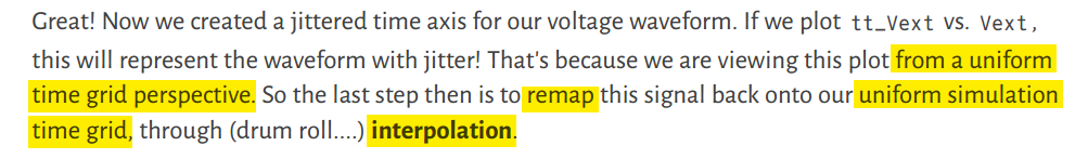
#note here tt_uniform is shifted by prev_nui/2 to give wiggle room for sampling "before" and "after" the current block. This is necessary for sinusoidal jitter tt_uniform = (0:param.blk_size_osr-1) .+ drv.prev_nui/2*param.osr;
#To interpolate, use the itp object like a function and broadcast to a vector Vfir = itp.(tt_uniform);
tt_uniform is shifted by prev_nui/2 to give
wiggle room for sampling "before" and "after" the current block.
This is necessary for sinusoidal jitter
DCD and RJ have much smaller shifts (typically <1 UI), but SJ can
oscillate over multiple UI widths, requiring this centered
offset to prevent interpolation boundary errors.
1 2 3 4 5 6 7 8 9 10 11 12
function drv_jitter_tvec!(tt_Vext, Δtt_ext, osr) for n = 1:lastindex(Δtt_ext)-1 # Starting from 0 tt_Vext[(n-1)*osr+1:n*osr] .= LinRange((n-1)*osr+Δtt_ext[n], n*osr+Δtt_ext[n+1], osr+1)[1:end-1] # drop the last end
returnnothing end
# Starting from 0 tt_uniform::Vector = (0:param.blk_size_osr-1) .+ prev_nui/2*param.osr
This creates tt_Vext starting from
(n-1)*osr, which means:
First segment: 0*osr + offset to
1*osr + offset = starts at 0
Second segment: 1*osr + offset to
2*osr + offset
etc.
tt_uniform must align with this same time
scale for interpolation to work correctly.
Starting from 0 ensures tt_uniform
aligns with the OSR sample grid and matches the time values in
tt_Vext for correct interpolation.
\[
\sigma_n^2 = 4\cdot k_B T \cdot R \cdot \frac{f_s}{2} = k_B T \cdot R
\cdot 2f_s= \frac{\color{red}{2}}{T_s} \cdot 10^{\frac{-174 - 30}{10}}
\cdot R
\]
noise_rms::Float64 = sqrt(2/param.dt*10^((noise_dbm_hz-30.0)/10)
rather than
sqrt(0.5/param.dt*10^((noise_dbm_hz-30.0)/10)
The margin of 10 (pi_max_code - 10)
ensures that even if the CDR makes a moderately large step (up to ±10
codes), it won't be mistaken for a wrap. This is safe as long as the CDR
loop bandwidth is low enough that per-update code changes stay well
below 10
1 2 3 4 5 6 7 8 9 10 11 12 13 14 15 16
function clkgen_pi_itp_top!(clkgen; pi_code)
Δpi_code = pi_code-pi_code_prev if abs(Δpi_code) > pi_wrap_ui_Δcode pi_wrap_ui -= sign(Δpi_code)*pi_ui_cover end
pi_wrap_ui accumulates full UI wraps across blocks.
Combined with Φstart = (cur_subblk-1)*subblk_size*osr (the
sub-block offset), this means Φo_subblk coordinates are in
the global sample coordinate system relative to the
start of the current block — which is exactly what
tt_Vext's centered coordinate system expects
1
2
3
4
5
6
7
8
9
10
11
12
13
14
function cdr_top!(cdr, Sd, Se)
for n = findall(eslc_nvec.!=0) if Sd_val[n:n+2] in filt_patterns vote = sign(Se[n][1].-0.5)*sign(Sd_val[n]-Sd_val[n+2]) ki_accum += ki*vote pd_accum += pd_gain*(kp*vote + ki_accum) end end
Wraps pd_accum into [0, pi_bnd) (i.e.,
[0, 256) for 8-bit PI), then floors it to produce the
integer pi_code that feeds back to
clkgen_pi_itp_top!. This is the modular
accumulator — the same wrapping that
pi_wrap_ui in the clock generator
unwraps.
These Φ values are in the same coordinate system as
tt_Vext. Because tt_Vext is centered
(-8*osr ... 8*osr + blk_size_osr - 1), the nominal sampling
phases at 0, osr, 2*osr, ... fall right in the center of
the buffer
Different prev_nui Sizes
Drv
Splr
prev_nui
4
16
Headroom per side
2 UIs
8 UIs
Reason
TX jitter is bounded (DCD ≪ 1UI, RJ/SJ typically < 1UI)
CDR PI can accumulate large phase offsets over time
(pi_wrap_ui multiples of 4 UI)
elastic buffer — an analog waveform window for the RX
sampler, not a digital FIFO
Define the offset relative to TX \[f_\text{rx} = f_\text{tx}(1 + \text{ppm}\cdot
10^{-6})\], RX sample spacing in TX-grid units
\[
\boxed{\text{osr}_\text{rx} = \dfrac{\text{osr}}{1+\text{ppm}\cdot
10^{-6}}}
\]
The inner loop's exit condition (ignoring \(\phi0\)/jitter for a moment) is: \[
n_\text{available} < (\text{subblk}_\text{size} -
1)\cdot\text{osr}_\text{rx} + 1 \approx
\text{subblk}_\text{size}\cdot\text{osr}_\text{rx}
\] So at every exit point of the inner loop,
buffer occupancy is strictly less than one sub-block's worth.
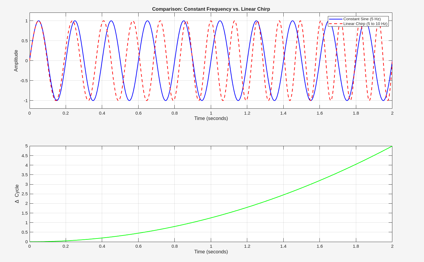
% 1. Define Parameters fs = 1000; % Sampling frequency (Hz) t = 0:1/fs:2; % Time vector (2 seconds duration)
f0 = 5; % Starting frequency for chirp / Frequency of constant sine (Hz) f1 = 10; % Ending frequency for chirp (Hz) T = max(t); % Total duration (seconds) k = (f1 - f0) / T; % Chirp rate (Hz/second)
% 2. Generate Signals y_constant = sin(2 * pi * f0 * t); % Constant frequency sine wave y_chirp = sin(2 * pi * f0 * t + pi * k * t.^2); % Linear chirp signal
dphi = pi * k * t.^2/2/pi;
% 3. Plot and Overlay Curves subplot(2,1,1) plot(t, y_constant, 'b-', 'LineWidth', 1.5); % Blue solid line for constant hold on; % Keep current plot to overlay next curve plot(t, y_chirp, 'r--', 'LineWidth', 1.5); % Red dashed line for chirp hold off; % Release the plot title('Comparison: Constant Frequency vs. Linear Chirp'); xlabel('Time (seconds)'); ylabel('Amplitude'); legend('Constant Sine (5 Hz)', 'Linear Chirp (5 to 10 Hz)', 'Location', 'northeast'); grid on; ylim([-1.21.2]);
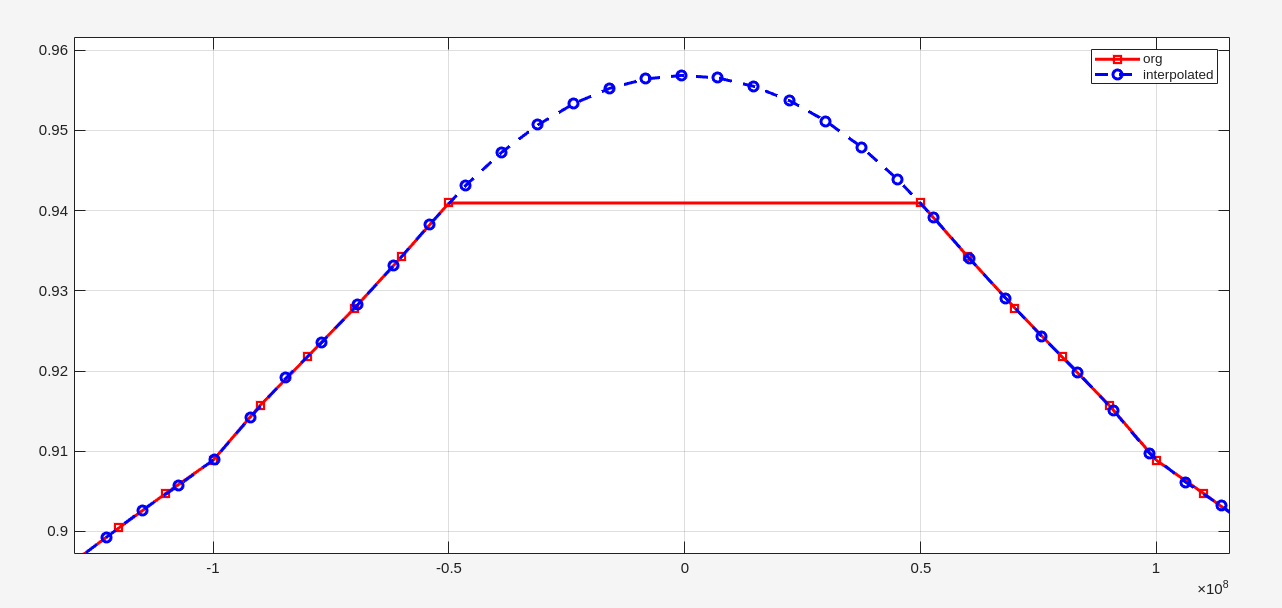
Hm_ds_interp=spline(fds_m,Hm_ds,f_ds_interp); % Interpolate for FFT point number figure(Name='spline function') plot(fds_m, Hm_ds, '-rs', LineWidth=2) hold on plot(f_ds_interp, Hm_ds_interp, '--bo', LineWidth=2) legend('org', 'interpolated'); grid on
impulse response from ifft of interpolated frequency
response
% Generate Random Data nt=1e3; %number of bits m=rand(1,nt+1); %random numbers between 1 and zero, will be quantized later m=-1*sign(m-0.5).^2+sign(m-0.5)+1;
% TX FIR Equalization Taps eq_taps=[1]; m_fir=filter(eq_taps,1,m);
for ( i=55:floor(size(data_channel,2) / bit_period)-500) eye_data(:,j) = 2*data_channel(floor((bit_period*(i-1)))+offset: floor((bit_period*(i+1)))+offset); j=j+1; end
time=0:2*bit_period; plot(time,eye_data);
If your 2D array represents multiple data series (e.g., each
column is a separate line seriessharing the same x-axis
values), the plot() function is the most
straightforward method.
% Take 10 pre-cursor, cursor, and 90 post-cursor samples sample_offset=opt_sample*bit_period; fori=1:101 sample_points(i)=max_data_ch_idx+sample_offset+(i-11)*bit_period; end sample_values=data_channel(sample_points); sample_points=(sample_points-max_data_ch_idx)./bit_period;
% Include DFE Equalization dfe_tap_num=2; dfe_taps(1:dfe_tap_num)=sample_values(12:12+dfe_tap_num-1); % h1, h2...
% Note this isn't a strtict DFE implementation - as I am not making a % decision on the incoming data. Rather, I am just using the known data % that I transmitted, delay matching this with the channel data, and using % it to subtract the ISI after weighting with the tap values. But, I think % it is good enough for these simulations. m_dfe=filter(dfe_taps,1,m); m_dfe_dr=reshape(repmat(m_dfe,bit_period,1),1,bit_period*size(m_dfe,2));
data_channel=data_channel'; dfe_fb_offset=floor(bit_period/2); % Point at which the DFE taps are subtracted - can be anything from 0 to UI-1*time_step data_channel_dfe=data_channel(channel_delay+dfe_fb_offset:channel_delay+dfe_fb_offset+size(m_dfe_dr,2)-1)-m_dfe_dr;
1 2 3 4 5 6 7
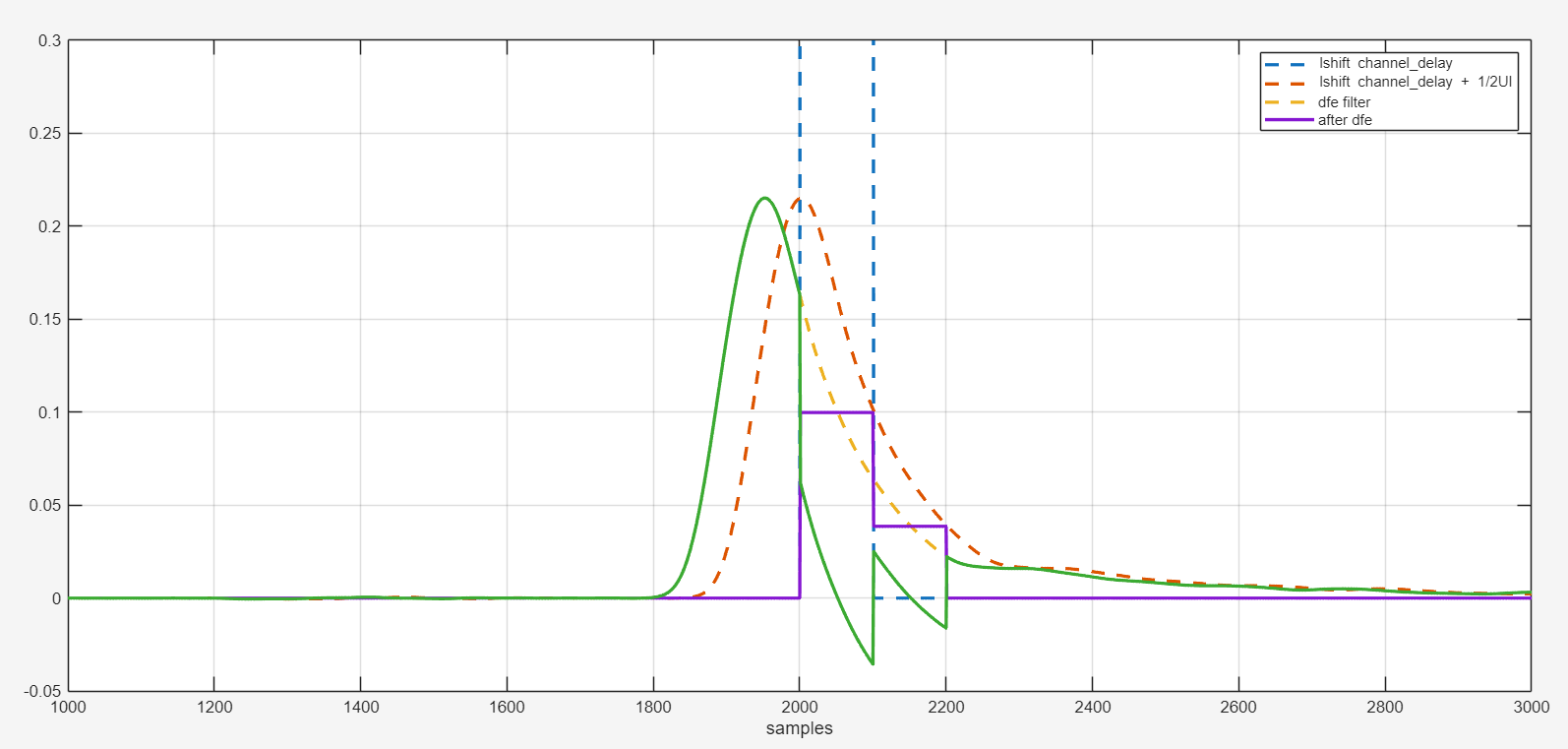
plot(m_dr, '--', LineWidth=2); hold on plot(data_channel(channel_delay:end), '--', LineWidth=2) hold on plot(data_channel(channel_delay+dfe_fb_offset:channel_delay+dfe_fb_offset+size(m_dfe_dr,2)-1), '--', LineWidth=2) plot(m_dfe_dr, LineWidth=2); plot(data_channel_dfe, LineWidth=2) xlim([1000, 3000]); ylim([-0.05, 0.3]); xlabel('samples'); grid on legend('lshift channel\_delay', 'lshift channel\_delay + 1/2UI', 'dfe filter', 'after dfe')
X. Chu, W. Guo, J. Wang, F. Wu, Y. Luo and Y. Li, "Fast and Accurate
Estimation of Statistical Eye Diagram for Nonlinear High-Speed Links,"
in IEEE Transactions on Very Large Scale Integration (VLSI) Systems,
vol. 29, no. 7, pp. 1370-1378, July 2021 [https://sci-hub.se/10.1109/TVLSI.2021.3082208]
IA Title: Common Electrical I/O (CEI) - Electrical and Jitter
Interoperability agreements for 6G+ bps, 11G+ bps, 25G+ bps I/O and 56G+
bps IA # OIF-CEI-04.0 December 29, 2017 [pdf]
J. Park and D. Kim, "Statistical Eye Diagrams for High-Speed
Interconnects of Packages: A Review," in IEEE Access, vol. 12,
pp. 22880-22891, 2024 [pdf]
StatOpt is a statistical eye
analysis and link optimization tool for
wireline communications, developed in both MATLAB and Python 3
The tool uses statistical methods to model various
wireline effects and to estimate the link performance metrics such as
the bit error rate and eye dimensions (eye's horizontal and vertical
openings)
High-Level Pipeline
flowchart TD
A["User Settings<br/>(GenerateUserSettingsExampleN)"] --> B["Settings Limits<br/>(GenerateSettingsLimits)"]
B --> C["Initialize Simulation<br/>(InitializeSimulation)"]
C --> D["Check Settings<br/>(CheckSettings)"]
D --> E["Fixed Influences<br/>(GenerateFixedInfluence)"]
E --> F{"Adaptation Loop<br/>while ~finished"}
F --> G["Variable Influences<br/>(GenerateVariableInfluence)"]
G --> H["Pulse Response<br/>(GeneratePulseResponse)"]
H --> I["ISI Trajectories<br/>(GenerateISI)"]
I --> J["PDF Eye Diagram<br/>(GeneratePDF)"]
J --> K["BER Contours<br/>(GenerateBER)"]
K --> L["Results / Measurements<br/>(GenerateResults)"]
L --> M["Adapt Link<br/>(AdaptLink)"]
M -->|not finished| F
M -->|finished| N["Display Plots<br/>(Display* functions)"]
Every function reads from and writes to two MATLAB structs that flow
through the entire pipeline:
Struct
Purpose
simSettings
All user-configurable knobs + derived constants. Populated once at
startup; mutated only by the adaptation engine.
simResults
Accumulates all computed data: channel responses, jitter/noise PDFs,
pulse responses, ISI trajectories, PDF/BER eye diagrams, measurements,
and adaptation state.
Computes channel and impairment data that does not
change across adaptation iterations:
flowchart LR
A["CreateChannel"] --> B["GenerateTXJitter"]
B --> C["GenerateTXDistortion"]
C --> D["GenerateRXJitter"]
D --> E["GenerateRXDistortion"]
E --> F["CombineInfluences"]
Variable Influences —
GenerateVariableInfluence.m
omputes impairment sources that depend on equalization
settings (and thus change during adaptation):
Sub-function
What it computes
GenerateCTLE
CTLE transfer function from zero/pole specs (cached to avoid
recomputation)
CalculateFFERMS
RMS of FFE tap values (needed for noise output-referring)
GenerateTXNoise
TX noise → attenuated through channel → amplified by CTLE/FFE →
Gaussian PDF at RX output
GenerateChannelNoise
Thermal noise → amplified by CTLE/FFE → Gaussian PDF
GenerateRXNoise
RX input-referred noise → amplified by pre-amp/CTLE/FFE → Gaussian
PDF
CombineInfluences
Convolves TX + channel + RX noise PDFs into total noise PDF
Noise is output-referred — each noise source is
propagated through the downstream signal chain (channel, CTLE, FFE)
before creating the probability distribution. This is why noise must be
recomputed when equalization changes.
Pulse Response —
GeneratePulseResponse.m
Builds the end-to-end pulse response through the full signal
chain:
flowchart LR
A["ApplyPulse<br/>(ideal pulse)"] --> B["ApplyTXEQ<br/>(FIR pre-emphasis)"]
B --> C["ApplyChannel<br/>(convolution with channel IR)"]
C --> D["ApplyRXGain<br/>(pre-amplifier)"]
D --> E["ApplyRXCTLE<br/>(continuous-time EQ via lsim)"]
E --> F["ApplyRXFFE<br/>(FIR equalization)"]
F --> G["ApplyRXDFE<br/>(post-cursor subtraction)"]
G --> H["LimitLength<br/>(trim to cursor window)"]
ISI Generation —
GenerateISI.m
Generates all possible signal trajectories due to inter-symbol
interference:
GenerateCursorCombinations — Enumerates all
M^N cursor patterns (M = modulation levels, N = cursor
count)
ClassifyTrajectories — Groups combinations by their
main-cursor transition type (e.g., trans01,
trans10)
SplitPulse — Slices the pulse response into
per-cursor segments
ApplyCursorCombination — For each combination,
multiplies cursors by data levels and sums → one trajectory per
combination
Computational complexity is O(M^N) — for PAM-4 with 7
cursors this is 4^7=16384 combinations. Reducing cursor
count speeds up simulation at the cost of accuracy
PDF Generation —
GeneratePDF.m
Builds the statistical eye diagram by layering impairments onto the
ISI distribution:
flowchart LR
A["GenerateHist<br/>(ISI → voltage histograms)"] --> B["ApplyCrossTalk<br/>(vertical convolution)"]
B --> C["ApplyDistortion<br/>(voltage remapping)"]
C --> D["ApplyJitter<br/>(horizontal convolution)"]
D --> E["ApplyNoise<br/>(vertical convolution)"]
E --> F["CombinePDFs<br/>(merge all transitions)"]
Each step creates a new named PDF layer (e.g.,
PDF.initial, PDF.crossTalk,
PDF.distorted, PDF.jitter,
PDF.noise, PDF.final), enabling intermediate
visualization.
Adaptation — AdaptLink.m
If simSettings.adaption.adapt = false, sets
finished = true and the loop exits after one pass.
If enabled, implements a genetic algorithm with
three modes:
flowchart LR
A["Mode 1: Coarse Search<br/>(±3 increments, N generations)"] --> B["Mode 2: Fine Search<br/>(±1 increment, N generations)"]
B --> C["Mode 3: Final Run<br/>(restore full settings, run optimal)"]
Seasim (Statistical Eye Analysis Simulator)
is a statistical channel simulation tool provided by
the PCI-SIG to help designers evaluate the signal integrity and
compliance of PCI Express (PCIe) links
other tools
IBIS-AMI
Init mode — Statistical (Fast) :
1 2 3 4 5 6 7
Channel ↓ Impulse response ↓ Compute DFE taps ↓ BER
GetWave mode Time-domain (Slow but more
realistic):
function int2bits(num, nbit) return [Bool((num>>k)%2) for k in nbit-1:-1:0] end
generate PAM symbols
here Big Endian
1 2 3 4 5
#generate PAM symbols fill!(So, zero(Float64)) #reset So to all 0 for n = 1:bits_per_sym @. So = So + 2^(bits_per_sym-n)*So_bits[n:bits_per_sym:end] end
1 2 3 4 5 6
function int2bits(num, nbit) return [Bool((num>>k)%2) for k in nbit-1:-1:0] end
FIR filter typically is much shorter (<10 taps) than the symbol
vector, using FFT convolution might be an overkill. For
optimization, a simple shift-and-add filter
function can be written
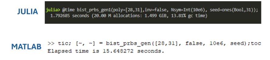
function bist_prbs_gen(;poly, inv, Nsym, seed) seq = Vector{Bool}(undef,Nsym) for n = 1:Nsym seq[n] = inv for p in poly seq[n] ⊻= seed[p] end seed .= [seq[n]; seed[1:end-1]] end return seq, seed end
1 2 3 4 5 6 7 8 9 10 11 12
%% Matlab
function[seq, seed] = bist_prbs_gen(poly,inv, Nsym, seed) seq = zeros(1,Nsym); for n = 1:Nsym seq(n) = inv; for p = poly seq(n) = xor(seq(n), seed(p)); end seed = [seq(n), seed(1:end-1)]; end end
Lim, Byong Chan, M. Horowitz, "Error Control and Limit Cycle
Elimination in Event-Driven Piecewise Linear Analog Functional Models,"
in IEEE Transactions on Circuits and Systems I: Regular Papers, vol. 63,
no. 1, pp. 23-33, Jan. 2016 [https://sci-hub.se/10.1109/TCSI.2015.2512699]
—, J. -E. Jang, J. Mao, J. Kim and M. Horowitz, "Digital Analog
Design: Enabling Mixed-Signal System Validation," in IEEE Design
& Test, vol. 32, no. 1, pp. 44-52, Feb. 2015 [http://iot.stanford.edu/pubs/lim-mixed-design15.pdf]
— , Mao, James & Horowitz, Mark & Jang, Ji-Eun & Kim,
Jaeha. (2015). Digital Analog Design: Enabling Mixed-Signal System
Validation. Design & Test, IEEE. 32. 44-52. [https://iot.stanford.edu/pubs/lim-mixed-design15.pdf]
S. Liao and M. Horowitz, "A Verilog piecewise-linear analog behavior
model for mixed-signal validation," Proceedings of the IEEE 2013
Custom Integrated Circuits Conference, San Jose, CA, USA, 2013 [https://sci-hub.se/10.1109/CICC.2013.6658461]
—, M. Horowitz, "A Verilog Piecewise-Linear Analog Behavior Model for
Mixed-Signal Validation," in IEEE Transactions on Circuits and
Systems I: Regular Papers, vol. 61, no. 8, pp. 2229-2235, Aug. 2014
[https://sci-hub.se/10.1109/TCSI.2014.2332265]
Ji-Eun Jang et al. “True event-driven simulation of
analog/mixed-signal behaviors in SystemVerilog: A decision-feedback
equalizing (DFE) receiver example”. In: Proceedings of the IEEE 2012
Custom Integrated Circuits Conference. 2012 [https://sci-hub.se/10.1109/CICC.2012.6330558]
—, Si-Jung Yang, and Jaeha Kim. “Event-driven simulation of Volterra
series models in SystemVerilog”. In: Proceedings of the IEEE 2013 Custom
Integrated Circuits Conference. 2013 [https://sci-hub.se/10.1109/CICC.2013.6658460]
T. Wen and T. Kwasniewski, "Phase Noise Simulation and Modeling of
ADPLL by SystemVerilog," 2008 IEEE International Behavioral Modeling
and Simulation Workshop, San Jose, CA, USA, 2008 [slides,
paper]
Jaeha Kim,Scientific Analog. UCIe PHY Modeling and Simulation with
XMODEL [pdf]
S. Katare, "Novel Framework for Modelling High Speed Interface Using
Python for Architecture Evaluation," 2020 IEEE REGION 10 CONFERENCE
(TENCON), Osaka, Japan, 2020 [https://sci-hub.se/10.1109/TENCON50793.2020.9293846]
Tianshuang Qiu; Ying Guo, "7. Finite-Precision Numerical Effects in
Digital Signal Processing," in Signal Processing and Data
Analysis , De Gruyter, 2018, pp.236-248
Antoniou, Andreas. “Digital Signal Processing: Signals, Systems, and
Filters.” (2005). [pdf]
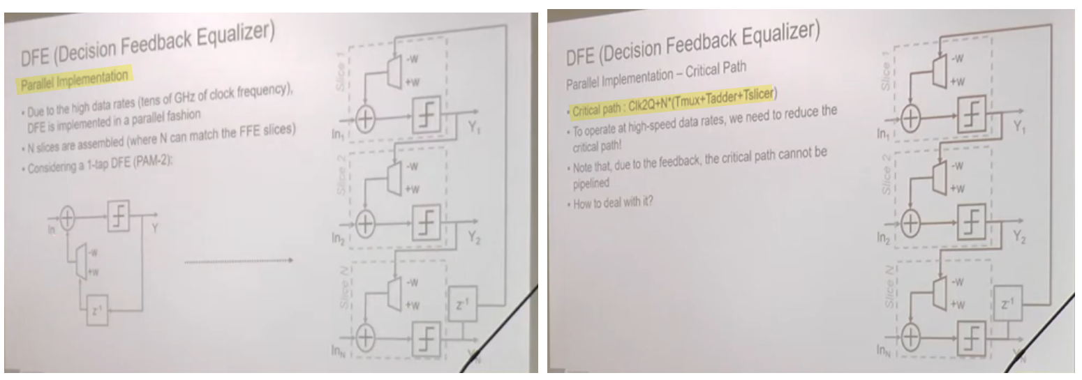
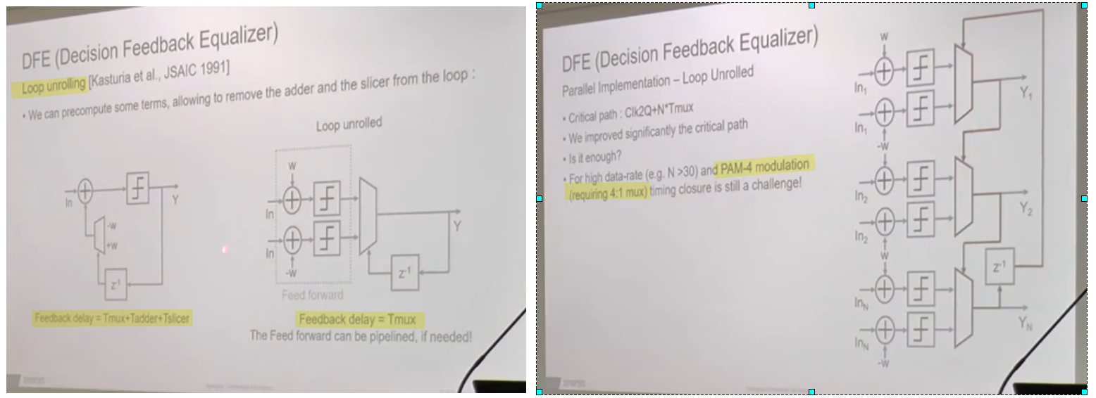
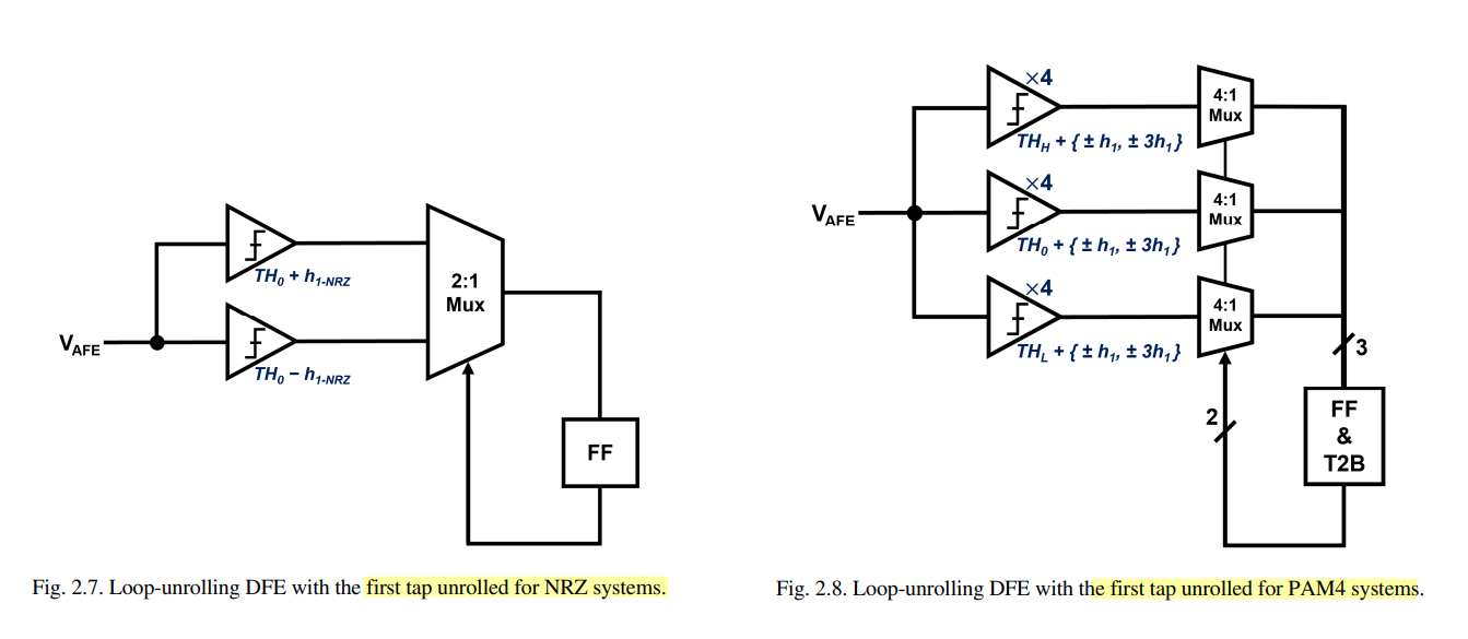
Corresponding to the three distinct voltage thresholds in the
PAM4 systems, it would need 12 slicers, 3
multiplexers, and one thermometer-to-binary decoder in
each deserialized data path, even if only one tap of the DFE is
unrolled
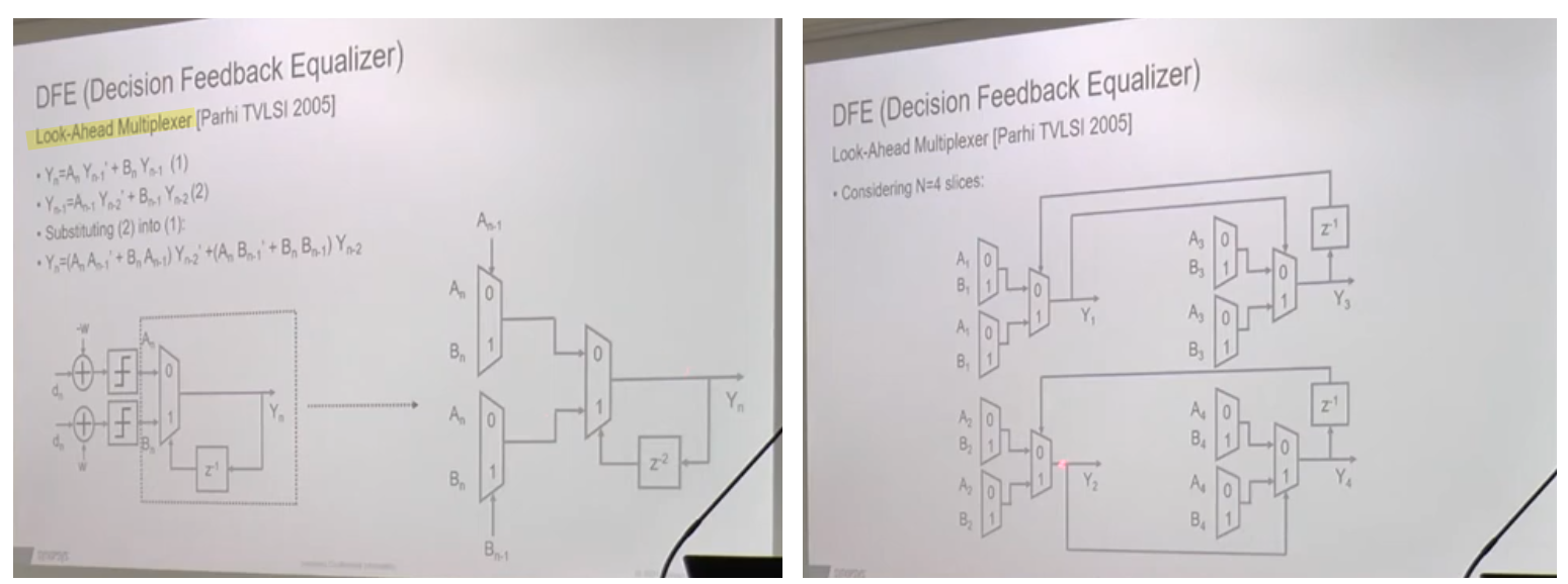
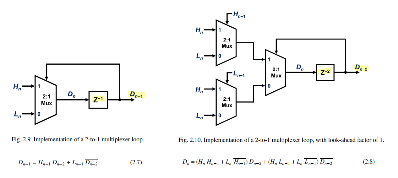
Look-Ahead Multiplexing DFE
The look-ahead multiplexing technique brings the key benefit that the
timing constraint can be significantly relaxed, as the iteration bound
is doubled at the expense of extra
hardware
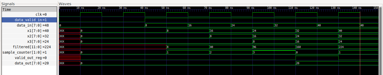
x1 <= data_in;   // line 34: scheduled, NOT applied yet
...
filtered = data_in + (x1<<1) + x1 + ...;  // line 37: x1 still holds OLD value
Non-blocking assignments don't take effect until the
end of the current time step (after all the blocking
statements in the block have run). So at line 37:
x1 still holds its previous value —
i.e. the sample from the lastdata_valid_in cycle,
which is x[n-1].
data_in is the current sample,
x[n].
They are different values. That's deliberate and necessary for the
FIR math to be correct:
A. Antoniou, "On the roots of digital signal processing. Part I," in
IEEE Circuits and Systems Magazine, vol. 7, no. 1, pp. 8-18,
First Quarter 2007
—, "Feature - On the roots of digital signal processing - Part II,"
in IEEE Circuits and Systems Magazine, vol. 7, no. 4, pp. 8-19,
Fourth Quarter 2007
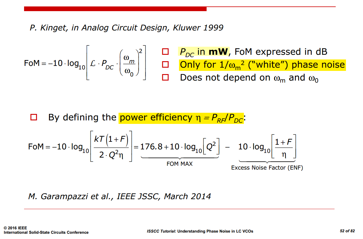
M. Garampazzi et al., "An Intuitive Analysis of Phase Noise
Fundamental Limits Suitable for Benchmarking LC Oscillators," in
IEEE Journal of Solid-State Circuits, vol. 49, no. 3, pp.
635-645, March 2014 [https://sci-hub.jp/10.1109/JSSC.2014.2301760]
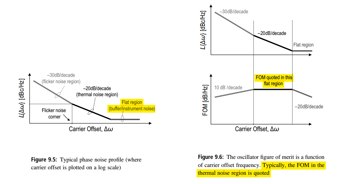
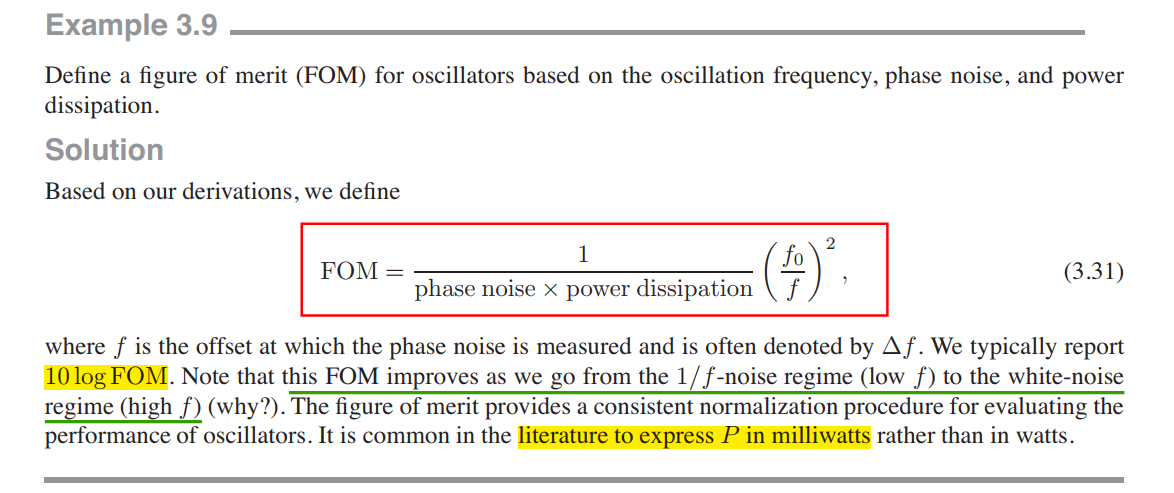
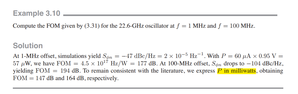
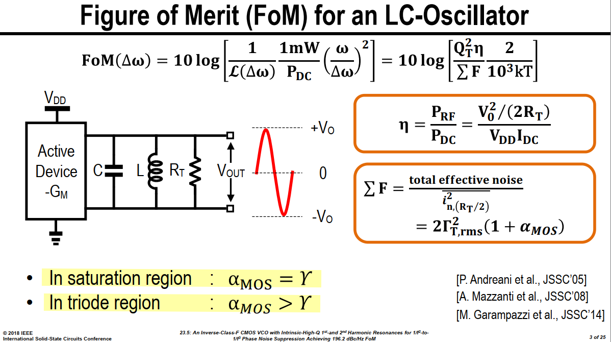
In general, FOM varies with carrier offset, but when reported as a
single number it is assumed that FOM was calculated
using measurements from the thermal noise region where
the FOM plateaus
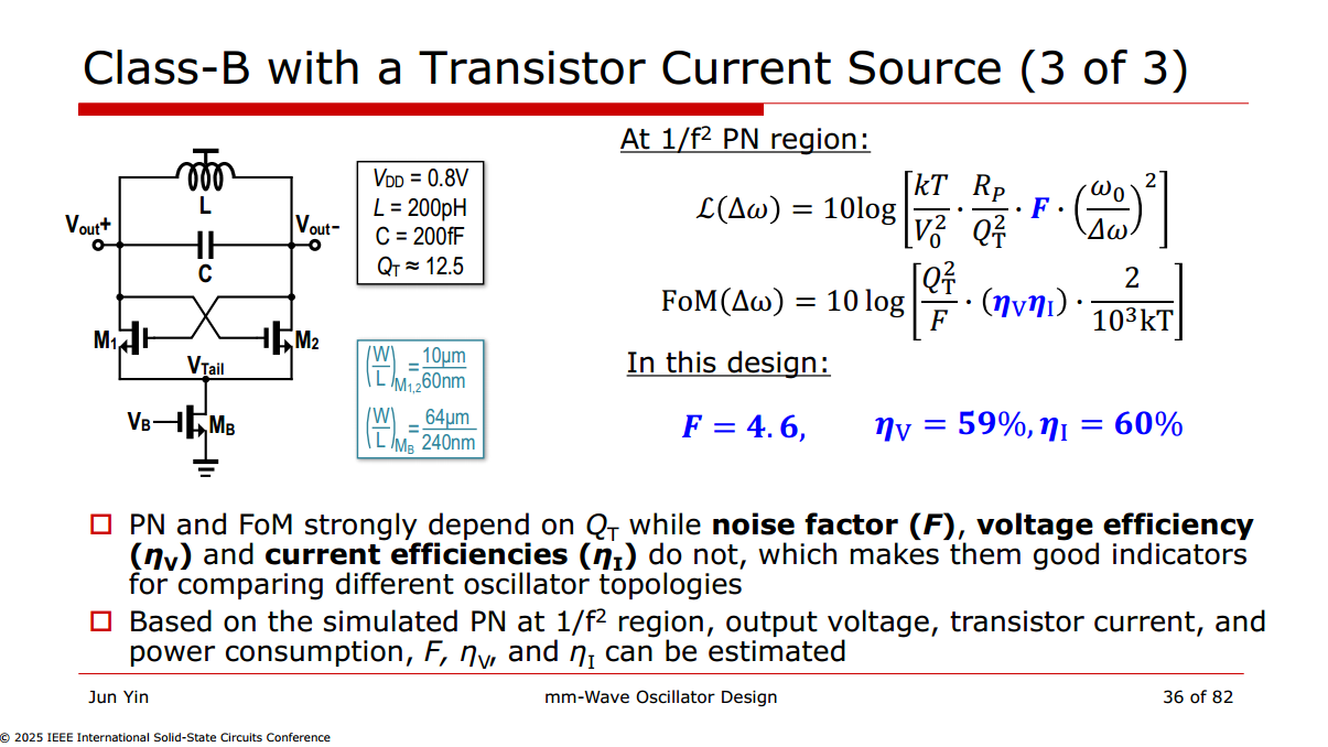
% noise factor by PN F = 10^(PN_1M/10)/(kB*T)/Rp/(f0/1e6)^2*V0^2*Qt^2; % 4.5960 % noise factor by FoM FF = Qt^2*eta_I*eta_V*2/1e3/(kB*T)/10^(FoM/10); % 4.6006
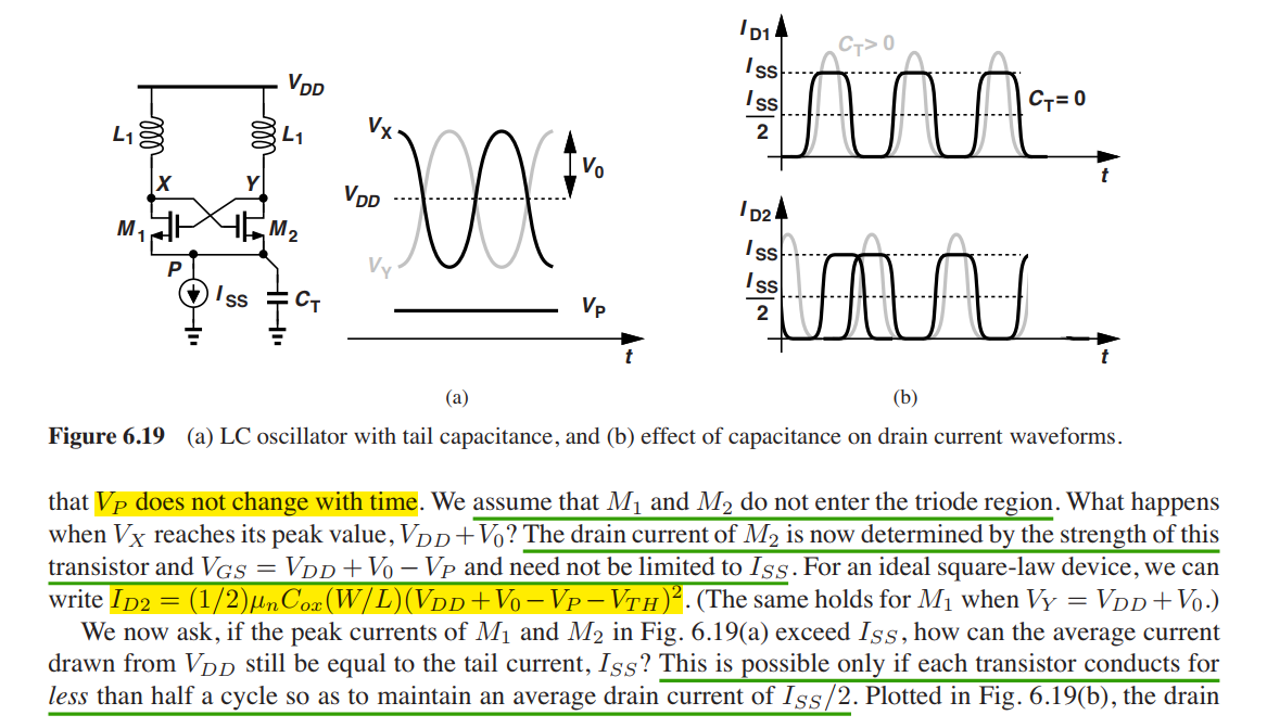
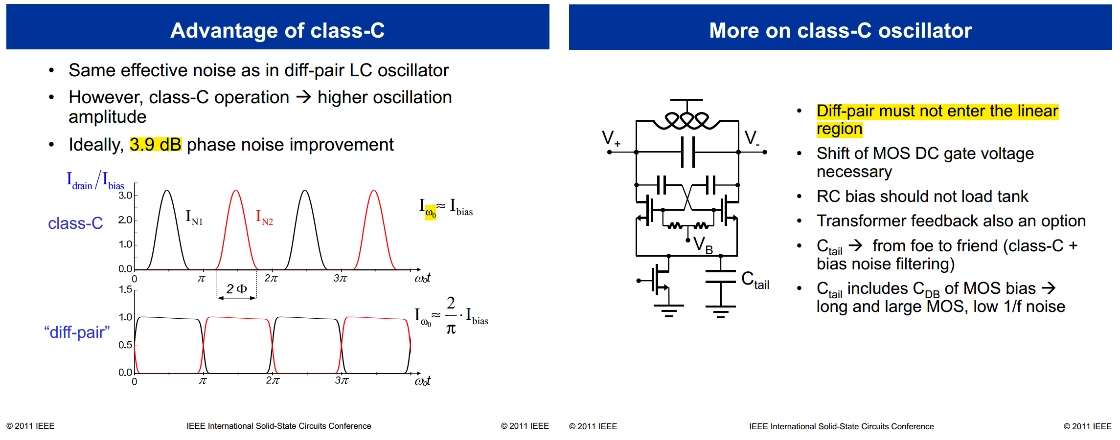
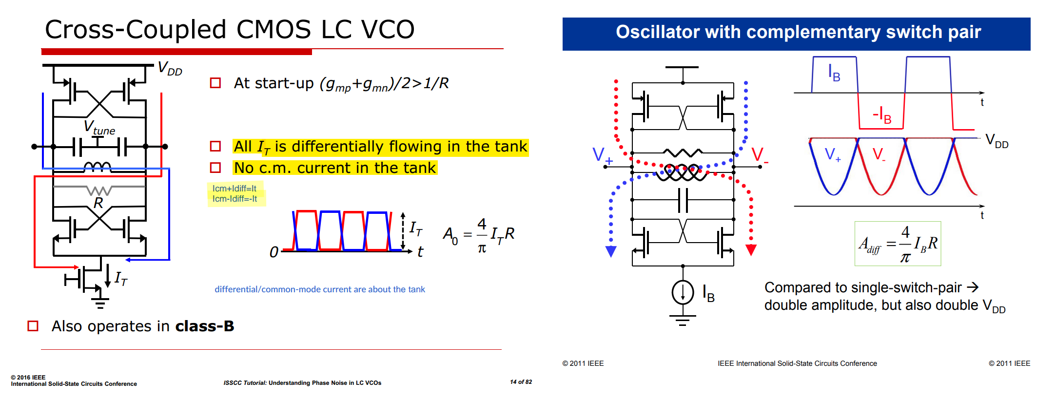
LC Oscillator Structures
Class-C / Tail
current-shaping CMOS Oscillator
B. Soltanian and P. Kinget, "A tail current-shaping technique to
reduce phase noise in LC VCOs," Proceedings of the IEEE 2005 Custom
Integrated Circuits Conference, 2005., San Jose, CA, USA, 2005 [https://sci-hub.ru/10.1109/CICC.2005.1568734]
—, "Tail Current-Shaping to Improve Phase Noise in LC
Voltage-Controlled Oscillators," in IEEE Journal of Solid-State
Circuits, vol. 41, no. 8, pp. 1792-1802, Aug. 2006 [https://sci-hub.ru/10.1109/JSSC.2006.877273]
A. Mazzanti and P. Andreani, "Class-C Harmonic CMOS VCOs, With a
General Result on Phase Noise," in IEEE Journal of Solid-State Circuits,
vol. 43, no. 12, pp. 2716-2729, Dec. 2008 [https://sci-hub.ru/10.1109/JSSC.2008.2004867]
TODO 📅
Class-D CMOS Oscillator
L. Fanori and P. Andreani, "A 2.5-to-3.3GHz CMOS Class-D VCO," 2013
IEEE International Solid-State Circuits Conference Digest of Technical
Papers, San Francisco, CA, USA, 2013 [https://sci-hub.red/10.1109/ISSCC.2013.6487763]
—, "A Class-D CMOS DCO with an on-chip LDO," ESSCIRC 2014 - 40th
European Solid State Circuits Conference (ESSCIRC), Venice Lido, Italy,
2014 [https://sci-hub.red/10.1109/ESSCIRC.2014.6942090]
TODO 📅
Class-B
Class-D
oscillation amplitude
Idd & LC-tank losses
VDD
current consumption
VDD & LC-tank losses
Class-F CMOS Oscillator
Huijung Kim, Seonghan Ryu, Yujin Chung, Jinsung Choi and Bumman Kim,
"A low phase-noise CMOS VCO with harmonic tuned LC tank," in IEEE
Transactions on Microwave Theory and Techniques, vol. 54, no. 7, pp.
2917-2924, July 2006 [https://sci-hub.ru/10.1109/tmtt.2006.877439]
M. Babaie and R. B. Staszewski, "Third-harmonic injection technique
applied to a 5.87-to-7.56GHz 65nm CMOS Class-F oscillator with 192dBc/Hz
FOM," 2013 IEEE International Solid-State Circuits Conference Digest of
Technical Papers, San Francisco, CA, USA, 2013 [https://sci-hub.ru/10.1109/ISSCC.2013.6487764]
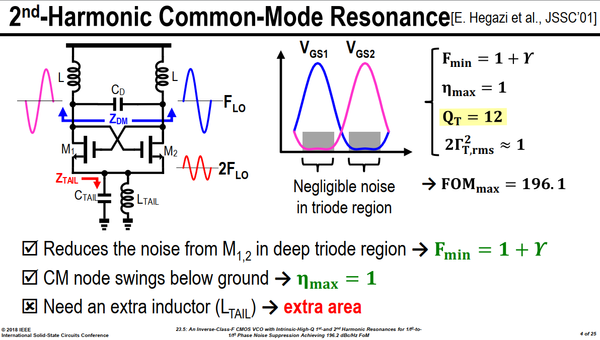
C. -C. Lim, J. Yin, P. -I. Mak, H. Ramiah and R. P. Martins, "An
inverse-class-F CMOS VCO with intrinsic-high-Q 1st- and 2nd-harmonic
resonances for 1/f2-to-1/f3 phase-noise suppression achieving
196.2dBc/Hz FOM," 2018 IEEE International Solid-State Circuits
Conference - (ISSCC), San Francisco, CA, USA, 2018 [paper]
—, "An Inverse-Class-F CMOS Oscillator With Intrinsic-High-Q First
Harmonic and Second Harmonic Resonances," in IEEE Journal of
Solid-State Circuits, vol. 53, no. 12, pp. 3528-3539, Dec. 2018 [https://sci-hub.jp/10.1109/JSSC.2018.2875099]
X. Meng, H. Li, P. Chen, J. Yin, P. -I. Mak and R. P. Martins,
"Analysis and Design of a 15.2-to-18.2-GHz Inverse-Class-F VCO With a
Balanced Dual-Core Topology Suppressing the Flicker Noise Upconversion,"
in IEEE Transactions on Circuits and Systems I: Regular Papers,
vol. 70, no. 12, pp. 5110-5123, Dec. 2023
TODO 📅
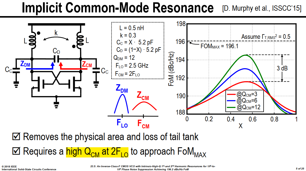
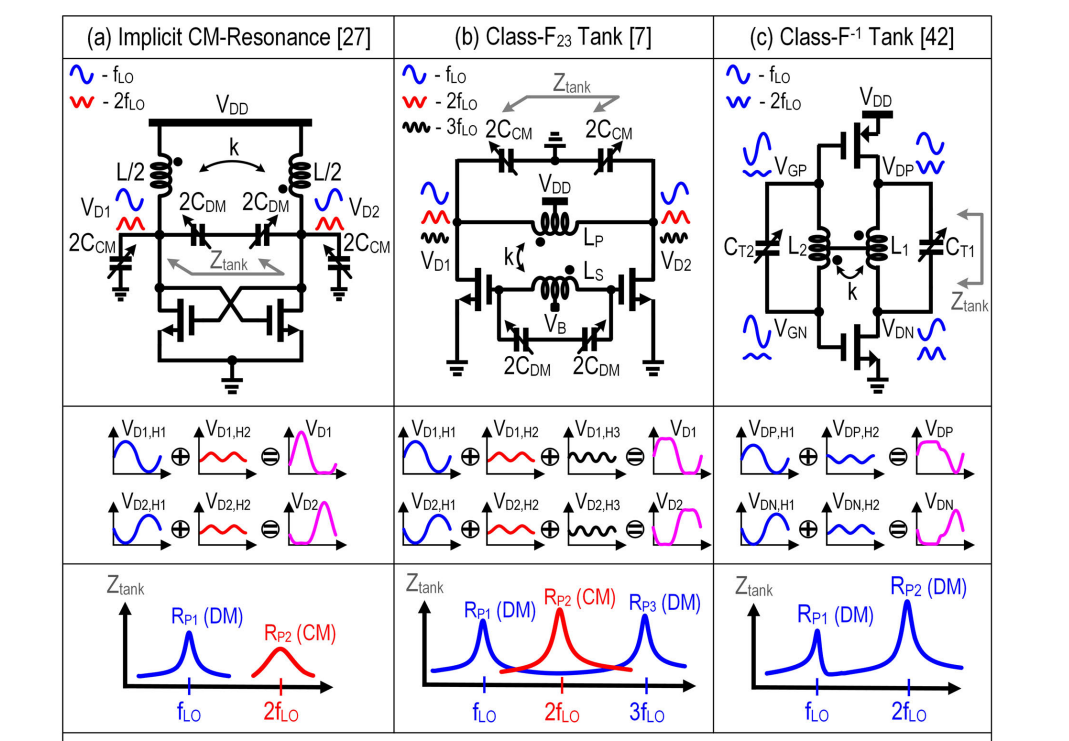
Higher \(Q_\text{CM}\) is preferred
for better FoM
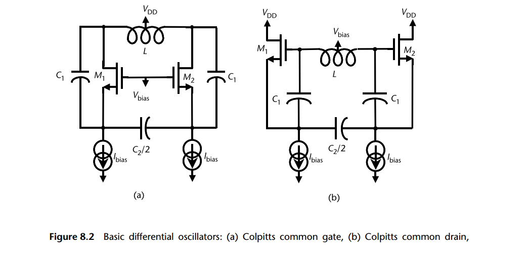
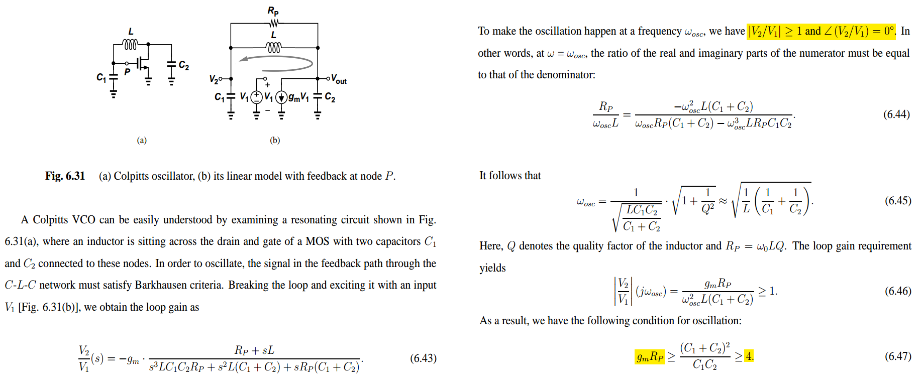
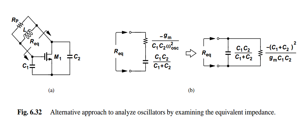
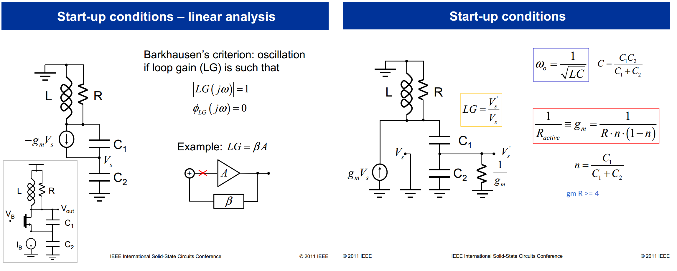
Colpitts oscillator
John Rogers, Calvin Plett, and Foster Dai. 2006. Integrated Circuit
Design for High-Speed Frequency Synthesis (Artech House Microwave
Library). Artech House, Inc., USA.
This type of oscillator could be operated with only one
transistor. In modern times, the abundance of transistors and
the desire for differential circuits favors a symmetric Colpitts
oscillators
common-source Colpitts
common-gate Colpitts
TODO 📅
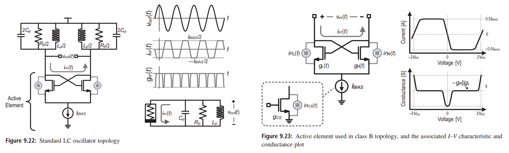
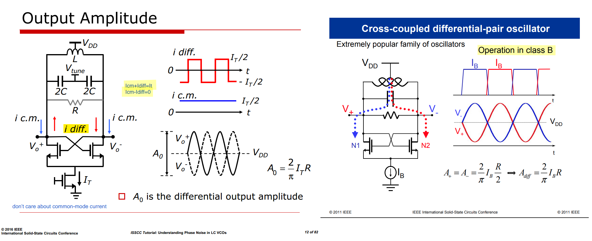
Class-B Oscillators
active element provides a negative conductance only when the input
voltage is small
For larger voltages, one of the transistors in the differential pair
will be off, while the other will be on, and the conductance drops to
zero
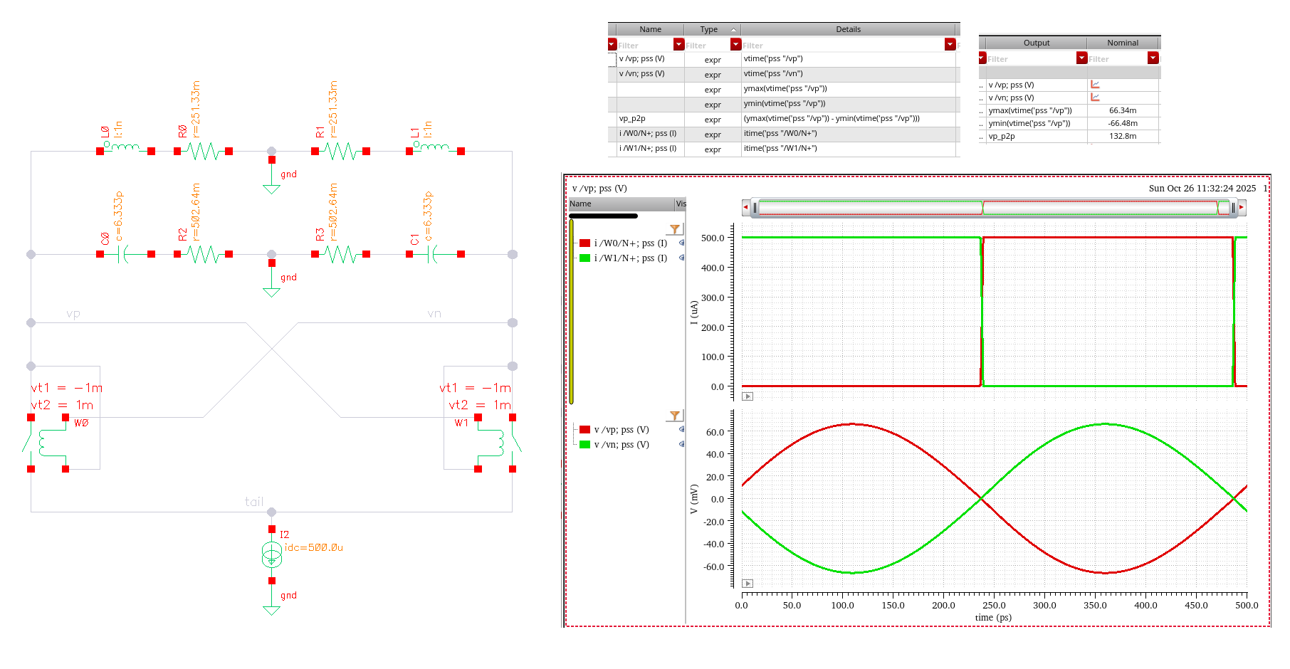
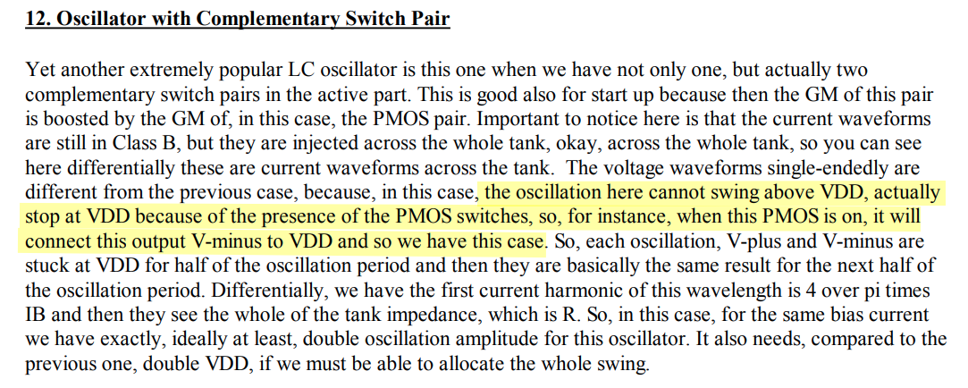
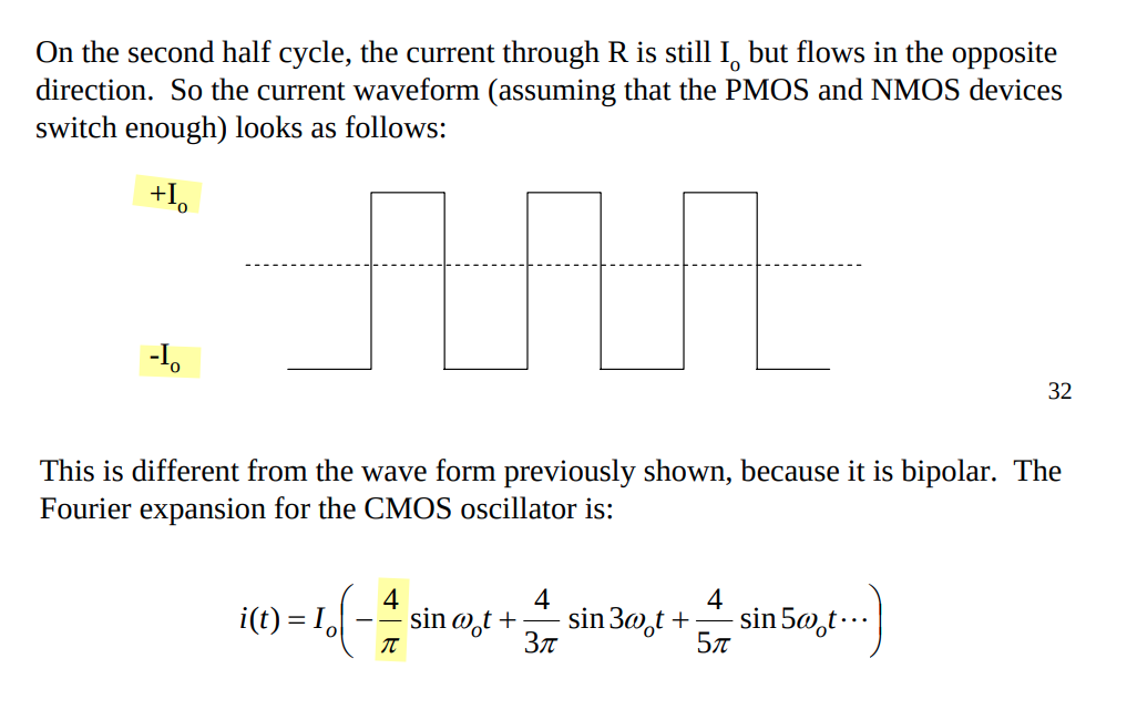
Owing to switch-off PMOS eliminating common mode current, all \(I_T\) is differentially flowing in the
tank
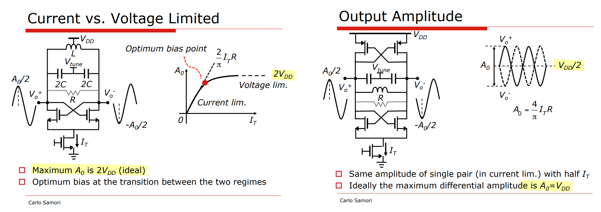
current limited vs voltage limited
Class-B Power/Current
Efficiency
Z. Wang, S. Diao, L. He, X. Jiang and F. Lin, "Analysis of Current
Efficiency for CMOS Class-B LC Oscillators," in IEEE Transactions on
Circuits and Systems I: Regular Papers, vol. 62, no. 5, pp.
1345-1352, May 2015 [https://sci-hub.jp/10.1109/TCSI.2015.2411792]
L. Bertulessi, S. Levantino and C. Samori, "Analysis of power
efficiency in high-performance class-B oscillators," 2016 12th
Conference on Ph.D. Research in Microelectronics and Electronics
(PRIME), Lisbon, Portugal, 2016 [https://sci-hub.jp/10.1109/PRIME.2016.7519525]
TODO 📅
Current-biased &
voltage-biased
S. Gallucci et al., "A Low-Noise Digital PLL With an
Adaptive Common-Mode Resonance Tuning Technique for Voltage-Biased
Oscillators," in IEEE Journal of Solid-State Circuits, vol. 60,
no. 12, pp. 4572-4586, Dec. 2025
TODO 📅
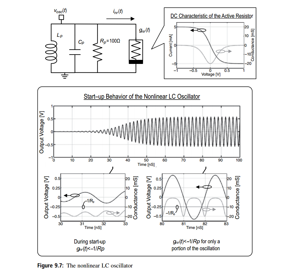
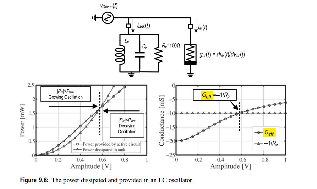
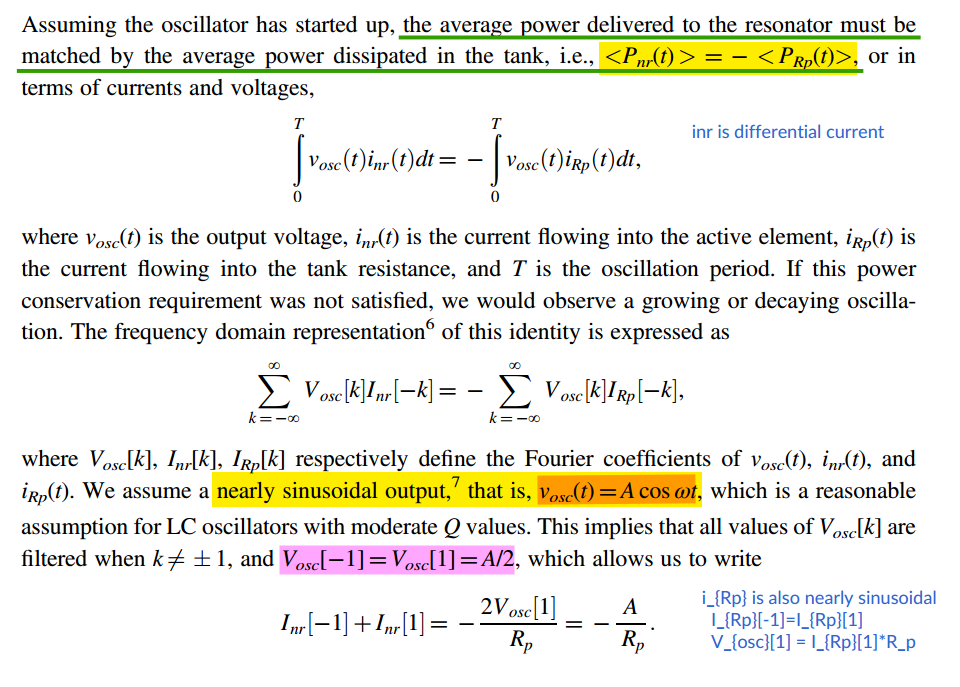
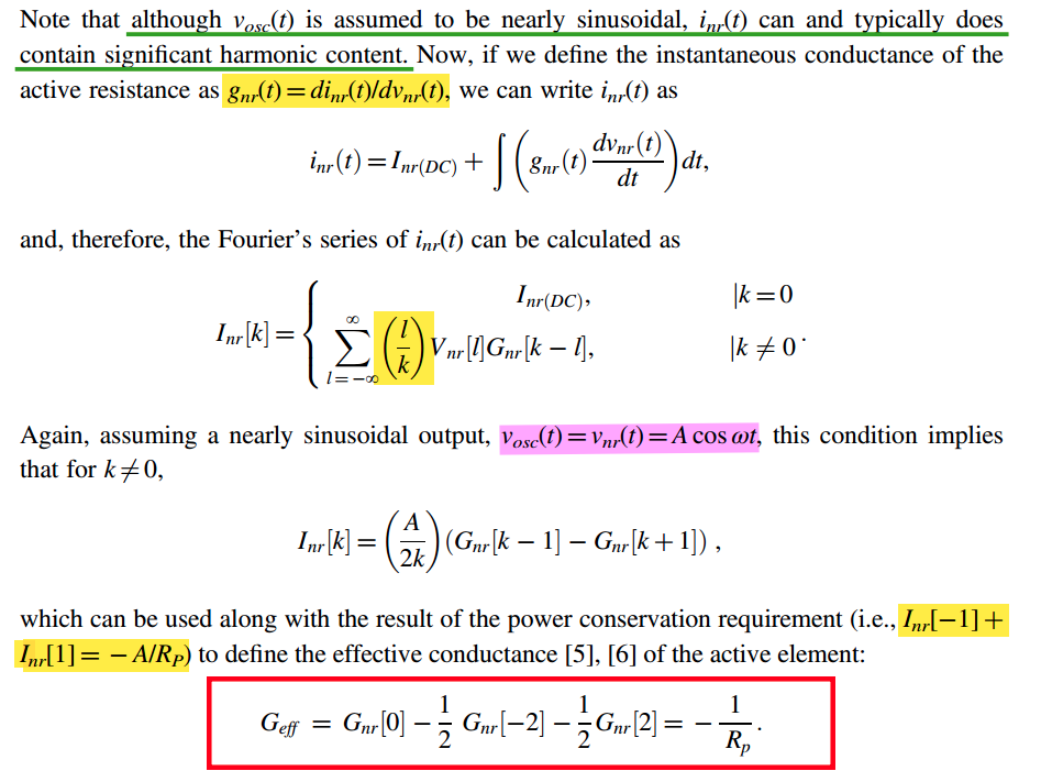
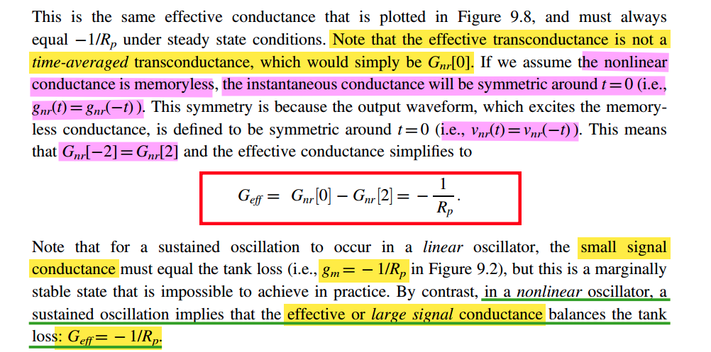
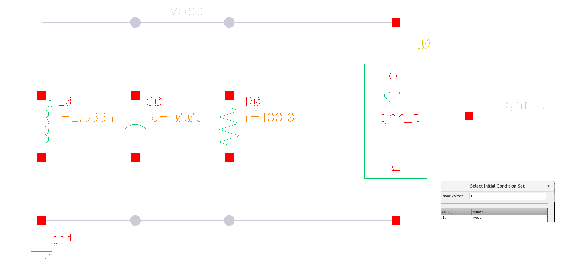
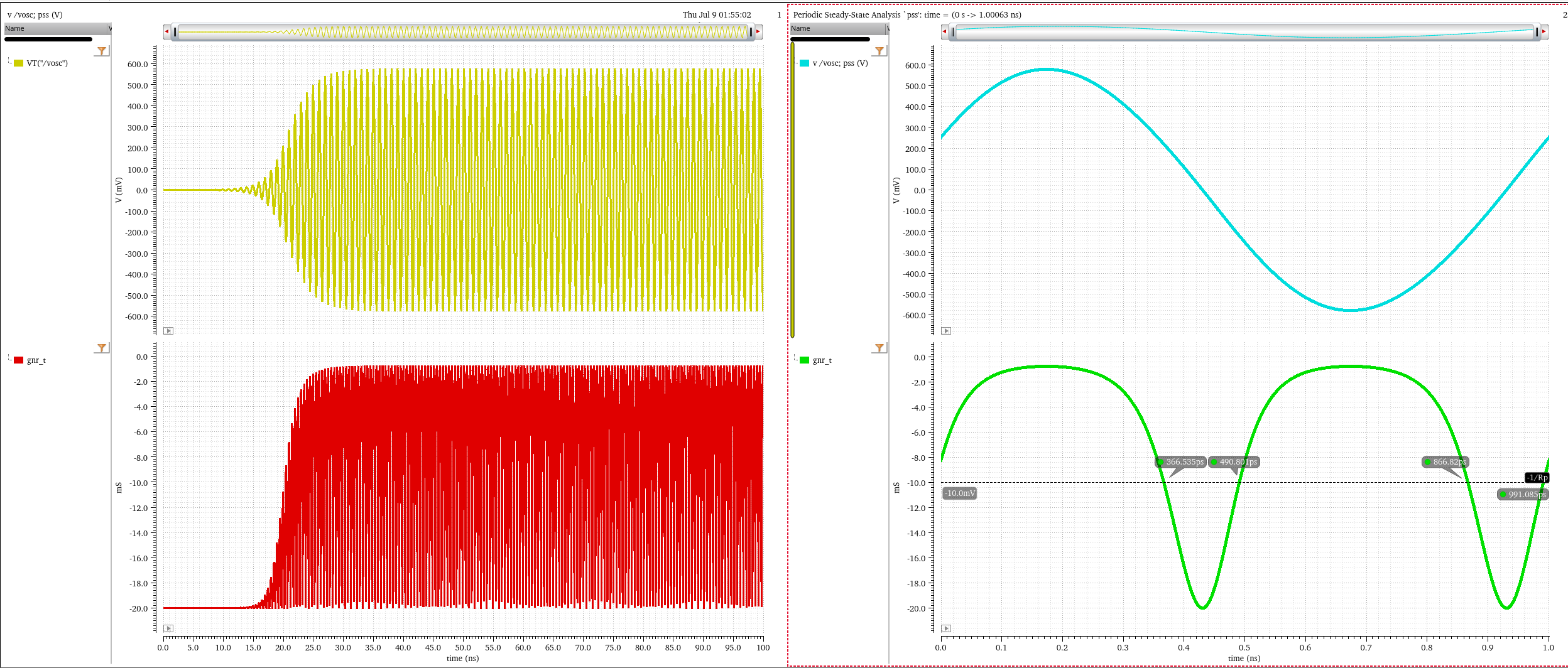
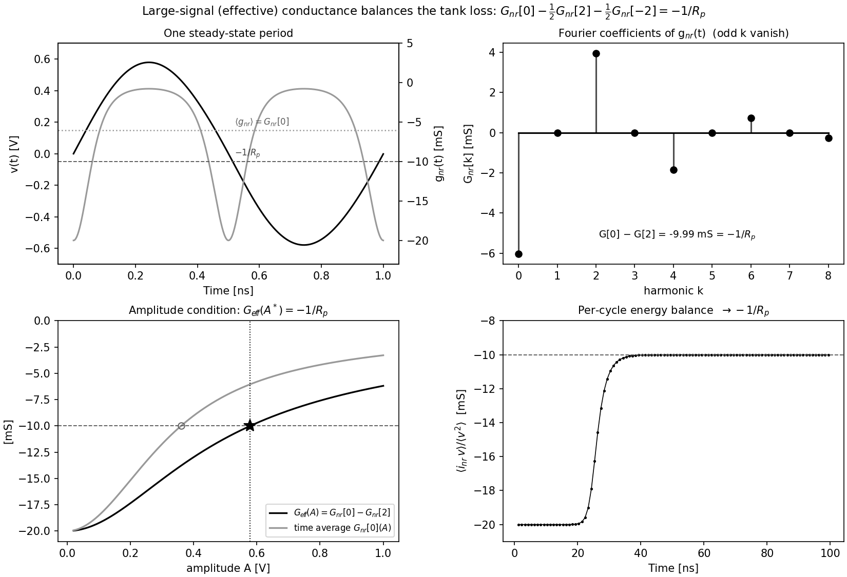
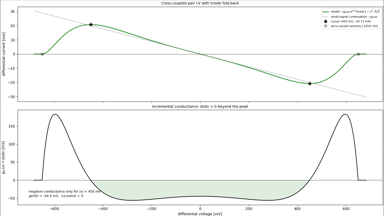
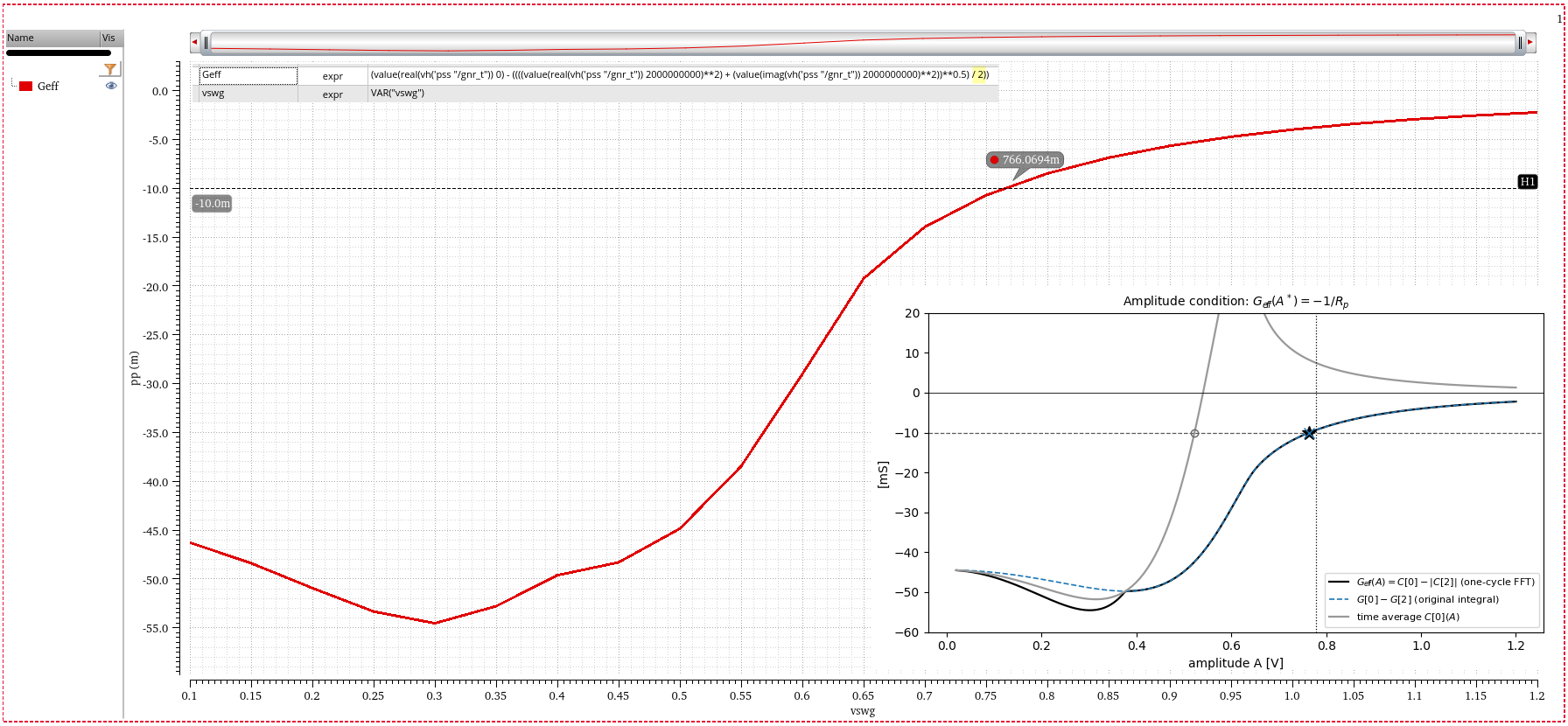
Startup & Geff
effective or large signal conductance
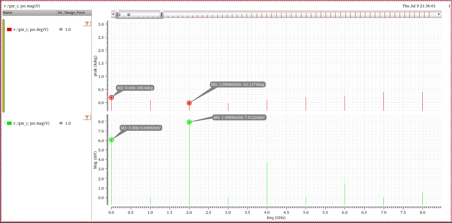
Note that the gnr frequency is twice of oscillator voltage
frequency
Power Conservation Requirements
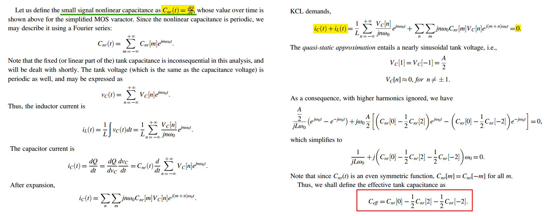
Since the Fourier transform of a real and even function is also real
and even, the derivation above assumes that \(V_{\text{osc}}(t)\) is real and even, which
implies that \(g_{\text{nr}}(t)\) is likewise real and
even — \(G_\text{nr}\) is
real and even
For a symmetric signal \(g_\text{nr}(t)\), the phase angle \(\theta\) is absorbed into the phase shift,
transforming the second-harmonic component as: \[
h_{2}(t)=\mathcal{Re}\{2Ae^{j(2\omega _{0}t+\theta )}\}\rightarrow
h_{2}(t)=2A\cos (2\omega _{0}t)
\]
This yields \(G_\text{nr}[2] =
G_\text{nr}[-2] = A = 3.956\). Consequently, the effective gain
is evaluated as: \[
G_{\text{eff}}=G_{\text{nr}}[0]-G_{\text{nr}}[2]=-9.9968 \approx
-\frac{1}{R_p}
\]
Because the magnitude of \(G_\text{nr}[2]\) is comparable to that of
\(G_\text{nr}[0]\), \(G_\text{nr}[2]\) must be retained
E. Hegazi and A. A. Abidi, "Varactor characteristics, oscillator
tuning curves, and AM-FM conversion," in IEEE Journal of Solid-State
Circuits, vol. 38, no. 6, pp. 1033-1039, June 2003 [https://sci-hub.jp/10.1109/JSSC.2003.811968]
TODO 📅
\[
\boxed{\oint i_{nr}\,dv_{nr}
=
\int_0^T i_{nr}(t)\frac{dv_{nr}(t)}{dt}\,dt}
\] It is the signed area-related quantity swept
in the \(i\)-\(v\) plane over one period,
which is used as a memory detector — a one-line mathematical
test for whether an element's behavior depends on its history
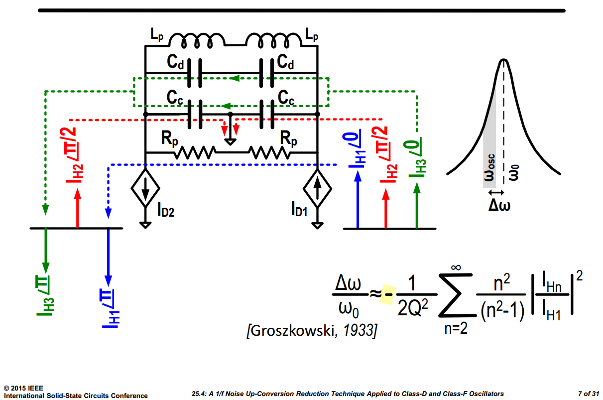
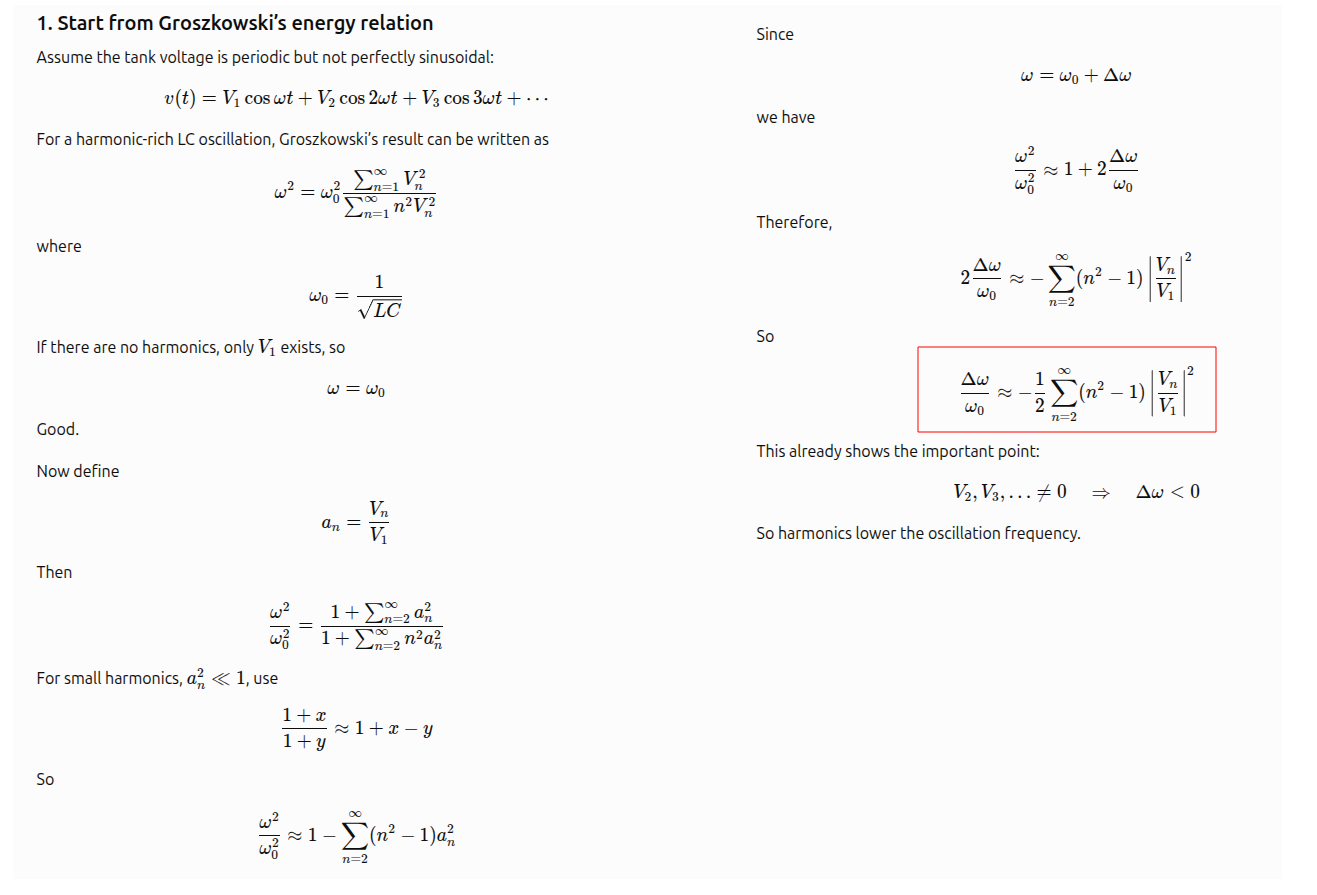
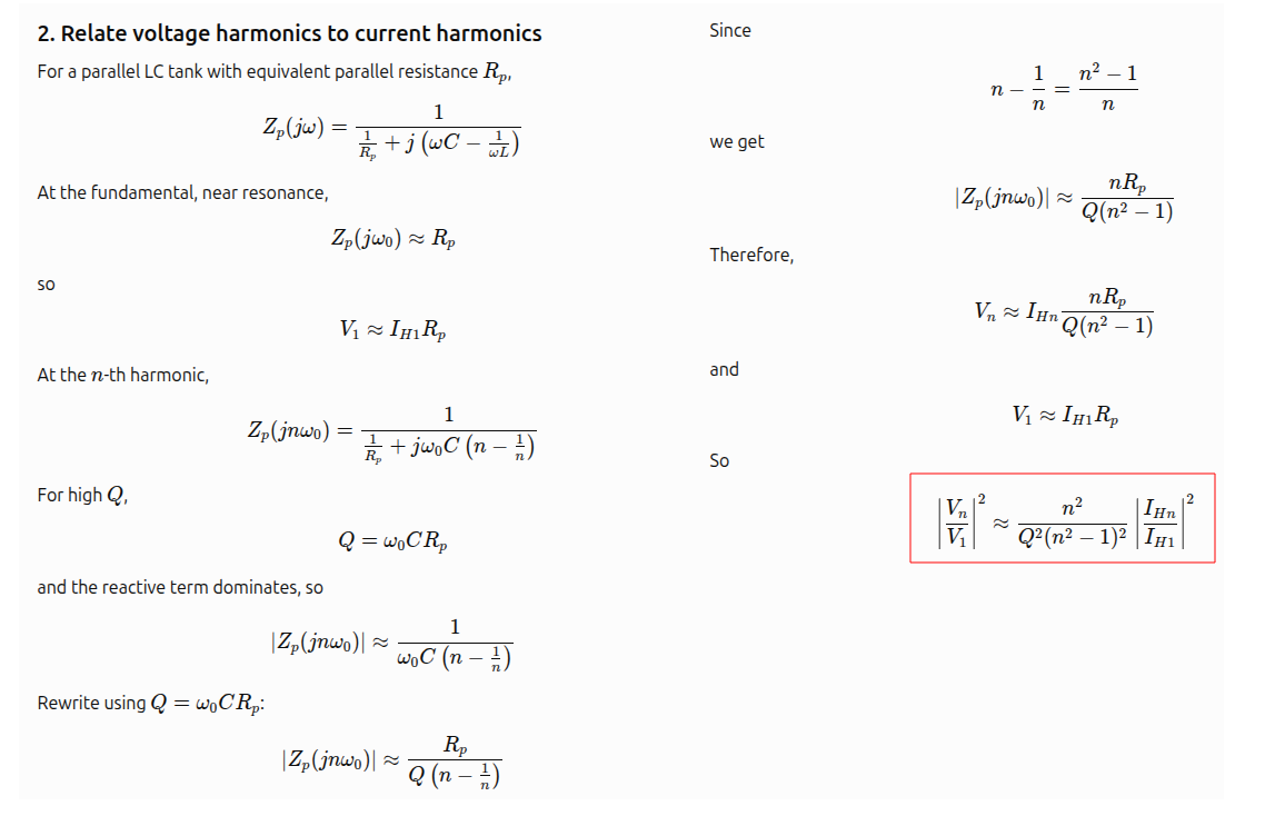
Groszkowski's Effect
indirect injection of flicker noise from the tail current source was
analyzed by "Groszkowski effect" (different from the ISF theory).
However it fails to explain the \(1/f\) noise upconversion from the
cross-coupled pair
The Groszkowski effect relies on AM-to-FM conversion:
nonlinearities make the oscillation frequency
amplitude-dependent, so amplitude fluctuations are converted into
frequency fluctuation
\[
\delta \omega
=
\frac{\partial \omega_0}{\partial A}\,
\delta A.
\]
Thus, the flicker noise from the tail current source is converted
into phase noise through the following sequence:
Unlike the Groszkowski effect, this mechanism does not rely
on amplitude-to-frequency conversion
credits to GPT-5.5 High
Groszkowski's effect is an oscillator
frequency shift caused by harmonic content in the
oscillation waveform/current
For a periodic LC oscillation, the average
stored energy must balance between \(C\) and \(L\)
average energy balance\(\overline{W_L}=\overline{W_C}\), or
equivalently \[
\sum L I_n^2 = \sum C V_n^2
\]\(I_n\) here is the
reactive tank current harmonic, not directly the
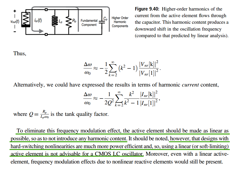
transistor current harmonic \(I_{Hn}\)
in the slide
P. Guan et al., "8-Shaped Inductors: An Essential Addition to RFIC
Designers' Toolbox," in IEEE Open Journal of the Solid-State Circuits
Society, vol. 4, pp. 131-146, 2024 [pdf]
M. Pisati et al., "A 243-mW 1.25–56-Gb/s Continuous Range PAM-4
42.5-dB IL ADC/DAC-Based Transceiver in 7-nm FinFET," in IEEE Journal of
Solid-State Circuits, vol. 55, no. 1, pp. 6-18, Jan. 2020 [https://sci-hub.ru/10.1109/JSSC.2019.2936307]
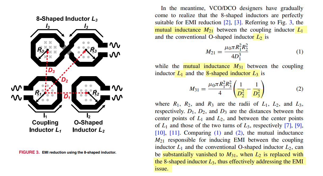
An 8-shaped (figure-8) inductor is a specialized
on-chip, high-Q component used to mitigate electromagnetic
coupling and reduce frequency pulling in VCOs
by generating opposing, self-canceling magnetic fields
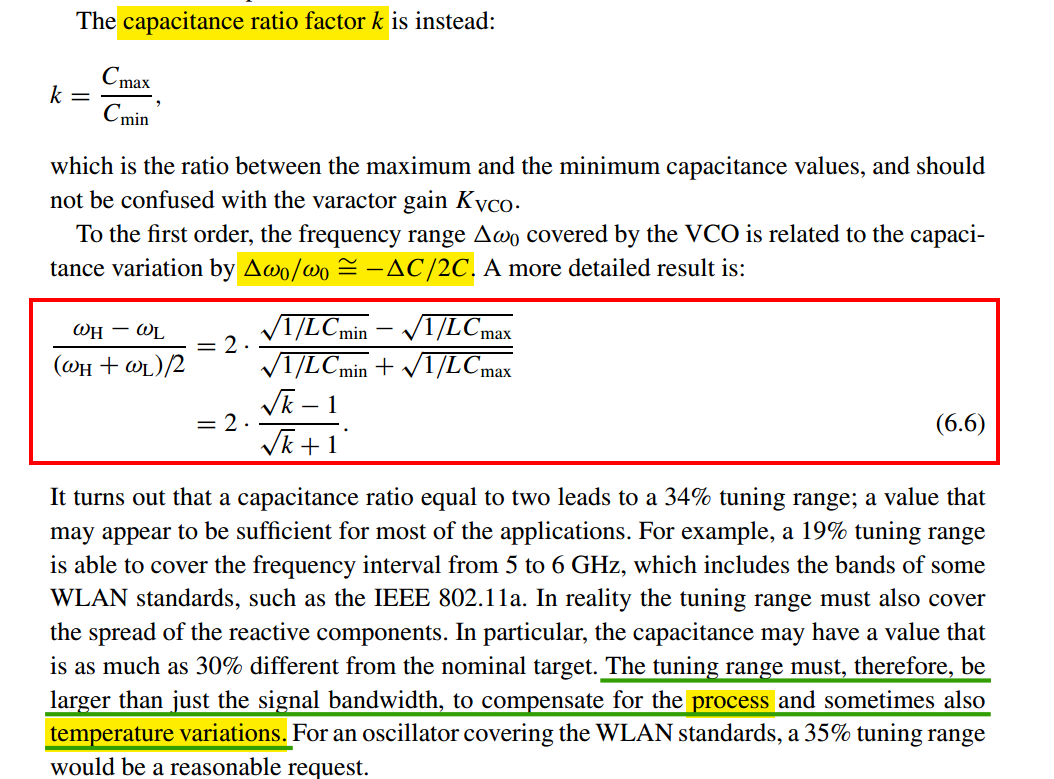
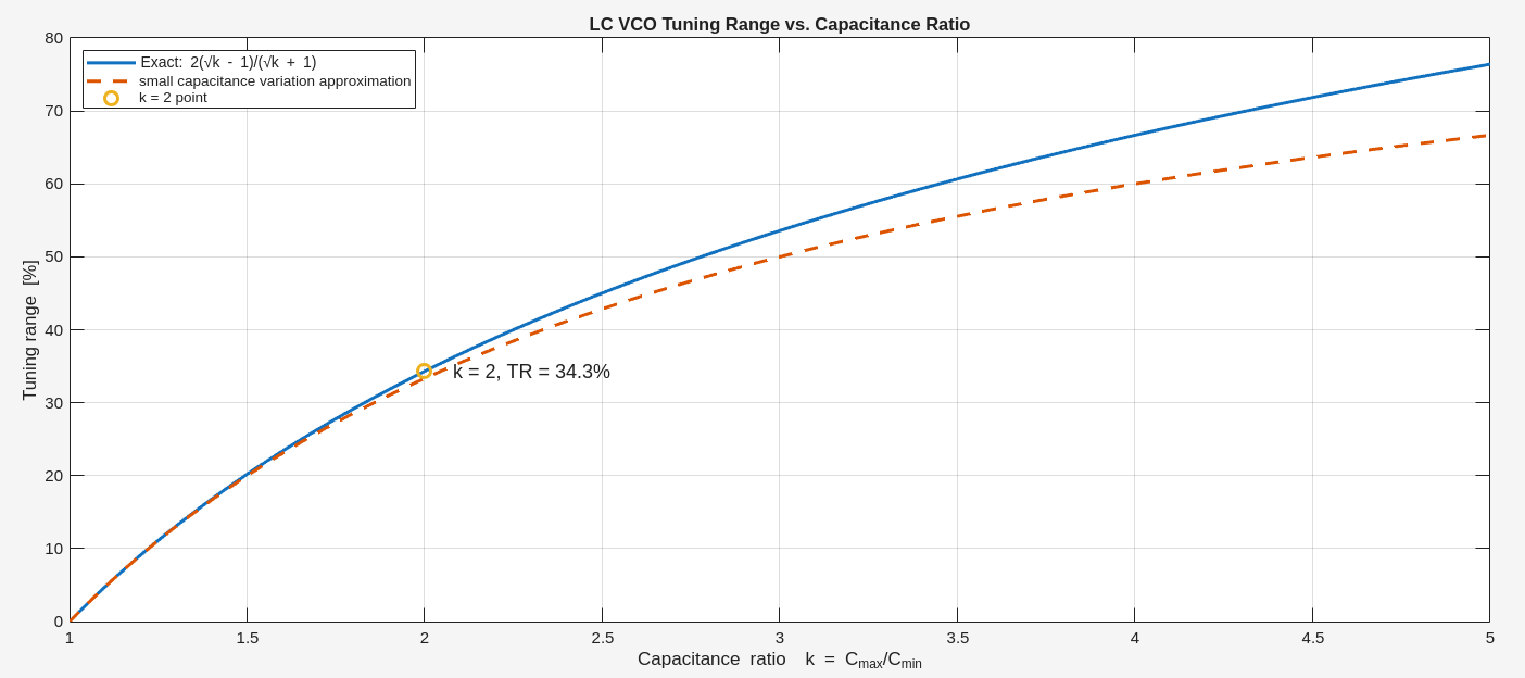
characterized by by quality factor and
capacitance ratio factor
tuning range
\[
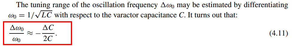
\Delta\omega_0 = \frac{\partial \omega_0}{\partial C}\cdot \Delta C =
-\frac{\Delta C}{2C}\cdot \omega_0
\] For tuning range, use the magnitude: \[
TR_{\text{approx}}
\approx
\frac{1}{2}\frac{C_{\max}-C_{\min}}{C_{\text{avg}}}
\] where \(C_{\text{avg}}=\frac{C_{\max}+C_{\min}}{2}\)
Therefore: \[
TR_{\text{approx}}
\approx
\frac{1}{2}
\frac{C_{\max}-C_{\min}}
{(C_{\max}+C_{\min})/2}
\] Now divide numerator and denominator by \(C_{\min}\): \[
TR_{\text{approx}}
=
\frac{C_{\max}/C_{\min}-1}
{C_{\max}/C_{\min}+1}
\] Since \(k=\frac{C_{\max}}{C_{\min}}\)
we get \[
\boxed{
TR_{\text{approx}}
=
\frac{k-1}{k+1}
}
\]
capacitance ratio factor
quality factor
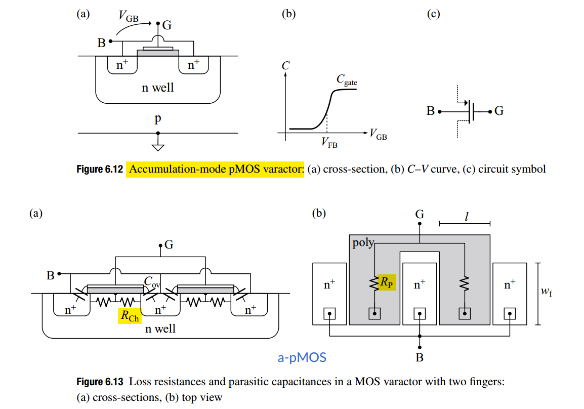
Two resistances, both in series with the variable capacitance:
RCh is the channel
resistance of the accumulation layer
RP is the gate
resistance due to the finite polysilicon conductivity
Capacitor Bank
B. Sadhu and R. Harjani, "Capacitor bank design for wide tuning range
LC VCOs: 850MHz-7.1GHz (157%)," Proceedings of 2010 IEEE International
Symposium on Circuits and Systems, Paris, France, 2010 [https://sci-hub.st/10.1109/ISCAS.2010.5537040]
TODO 📅
large value KVCO is not favorable due to noise and possibly spurs at
the control voltage
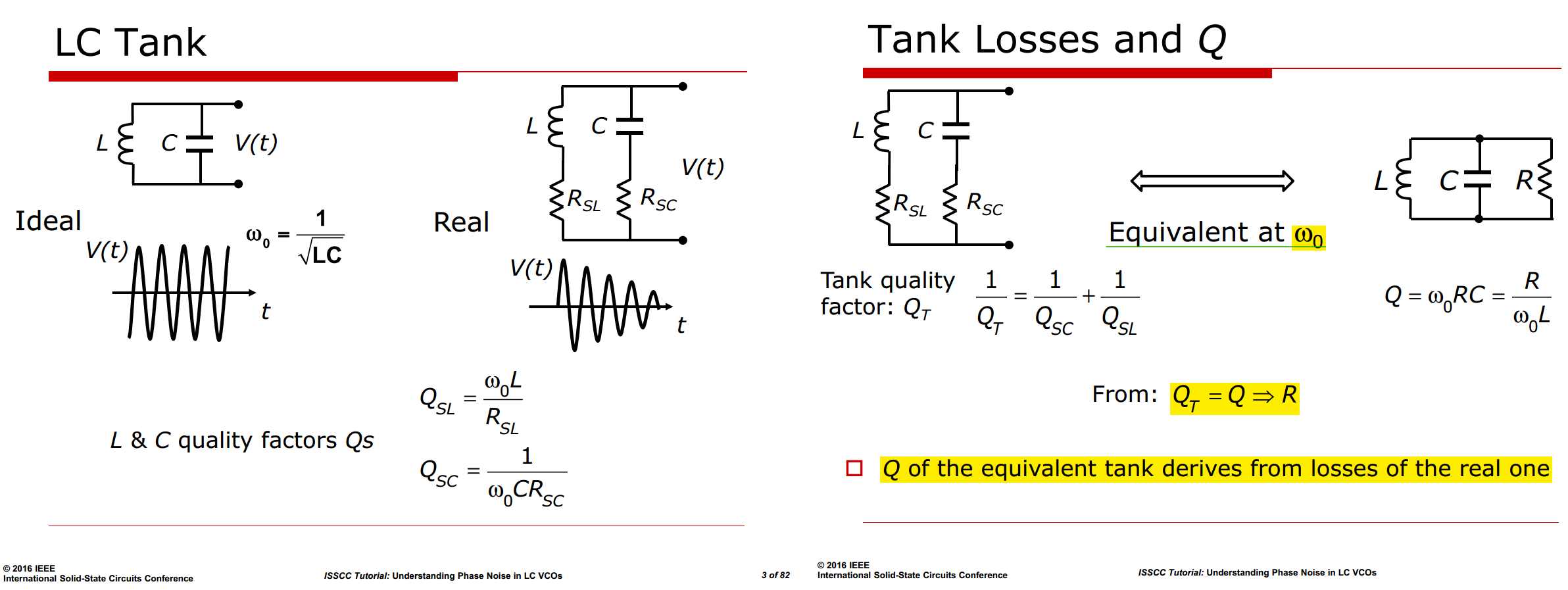
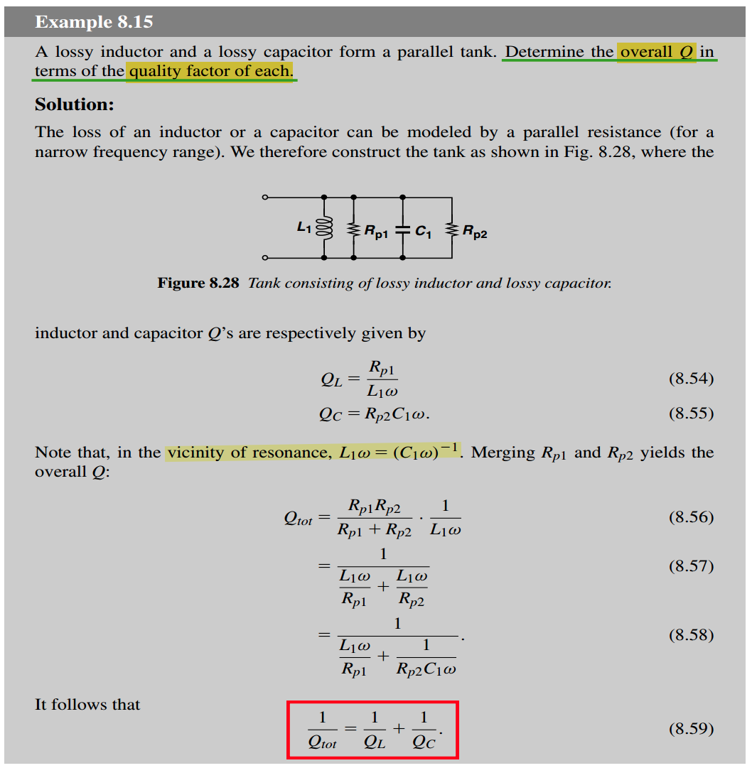
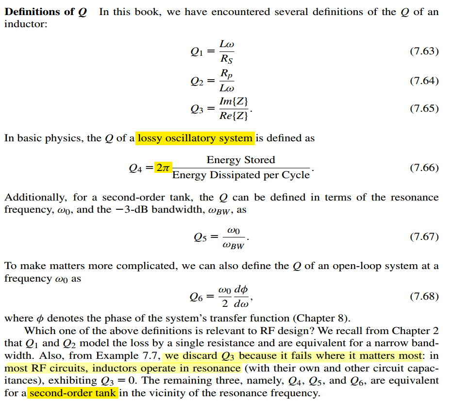
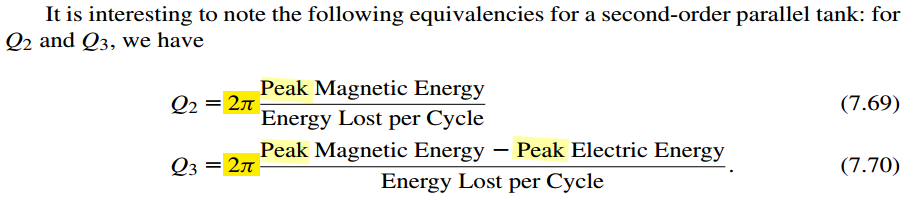
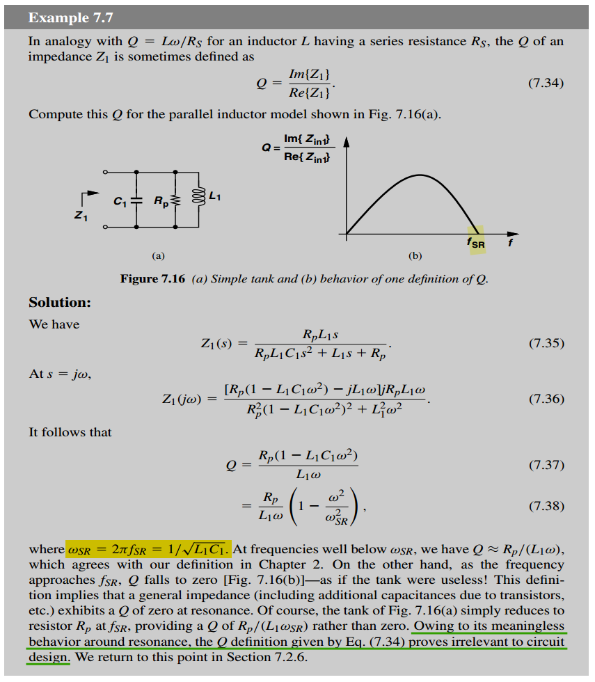
LC Tank Q
Definitions of Q
Assuming RLC oscillator waveform is \(V(t)=V_0\sin\omega_0 t\), \(\omega_0 = \frac{1}{\sqrt{LC}}\) is
resonant frequency
Energy stored \[
E_t = \frac{1}{2}LI_0^2 = \frac{1}{2}CV_0^2
\] Energy Dissipated per Cycle \[
E_d = \frac{V_0^2}{2R}\frac{2\pi}{\omega_0}
\] For \(Q_4\), with \(I_0=C\omega_0V_0\)\[
\boxed{Q_4 = 2\pi\frac{E_s}{E_d} = R\omega_0C = \frac{R}{\omega_0L}}
\]
which holds at resonance
For \(Q_3\), suppose RLC tank is
driven by \(V_o\cos \omega t\) voltage
source, then
Peak Magnetic Energy\[
E_{pL} = \frac{1}{2}LI_0^2 =
\frac{1}{2}L\left(\frac{V_0}{L\omega}\right)^2
\]Peak Electric Energy\[
E_{pC} = \frac{1}{2}CV_0^2
\] with Energy Lost per Cycle\(E_d =
\frac{V_0^2}{2R}\frac{2\pi}{\omega_0}\), we have \[
Q_3 = \frac{E_{pL} - E_{pC}}{E_d} =
\left(\frac{1}{L\omega^2}-C\right)R\omega=\frac{R}{L\omega}\left(1 -
\frac{\omega^2}{\omega^2_{SR}}\right)
\]
A. L. S. Loke et al., "A versatile low-jitter PLL in 90-nm
CMOS for SerDes transmitter clocking," Proceedings of the IEEE 2005
Custom Integrated Circuits Conference, 2005., San Jose, CA, USA,
2005 [slides,
paper]
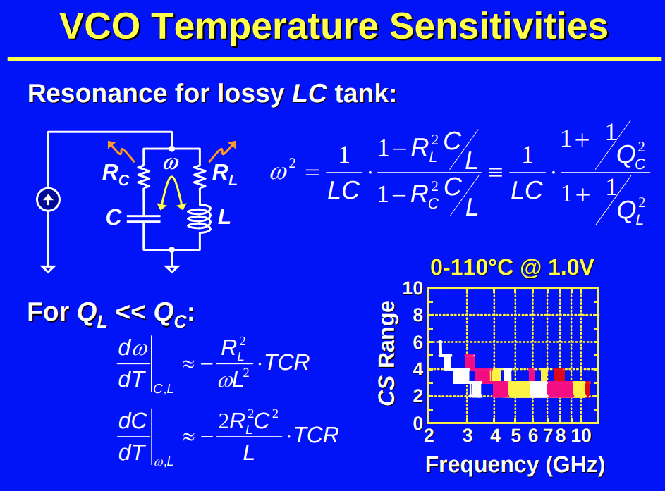
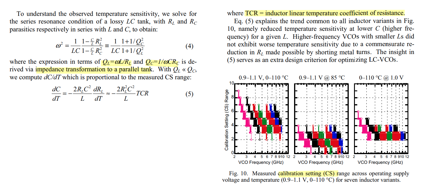
\[
f=\frac{1}{2\pi\sqrt{L_p C_p}} =
\frac{1}{2\pi\sqrt{L_s\frac{Q_L^2+1}{Q_L^2} C_s\frac{Q_C^2}{Q_C^2+1}}} =
\frac{1}{2\pi\sqrt{L_sC_s}}\cdot \sqrt{\frac{1+1/Q_c^2}{1+1/Q_L^2}}
\] Assuming the tank's Q is limited by the inductor's quality
factor \(Q_L\), i.e. \(Q_L\ll Q_c\)\[
f\approx \frac{1}{2\pi\sqrt{L_sC_s}}\cdot \sqrt{1-\frac{1}{Q_L^2}}
=f_0\cdot\sqrt{1-\frac{1}{Q_L^2}}
\] where \(f_0=\frac{1}{\sqrt{L_sC_s}}\) is the first
order approximation of the resonant frequency
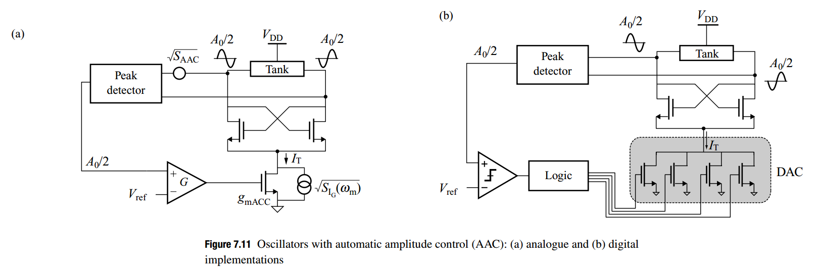
Automatic Amplitude Control
(AAC)
peak detector, envelope
detector
The digital AAC regulates the amplitude without increasing the
amplitude modulation noise
PN Reduction Techniques
Y. Hu, T. Siriburanon and R. B. Staszewski, "Oscillator Flicker Phase
Noise: A Tutorial," in IEEE Transactions on Circuits and Systems II:
Express Briefs, vol. 68, no. 2, pp. 538-544, Feb. 2021 [paper]
[slides]
with \(\boxed{x(t) = \cos(\omega_0
t)}\)\[
y_{\cos}(t) =
\underbrace{\frac{\alpha_2}{2}+\frac{3\alpha_4}{8}}_{\text{DC}}
+ \underbrace{\left(\alpha_1+\frac{3\alpha_3}{4}\right)\cos(\omega_0
t)}_{\omega_0}
+ \underbrace{\frac{\alpha_2+\alpha_4}{2}\cos(2\omega_0 t)}_{2\omega_0}
+ \underbrace{\frac{\alpha_3}{4}\cos(3\omega_0 t)}_{3\omega_0}
+ \underbrace{\frac{\alpha_4}{8}\cos(4\omega_0 t)}_{4\omega_0}
\] They're the same waveform; one is the other shifted in time by
a quarter of the fundamental period: \[
y_{\cos}(t) = y_{\sin}\!\left(t + \frac{T}{4}\right), \qquad T =
\frac{2\pi}{\omega_0}
\]
given \(\Delta t\) is constant \[
\boxed{\Delta t = \frac{\Delta\Phi_N}{N\omega_0} \implies \Delta\Phi_N =
N\Delta\Phi_0 \quad (\Delta t = \text{constant})}
\]
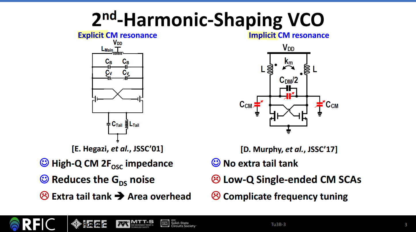
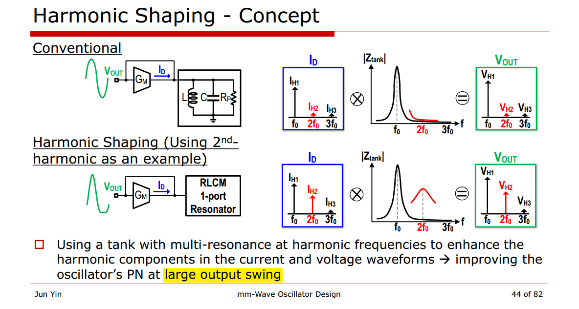
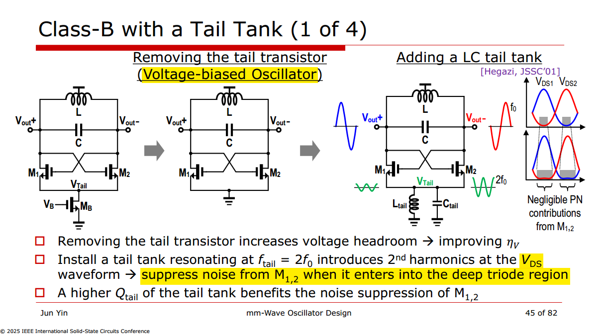
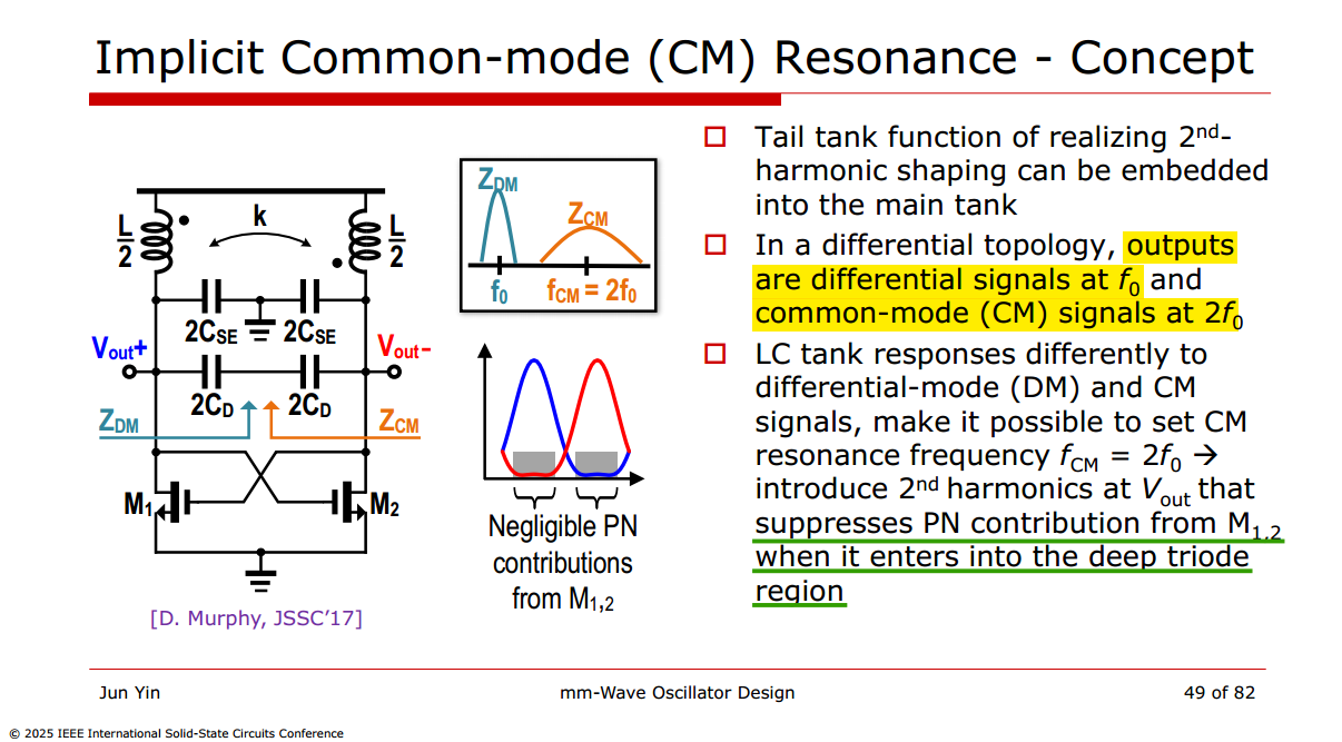
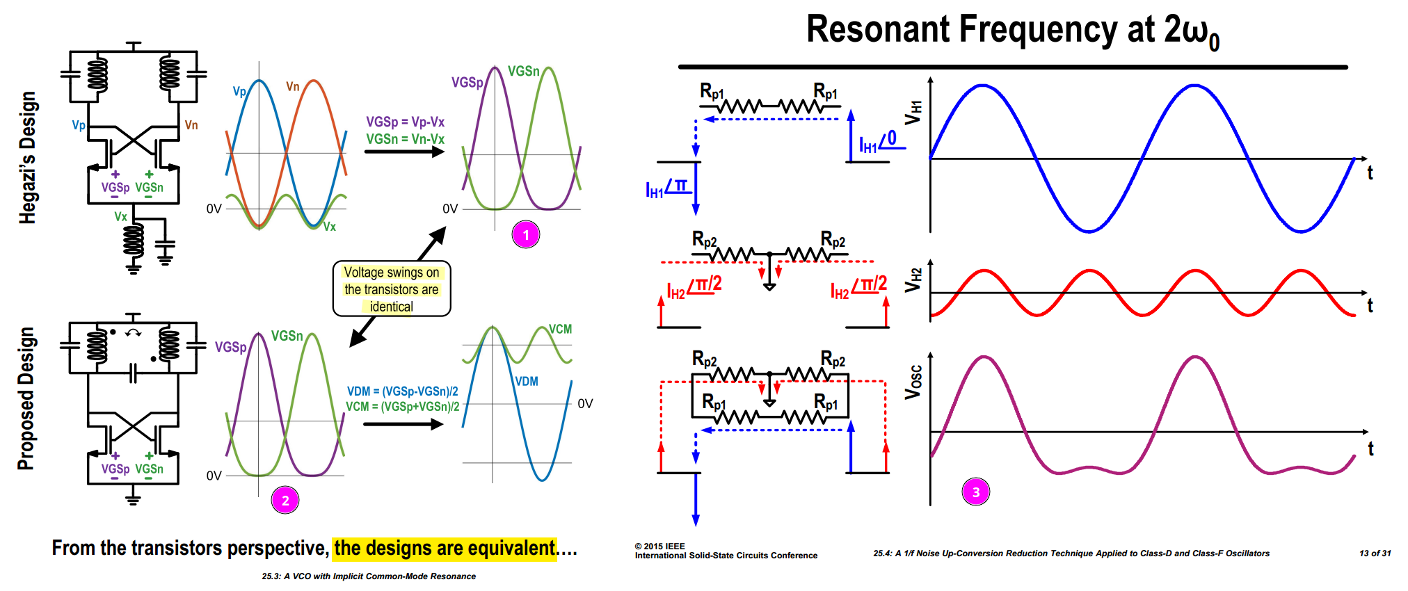
Harmonic Shaping
E. Hegazi, H. Sjoland and A. Abidi, "A filtering technique to lower
oscillator phase noise," 2001 IEEE International Solid-State
Circuits Conference. Digest of Technical Papers. ISSCC (Cat.
No.01CH37177), San Francisco, CA, USA, 2001 [paper,
slides]
A. Bevilacqua and P. Andreani, "An Analysis of 1/f Noise to Phase
Noise Conversion in CMOS Harmonic Oscillators," in IEEE Transactions on
Circuits and Systems I: Regular Papers, vol. 59, no. 5, pp. 938-945, May
2012
D. Murphy, H. Darabi and H. Wu, "Implicit Common-Mode Resonance in LC
Oscillators," in IEEE Journal of Solid-State Circuits, vol. 52, no. 3,
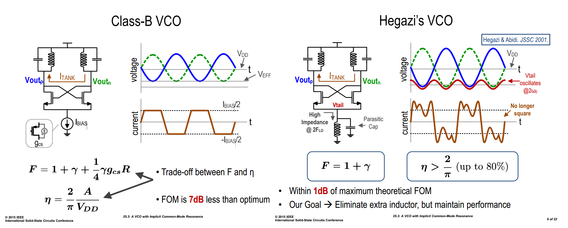
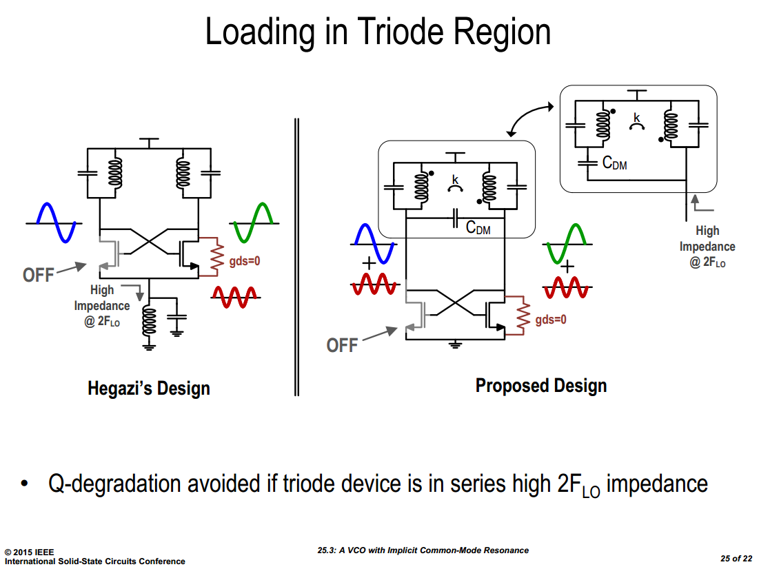
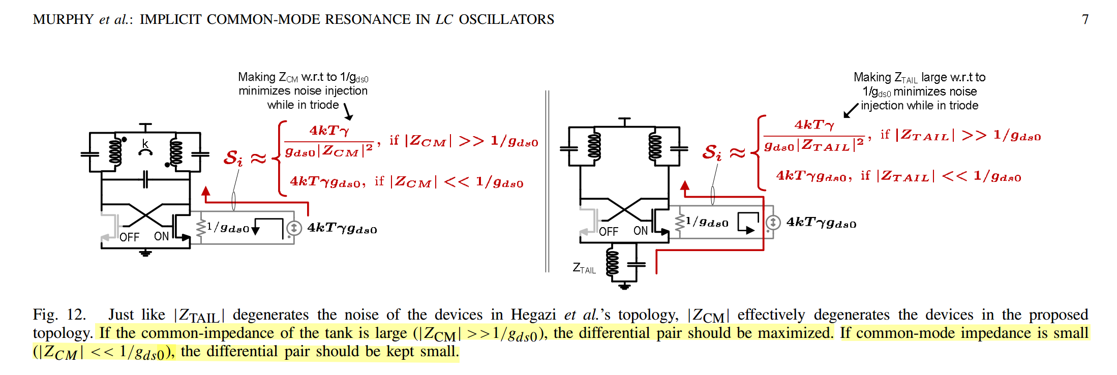
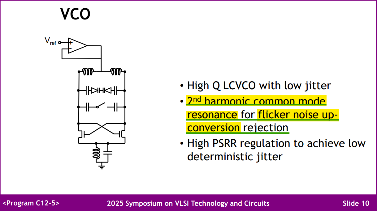
pp. 812-821, March 2017, [https://sci-hub.st/10.1109/JSSC.2016.2642207]
—, "25.3 A VCO with implicit common-mode resonance," 2015 IEEE
International Solid-State Circuits Conference - (ISSCC) Digest of
Technical Papers, San Francisco, CA, USA, 2015 [https://sci-hub.st/10.1109/ISSCC.2015.7063116]
M. Shahmohammadi, M. Babaie and R. B. Staszewski, "25.4 A 1/f noise
upconversion reduction technique applied to Class-D and Class-F
oscillators," 2015 IEEE International Solid-State Circuits Conference -
(ISSCC) Digest of Technical Papers, San Francisco, CA, USA, 2015 [https://sci-hub.ru/10.1109/ISSCC.2015.7063117]
Michael Perrott August 12, 2008, Short Course On Phase-Locked Loops
and Their Applications Day 2, AM Lecture Basic Building Blocks
Voltage-Controlled Oscillators [https://www.cppsim.com/PLL_Lectures/day2_am.pdf]
Yunbo Huang, Zunsong Yang, et al., "A 7.0-to-8.6GHz Balanced
Class-F-1 VCO with a Trifilar Transformer-Based Tank Achieving
194.5dBc/Hz FoM," IEEE MTT-S Radio Frequency Integrated Circuits
(RFIC), June 2026
S. Gallucci et al., "A Low-Noise Digital PLL With an
Adaptive Common-Mode Resonance Tuning Technique for Voltage-Biased
Oscillators," in IEEE Journal of Solid-State Circuits, vol. 60,
no. 12, pp. 4572-4586, Dec. 2025 P. Liu et al., "A 128Gb/s ADC/DAC Based
PAM-4 Transceiver with >45dB Reach in 3nm FinFET," 2025 Symposium on
VLSI Technology and Circuits (VLSI Technology and Circuits), Kyoto,
Japan, 2025
Narrowing of conduction
angle
Y. Hu, T. Siriburanon and R. B. Staszewski, "Intuitive Understanding
of Flicker Noise Reduction via Narrowing of Conduction Angle in
Voltage-Biased Oscillators," in IEEE Transactions on Circuits and
Systems II: Express Briefs, vol. 66, no. 12, pp. 1962-1966, Dec. 2019
[https://sci-hub.se/10.1109/TCSII.2019.2896483]
TODO 📅
Gate-drain phase shift
TODO 📅
simulation in oscillator
varactor simulation
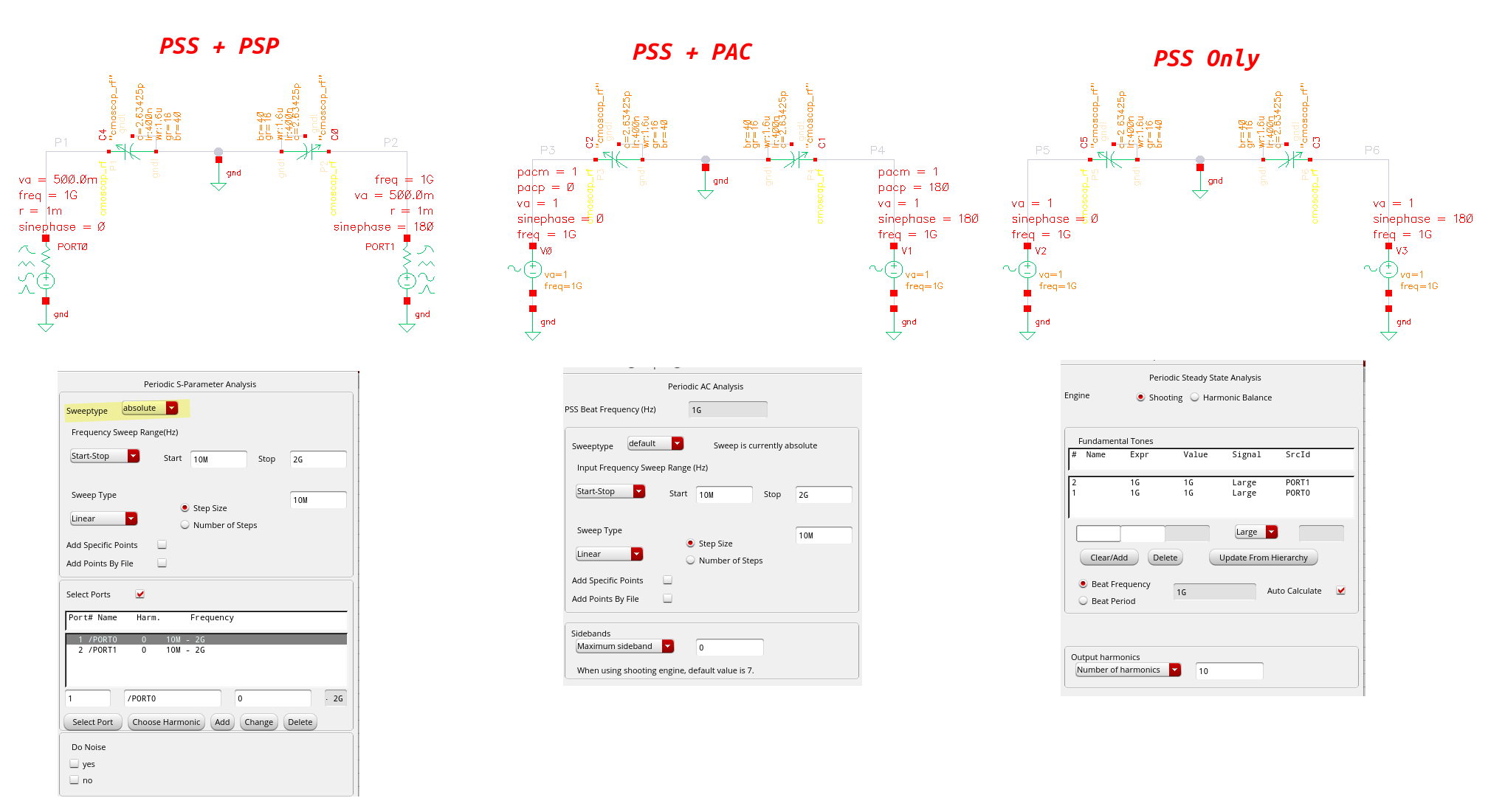
Three methods:
PSS +PSP (pay attention to port termination and voltage
amplitude)
PSS +PAC
PSS Only
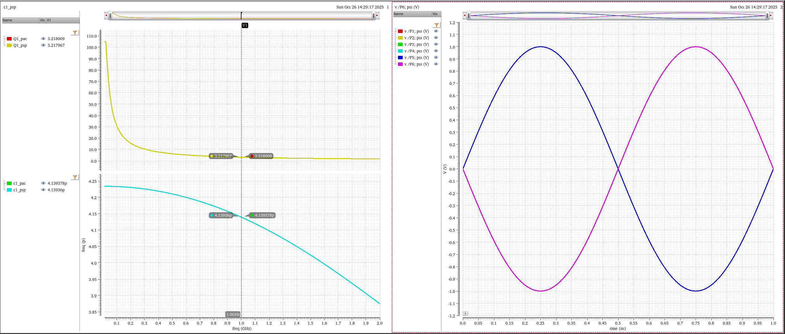
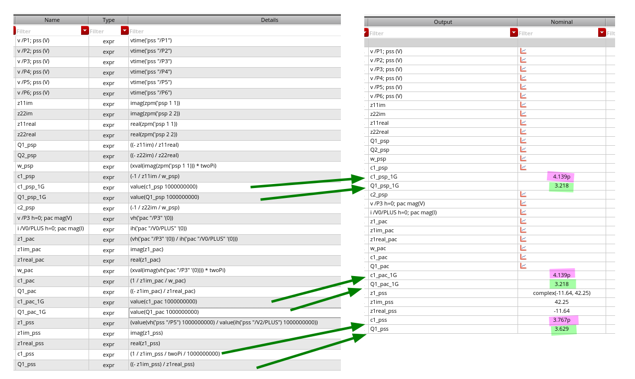
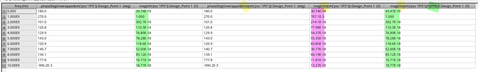
rms only scale magnitude \(1/\sqrt{2}\) but retain phase for complex
number, like harmonic
C. Samori, "Tutorial: Understanding Phase Noise in LC VCOs," 2016
IEEE International Solid-State Circuits Conference (ISSCC), San
Francisco, CA, USA, 2016
—, "Understanding Phase Noise in LC VCOs: A Key Problem in RF
Integrated Circuits," in IEEE Solid-State Circuits Magazine,
vol. 8, no. 4, pp. 81-91, Fall 2016 [https://sci-hub.se/10.1109/MSSC.2016.2573979]
Jun Yin. ISSCC 2025 T10: mm-Wave Oscillator Design
Peter Kinget, ISSCC 2010 short course, Transistor-Level Design of
Critical PLL Circuits
J. Bank, "A harmonic-oscillator design methodology based on
describing functions," Ph.D. dissertation, Dept. Signals Syst., Sch.
Elect. Eng., Chalmers Univ. Techn., Chalmers, Sweden, 2006. [https://publications.lib.chalmers.se/records/fulltext/17376.pdf]
—. Design of CMOS Phase-Locked Loops: From Circuit Level to
Architecture Level. Cambridge University Press; 2020.
Lacaita, Andrea Leonardo, Salvatore Levantino, and Carlo Samori.
Integrated frequency synthesizers for wireless systems.
Cambridge University Press, 2007
K. -H. Cheng, C. -L. Hung, C. -H. Chang, Y. -L. Lo, W. -B. Yang and
J. -W. Miaw, "A Spread-Spectrum Clock Generator Using Fractional-N PLL
Controlled Delta-Sigma Modulator for Serial-ATA III," 2008 11th IEEE
Workshop on Design and Diagnostics of Electronic Circuits and
Systems, Bratislava, Slovakia, 2008 [https://sci-hub.se/10.1109/DDECS.2008.4538758]
Due to \(f= K_{vco}V_{ctrl}\), its
derivate to \(t\) is \[
\frac{\mathrm{d}f}{\mathrm{d}t} =
K_{vco}\frac{\mathrm{d}V_{ctrl}}{\mathrm{d}t}
\]
For chargepump PLL, \(dV_{ctrl} =
\frac{\phi_e I_{cp}}{2\pi C}dt\), that is \[
\frac{\mathrm{d}f}{\mathrm{d}t} = K_{vco} \frac{\phi_e I_{cp}}{2\pi C}
\]
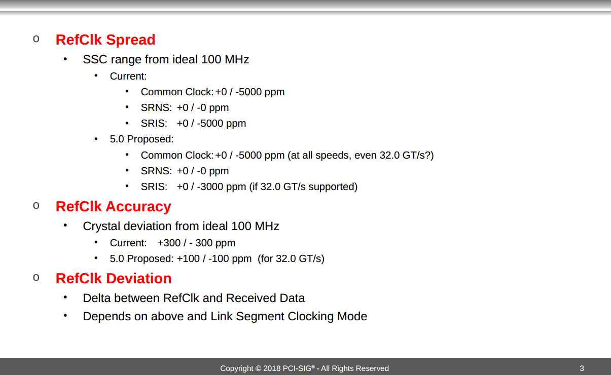
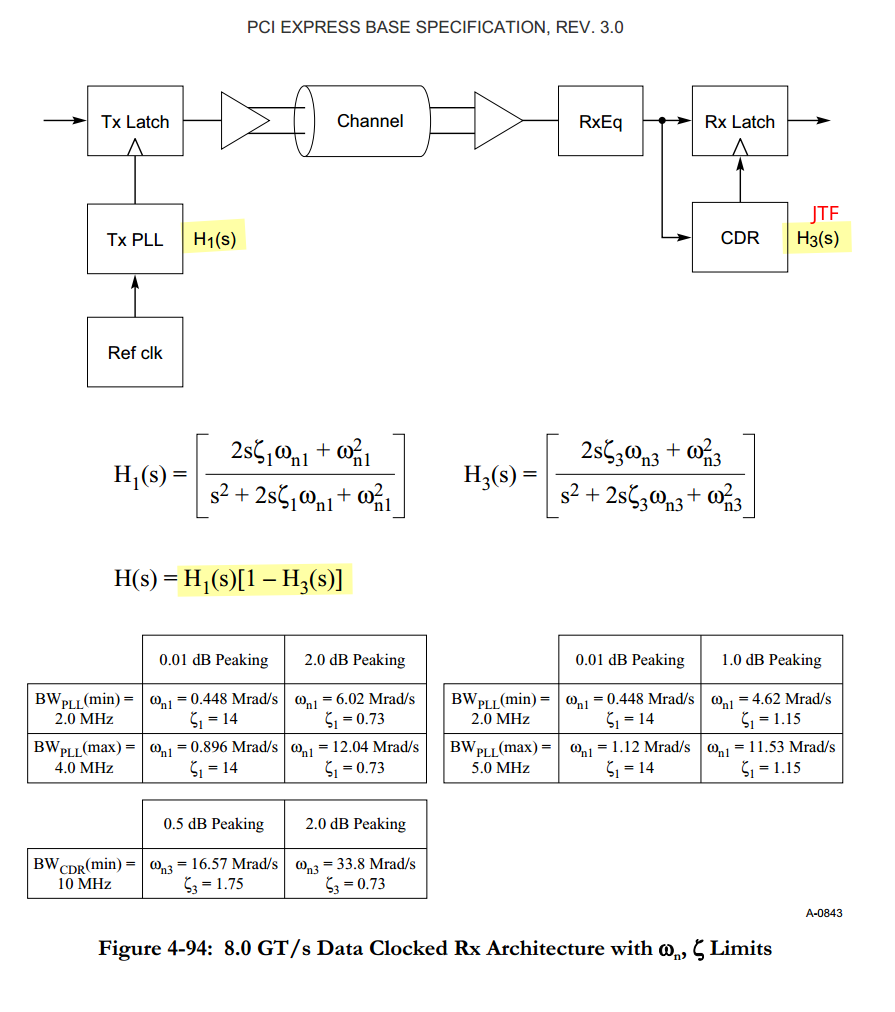
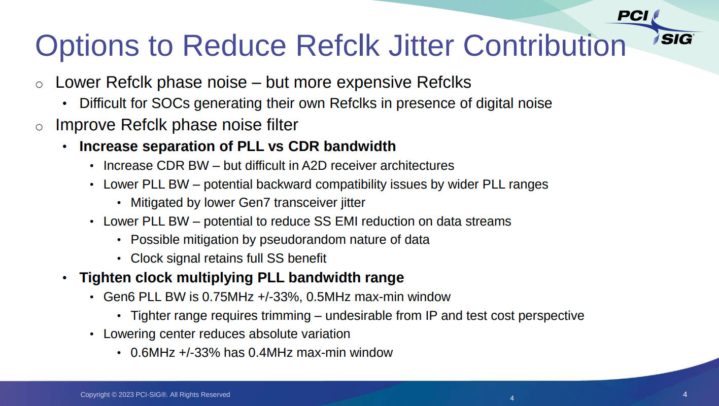
Refclk Clocking
Architectures
PCI Express Base Specification Revision 3.0
Jeff Morriss, Intel Gerry Talbot, AMD. PCI-SIG Devcon 2006. Jitter
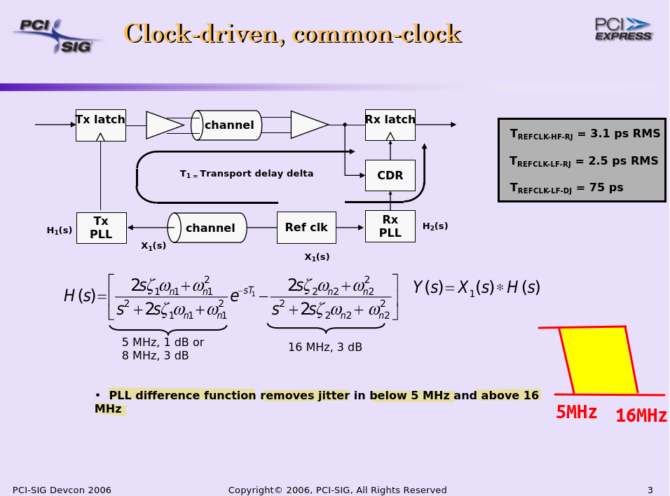
Budgeting for Clock Architecture
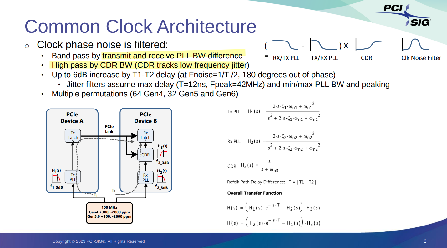
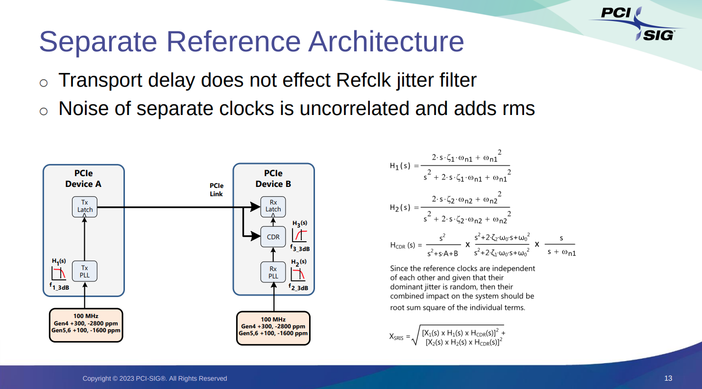
Common Refclk Rx architectures are characterized by the Tx and Rx
sharing the same Refclk source
Most of the SSC jitter sourced by the Refclk is propagated equally
through Tx and Rx PLLs, and so intrinsically tracks LF
jitter
The amount of jitter appearing at the CDR is then defined by the
difference function between the Tx and Rx PLLs multiplied by the
CDR highpass characteristic
\[
H(s)= H_1(s)e^{-sT} - \left[H_1(s)e^{-sT}(1-H_3(s)) + H_2(s)H_3(s)
\right] = [H_1(s)e^{-sT} -H_2(s)]H_3(s)
\] where \(H_3(s)\) is similar
to \(NTF_{VCO}\), \(1-H_3(s)\) is similar to \(NTF_{REF}\)
Data Clocked Refclk Rx
Architecture
A data clocked Rx architecture is characterized by requiring the
receiver's CDR to track the entirety of the low frequency jitter,
including SSC
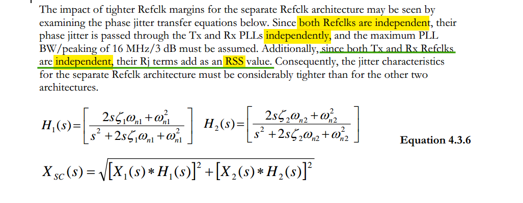
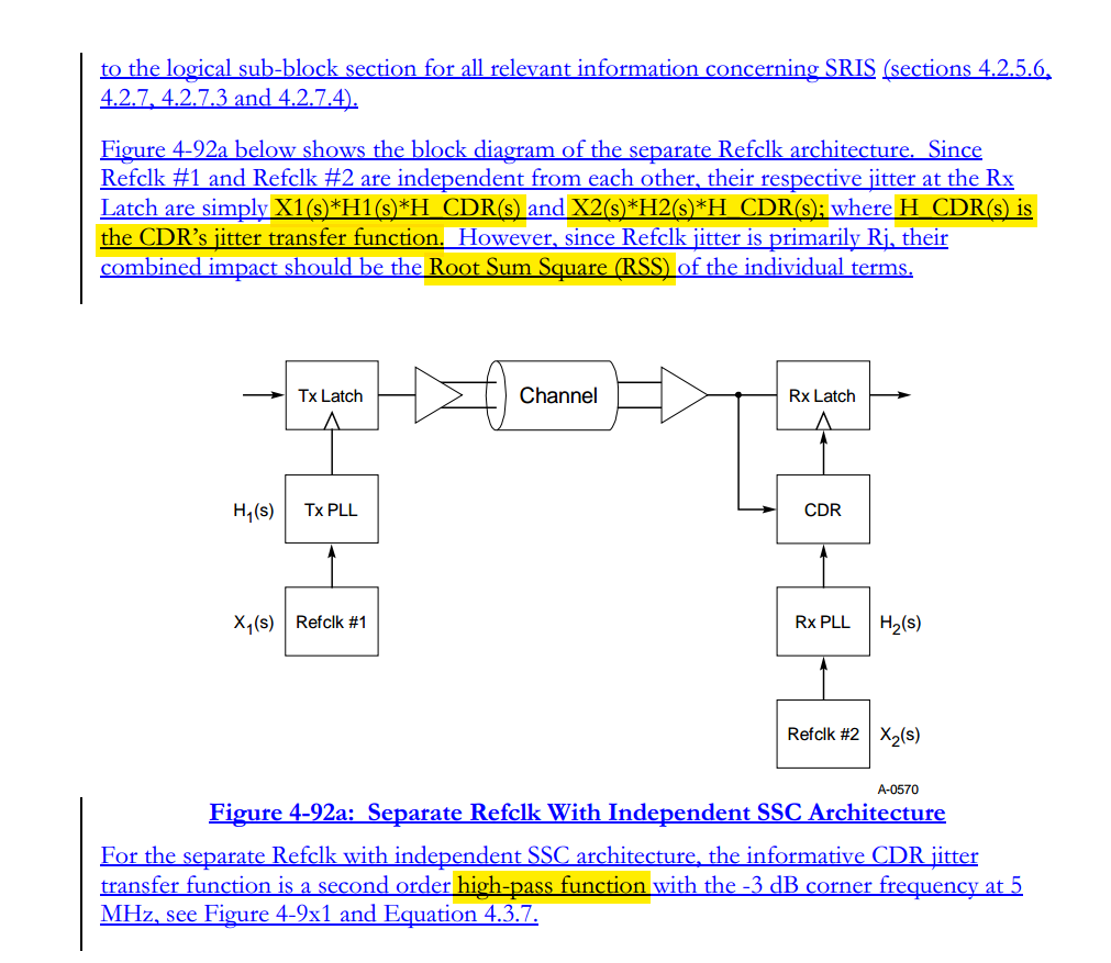
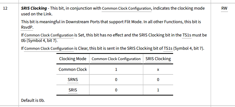
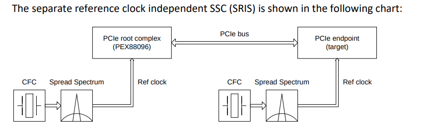
Separate Reference
Clocks with SSC (SRIS)
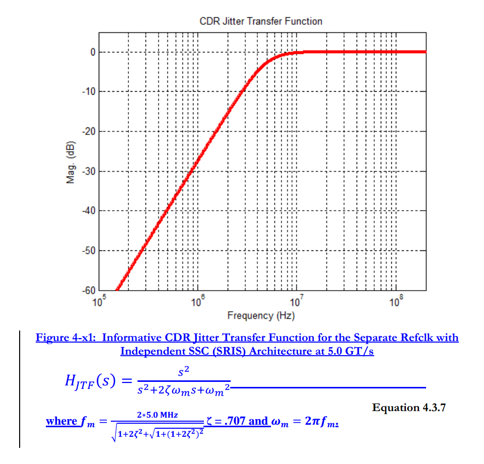
TITLE: Separate Refclk Independent SSC Architecture (SRIS) DATE:
Updated 10 January 2013 AFFECTED DOCUMENT: PCI Express Base Spec. Rev.
3.0 SPONSOR: Intel, HP, AMD
\[\begin{align}
X_{LATCH}(s) &= X_1(s)H_1(s) - \left[X_1(s)H_1(s)(1-H_3(s)) +
X_2(s)H_2(s)H_3(s) \right] \\
& = \left[X_1(s)H_1(s) -X_2(s)H_2(s)\right]H_3(s)
\end{align}\] where \(H_3(s)\)
is similar to \(NTF_{VCO}\), \(1-H_3(s)\) is similar to \(NTF_{REF}\)
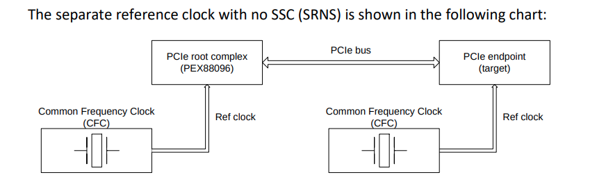
Separate Reference
Clocks with No SSC (SRNS)
Refclk Jitter Filter
Analysis
Greg Richmond Skyworks, Inc. July 27, 2023, 128GTps (Gen7) Refclk
Jitter Filter Analysis
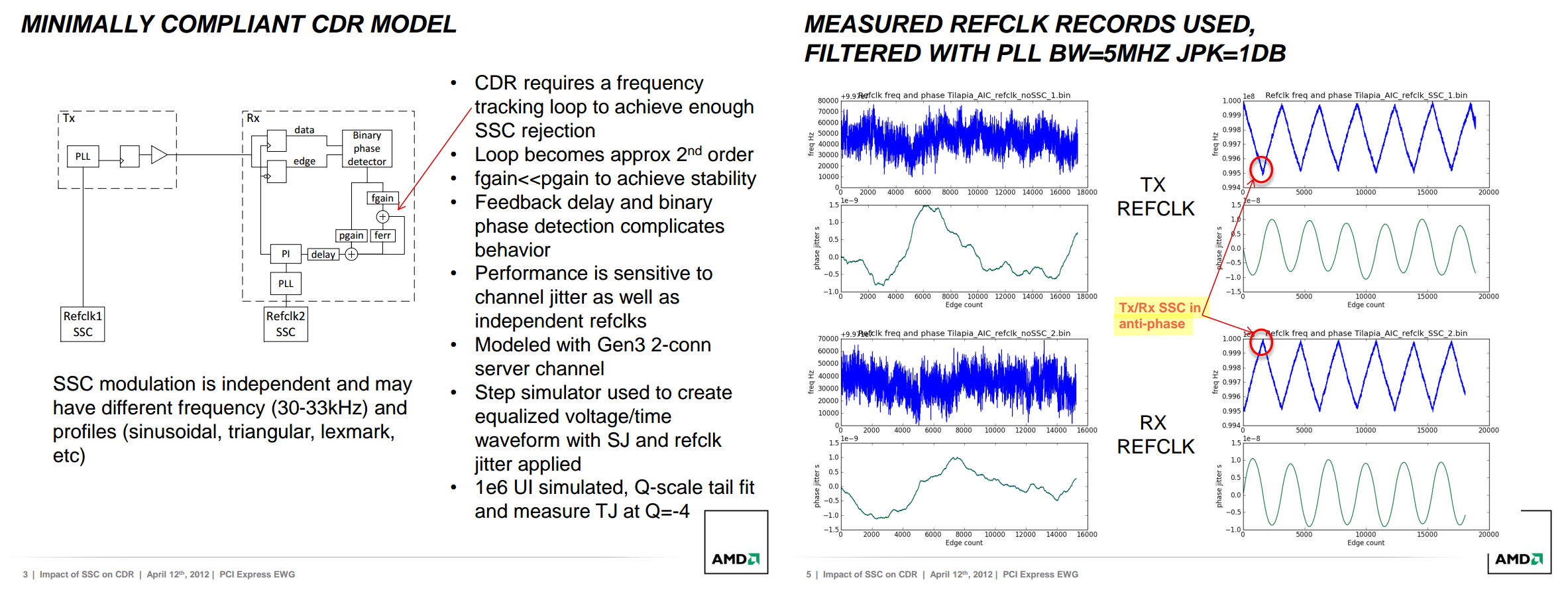
SSC on digital CDR
Gerry Talbot, "Impact of SSC on CDR" , April 12th, 2012, PCI Express
EWG
K. -H. Cheng, C. -L. Hung, C. -H. Chang, Y. -L. Lo, W. -B. Yang and
J. -W. Miaw, "A Spread-Spectrum Clock Generator Using Fractional-N PLL
Controlled Delta-Sigma Modulator for Serial-ATA III," 2008 11th IEEE
Workshop on Design and Diagnostics of Electronic Circuits and
Systems, Bratislava, Slovakia, 2008 [https://sci-hub.se/10.1109/DDECS.2008.4538758]
Rhee, W. (2020). Phase-locked frequency generation and clocking :
architectures and circuits for modern wireless and wireline
systems. The Institution of Engineering and Technology
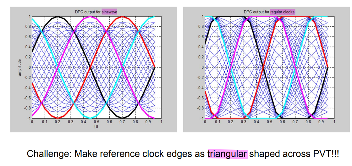
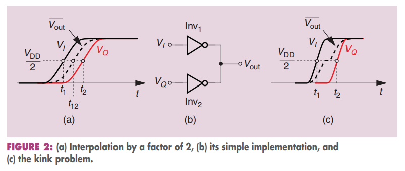
the interpolating inverters near the midscale can be made weaker so
as to obtain more uniform phase increments. Alternatively, those at the
top and bottom of the array can be made stronger
Single-Quadrant PI
\[
V_o(t) = m \cdot \sin(\omega t + \frac{\pi}{2}) + p\cdot \sin(\omega t)
= m\cdot \cos(\omega t) + p\cdot \sin(\omega t) = \sqrt{m^2+p^2}
\sin(\omega t + \phi)
\]
where \(\tan \phi = \frac{m}{p} =
\frac{1-p}{p}\) and \(p =
\frac{1}{1+\tan \phi}\)
A constant Output amplitude is desired because the
swing-dependent delay characteristic of the CML-to-CMOS (C2C)
circuit results in AM–PM distortion which eventually manifests
as phase nonlinearity
Current-Mode Phase
Interpolator
Voltage-Mode Phase
Interpolator
Integrating-Mode Phase
Interpolator
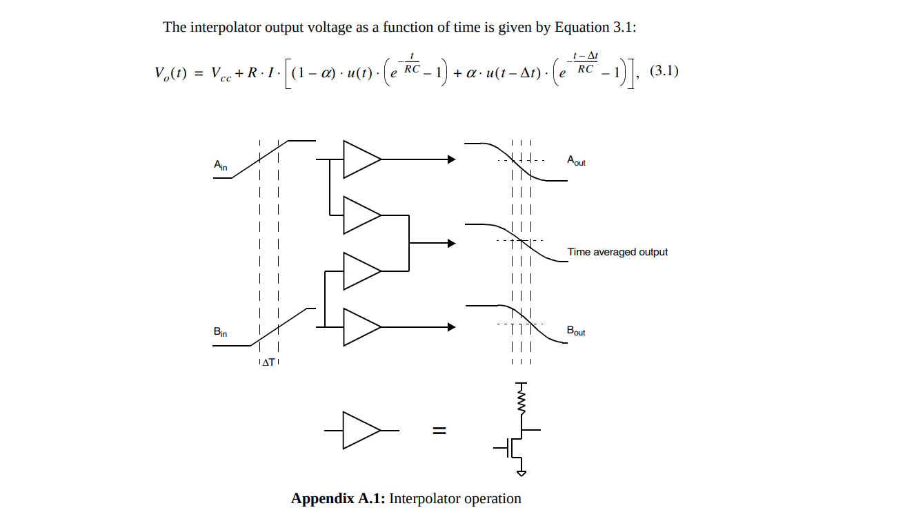
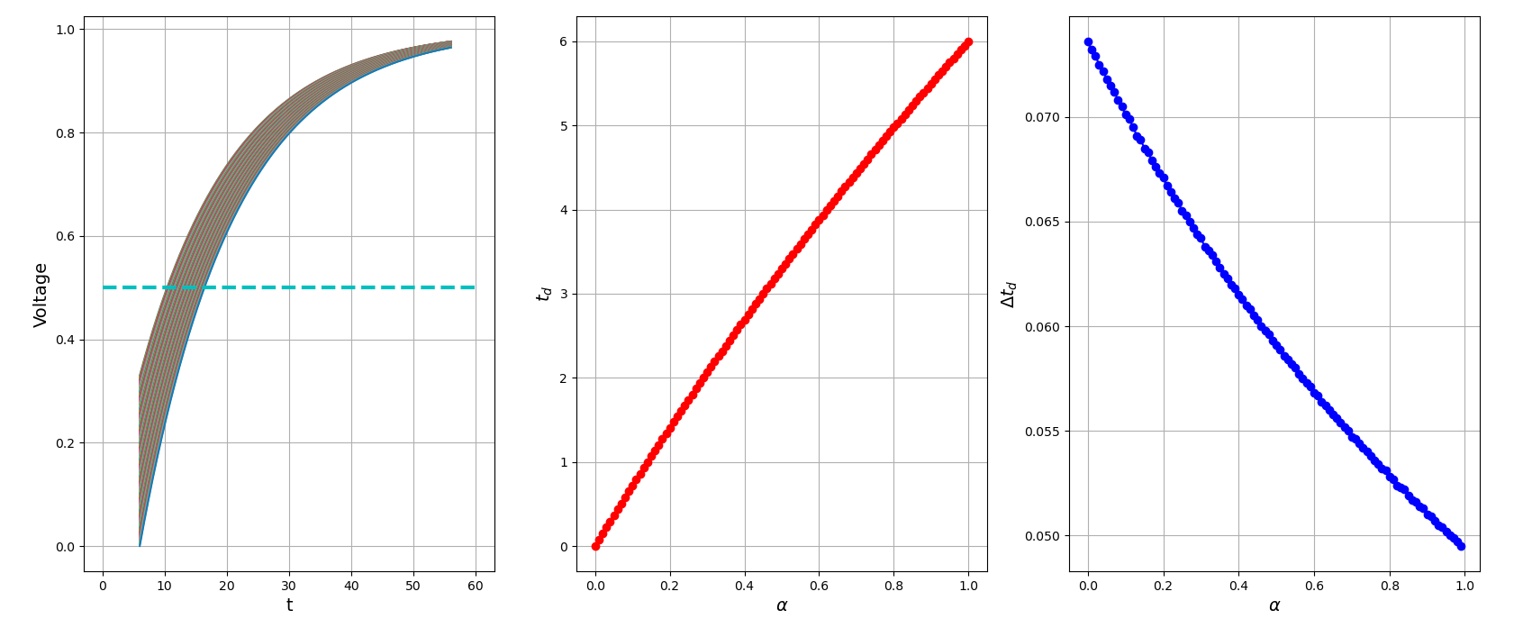
PI vs. PLL based CDR
PCI Express Jitter Modeling Revision 1.0RD July 14, 2004
A. K. Mishra, Y. Li, P. Agarwal and S. Shekhar, "Improving Linearity
in CMOS Phase Interpolators," in IEEE Journal of Solid-State Circuits,
vol. 58, no. 6, pp. 1623-1635, June 2023 [pdf]
Cortiula A, Menin D, Bandiziol A, Driussi F, Palestri P. Modeling of
Phase-Interpolator-Based Clock and Data Recovery for High-Speed PAM-4
Serial Interfaces. Electronics. 2025; [https://www.mdpi.com/2079-9292/14/10/1979]
G. Souliotis, A. Tsimpos and S. Vlassis, "Phase Interpolator-Based
Clock and Data Recovery With Jitter Optimization," in IEEE Open
Journal of Circuits and Systems, vol. 4, pp. 203-217, 2023 [https://ieeexplore.ieee.org/document/10184121]
Beer, Salomon & Priel, Michael & Dobkin, Rostislav &
Kolodny, Avinoam. (2010). The Devolution of Synchronizers. Proceedings -
International Symposium on Asynchronous Circuits and Systems. [pdf]
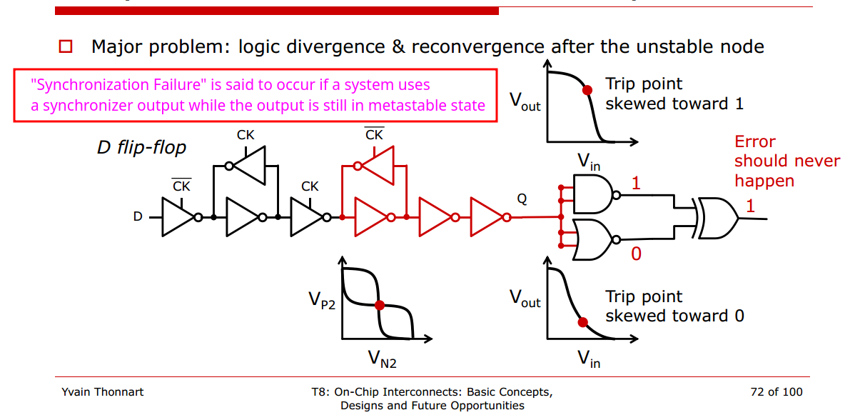
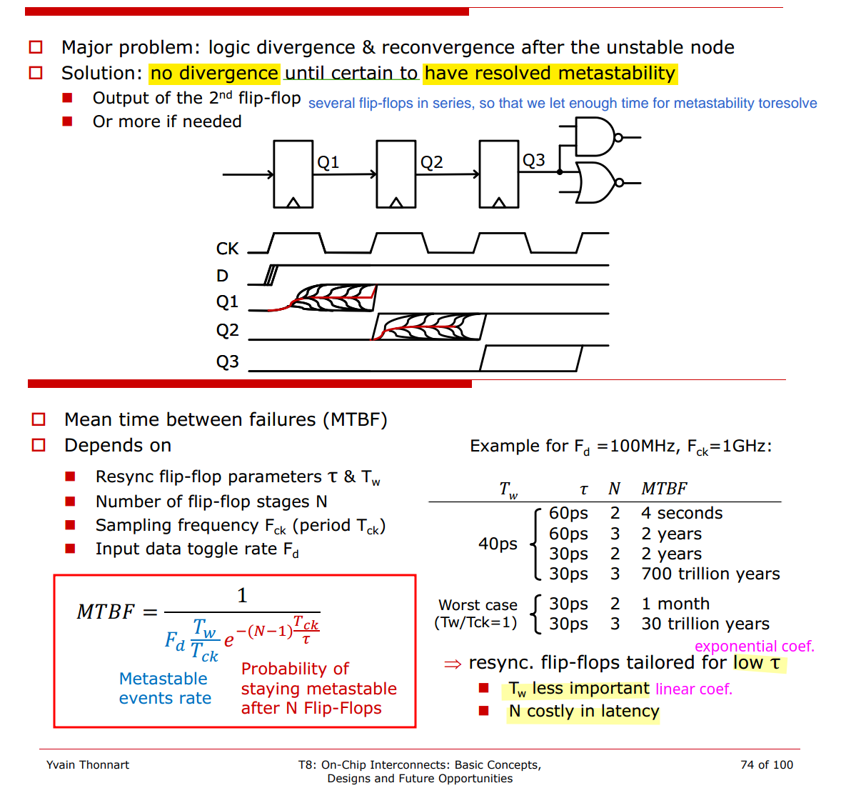
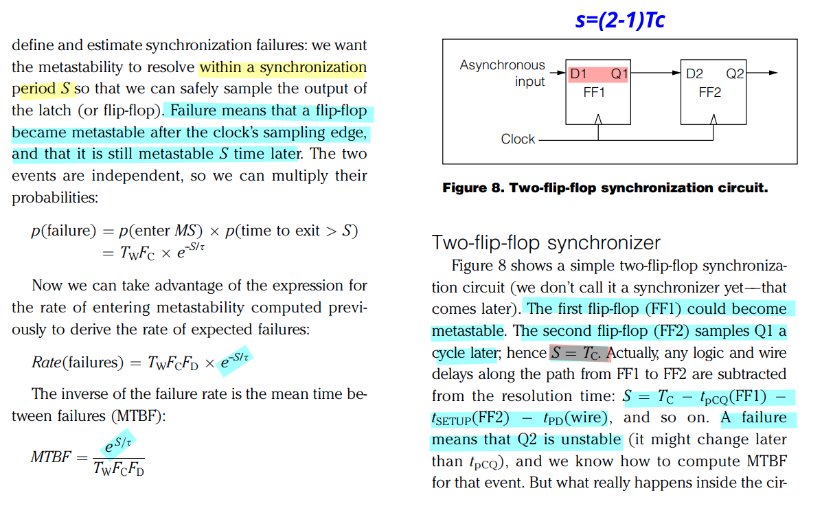
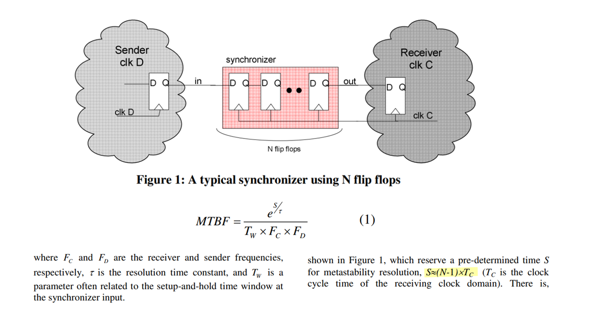
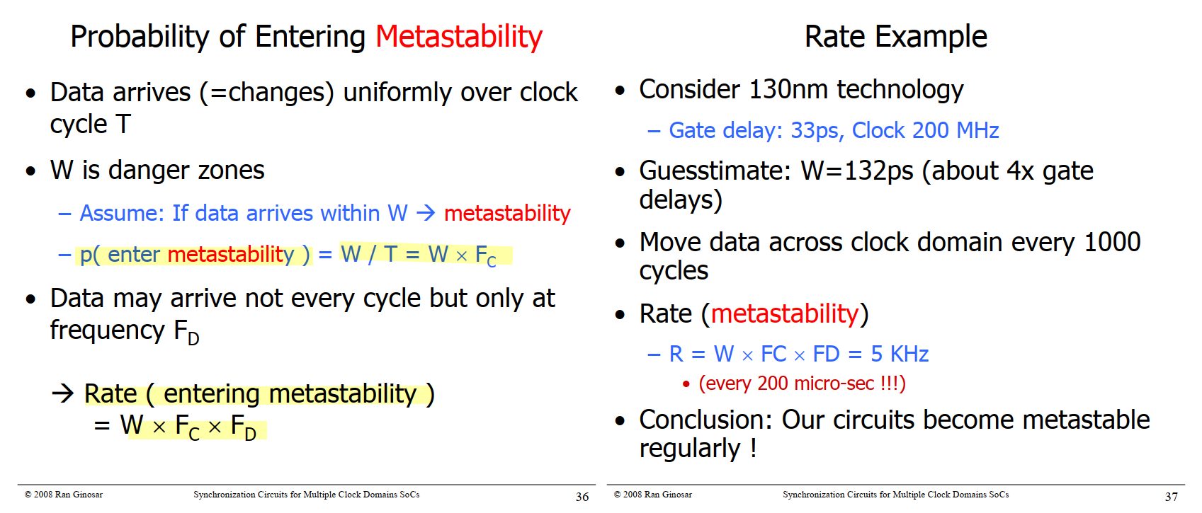
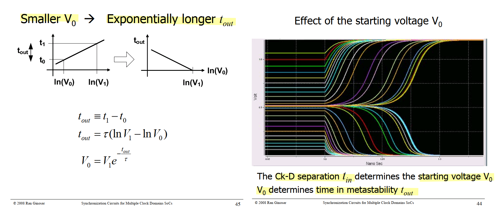
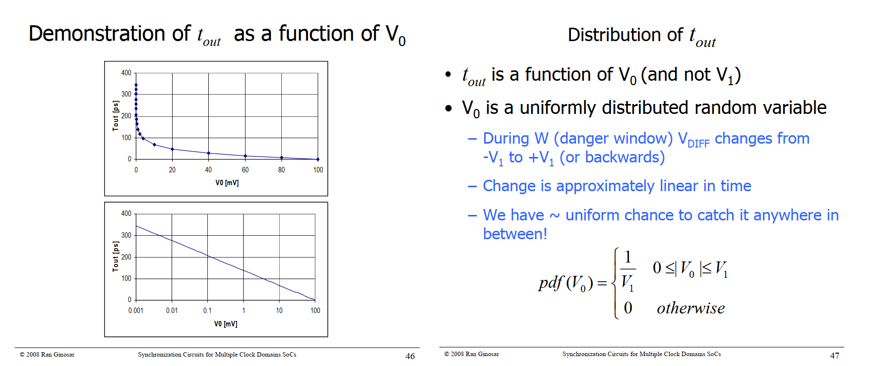
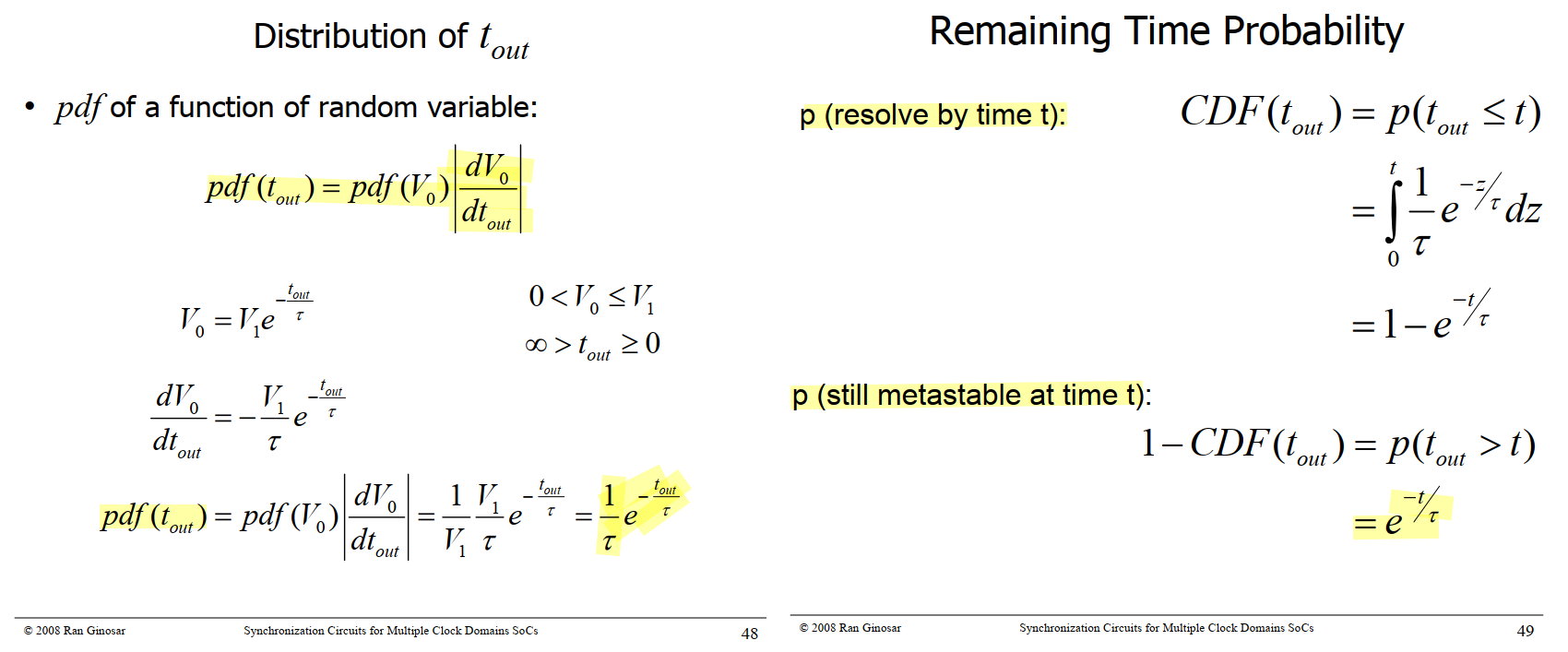
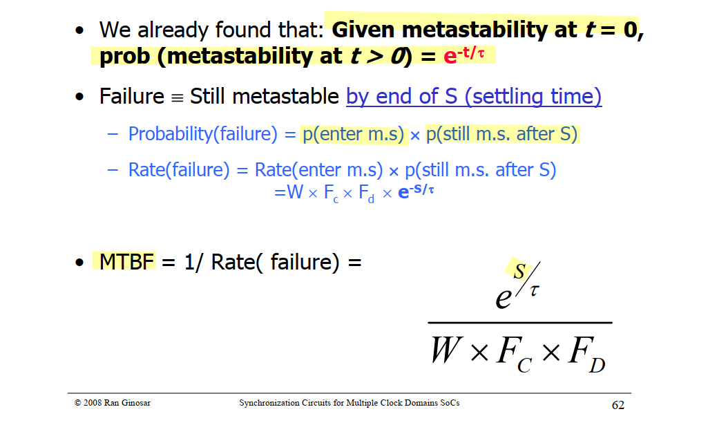
\(T_W\), metastability window is
defined differently among published paper
Some PDK provide \(T_0\) and \(\tau\) for the corresponding cascaded flip
flop synchronizer stdcells \[
\text{MTBF} = \frac{1}{T_W\times f_C\times f_D}\space \space
\text{,where}\space\space T_W = T_0 e^{-T_r/\tau}
\] and \(T_r = T_C - T_{DLY} -
T_{SU}\)
Ran Ginosar
ISCAS 2008 tutorial: Synchronization Circuits for Multiple Clock
Domains SoCs
Enter metastabilty
Exit metastabilty
MTBF (Mean Time Between Failures)
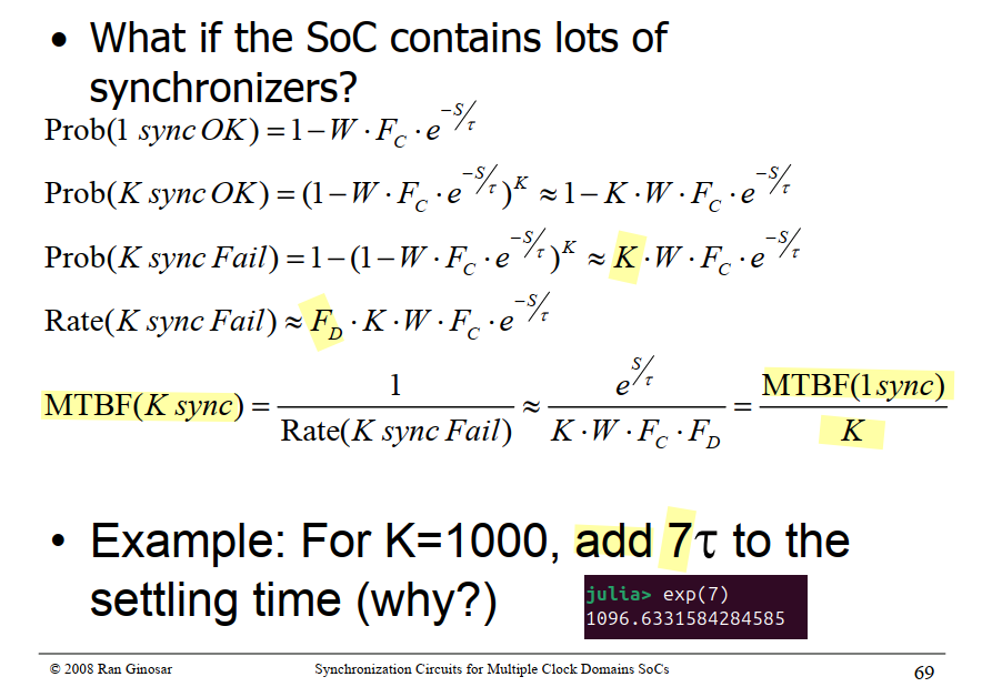
MTBF of Many Synchronizers
Synchronizer
Characterization
I. W. Jones, S. Yang and M. Greenstreet, "Synchronizer Behavior and
Analysis," 2009 15th IEEE Symposium on Asynchronous Circuits and
Systems, Chapel Hill, NC, USA, 2009 [https://sci-hub.ru/10.1109/ASYNC.2009.8]
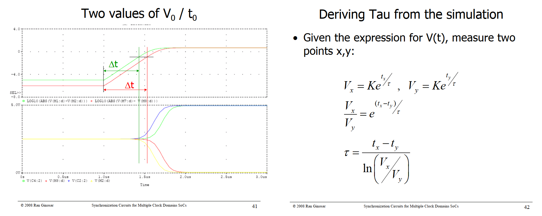
Xprova. bisect-tau - EDA tool for characterizing the metastability
resolution time constant (Tau) of bistable circuits [https://github.com/xprova/bisect-tau]
For GNU Octave, version 8.4.0, ngspice-42 : Circuit
level simulation program@Ubuntu 24.04.3 LTS x86_64
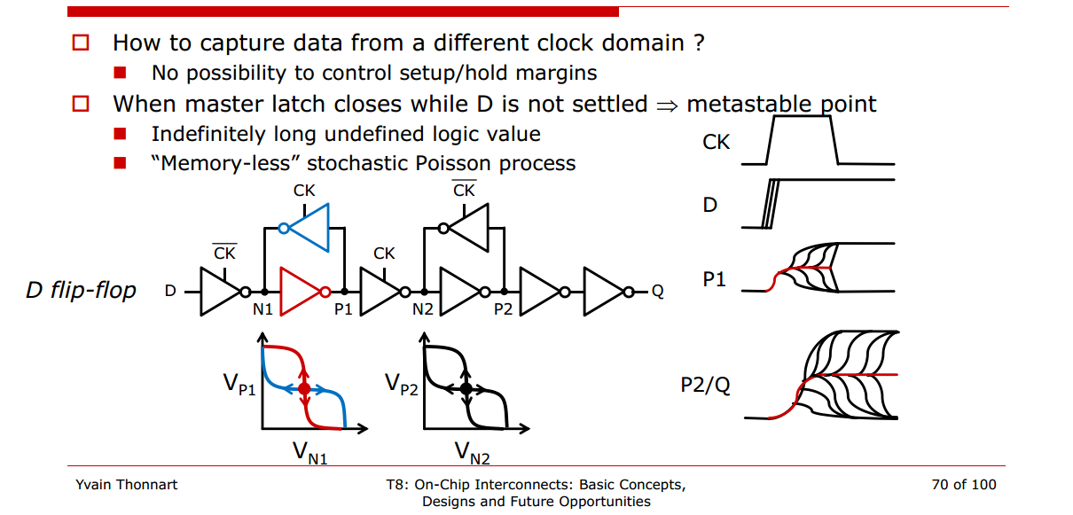
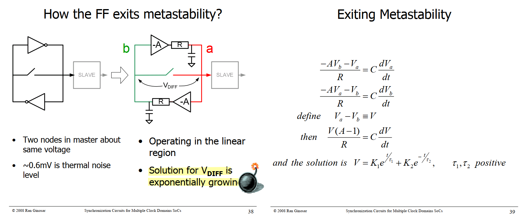
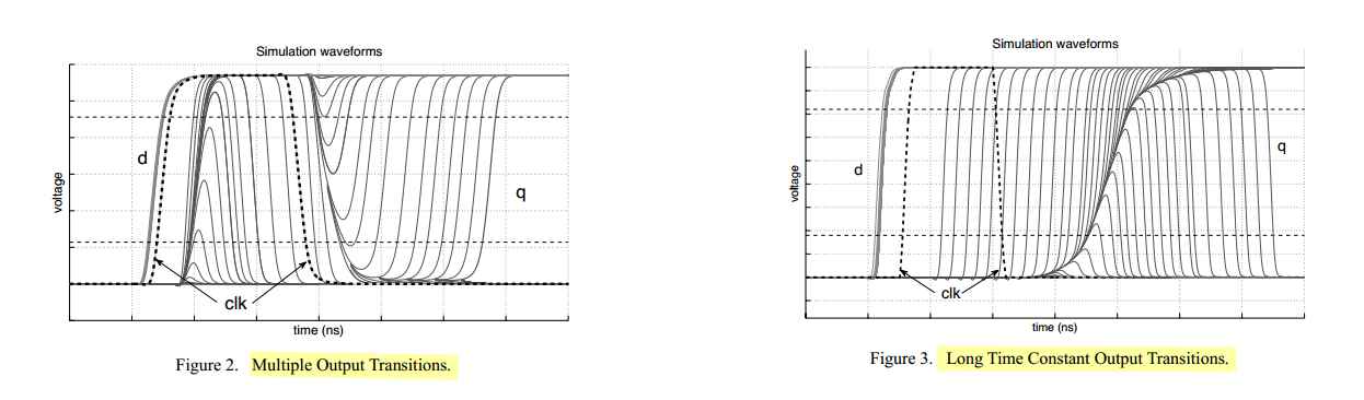
The typical flip-flops comprise master and slave latches and
decoupling inverters.
In metastability, the voltage levels of nodes A and B of the
master latch are roughly midway between logic 1 (VDD) and 0
(GND)
master latch enter metastability
In fact, one popular definition says that if the output of a
flip-flop changes later than the nominal clock-to-Q propagation
delay, then the flip-flop must have been metastable
Noise Seed—Seed for the random number generator (used by
the simulator to vary the noise sources internally). Specifying the
same seed allows you to reproduce a previous
experiment. The default value is 1.
Kinniment, D. J. Synchronization and arbitration in digital systems.
John Wiley & Sons Ltd (2007).
Synchronizers And Data FlipFlops are Different [pdf]
S. Beer, R. Ginosar, M. Priel, R. Dobkin and A. Kolodny, "The
Devolution of Synchronizers," 2010 IEEE Symposium on Asynchronous
Circuits and Systems, Grenoble, France, 2010 [pdf]
A dynamical system can be linear or nonlinear. Independently, it can
be deterministic or stochastic. Continuous-time deterministic systems
are commonly modeled by ODEs, while continuous-time stochastic systems
are commonly modeled by SDEs
Deterministic
Stochastic
Linear
Linear ODE
Linear SDE
Nonlinear
Nonlinear ODE
Nonlinear SDE
The two classifications answer different questions:
Linear/nonlinear: How does the state enter the
evolution equation?
Deterministic/stochastic: Does the evolution
include randomness?
For Demir’s oscillator theory, however, the main path is \[
\boxed{
\text{nonlinear deterministic ODE}
\rightarrow
\text{add device noise}
\rightarrow
\text{nonlinear SDE}
}
\]
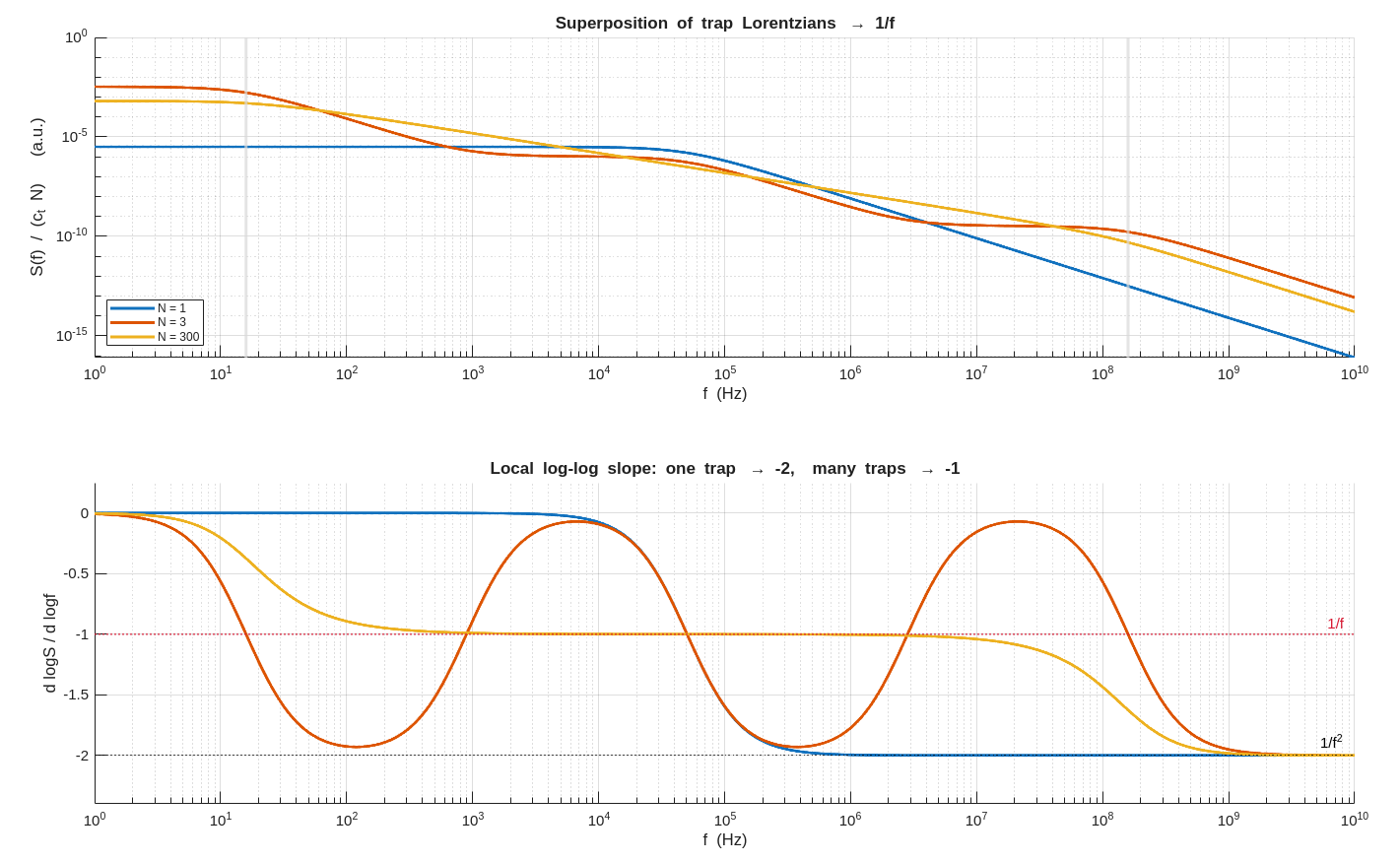
f = logspace(0, 10, 4000); % 1 Hz ... 10 GHz tau_min = 1e-9; % fastest trap (corner ~160 MHz) tau_max = 1e-2; % slowest trap (corner ~16 Hz) r = tau_max/tau_min; % 7 decades of time constants Nlist = [13300]; % number of superposed traps
figure('Color','w','Position',[10060720800]);
% ------------------------------ spectra ------------------------------ ax1 = subplot(2,1,1); hold(ax1,'on'); for m = 1:numel(Nlist) N = Nlist(m); if N == 1 tau = sqrt(tau_min*tau_max); % mid-band trap else tau = logspace(log10(tau_min), log10(tau_max), N); % log-spaced end S = zeros(size(f)); for k = 1:numel(tau) S = S + tau(k) ./ (1 + (2*pi*f*tau(k)).^2); % c_t = 1 end % Every Lorentzian carries the same total power (integral over f = 1/4 % regardless of tau), so dividing by N keeps the total variance fixed: S = S/N; plot(ax1, f, S, 'LineWidth', 2, 'DisplayName', sprintf('N = %d', N)); end
% --------------------------- local slope ----------------------------- ax2 = subplot(2,1,2); hold(ax2,'on'); for m = 1:numel(Nlist) N = Nlist(m); if N == 1 tau = sqrt(tau_min*tau_max); else tau = logspace(log10(tau_min), log10(tau_max), N); end S = zeros(size(f)); for k = 1:numel(tau) S = S + tau(k) ./ (1 + (2*pi*f*tau(k)).^2); end plot(ax2, f, gradient(log(S))./gradient(log(f)), 'LineWidth', 2); end % plot(ax2, f, gradient(log(SL))./gradient(log(f)), '-.', 'Color', [.55 .55 .55]); yline(ax2, -1, ':', '1/f', 'Color', [.85.1.2], 'LineWidth', 1.2); yline(ax2, -2, ':', '1/f^2', 'Color', 'k'); xline(ax2, 1/(2*pi*tau_max), 'Color', [.85.85.85], 'LineWidth', 2); xline(ax2, 1/(2*pi*tau_min), 'Color', [.85.85.85], 'LineWidth', 2); set(ax2, 'XScale', 'log'); grid(ax2,'on'); xlim(ax2, [f(1) f(end)]); ylim(ax2, [-2.40.25]); xlabel(ax2, 'f (Hz)'); ylabel(ax2, 'd logS / d logf'); title(ax2, 'Local log-log slope: one trap \rightarrow -2, many traps \rightarrow -1');
flicker noise upconversion
Y. Hu, T. Siriburanon and R. B. Staszewski, "A Low-Flicker-Noise
30-GHz Class-F23 Oscillator in 28-nm CMOS Using Implicit Resonance and
Explicit Common-Mode Return Path," in IEEE Journal of Solid-State
Circuits, vol. 53, no. 7, pp. 1977-1987, July 2018 [https://ieeexplore.ieee.org/stamp/stamp.jsp?tp=&arnumber=8345650]
—, "Intuitive Understanding of Flicker Noise Reduction via Narrowing
of Conduction Angle in Voltage-Biased Oscillators," in IEEE Transactions
on Circuits and Systems II: Express Briefs, vol. 66, no. 12, pp.
1962-1966, Dec. 2019 [https://sci-hub.se/10.1109/TCSII.2019.2896483]
—, "Oscillator Flicker Phase Noise: A Tutorial," in IEEE
Transactions on Circuits and Systems II: Express Briefs, vol. 68,
no. 2, pp. 538-544, Feb. 2021 [paper]
[slides]
E. G. Ioannidis, C. G. Theodorou, T. A. Karatsori, S. Haendler, C. A.
Dimitriadis and G. Ghibaudo, "Drain-Current Flicker Noise Modeling in
nMOSFETs From a 14-nm FDSOI Technology," in IEEE Transactions on
Electron Devices, vol. 62, no. 5, pp. 1574-1579, May 2015 [https://sci-hub.jp/10.1109/TED.2015.2411678]
Flicker Noise Modulation
MOS flicker noise in large-signal setting can be treated as a
stationary, bias-independent series gate source \(v_{1/f}\) converted to drain current by the
deterministic periodic modulation
its power spectral density is approximately \[
S_{i,1/f}(f)=\frac{K}{|f|}.
\]A large amount of its power lies at low
frequencies. Therefore, compared with a GHz oscillation period
\(T_0\), the flicker-noise value
changes very little during one cycle.
For a flicker-noise component at frequency \(f_m\), \[
f_m T_0\ll 1
\] implies \[
i_{1/f}(t+T_0)\approx i_{1/f}(t).
\] Thus, if the noise current is positive at \(t_0\), it will probably remain positive
throughout the following oscillator cycle: \[
i_{1/f}(t_0+\tau)\approx i_{1/f}(t_0),
\qquad 0\leq \tau<T_0.
\] In circuit-noise analysis, the underlying flicker-noise source
is commonly treated as approximately wide-sense
stationary: \[
R_x(t_1,t_2)=R_x(t_1-t_2).
\] This is reasonable when the device bias is constant and the
measurement interval is finite.
The phase perturbations may cancel or leave a nonzero residual: \[
\Delta\phi_{\text{cycle}}
\propto
\int_{0}^{T_0}
\Gamma(\omega_0 t)\,
i_{1/f,\mathrm{cyclo}}(t)\,dt.
\] Since the low-frequency noise is almost constant over \(T_0\), \[
\Delta\phi_{\text{cycle}}
\approx
x_{1/f}(t_0)
\int_{0}^{T_0}
\Gamma(\omega_0 t)a(t)\,dt
\] Therefore, flicker-noise upconversion depends on whether the
phase-delay and phase-advance contributions cancel over one period. A
nonzero weighted average produces low-frequency fluctuations in
oscillator frequency, which commonly appear as the \(1/f^3\) phase-noise region.
Then \[
\Delta\phi_{\text{cycle}}
\approx
\frac{x_{1/f}(t_0)}{q_{\max}}
\Gamma_{\mathrm{eff,DC}}T_0.
\] If \(x_{1/f}\) is already
normalized by \(q_{\max}\), the \(1/q_{\max}\) factor can be omitted.
Therefore, \[
\boxed{\Gamma_{\mathrm{eff,DC}}=0
\quad\Longrightarrow\quad
\Delta\phi_{\text{cycle}}\approx 0}
\] for quasistatic flicker noise. Physically, the phase-delay
contribution on one edge exactly cancels the phase-advance contribution
on the other edge.nce, \[
\boxed{
\Gamma_{\mathrm{eff,DC}}=0
\Rightarrow
\text{no first-order direct }1/f\text{-to-}1/f^3
\text{ phase-noise upconversion from that source.}
}
\]
A. Demir, A. Mehrotra and J. Roychowdhury, "Phase noise in
oscillators: a unifying theory and numerical methods for
characterization," in IEEE Transactions on Circuits and Systems I:
Fundamental Theory and Applications, vol. 47, no. 5, pp. 655-674,
May 2000 [https://sci-hub.jp/10.1109/81.847872]
—, "A Reliable and Efficient Procedure for Oscillator PPV
Computation, With Phase Noise Macromodeling Applications," IEEE TCAD,
2003.
— and A. Sangiovanni-Vincentelli, Analysis and Simulation of
Noise in Nonlinear Electronic Circuits and Systems, vol. 425.
Boston, MA, USA: Kluwer Academic Publishers, 1998
A. Mehrotra and A. Sangiovanni-Vincentelli, Noise Analysis of
Radio Frequency Circuits, 1st ed. New York, NY, USA: Springer,
2004
Darabi H. Radio Frequency Integrated Circuits and Systems. 2nd ed.
Cambridge University Press; 2020.
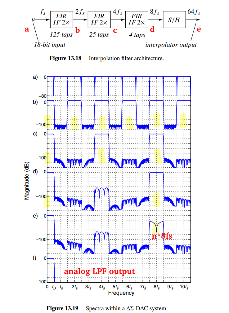
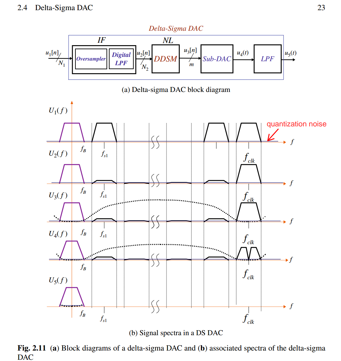
Notice that the requirements of the first stage
are very demanding
replicas suppression
The spectrum of the high resolution digital signal \(u_1\) contains the original
baseband portion and its replicas located at integer
multiples of \(f_{s1}\), plus
a small amount of quantization noise shown as
a solid line
Bourdopoulos, G. I. (2003). Delta-Sigma modulators : modeling,
design and applications. Imperial College Press. [pdf]
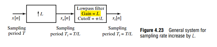
DC Gain in IF
DC gain is used to compensate the ratio of sampling rate before and
after upsample
Given \[
X_e = X = \propto \frac{1}{T} = \frac{1}{L\cdot T_i}
\] Then, the lowpass filter (ZOH, FOH .etc) gain shall be \(L\)
Employ definition of DTFT, \(X(e^{j\hat{\omega}})
=\sum_{n=-\infty}^{+\infty}x[n]e^{-j\hat{\omega} n}\), and set
\(\hat{\omega} = 0\)\[
X(e^{j0}) = \sum_{n=-\infty}^{+\infty}x[n]
\] That is, \(\sum_{n=-\infty}^{+\infty}x[n] =
\sum_{n=-\infty}^{+\infty}x_e[n]\), so \[
\overline{x_e[n]} = \frac{1}{L} \overline{x[n]}
\] It also indicate that dc gain of upsampling is \(1/L\)
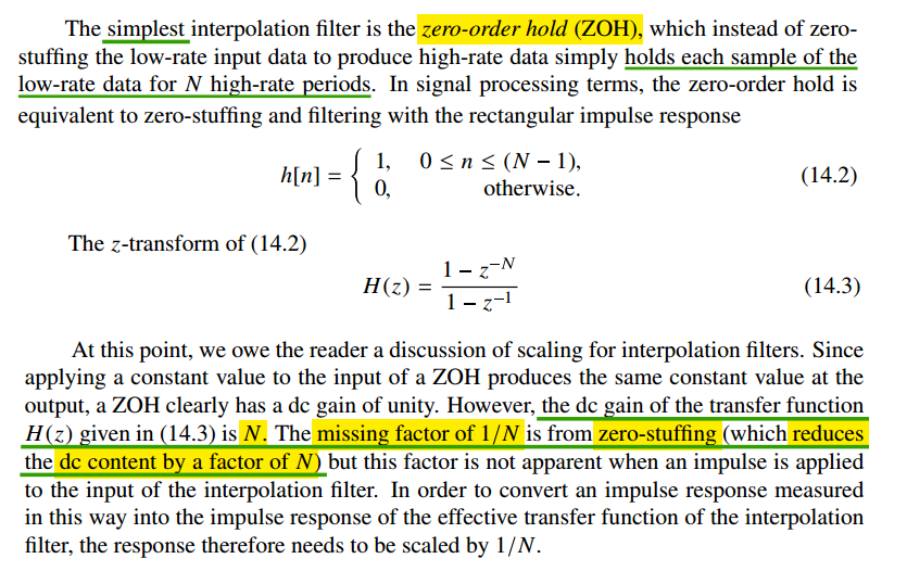
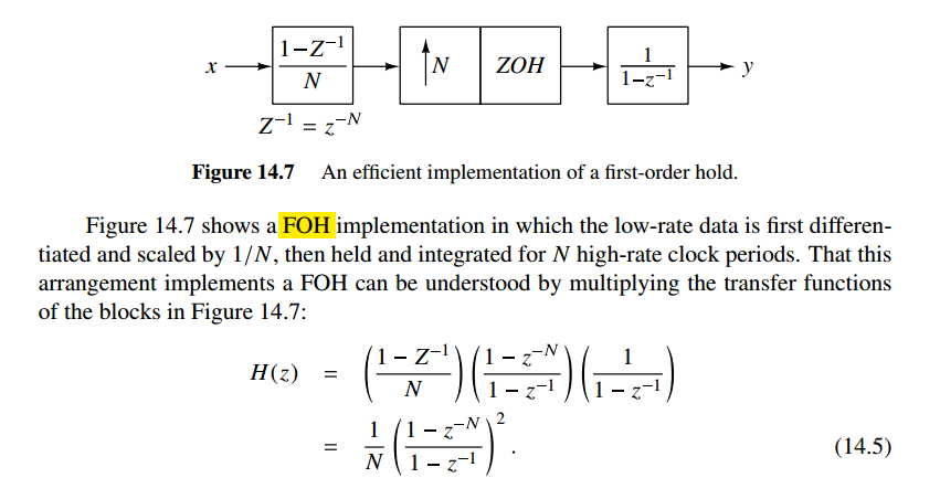
Zero-Order Hold (ZOH)
dc gain = \(N\)
First-Order Hold (FOH)
dc gain = \(N\)
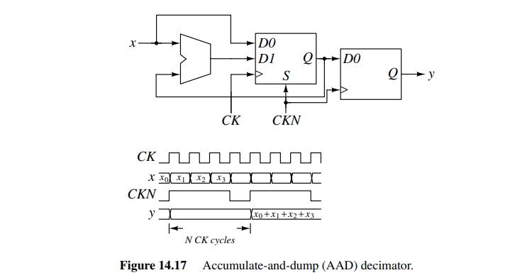
Accumulate-and-dump (AAD)
decimator
accumulating the input for \(N\)
cycles and then latching the result and resetting the integrator
It adds up \(N\) succeeding input
samples at rate \(1/T\) and delivers
their sum in a single sample at the output. Therefore, the
process comprises a filter (in the accumulation) and a
down-sampler (in the dump)
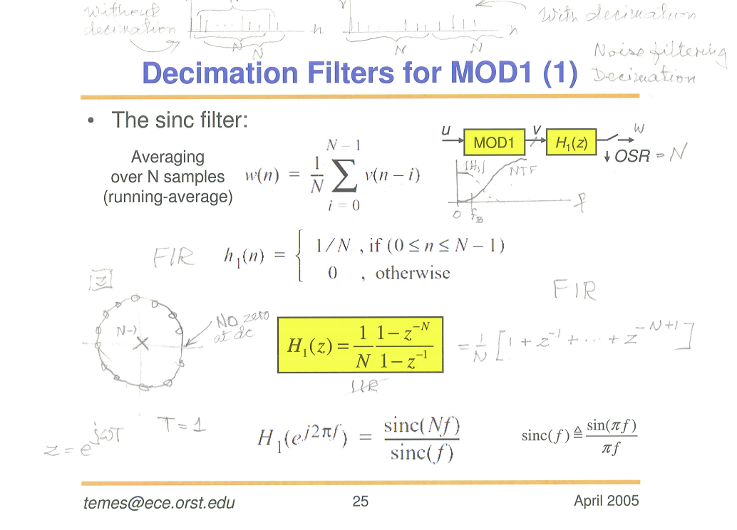
Let's focus on decimation: if we decimate by a factor 4, we simply
retain one output sample out of every 4 input samples.
In the example below, the downsampler at the right drops those 3
samples out of 4, and the output rate, \(y^\prime(n)\), is one fourth of the input
rate \(x(n)\):
with \(z=e^{j\Omega/f_s}\) and \(\xi =z^4\), we have \[
Y^\prime(z) = \frac{1}{4}X(z)\frac{1-z^{-4}}{1-z^{-1}}
\]
But if we're going to be throwing away 75% of the calculated values,
can't we just move the downsampler from the end of the pipeline to
somewhere in the middle? Right between the integrator stage and the comb
stage? That answer is yes, but to keep the math working, we
also need to divide the number of delay elements in the comb stage by
the decimation rate:
with \(z=e^{j\Omega/f_s}\) and \(\xi =z^4\), we have \[
Y^\prime(z) = \frac{1}{4}X(z)\frac{1-z^{-4}}{1-z^{-1}}
\]
And we can do this just the same with cascaded sections (without
downsampler or updampler) where integrators and combs have been
grouped
for decimation, the integrators come first
and the combs second with the downsampler in between
For interpolation, the reverse is true
the incoming sample rate is fraction of the outgoing sample rate,
the combs must come first and the interpolators second
reference
Pavan, Shanthi, Richard Schreier, and Gabor Temes. (2016) 2016.
Understanding Delta-Sigma Data Converters. 2nd ed. Wiley.
K. Hosseini and M. P. Kennedy, Minimizing Spurious Tones in Digital
Delta-Sigma Modulators (Analog Circuits and Signal Processing). New
York, NY, USA: Springer, 2011.