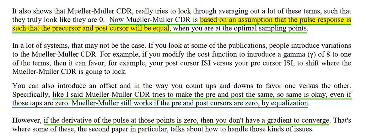
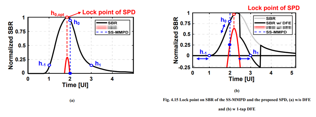
A dynamical system can be linear or nonlinear. Independently, it can be deterministic or stochastic. Continuous-time deterministic systems are commonly modeled by ODEs, while continuous-time stochastic systems are commonly modeled by SDEs

Deterministic Stochastic
Linear Linear ODE Linear SDE
Nonlinear Nonlinear ODE Nonlinear SDE

The two classifications answer different questions:

  • Linear/nonlinear: How does the state enter the evolution equation?
  • Deterministic/stochastic: Does the evolution include randomness?

For Demir’s oscillator theory, however, the main path is \[ \boxed{ \text{nonlinear deterministic ODE} \rightarrow \text{add device noise} \rightarrow \text{nonlinear SDE} } \]

instantaneous & average PSD

For white noise \(n(t)\)
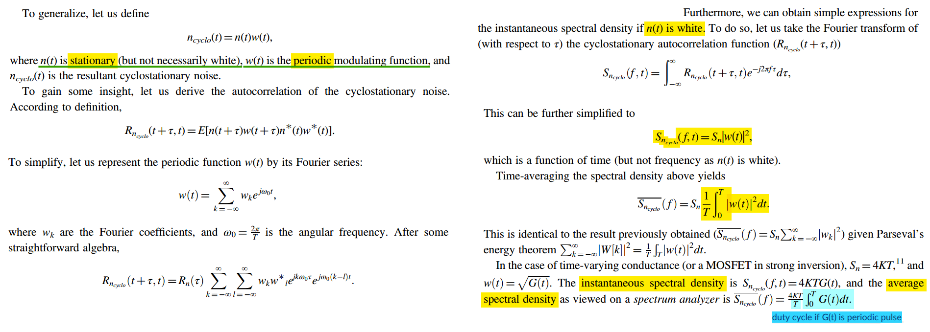
image-20260725005940162

flicker noise Modulation

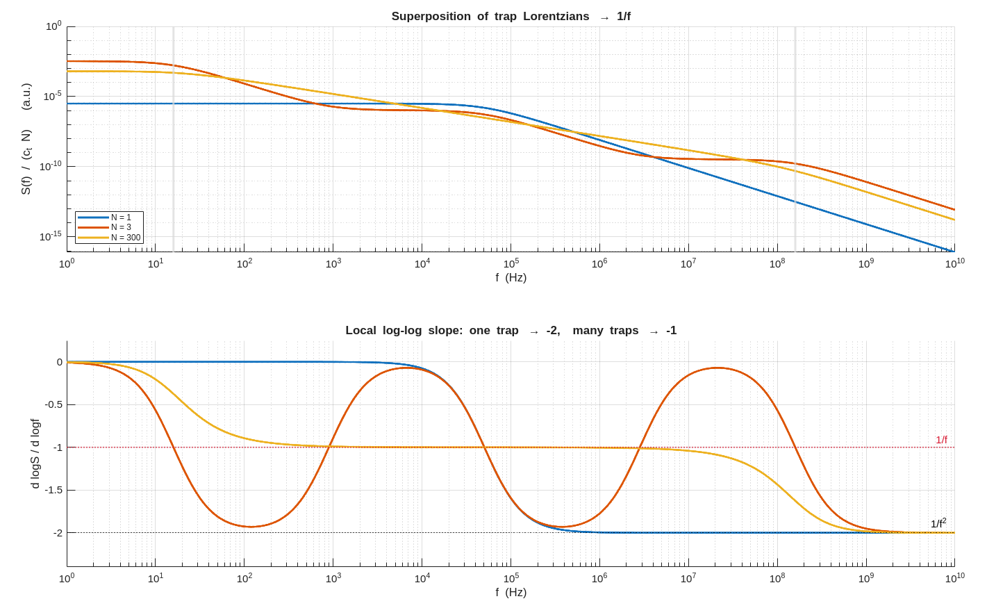
flicker noise spectrum
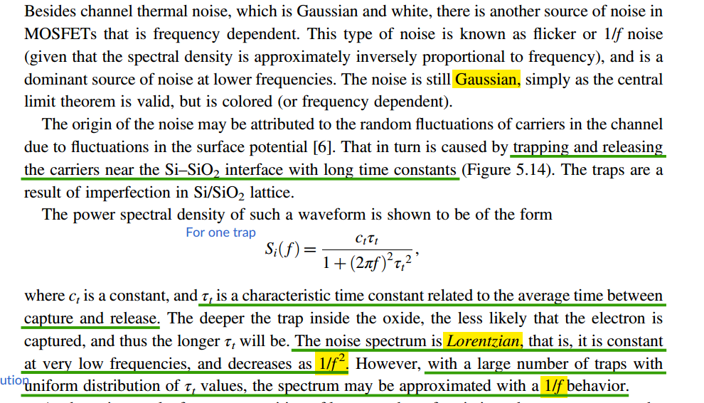
image-20260724230315724

image-20260724230516271

1
2
3
4
5
6
7
8
9
10
11
12
13
14
15
16
17
18
19
20
21
22
23
24
25
26
27
28
29
30
31
32
33
34
35
36
37
38
39
40
41
42
43
44
45
46
47
48
49
50
51
52
53
54
55
56
57
58
59
f       = logspace(0, 10, 4000);      % 1 Hz ... 10 GHz
tau_min = 1e-9; % fastest trap (corner ~160 MHz)
tau_max = 1e-2; % slowest trap (corner ~16 Hz)
r = tau_max/tau_min; % 7 decades of time constants
Nlist = [1 3 300]; % number of superposed traps

figure('Color','w','Position',[100 60 720 800]);

% ------------------------------ spectra ------------------------------
ax1 = subplot(2,1,1); hold(ax1,'on');
for m = 1:numel(Nlist)
N = Nlist(m);
if N == 1
tau = sqrt(tau_min*tau_max); % mid-band trap
else
tau = logspace(log10(tau_min), log10(tau_max), N); % log-spaced
end
S = zeros(size(f));
for k = 1:numel(tau)
S = S + tau(k) ./ (1 + (2*pi*f*tau(k)).^2); % c_t = 1
end
% Every Lorentzian carries the same total power (integral over f = 1/4
% regardless of tau), so dividing by N keeps the total variance fixed:
S = S/N;
plot(ax1, f, S, 'LineWidth', 2, 'DisplayName', sprintf('N = %d', N));
end

xline(ax1, 1/(2*pi*tau_max), 'Color', [.85 .85 .85], 'LineWidth',2, 'HandleVisibility', 'off');
xline(ax1, 1/(2*pi*tau_min), 'Color', [.85 .85 .85], 'LineWidth',2, 'HandleVisibility', 'off');
set(ax1, 'XScale','log', 'YScale','log'); grid(ax1,'on');
xlim(ax1, [f(1) f(end)]);
xlabel(ax1, 'f (Hz)'); ylabel(ax1, 'S(f) / (c_t N) (a.u.)');
title(ax1, 'Superposition of trap Lorentzians \rightarrow 1/f');
legend(ax1, 'Location', 'southwest', 'FontSize', 8);

% --------------------------- local slope -----------------------------
ax2 = subplot(2,1,2); hold(ax2,'on');
for m = 1:numel(Nlist)
N = Nlist(m);
if N == 1
tau = sqrt(tau_min*tau_max);
else
tau = logspace(log10(tau_min), log10(tau_max), N);
end
S = zeros(size(f));
for k = 1:numel(tau)
S = S + tau(k) ./ (1 + (2*pi*f*tau(k)).^2);
end
plot(ax2, f, gradient(log(S))./gradient(log(f)), 'LineWidth', 2);
end
% plot(ax2, f, gradient(log(SL))./gradient(log(f)), '-.', 'Color', [.55 .55 .55]);
yline(ax2, -1, ':', '1/f', 'Color', [.85 .1 .2], 'LineWidth', 1.2);
yline(ax2, -2, ':', '1/f^2', 'Color', 'k');
xline(ax2, 1/(2*pi*tau_max), 'Color', [.85 .85 .85], 'LineWidth', 2);
xline(ax2, 1/(2*pi*tau_min), 'Color', [.85 .85 .85], 'LineWidth', 2);
set(ax2, 'XScale', 'log'); grid(ax2,'on');
xlim(ax2, [f(1) f(end)]); ylim(ax2, [-2.4 0.25]);
xlabel(ax2, 'f (Hz)'); ylabel(ax2, 'd logS / d logf');
title(ax2, 'Local log-log slope: one trap \rightarrow -2, many traps \rightarrow -1');

numerical generation of flicker noise

Bibbona, Enrico, Gianna Panfilo and Patrizia Tavella. "The Ornstein–Uhlenbeck process as a model of a low pass filtered white noise." Metrologia 45 (2008): S117 - S126. [https://iris.polito.it/retrieve/e384c42f-3847-d4b2-e053-9f05fe0a1d67/OUasFWN_finale.pdf]

Ornstein–Uhlenbeck process, equivalently white noise passed through a first-order low-pass filter
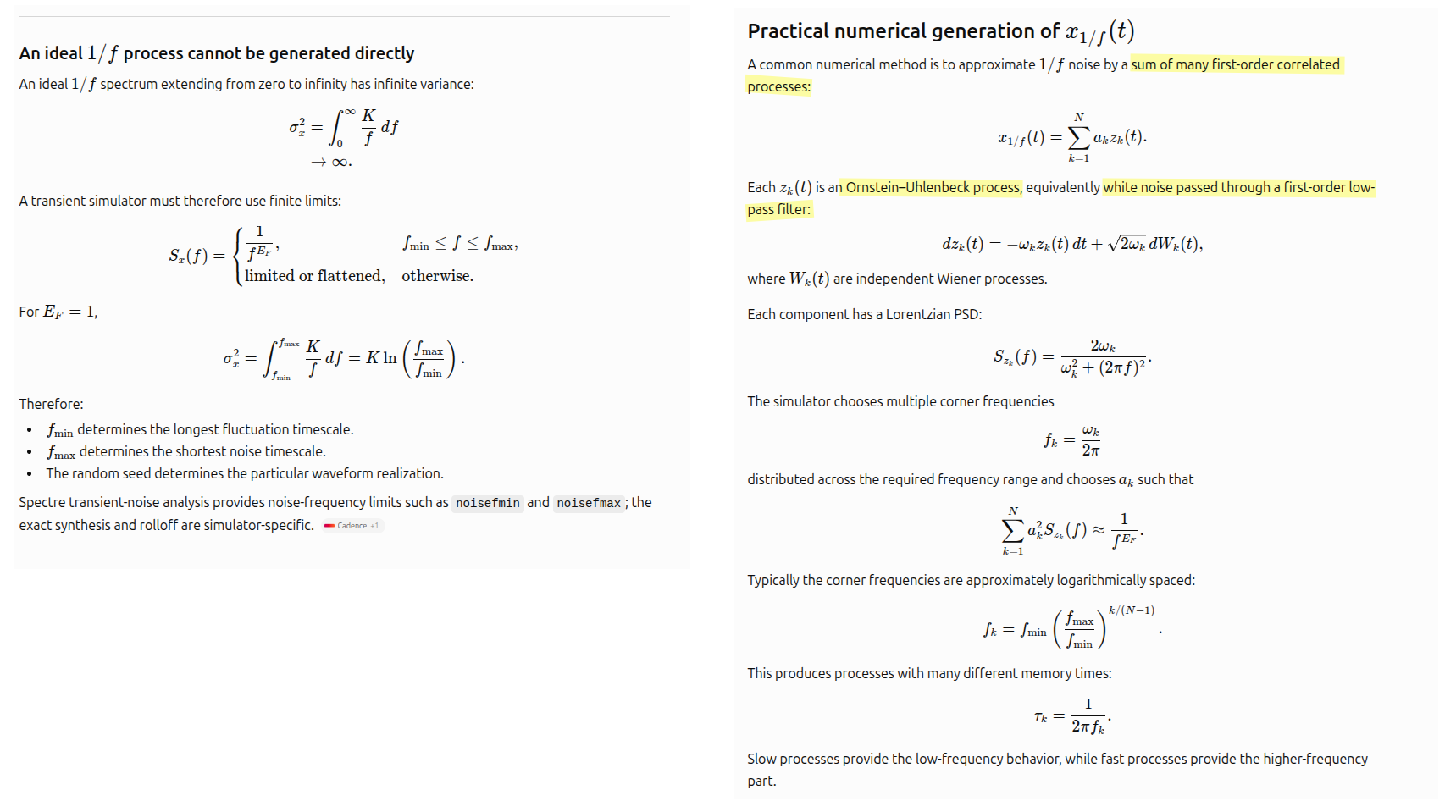
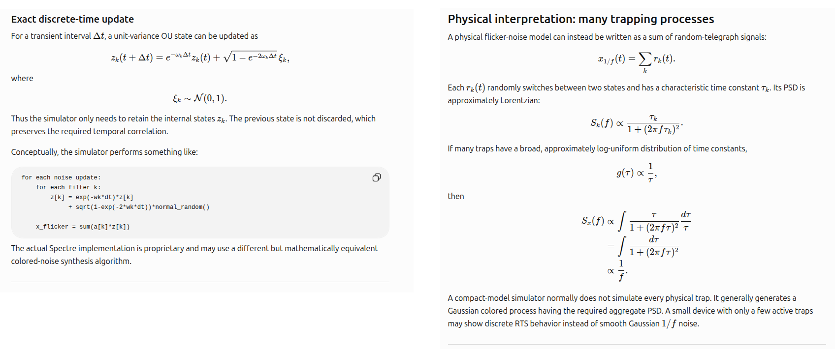
image-20260801203350117

image-20260801203516575

Flicker Noise Formulations in Verilog-A

G. J. Coram, C. C. McAndrew, K. K. Gullapalli and K. S. Kundert, "Flicker Noise Formulations in Compact Models," in IEEE Transactions on Computer-Aided Design of Integrated Circuits and Systems, vol. 39, no. 10, pp. 2812-2821, Oct. 2020 [https://kenkundert.com/docs/tcad20-flicker-noise.pdf],[https://github.com/KenKundert/flicker-noise]

BSIM4v4.7 MOSFET Model -User's Manual [https://class.ece.iastate.edu/djchen/ee501/BSIM470_Manual.pdf]

C. C. McAndrew et al., "Best Practices for Compact Modeling in Verilog-A," in IEEE Journal of the Electron Devices Society, vol. 3, no. 5, pp. 383-396, Sept. 2015 [https://ieeexplore.ieee.org/stamp/stamp.jsp?arnumber=7154394]
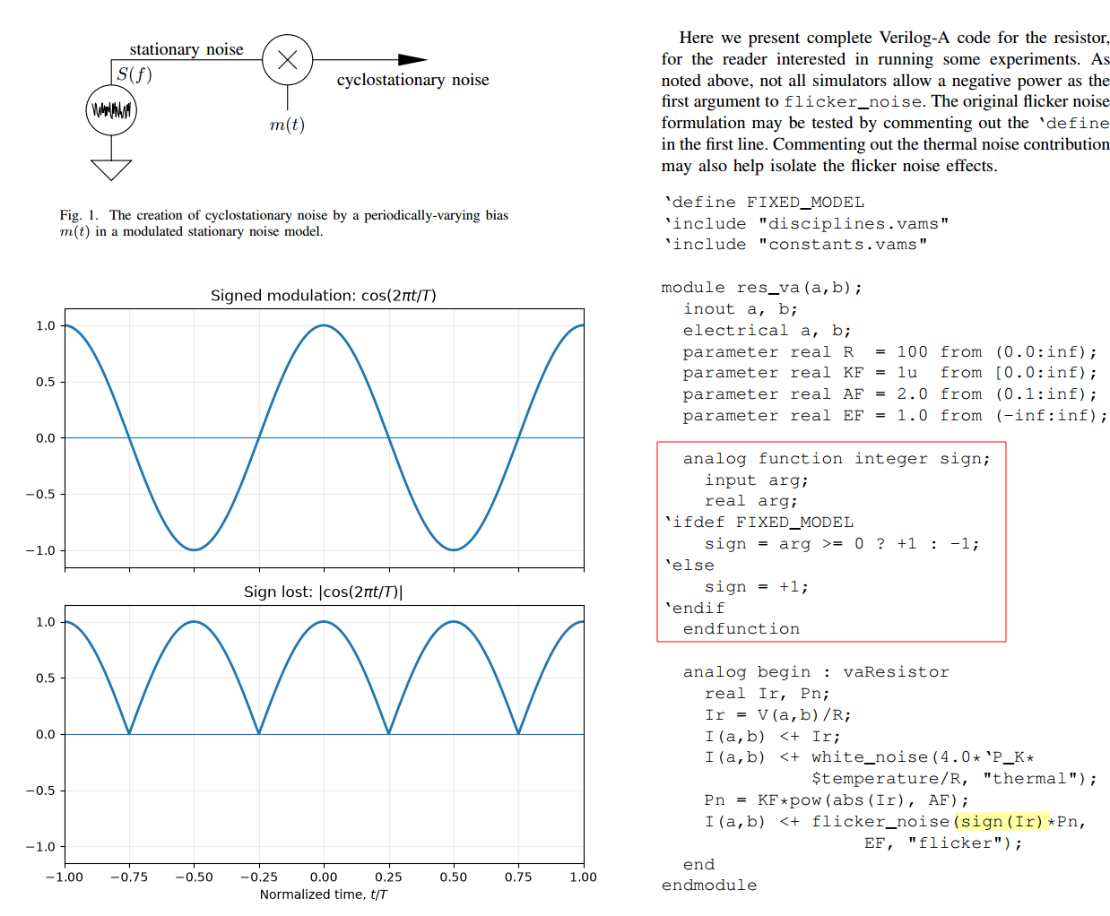
image-20260801190953551

When sign(Ir) = -1, the argument becomes \[ q(t)=\operatorname{sign}(I_r)P_n=-P_n. \] A simulator that correctly supports Kundert’s formulation does not interpret this as a physically negative PSD, nor does it calculate the ordinary complex square root \(\sqrt{-P_n}\). Instead, the sign selects the sign of the deterministic noise-modulation amplitude: \[ \boxed{ m(t)=\operatorname{sign}\!\big(q(t)\big)\sqrt{|q(t)|} } \] Therefore, when \(q=-P_n\), \[ m(t)=-\sqrt{P_n}. \] This is equivalent to

1
I(a,b) <+ sign(Ir)*flicker_noise(Pn, EF, "flicker");

provided the simulator supports a noise function inside an expression
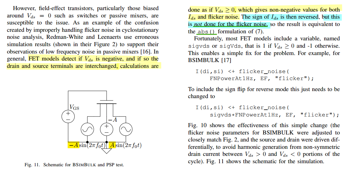
image-20260802114438747

flicker_noise_commutation_vs_abs_static

1
2
3
4
5
6
7
8
9
10
11
12
13
14
15
16
17
18
19
20
21
22
23
24
// BSIM flicker noise simulations

simulator lang=spectre

model nchbsim4_f0 bsim4 fnoimod=0 kf=1e-23 af=2
model nchbsim4_f1 bsim4 fnoimod=1

Vmod (mod 0) vsource type=sine dc=1.0 sinedc=0.0 ampl=100mV freq=131.072kHz
ED (d 0 mod 0) vcvs gain=1
ES (s 0 mod 0) vcvs gain=-1
VG (g 0) vsource dc=3
VB (b 0) vsource dc=-0.2

MBSIM4f0 (d_f0 g s b) nchbsim4_f0 l=1um w=10um
MBSIM4f1 (d_f1 g s b) nchbsim4_f1 l=1um w=10um

iRESf0 (d d_f0) vsource dc=0.0
iRESf1 (d d_f1) vsource dc=0.0
Rout (noise 0) resistor isnoisy=no r=100kOhm
Hnoise (noise 0) pccvs coeffs=[0 1 1] probes=[iRESf0 iRESf1]

noise (noise 0) noise start=4_Hz stop=4.194304MHz dec=2k
pop pss fund=131.072kHz
pnoise (noise 0) pnoise start=4_Hz stop=4.194304MHz dec=2k maxsideband=10
1
2
3
4
5
6
7
8
9
10
11
12
13
14
15
// Resistor flicker noise simulations

simulator lang=spectre

ahdl_include "resistor.va"

model rref resistor kf=1.0e-6 af=2 // to match res_va

Vmod (n 0) vsource type=sine dc=1.0 sinedc=0.0 ampl=100mV freq=131.072kHz
Rva (n 0) res_va
Rref (n 0) rref r=100.0

noise noise start=4_Hz stop=4.194304MHz dec=2k oprobe=Vmod
pss pss fund=131.072kHz maxacfreq=4.194304MHz
pnoise pnoise start=4_Hz stop=4.194304MHz dec=2k maxsideband=10 oprobe=Vmod

Marek Mierzwinski, Verilog-A Standardization for Compact Modeling [https://www.mos-ak.org/washington_dc/papers/Mierzwinski_MOS-AK_2011.pdf]

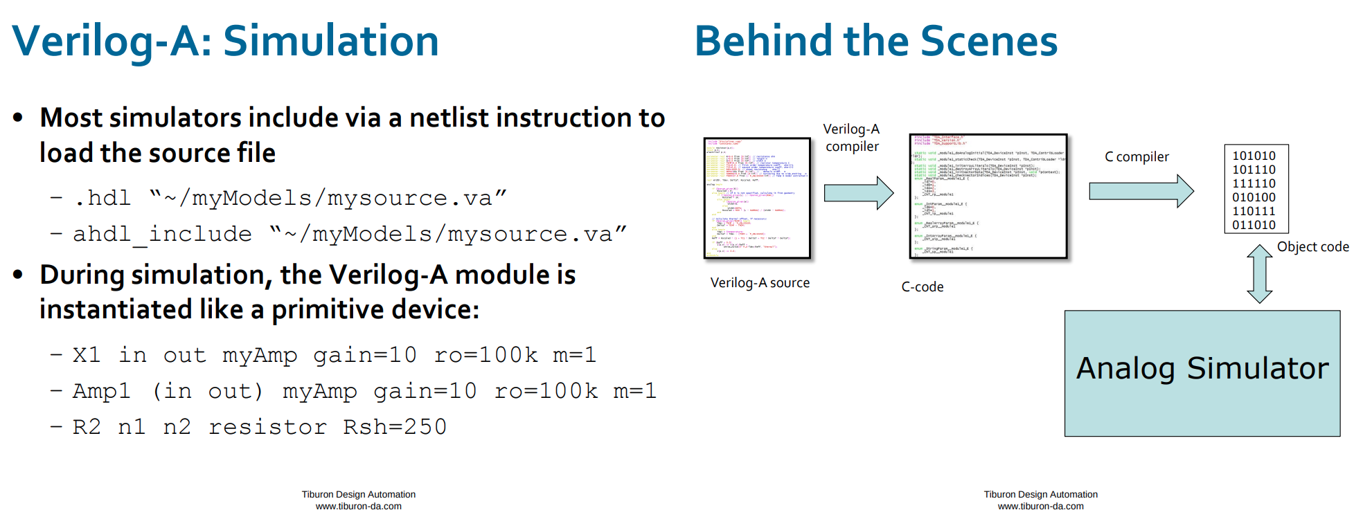
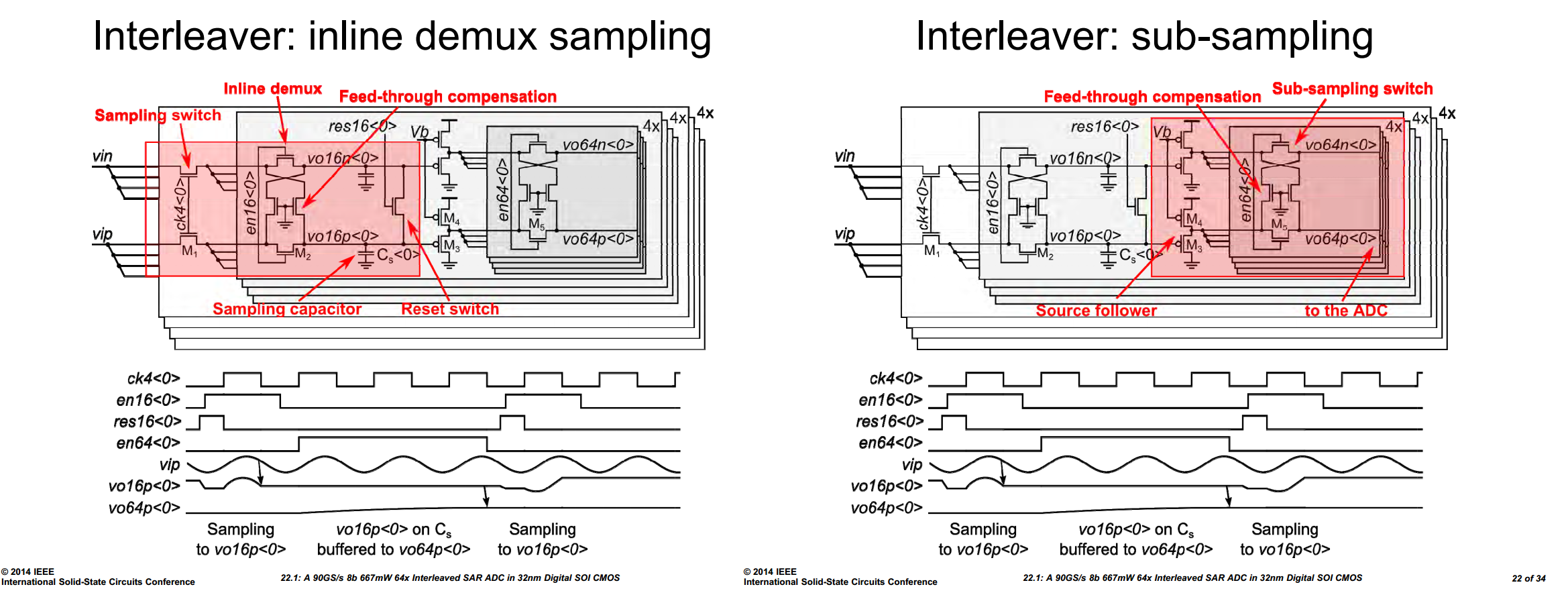
Current BSIM models use compact-model equations standardized through reference Verilog-A code, but commercial simulators often execute an optimized built-in implementation rather than the Verilog-A source directly
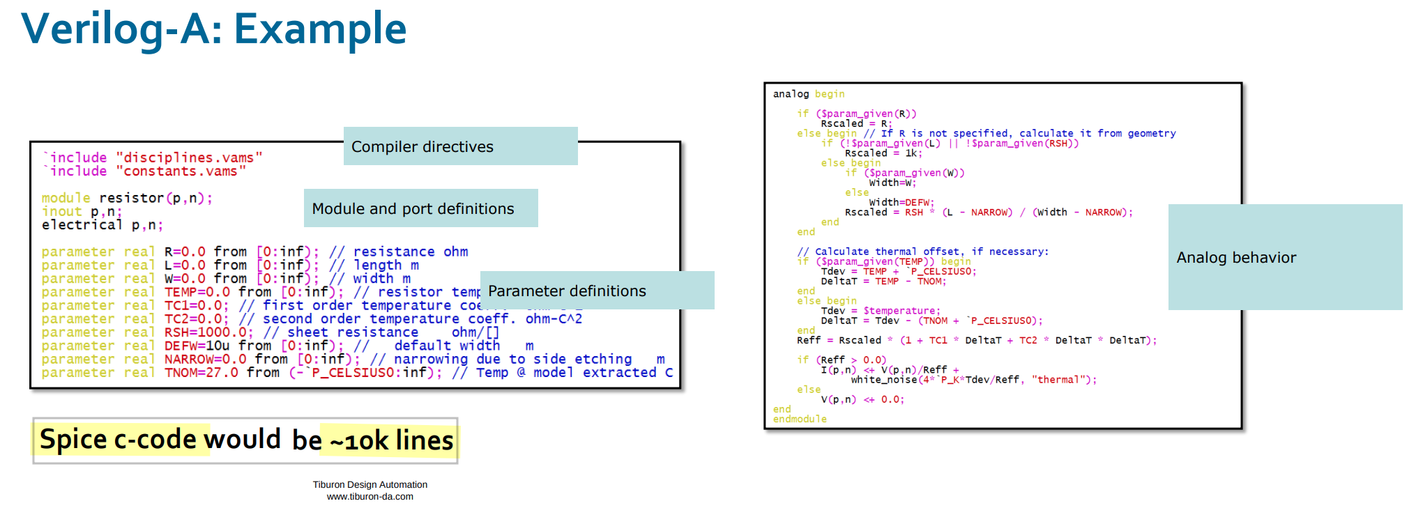
image-20260729232946151

image-20260729233151017

image-20260729233304135

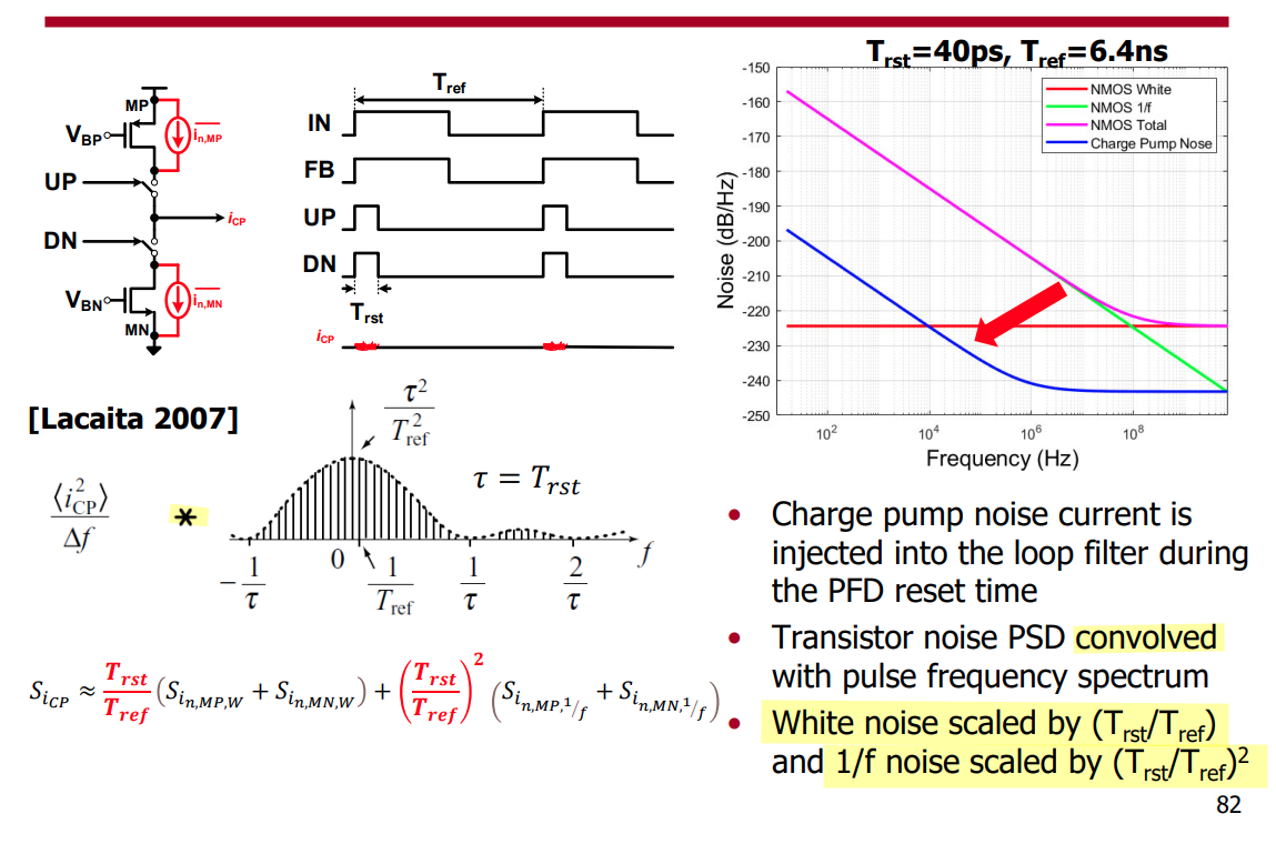
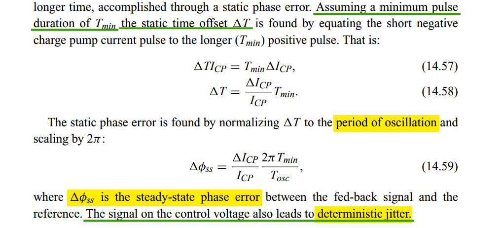
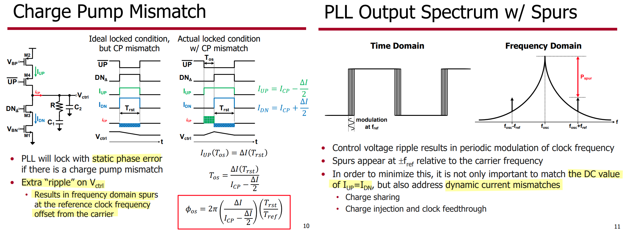
flicker noise in circuit-noise analysis

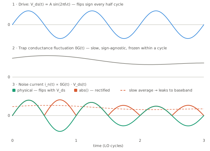
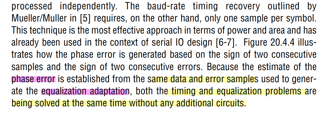
its power spectral density is approximately \[ S_{i,1/f}(f)=\frac{K}{|f|}. \] A large amount of its power lies at low frequencies. Therefore, compared with a GHz oscillation period \(T_0\), the flicker-noise value changes very little during one cycle.

For a flicker-noise component at frequency \(f_m\), \[ f_m T_0\ll 1 \] implies \[ i_{1/f}(t+T_0)\approx i_{1/f}(t). \] Thus, if the noise current is positive at \(t_0\), it will probably remain positive throughout the following oscillator cycle: \[ i_{1/f}(t_0+\tau)\approx i_{1/f}(t_0), \qquad 0\leq \tau<T_0. \] In circuit-noise analysis, the underlying flicker-noise source is commonly treated as approximately wide-sense stationary: \[ R_x(t_1,t_2)=R_x(t_1-t_2). \] This is reasonable when the device bias is constant and the measurement interval is finite.

The phase perturbations may cancel or leave a nonzero residual: \[ \Delta\phi_{\text{cycle}} \propto \int_{0}^{T_0} \Gamma(\omega_0 t)\, i_{1/f,\mathrm{cyclo}}(t)\,dt. \] Since the low-frequency noise is almost constant over \(T_0\), \[ \Delta\phi_{\text{cycle}} \approx x_{1/f}(t_0) \int_{0}^{T_0} \Gamma(\omega_0 t)a(t)\,dt \] Therefore, flicker-noise upconversion depends on whether the phase-delay and phase-advance contributions cancel over one period. A nonzero weighted average produces low-frequency fluctuations in oscillator frequency, which commonly appear as the \(1/f^3\) phase-noise region.

Define

\[ \Gamma_{\mathrm{eff,DC}}\equiv \frac{1}{T_0}\int_0^{T_0}\Gamma(\omega_0t)a(t)\,dt \]

Then \[ \Delta\phi_{\text{cycle}} \approx \frac{x_{1/f}(t_0)}{q_{\max}} \Gamma_{\mathrm{eff,DC}}T_0. \] If \(x_{1/f}\) is already normalized by \(q_{\max}\), the \(1/q_{\max}\) factor can be omitted.

Therefore, \[ \boxed{\Gamma_{\mathrm{eff,DC}}=0 \quad\Longrightarrow\quad \Delta\phi_{\text{cycle}}\approx 0} \] for quasistatic flicker noise. Physically, the phase-delay contribution on one edge exactly cancels the phase-advance contribution on the other edge.nce, \[ \boxed{ \Gamma_{\mathrm{eff,DC}}=0 \Rightarrow \text{no first-order direct }1/f\text{-to-}1/f^3 \text{ phase-noise upconversion from that source.} } \]

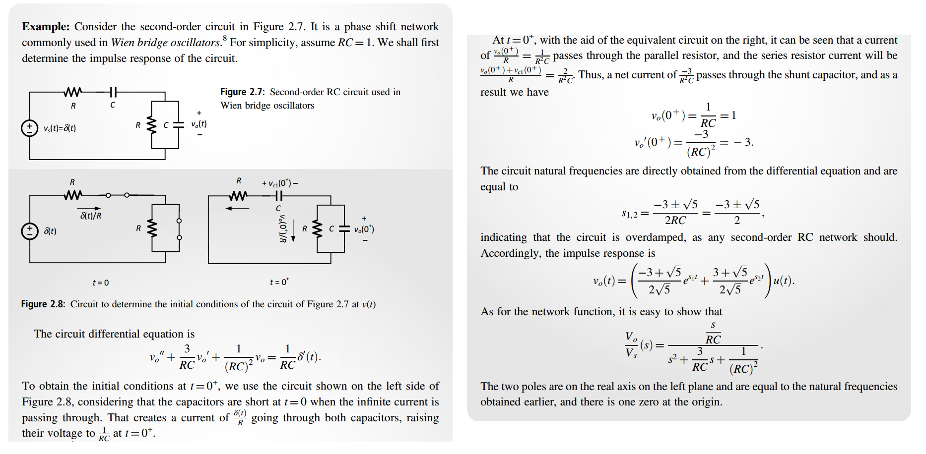
Ordinary Differential Equations (ODEs)

Steve Brunton, ME 564 - Mechanical Engineering Analysis [http://faculty.washington.edu/sbrunton/me564/] [videos]

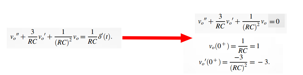
Dirac delta function in ODEs

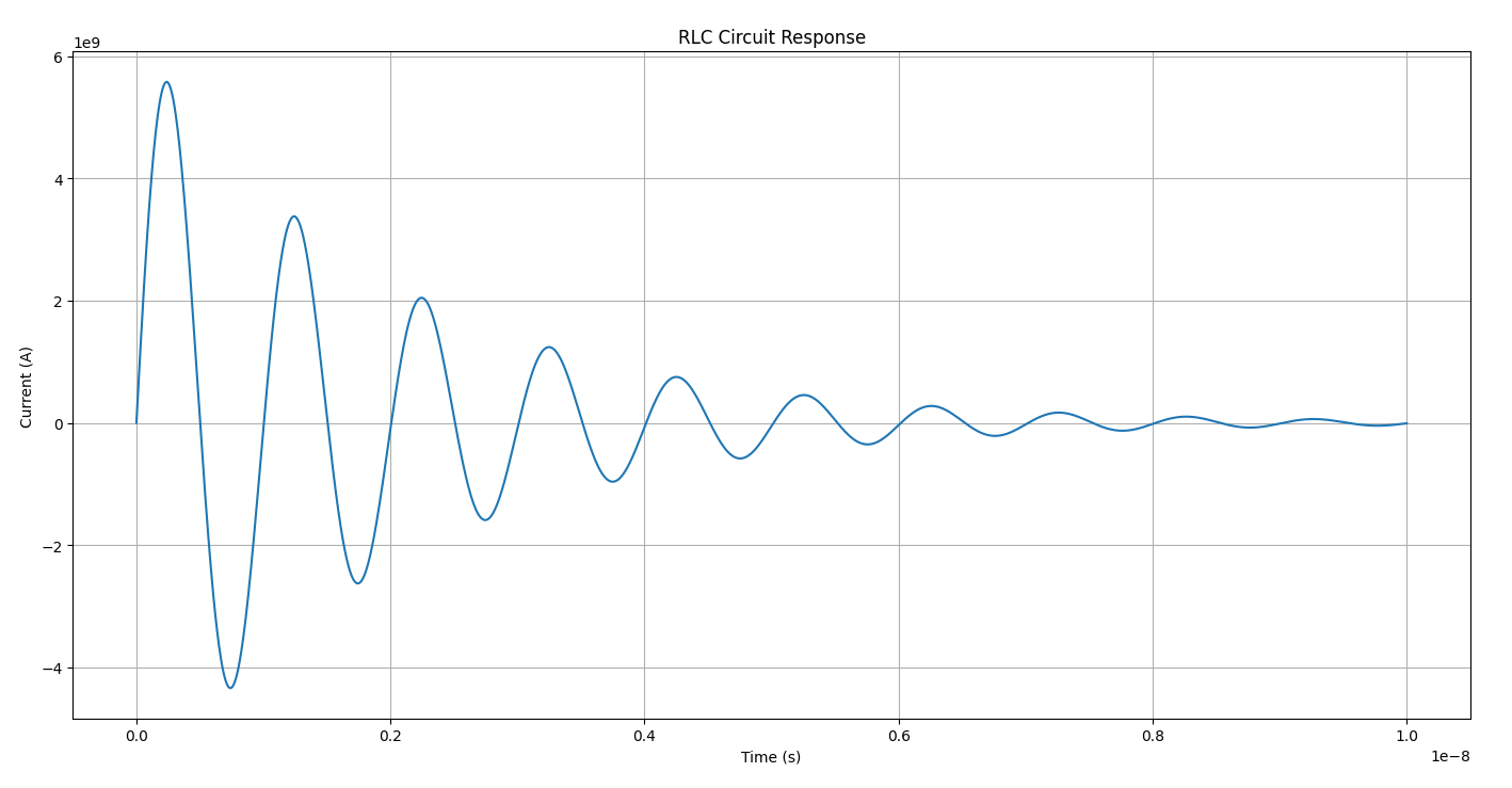
Integrate across the impulse to find the jump \[ \underbrace{\text{zero state} + \delta(t)\text{ input}}_{t=0^-} \quad\Longrightarrow\quad \underbrace{\text{zero input} + \text{new ICs at }t=0^+}_{t>0} \]
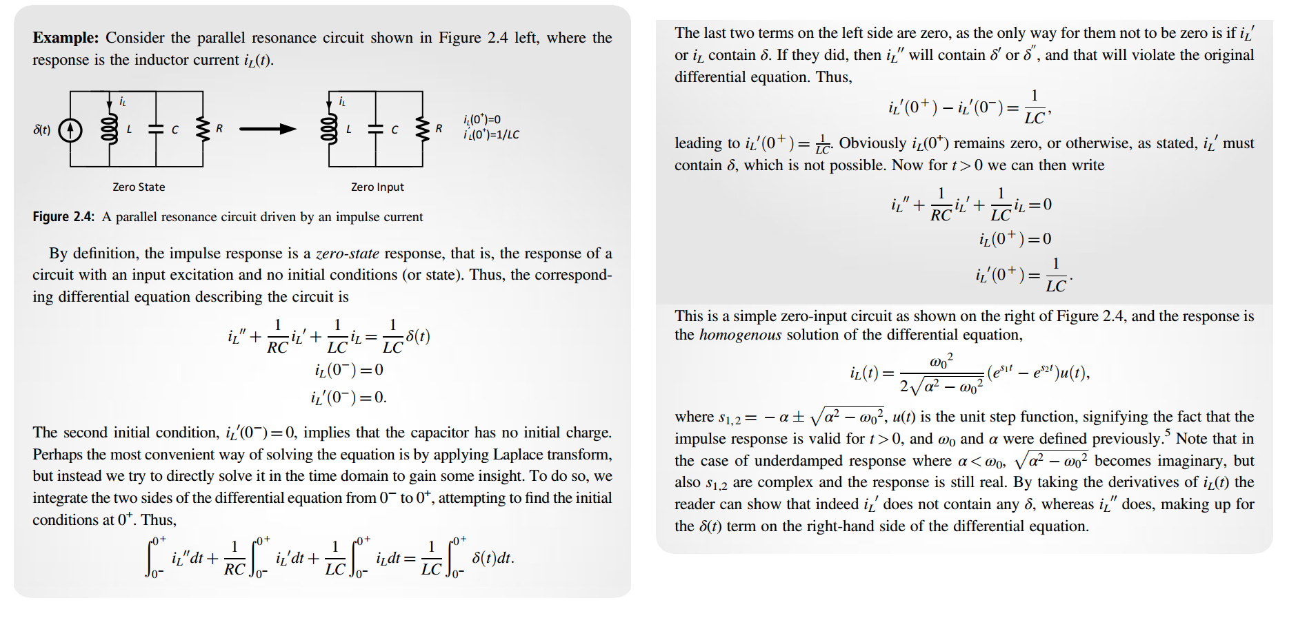
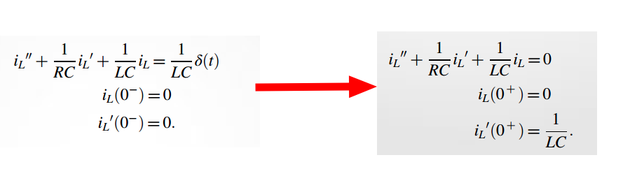
image-20260710230815001

image-20260711003430785

1
2
3
4
5
6
7
8
9
10
11
12
13
14
15
16
17
18
19
20
21
22
23
import numpy as np
import scipy.integrate as spi
import matplotlib.pyplot as plt


L, C, R = 2.533e-9, 10e-12, 100.0

def rhs(t, y):
il , dil = y
dildt = dil
ddildt = -(1/(R*C))*dil - (1/(L*C))*il
return [dildt, ddildt]

sol = spi.solve_ivp(rhs, (0, 10e-9), [0, 1/(L*C)],
t_eval=np.linspace(0, 10e-9, 2001),
rtol=1e-10, atol=1e-4) # error drops to ~1e-10

plt.plot(sol.t, sol.y[0])
plt.title('RLC Circuit Response')
plt.xlabel('Time (s)')
plt.ylabel('Current (A)')
plt.grid()
plt.show()

image-20260710235118022

Doublet function in ODEs

image-20260711004412242

image-20260711004554172

image-20260711010924471

1
2
3
4
5
6
7
8
9
10
11
12
13
14
15
16
17
18
19
20
21
22
23
24
25
26
27
28
29
30
31
32
33
34
35
36
37
38
39
40
41
42
43
44
45
46
47
48
49
50
51
52
53
54
55
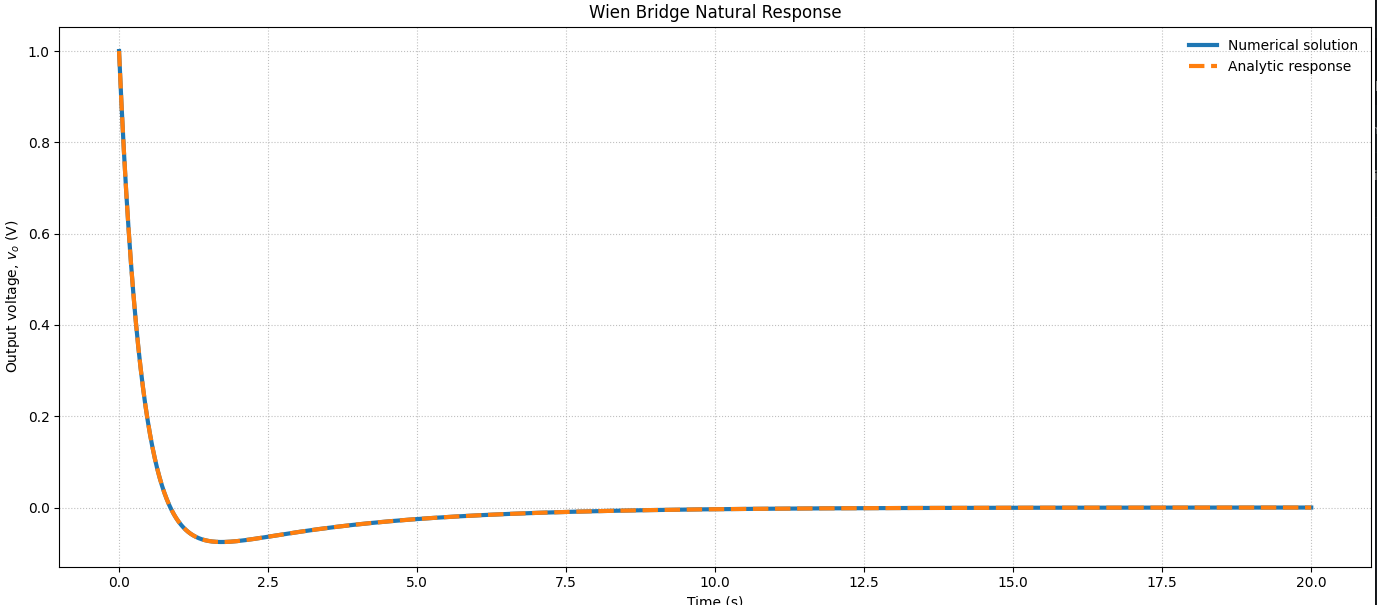
import numpy as np
import scipy.integrate as spi
import matplotlib.pyplot as plt


RC = 1.0
T_START = 0.0
T_STOP = 20.0
NUM_SAMPLES = 2001


def wien_bridge_rhs(t, state):
"""Return the state derivative for the normalized Wien bridge response."""
#del t
vo, dvo = state
ddvo = -(3.0 / RC) * dvo - vo / RC**2
return [dvo, ddvo]


def analytic_response(t):
"""Closed-form voltage response for the same initial conditions."""
sqrt_5 = np.sqrt(5.0)
s1 = (-3.0 + sqrt_5) / (2.0 * RC)
s2 = (-3.0 - sqrt_5) / (2.0 * RC)
return (s1 * np.exp(s1 * t) - s2 * np.exp(s2 * t)) / sqrt_5


def main():
t_eval = np.linspace(T_START, T_STOP, NUM_SAMPLES)
initial_state = [1.0 / RC, -3.0 / RC**2]

sol = spi.solve_ivp(
wien_bridge_rhs,
(T_START, T_STOP),
initial_state,
t_eval=t_eval,
rtol=1e-10,
atol=1e-8,
)

fig, ax = plt.subplots(figsize=(8, 4.8), constrained_layout=True)
ax.plot(sol.t, sol.y[0], linewidth=3.0, label="Numerical solution")
ax.plot(t_eval, analytic_response(t_eval), "--", linewidth=3.0, label="Analytic response")

ax.set_title("Wien Bridge Natural Response")
ax.set_xlabel("Time (s)")
ax.set_ylabel("Output voltage, $v_o$ (V)")
ax.grid(True, which="both", linestyle=":", linewidth=0.8, alpha=0.8)
ax.legend(frameon=False)

plt.show()


if __name__ == "__main__":
main()

Stochastic Differential Equations (SDE)

TODO 📅

Fourier Analysis & Partial Differential Equations (PDEs)

\[ \text{Fourier analysis} \longrightarrow \text{method for solving PDEs}, \]

TODO 📅

Differential Equations in Matlab & Python

scipy.integrate.solve_ivp

Solve an initial value problem for a system of ODEs

rtol and atol are the error tolerances for scipy.integrate.solve_ivp.

rtol is relative tolerance: allowed error scales with the size of the solution.

atol is absolute tolerance: allowed error floor when the solution is near zero.

SciPy roughly controls local error using:

1
error < atol + rtol * abs(y)

DifferentialEquations.jl

ODE forms

ODE is usually defined in one of two forms: out-of-place or in-place

1
2
3
4
5
6
7
8
9
10
11
# out-of-place

function f(x, p, t)
return 2x
end

x0 = 1.0
tspan = (0.0, 5.0)

prob = ODEProblem(f, x0, tspan)
sol = solve(prob)

x = current state

p = parameters

t = current time

returned value = dx/dt

1
2
3
4
5
6
7
8
9
10
11
# in-place

function f!(dx, x, p, t)
dx[1] = 2*x[1] # calars cannot be mutated
end

x0 = [1.0]
tspan = (0.0, 5.0)

prob = ODEProblem(f!, x0, tspan)
sol = solve(prob)

Scalar ODE \[ \frac{dx}{dt} = -2x \]

1
2
3
4
5
6
7
8
9
function f(x, p, t)
return 2x
end

x0 = 1.0
tspan = (0.0, 5.0)

prob = ODEProblem(f, x0, tspan)
sol = solve(prob)

System of ODEs

\[\begin{align} \dot{x} &= y, \\ \dot{y} &= -x - 0.2y. \end{align}\]

1
2
3
4
5
6
7
8
9
10
11
12
13
function oscillator!(du, u, p, t)
x = u[1]
y = u[2]

du[1] = y
du[2] = -x - 0.2y
end

u0 = [1.0, 0.0]
tspan = (0.0, 20.0)

prob = ODEProblem(oscillator!, u0, tspan)
sol = solve(prob)

\[ u = \begin{bmatrix} x \\ y \end{bmatrix}, \quad du = \begin{bmatrix} \dot{x} \\ \dot{y} \end{bmatrix}. \]

ODE with parameters

1
2
3
4
5
6
7
8
9
10
11
12
13
function f!(du, u, p, t)
a, b = p
x = u[1]

du[1] = a*x - b*x^3
end

u0 = [0.1]
p = (2.0, 1.0)
tspan = (0.0, 10.0)

prob = ODEProblem(f!, u0, tspan, p)
sol = solve(prob)

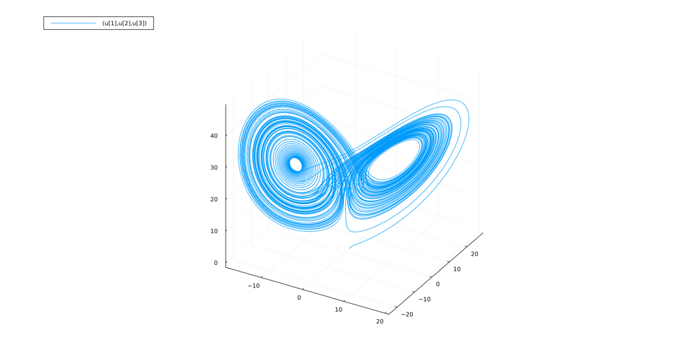
The Lorenz Equation — employ above features

\[\begin{align} \frac{dx}{dt} &= \sigma (y - x) \\ \frac{dy}{dt} &= x (\rho - z) -y \\ \frac{dz}{dt} &= xy - \beta z \end{align}\]

1
2
3
4
5
6
7
8
9
10
11
12
13
14
15
function lorenz!(du,u,p,t)
σ,ρ,β = p
du[1] = σ*(u[2]-u[1])
du[2] = u[1]*(ρ-u[3]) - u[2]
du[3] = u[1]*u[2] - β*u[3]
end

u0 = [1.0,0.0,0.0]
p = (10,28,8/3) # we could also make this an array, or any other type!
tspan = (0.0,100.0)

prob = ODEProblem(lorenz!,u0,tspan,p)
sol = solve(prob)

Plots.plot(sol, vars=(1,2,3), size=(1400, 700))

image-20260815142842589

Event Handling & Callback Functions

In DifferentialEquations.jl, a callback allows the ODE solver to detect an event and execute some action when that event occurs. This is useful for hybrid systems, switching circuits, threshold detection, impacts, resets, stopping conditions, etc. \[ \boxed{\text{condition} \longrightarrow \text{event} \longrightarrow \text{affect!}} \]

Callback Condition Typical use
ContinuousCallback (g(u,t)=0) zero crossings, thresholds, impacts
DiscreteCallback Boolean mode switching, logical conditions
1
2
3
4
5
6
7
8
9
10
11
12
13
14
15
16
17
18
19
20
21
22
23
24
25
26
27
28
29
function f!(du, u, p, t)
du[1] = -u[1]
end

u0 = [1.0]
tspan = (0.0, 10.0)

prob = ODEProblem(f!, u0, tspan)

function condition(u, t, integrator)
u[1] - 0.2
end

function affect!(integrator)
terminate!(integrator)
end

cb = ContinuousCallback(condition, affect!)

sol = solve(prob, Tsit5(), callback=cb)
println(sol.u[end][1]) # This will print the last value of u when the callback is triggered
println(sol.t[end]) # This will print the time at which the callback is triggered
println(exp(-sol.t[end])) # This will print the expected value of u at that time

Plots.plot(sol, xlims=(0, 2), linewidth=5, title="Solution of ODE with Callback", xlabel="Time", ylabel="u(t)")

# 0.20000000000000004
# 1.6094312935462547
# 0.20000132378195012

integrator is the currently running solver object. DifferentialEquations.jl automatically passes it into callback functions.

1
2
3
4
integrator.u  # current state
integrator.t # current time
integrator.p # problem parameters
integrator.sol # solution accumulated so far

ContinuousCallback

Use ContinuousCallback when the event is defined by a continuous zero crossing \(g(u,t)=0\)

graph LR
    A[ODE solver] --> B[integrate normally]
    B --> C{condition = 0 ?}
    C -- yes --> D["affect!()"]
    D --> E[continue integration]
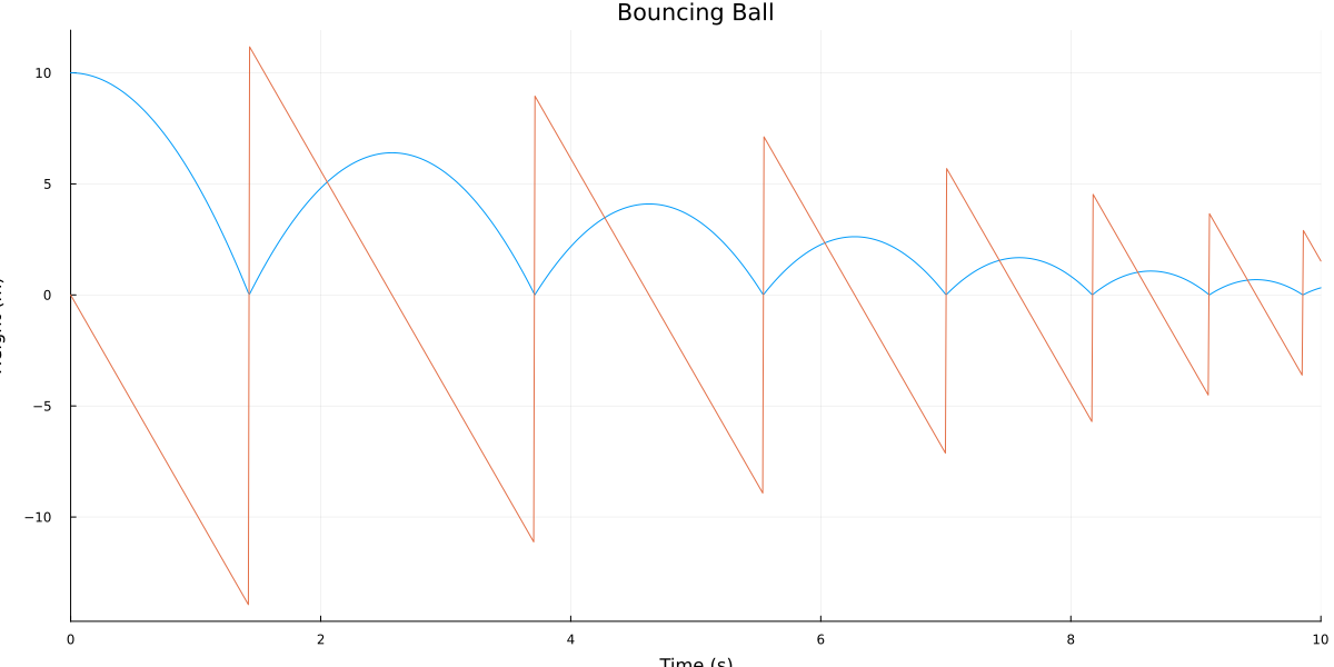
image-20260815154158538 \[ \begin{cases} \dot{x} = v \\ \dot{v} = -g \end{cases} \]

1
2
3
4
5
6
7
8
9
10
11
12
13
14
15
16
17
18
19
20
21
22
23
24
25
26
27
28
29
using DifferentialEquations
import Plots


function ball!(du, u, p, t)
g = 9.81

du[1] = u[2] # dx/dt = v
du[2] = -g # dv/dt = -g
end

function condition(u, t, integrator)
u[1] # event when x = 0
end

function bounce!(integrator)
e = 0.8
integrator.u[2] = -e * integrator.u[2]
end

cb = ContinuousCallback(condition, bounce!)

u0 = [10.0, 0.0]

prob = ODEProblem(ball!, u0, (0.0, 10.0))

sol = solve(prob, Tsit5(), callback=cb)

Plots.plot(sol, size=(1200, 600), title="Bouncing Ball", xlabel="Time (s)", ylabel="Height (m)", legend=false)

DiscreteCallback

The condition returns a Boolean

1
condition(u, t, integrator) = true/false

DiscreteCallback checks its Boolean condition at the end of accepted integration steps. It does not use root finding to locate the exact point where \(u=1\)
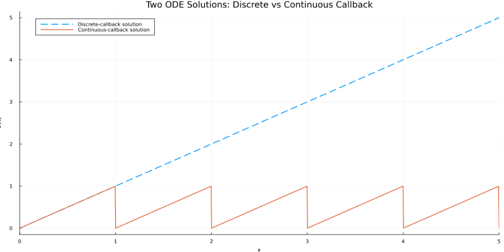
image-20260815161659197

1
2
3
4
5
6
7
8
9
10
11
12
13
14
15
16
17
18
19
20
21
22
23
24
25
26
27
28
29
30
31
32
33
34
35
36
37
38
39
40
41
42
43
44
45
46
47
48
49
using DifferentialEquations
import Plots

function f!(du, u, p, t)
du[1] = 1.0
end

u0 = [0.0]
tspan = (0.0, 5.0)

prob = ODEProblem(f!, u0, tspan)

# Boolean condition
function condition_DT(u, t, integrator)
u[1] >= 1.0
end

function condition_CT(u, t, integrator)
u[1] - 1.0
end

# Action when condition == true
function affect!(integrator)
integrator.u[1] = 0.0
end

cb_DT = DiscreteCallback(condition_DT, affect!)
cb_CT = ContinuousCallback(condition_CT, affect!)

sol_DT = solve(prob, Tsit5(), callback=cb_DT)
println("Discrete-callback solution time: ", sol_DT.t[end-1:end])
println("Discrete-callback solution: ", sol_DT.u[end-1:end])
# Discrete-callback solution time: [5.0, 5.0]
# Discrete-callback solution: [[4.999999999999999], [0.0]]

sol_CT = solve(prob, Tsit5(), callback=cb_CT)

plt = Plots.plot(
sol_DT,
title="Two ODE Solutions: Discrete vs Continuous Callback",
xlabel="Time",
ylabel="u(t)",
label="Discrete-callback solution",
linewidth=2,
linestyle=:dash,
legend=:topleft,
size=(1200, 600),
)
Plots.plot!(plt, sol_CT, label="Continuous-callback solution", linewidth=2)

DiscreteCallback checks only after each accepted solver step. Because du/dt = 1 is exactly linear, Tsit5() takes a large step from approximately t=0.58 directly to t=5. It therefore does not check near u=1.


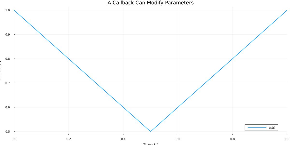
A callback can modify parameters

Callbacks provide the mechanism that connects the continuous ODE dynamics to this discrete switching behavior

So mathematically two components: \[ \dot{\mathbf{x}} = f(\mathbf{x}, p, t) \] for the \(\textbf{continuous-time dynamics}\), and \[ g(\mathbf{x}, t) = 0 \implies (\mathbf{x}, p) \to R(\mathbf{x}, p) \] for the \(\textbf{event/reset dynamics}\). \(R(x,p)\) means a reset map or event update rule

\[ \dot{x} = \begin{cases} -x, & x > 0.5 \\ -2x, & x < 0.5. \end{cases} \]

1
2
3
4
5
6
7
8
9
10
11
12
13
14
15
16
17
18
19
20
21
22
23
24
25
26
27
28
29
30
31
32
using DifferentialEquations
import Plots

function f!(du, u, p, t)
du[1] = -p[1]
end

function condition(u, t, integrator)
u[1] - 0.5
end

function affect!(integrator)
integrator.p[1] = -integrator.p[1]
end

p = [1.0]

cb = ContinuousCallback(condition, affect!)

prob = ODEProblem(f!, [1.0], (0.0, 1.0), p)

sol = solve(prob, Tsit5(), callback=cb)

Plots.plot(
sol,
title="A Callback Can Modify Parameters",
xlabel="Time (t)",
ylabel="State u₁(t)",
label="u₁(t)",
linewidth=2,
size=(1200, 600)
)

image-20260815164724091

reference

A. Demir, A. Mehrotra and J. Roychowdhury, "Phase noise in oscillators: a unifying theory and numerical methods for characterization," in IEEE Transactions on Circuits and Systems I: Fundamental Theory and Applications, vol. 47, no. 5, pp. 655-674, May 2000 [https://sci-hub.jp/10.1109/81.847872]

—, "A Reliable and Efficient Procedure for Oscillator PPV Computation, With Phase Noise Macromodeling Applications," IEEE TCAD, 2003.

— and A. Sangiovanni-Vincentelli, Analysis and Simulation of Noise in Nonlinear Electronic Circuits and Systems, vol. 425. Boston, MA, USA: Kluwer Academic Publishers, 1998

A. Mehrotra and A. Sangiovanni-Vincentelli, Noise Analysis of Radio Frequency Circuits, 1st ed. New York, NY, USA: Springer, 2004

Darabi H. Radio Frequency Integrated Circuits and Systems. 2nd ed. Cambridge University Press; 2020.


Mathematical Preliminaries

Strogatz, S.H. (2015). Nonlinear Dynamics and Chaos: With Applications to Physics, Biology, Chemistry, and Engineering (2nd ed.). CRC Press [https://www.biodyn.ro/course/literatura/Nonlinear_Dynamics_and_Chaos_2018_Steven_H._Strogatz.pdf]

Higham, Desmond. (2001). An Algorithmic Introduction to Numerical Simulation of Stochastic Differential Equations. SIAM Review. 43. 525-546. 10.1137/S0036144500378302. [https://www.cmor-faculty.rice.edu/~cox/stoch/dhigham.pdf]

Jiří Lebl. Notes on Diffy Qs: Differential Equations for Engineers [link]

Matt Charnley. Differential Equations: An Introduction for Engineers [link]

Åström, K.J. & Murray, Richard. (2021). Feedback Systems: An Introduction for Scientists and Engineers Second Edition [https://www.cds.caltech.edu/~murray/books/AM08/pdf/fbs-public_24Jul2020.pdf]
Decimation Filter

[https://web.engr.oregonstate.edu/~temes/ece627/Lecture_Notes/First_Order_DS_ADC_scan1.pdf]

[https://web.engr.oregonstate.edu/~temes/ece627/Lecture_Notes/First_Order_DS_ADC_scan2.pdf]

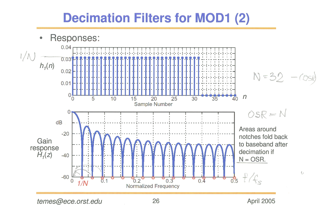
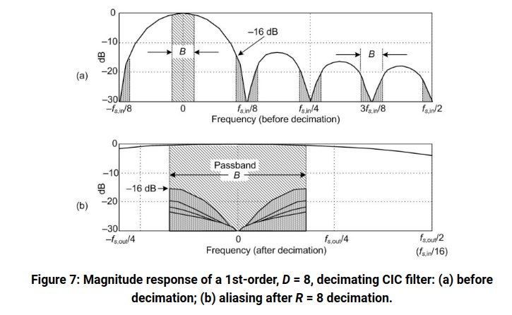
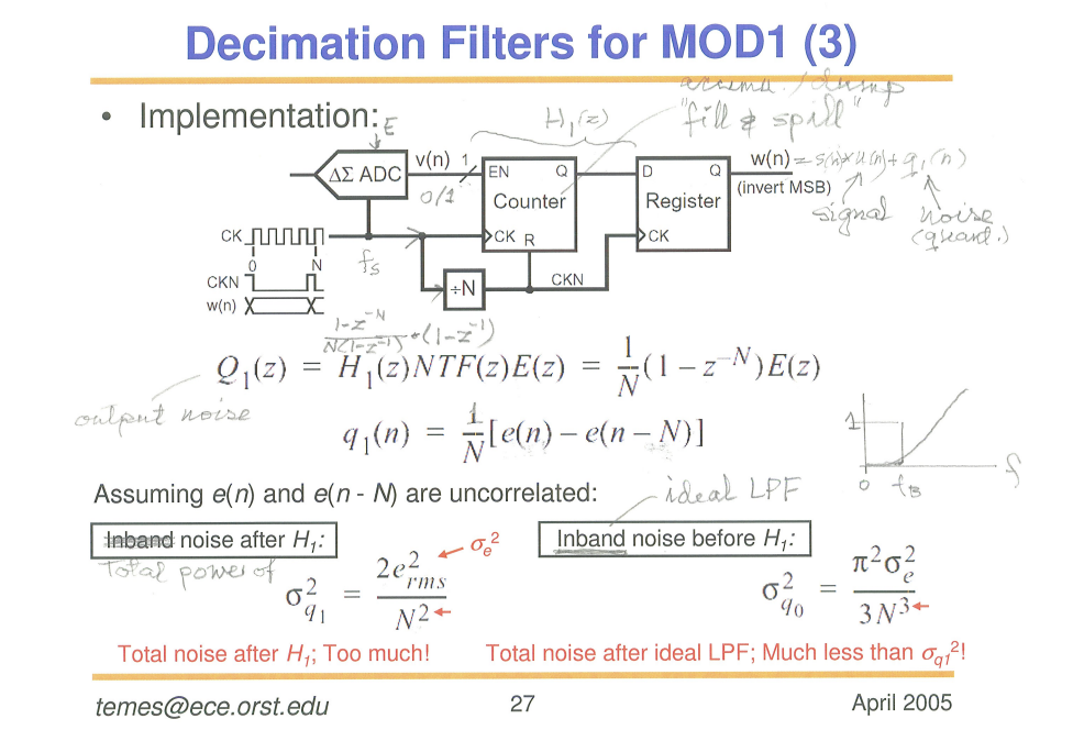
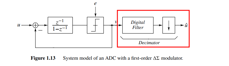
The combination of the the digital post-filter and downsampler is called the decimation filter or decimator

image-20241015220921002

\(\text{sinc}\) filter

image-20241015215159577

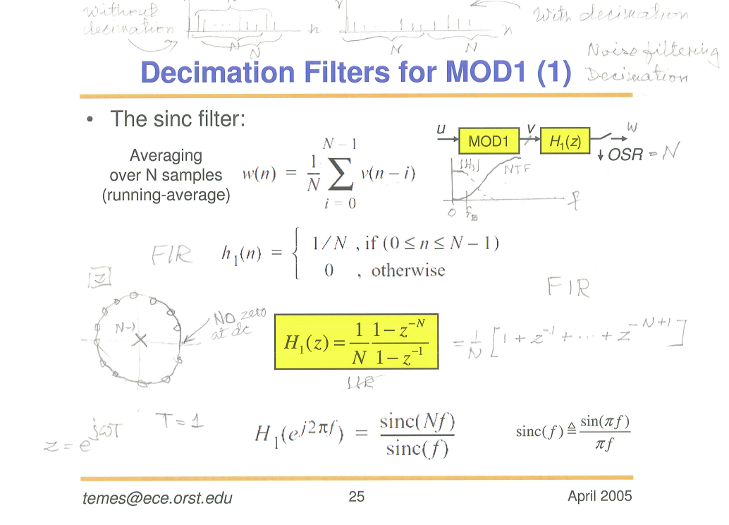
Suppose \(T=1\) \[ H_1(e^{j2\pi f}) = \frac{\text{sinc}(Nf)}{\text{sinc}(f)} = \frac{1}{N}\frac{\sin(\pi Nf)}{\sin(\pi f)} \] that is \(\lim_{f\to 0^+}H_1(e^{j2\pi f}) = 1\) and \(H_1 = 0\) when \(f=\frac{n}{N}, n\in \mathbb{Z}\)

image-20241015215227042

A Beginner's Guide To Cascaded Integrator-Comb (CIC) Filters [https://www.dsprelated.com/showarticle/1337.php]

image-20241015225859710

image-20241015215111430

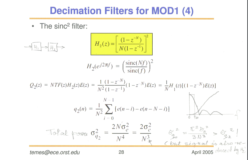
\[ |H_1(\omega)|^2 = \left|\frac{1}{N}(1-e^{-j\omega N}) \right| = \frac{2}{N^2}(1-\cos (\omega N)) \] Total noise after \(H_1\) \[ \sigma_{q_1}^2 = 2\int_0^\pi \frac{e^2_{rms}}{2\pi}\cdot |H_1(\omega)|^2d\omega = \frac{2e^2_{rms}}{N^2} \] inband noise before \(H_1\), i.e. ideal LPF with cutoff frequency \(\frac{\pi}{N}\) \[ \sigma_{q_0}^2 = 2\int_0^{\pi/N}\frac{e_{rms}^2}{2\pi}|1-e^{-j\omega}|^2d\omega = \frac{2e_{rms}^2}{\pi}\left(\frac{\pi}{N}-\sin\frac{\pi}{N}\right) \] with Taylor series \(\sin\frac{\pi}{N}\approx \frac{\pi}{N}-\frac{1}{6}\frac{\pi^3}{N^3}\) \[ \sigma_{q_0}^2 \approx \frac{\pi^2}{3N^3}e_{rms}^2 \]

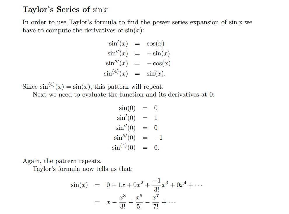
Taylor’s Series of \(\sin x\) [pdf]

image-20250913093652192


[https://analogicus.com/aic2025/2025/02/20/Lecture-6-Oversampling-and-Sigma-Delta-ADCs.html#python-oversample]

\(\text{sinc}^2\) filter

image-20241015220030204

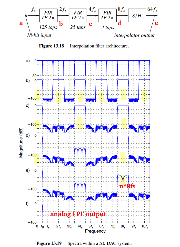
Interpolation Filter

Notice that the requirements of the first stage are very demanding

image-20250617001439043

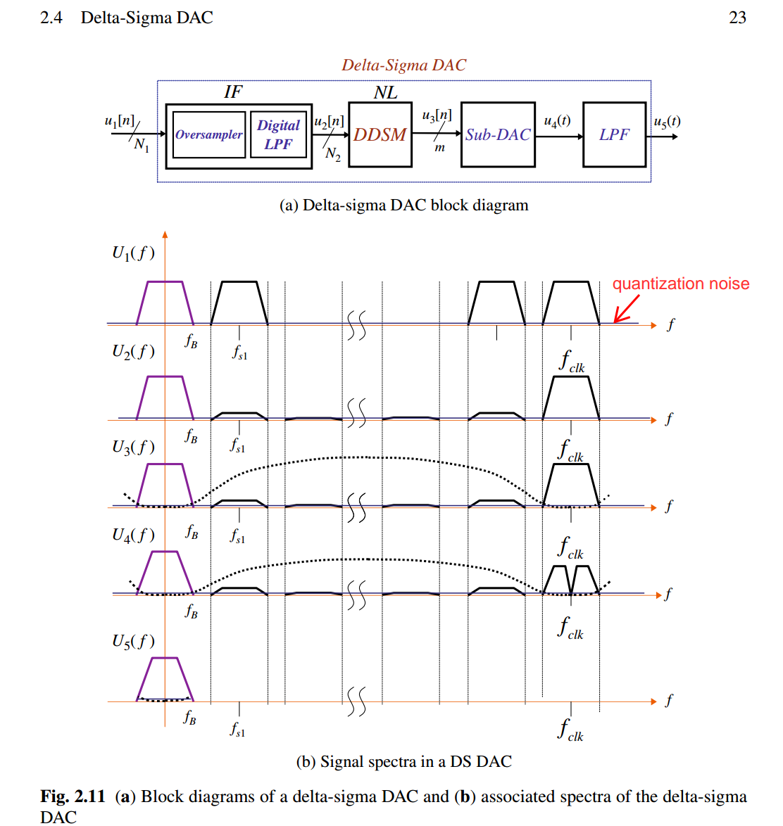
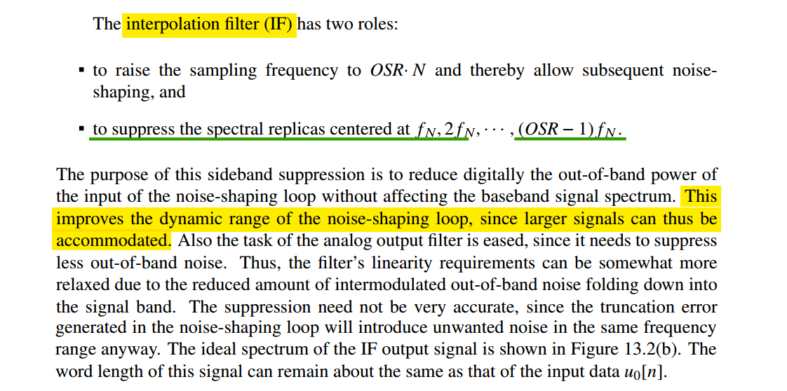
replicas suppression

The spectrum of the high resolution digital signal \(u_1\) contains the original baseband portion and its replicas located at integer multiples of \(f_{s1}\), plus a small amount of quantization noise shown as a solid line

image-20250906170436567

image-20250918220425431


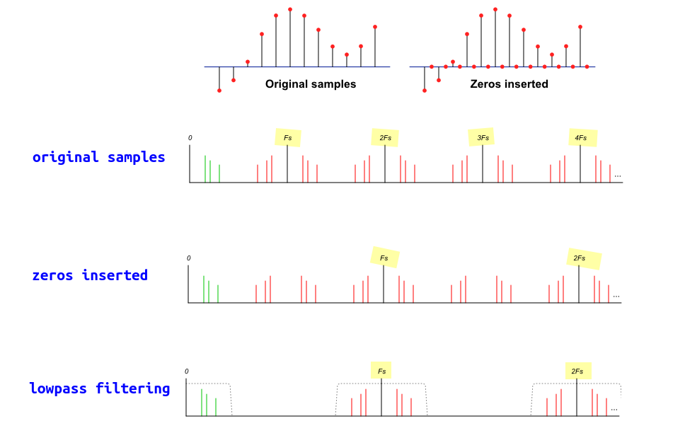
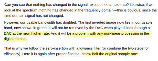
Nigel Redmon [https://dsp.stackexchange.com/a/63438/59253]

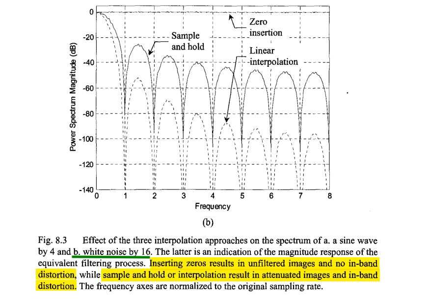
Inserting zeros changes nothing except what we consider the sample rate

image-20250920072501245

image-20250920074337023


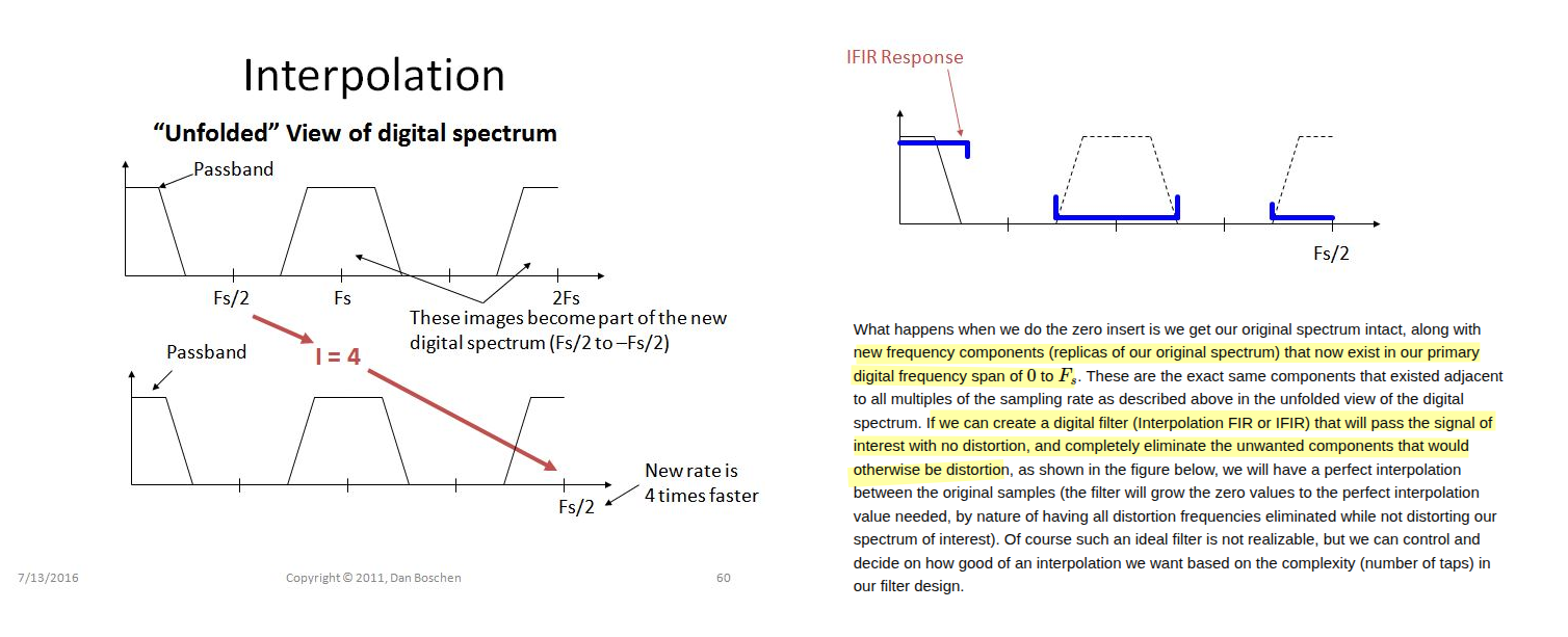
Dan Boschen [https://dsp.stackexchange.com/a/32130/59253]

image-20250920075212621


Bourdopoulos, G. I. (2003). Delta-Sigma modulators : modeling, design and applications. Imperial College Press. [pdf]

image-20250920080910057

DC Gain in IF

DC gain is used to compensate the ratio of sampling rate before and after upsample

image-20250701070539064

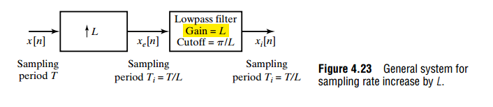
Given \[ X_e = X = \propto \frac{1}{T} = \frac{1}{L\cdot T_i} \] Then, the lowpass filter (ZOH, FOH .etc) gain shall be \(L\)


Employ definition of DTFT, \(X(e^{j\hat{\omega}}) =\sum_{n=-\infty}^{+\infty}x[n]e^{-j\hat{\omega} n}\), and set \(\hat{\omega} = 0\) \[ X(e^{j0}) = \sum_{n=-\infty}^{+\infty}x[n] \] That is, \(\sum_{n=-\infty}^{+\infty}x[n] = \sum_{n=-\infty}^{+\infty}x_e[n]\), so \[ \overline{x_e[n]} = \frac{1}{L} \overline{x[n]} \] It also indicate that dc gain of upsampling is \(1/L\)

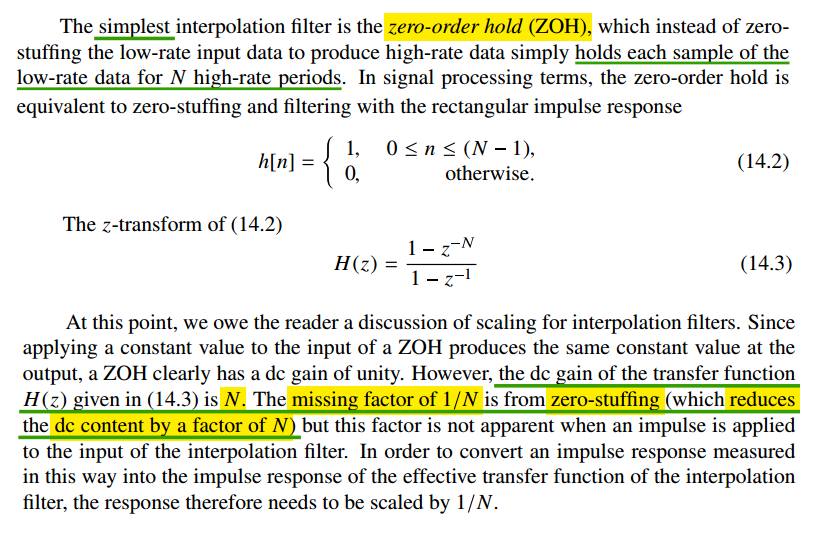
Zero-Order Hold (ZOH)

image-20250630235534325

dc gain = \(N\)

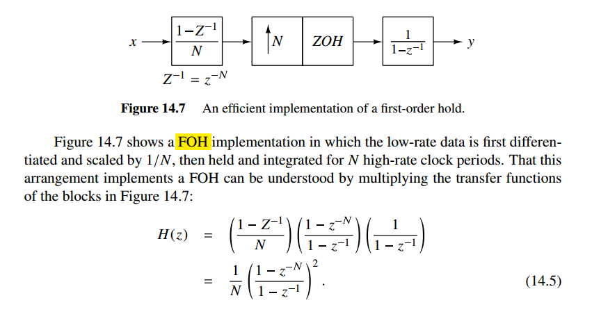
First-Order Hold (FOH)

image-20250630235714996

dc gain = \(N\)

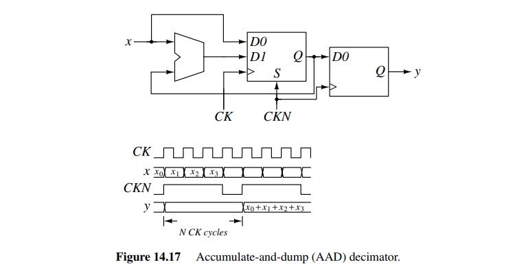
Accumulate-and-dump (AAD) decimator

accumulating the input for \(N\) cycles and then latching the result and resetting the integrator

image-20241015222205883

It adds up \(N\) succeeding input samples at rate \(1/T\) and delivers their sum in a single sample at the output. Therefore, the process comprises a filter (in the accumulation) and a down-sampler (in the dump)

Cascaded Integrator-Comb (CIC) filter

Qasim Chaudhari, Cascaded Integrator Comb (CIC) Filters – A Staircase of DSP [https://wirelesspi.com/cascaded-integrator-comb-cic-filters-a-staircase-of-dsp/]

Tom Verbeure. An Intuitive Look at Moving Average and CIC Filters [https://tomverbeure.github.io/2020/09/30/Moving-Average-and-CIC-Filters.html]

—. Half-Band Filters, a Workhorse of Decimation Filters [https://tomverbeure.github.io/2020/12/15/Half-Band-Filters-A-Workhorse-of-Decimation-Filters.html]

—. Design of a Multi-Stage PDM to PCM Decimation Pipeline [https://tomverbeure.github.io/2020/12/20/Design-of-a-Multi-Stage-PDM-to-PCM-Decimation-Pipeline.html]

Arash Loloee, Ph.D. Exploring Decimation Filters [https://www.highfrequencyelectronics.com/Archives/Nov13/1311_HFE_decimationFilters.pdf]

Let's focus on decimation: if we decimate by a factor 4, we simply retain one output sample out of every 4 input samples.

In the example below, the downsampler at the right drops those 3 samples out of 4, and the output rate, \(y^\prime(n)\), is one fourth of the input rate \(x(n)\):

moving_average_filters-decimation_trivial \[\begin{align} Y(z) &= X(z)\frac{1-z^{-4}}{1-z^{-1}} \\ Y^\prime(\xi) &= \frac{1}{4}Y(\xi^{1/4}) = \frac{1}{4}X(\xi^{1/4})\frac{1-\xi^{-1}}{1-\xi^{-1/4}} \end{align}\]

with \(z=e^{j\Omega/f_s}\) and \(\xi =z^4\), we have \[ Y^\prime(z) = \frac{1}{4}X(z)\frac{1-z^{-4}}{1-z^{-1}} \]

But if we're going to be throwing away 75% of the calculated values, can't we just move the downsampler from the end of the pipeline to somewhere in the middle? Right between the integrator stage and the comb stage? That answer is yes, but to keep the math working, we also need to divide the number of delay elements in the comb stage by the decimation rate:

moving_average_filters-decimation_smart

\[\begin{align} A(z) &= X(z)\frac{1}{1-z^{-1}} \\ A^\prime(\xi) &= \frac{1}{4}A(\xi^{1/4}) = \frac{1}{4}X(\xi^{1/4})\frac{1}{1-\xi^{-1/4}} \\ Y^\prime(\xi) &= A^\prime(\xi) (1-\xi^{-1}) = \frac{1}{4}X(\xi^{1/4})\frac{1-\xi^{-1}}{1-\xi^{-1/4}} \end{align}\]

with \(z=e^{j\Omega/f_s}\) and \(\xi =z^4\), we have \[ Y^\prime(z) = \frac{1}{4}X(z)\frac{1-z^{-4}}{1-z^{-1}} \]


And we can do this just the same with cascaded sections (without downsampler or updampler) where integrators and combs have been grouped

  • for decimation, the integrators come first and the combs second with the downsampler in between
  • For interpolation, the reverse is true
    • the incoming sample rate is fraction of the outgoing sample rate, the combs must come first and the interpolators second

moving_average_filters-integrator_comb_decimated

moving_average_filters-comb_integrator_interpolated

reference

Pavan, Shanthi, Richard Schreier, and Gabor Temes. (2016) 2016. Understanding Delta-Sigma Data Converters. 2nd ed. Wiley.

K. Hosseini and M. P. Kennedy, Minimizing Spurious Tones in Digital Delta-Sigma Modulators (Analog Circuits and Signal Processing). New York, NY, USA: Springer, 2011.


Neil Robertson, Model a Sigma-Delta DAC Plus RC Filter [https://www.dsprelated.com/showarticle/1642.php]

—, Modeling a Continuous-Time System with Matlab [https://www.dsprelated.com/showarticle/1055.php]

—, Modeling Anti-Alias Filters [https://www.dsprelated.com/showarticle/1418.php]

—, DAC Zero-Order Hold Models [https://www.dsprelated.com/showarticle/1627.php]

—, “A Simplified Matlab Function for Power Spectral Density”, DSPRelated.com, March, 2020, [https://www.dsprelated.com/showarticle/1333.php]

Ahmed Shahein (2026). MSD Toolbox (https://github.com/ahmedshahein/MSDTOOLBOX), GitHub. Retrieved April 25, 2026.

—, Multi-Decimation Stage Filtering for Sigma Delta ADCs: Design and Optimization [https://www.dsprelated.com/showarticle/1037.php]

Rick Lyons. A Beginner's Guide To Cascaded Integrator-Comb (CIC) Filters [https://www.dsprelated.com/showarticle/1337.php]

—, Optimizing the Half-band Filters in Multistage Decimation and Interpolation [https://www.dsprelated.com/showarticle/903.php]


Venkatesh Srinivasan, ISSCC 2019 T5: Noise Shaping in Data Converters

Nan Sun,IEEE CAS 2020: Break the kT/C Noise Limit [https://www.facebook.com/ieeecas/videos/break-the-ktc-noise-limit/322899188976197/]

Yun-Shiang Shu, ISSCC 2022 T3: Noise-Shaping SAR ADCs

Xiyuan Tang, CICC 2025 ES2-1: Noise-Shaping SAR ADCs - From Fundamentals to Recent Advances

image-20250612003115259


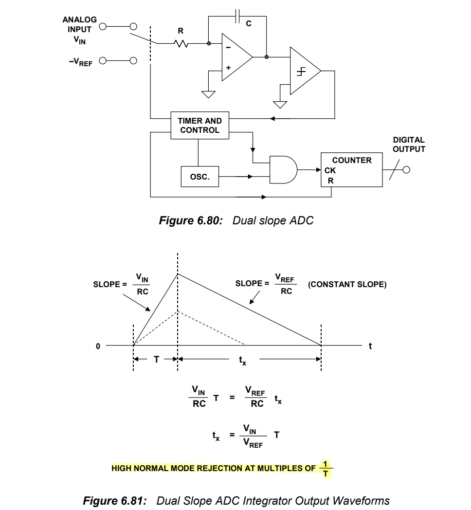
Dual Slope ADC

image-20250615153045770

image-20250615152228233

\[ V_{IN} = \frac{V_{REF}}{T}t_\text{x} = \frac{V_{REF}}{2^N}\cdot 2^{N_\text{x}} \]

Normal Mode Rejection

a high normal mode rejection ratio (NMRR) for input noise at line frequency

image-20250615160802268

  • Conversion accuracy is independent of both the capacitance and the clock frequency, because they affect both the up-slope and the down-slope by the same ratio

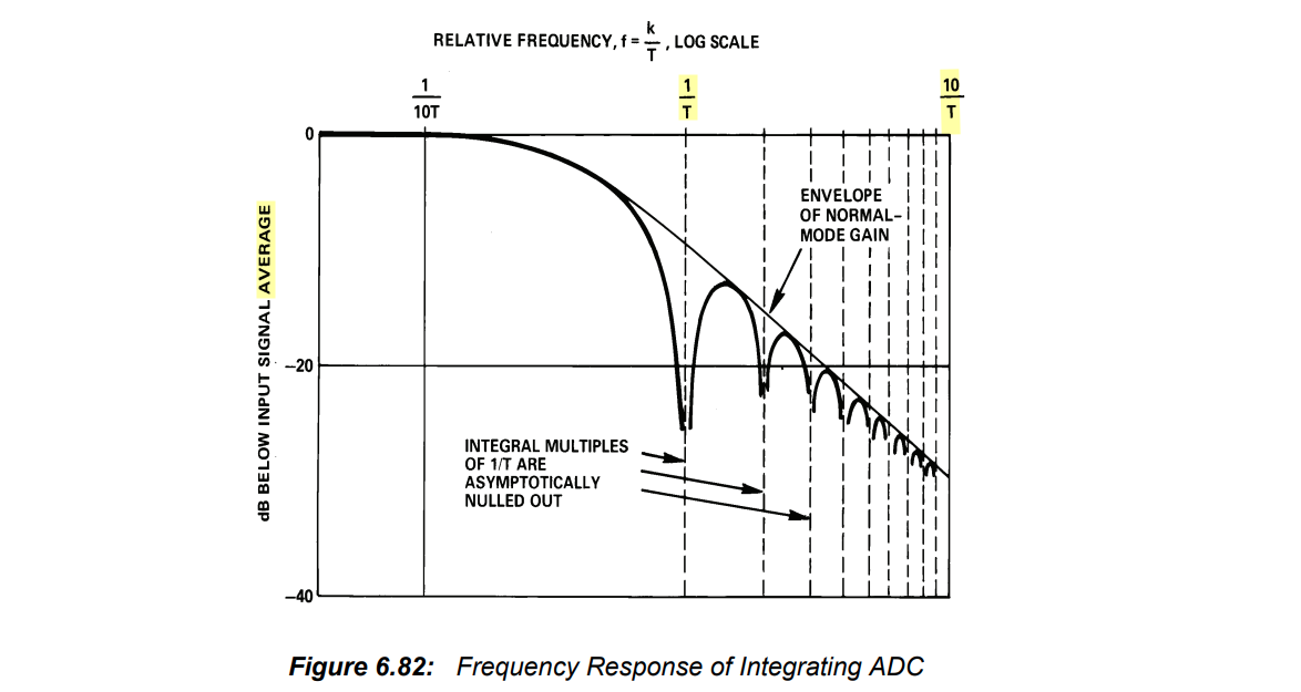
  • The fixed input signal integration period results in rejection of noise frequencies on the analog input that have periods that are equal to or a sub-multiple of the integration time \(T\)

    Interference signals with frequencies at integral multiples of the integration period are, theoretically, completely removed, since the average value of a sine wave of frequency (\(1/T\)) averaged over a period (\(T\)) is zero

image-20250615155921455

Linear Circuit Design Handbook, 2008 [https://www.analog.com/media/en/training-seminars/design-handbooks/Basic-Linear-Design/Chapter6.pdf]

Precision Analog Front Ends with Dual Slope ADC [https://ww1.microchip.com/downloads/aemDocuments/documents/APID/ProductDocuments/DataSheets/21428e.pdf]

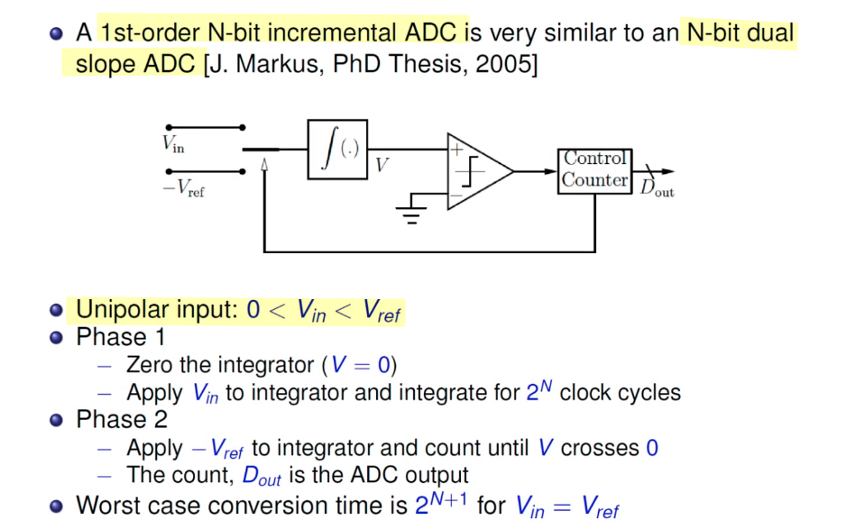
Incremental ADC

Z. Tan, C. -H. Chen, Y. Chae and G. C. Temes, "Incremental Delta-Sigma ADCs: A Tutorial Review," in IEEE Transactions on Circuits and Systems I: Regular Papers, vol. 67, no. 12, pp. 4161-4173, Dec. 2020 [https://sci-hub.jp/10.1109/TCSI.2020.3033458]

image-20250615124340044

image-20250615162024564

image-20250615162339449

image-20250615162358247

image-20250615170209562

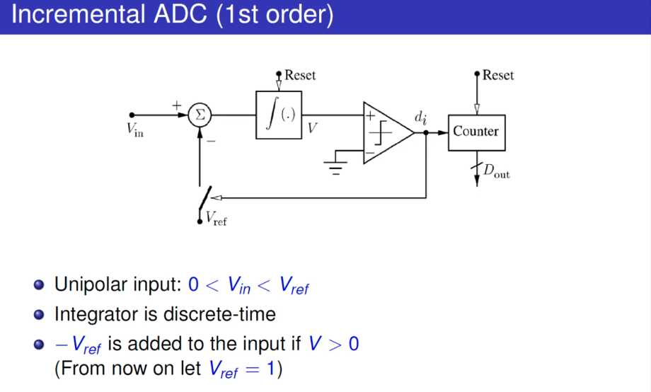
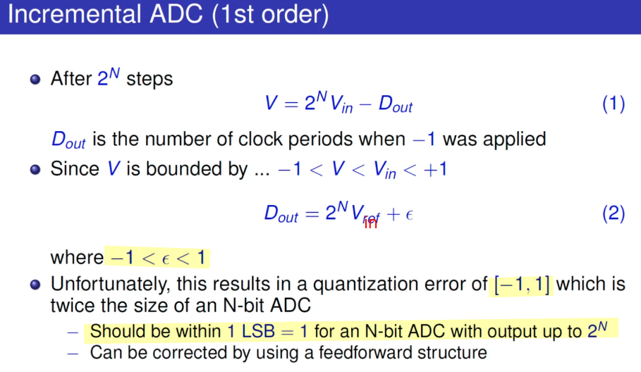
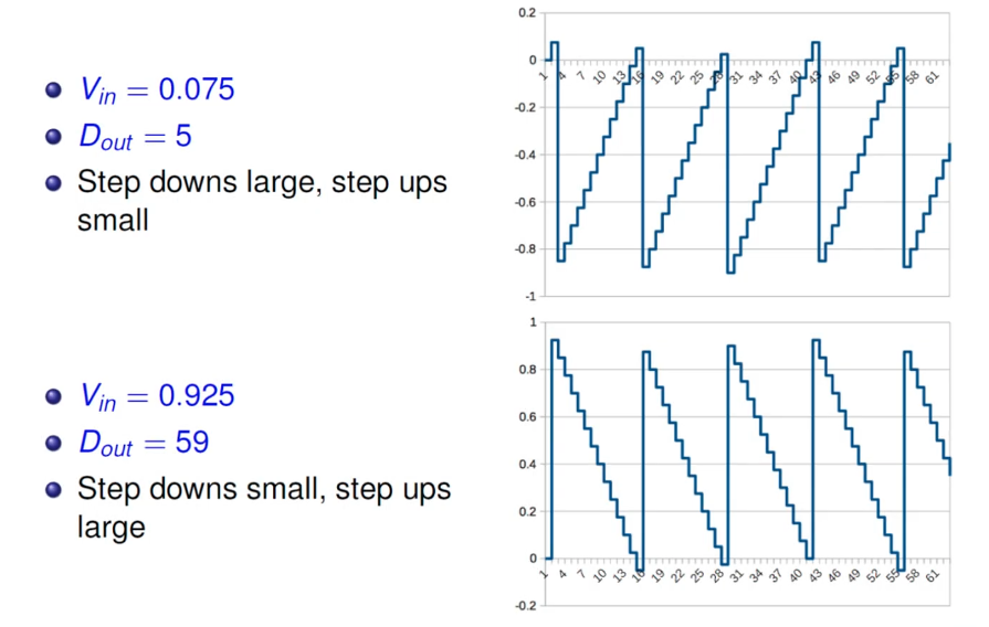
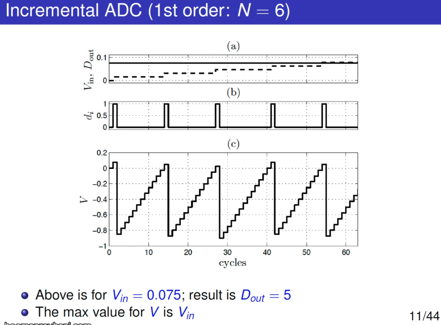
\[\begin{align} V &= 2^N V_\text{in} - D_\text{out}V_\text{ref} \\ D_\text{out} \frac{V_\text{ref}}{2^N} &= V_\text{in} - \frac{V}{2^N} \end{align}\]

image-20250615164436626

image-20250615192031025

feedforward structure

??? TODO 📅

image-20250615165107485

image-20250615175452958


image-20250615194549768

image-20250615194825368

image-20250615195150811

reference

David Johns (University of Toronto) "Oversampled Data Converters" Course (2019) [https://youtu.be/qIJ2LORYmyA]

Maurits Ortmanns , Paul Kaesser , Johannes Wagner (Dec 2025). Incremental Delta-Sigma ADCs Theory, Architectures and Design - Theory, Architectures and Design

image-20260914193314752

Frequency Domain Model

f-mdl.drawio

image-20260913094812184

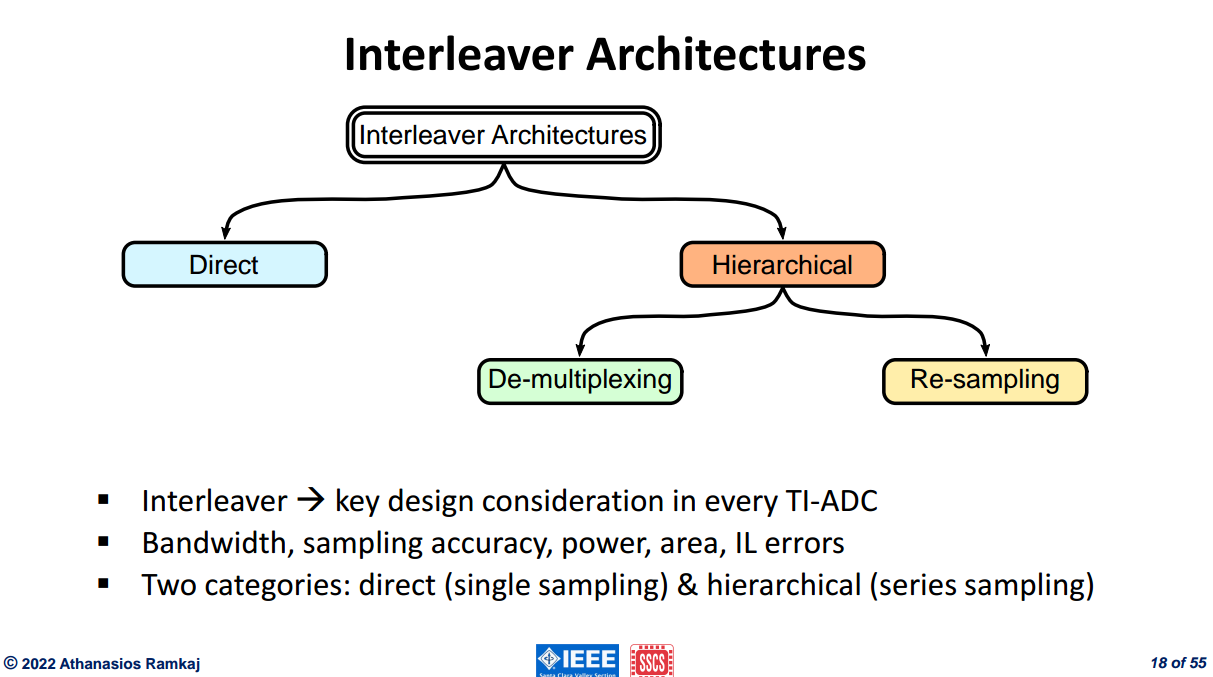
Interleaver Architectures

image-20260914194340521

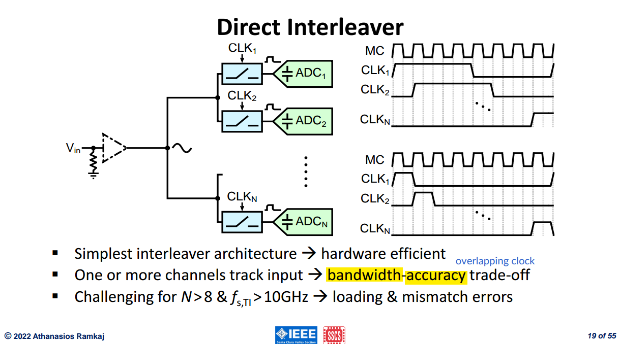
Direct Interleaver

image-20260914194944454

similar to increase the resolution of the flash ADC with more parallel comparators

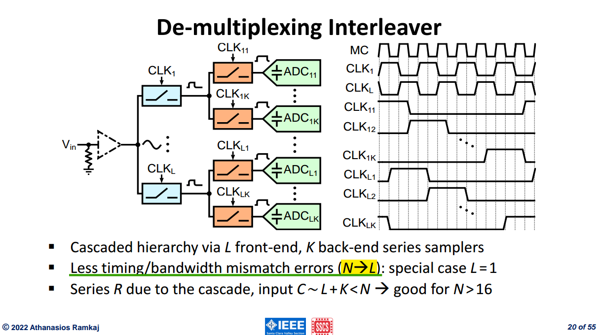
De-multiplexing Interleaver

image-20260914200548166

it is the front-end samplers that determine timing/bandwidth mismatch errors

only one front-end channel \(L=1\) eliminate any timing/bandwidth mismatch errors to the first order

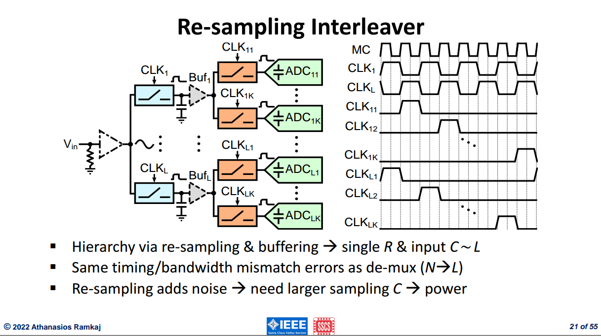
Re-sampling Interleaver

image-20260914195228805

back-end re-sampling occur after the front-end, two \(\frac{KT}{C}\) contribution in total noise (De-multiplexing Interleaver only one \(\frac{KT}{C}\))

without buffer, charging distribution reduce signal and reduce SNR, but buffers give excess noise


image-20260906160455591

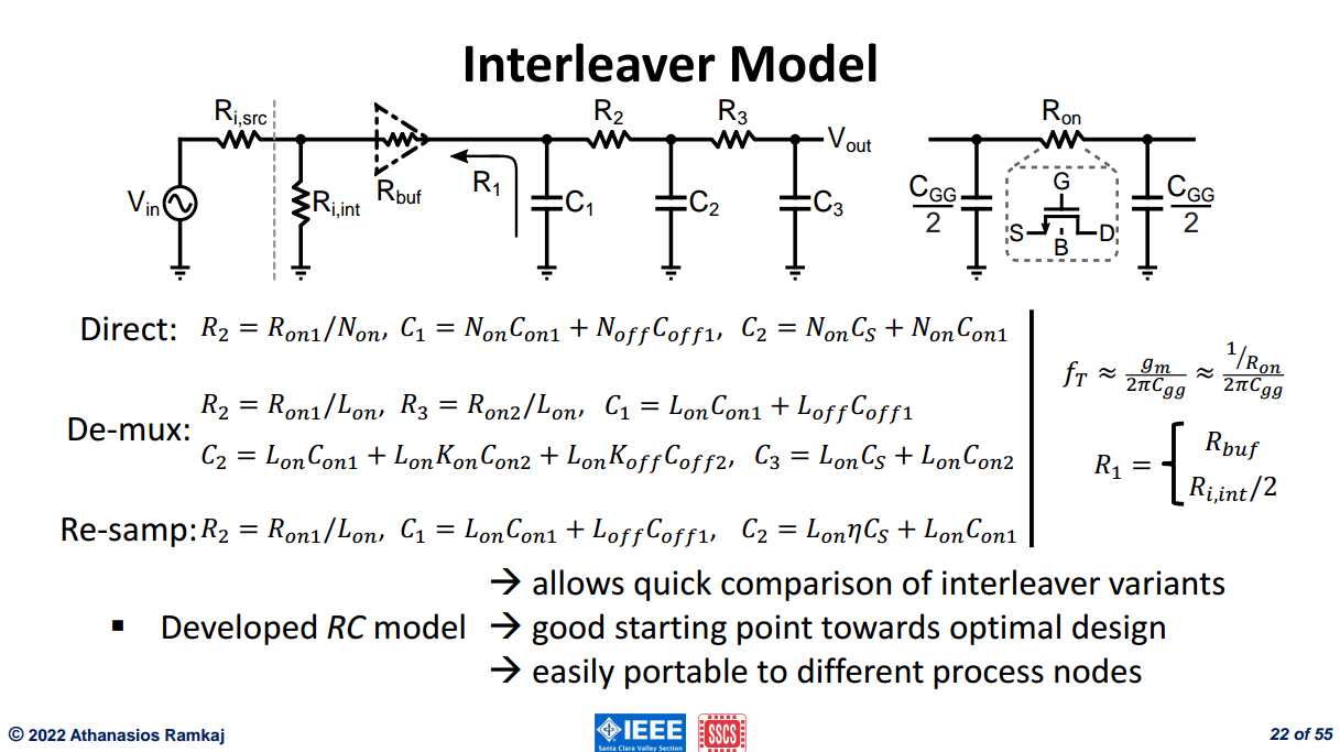
Interleaver Model

image-20260914195326519

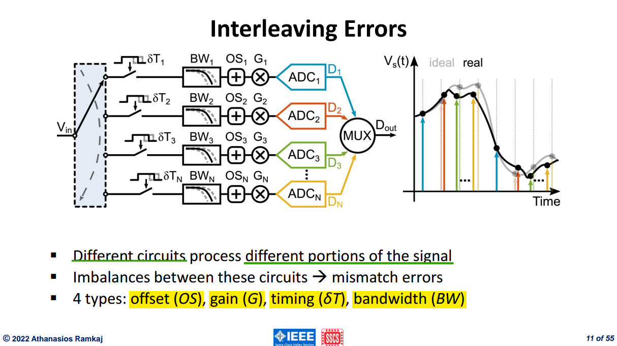
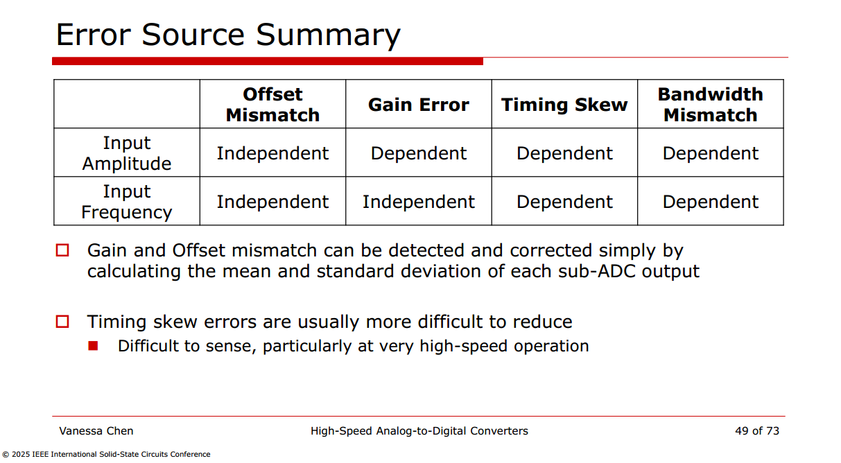
Interleaving Errors

image-20260914202358169

image-20260915213004819

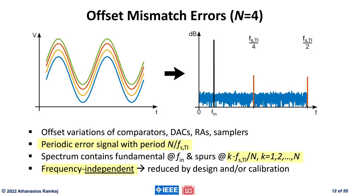
Offset Mismatch Errors

image-20260914202446007

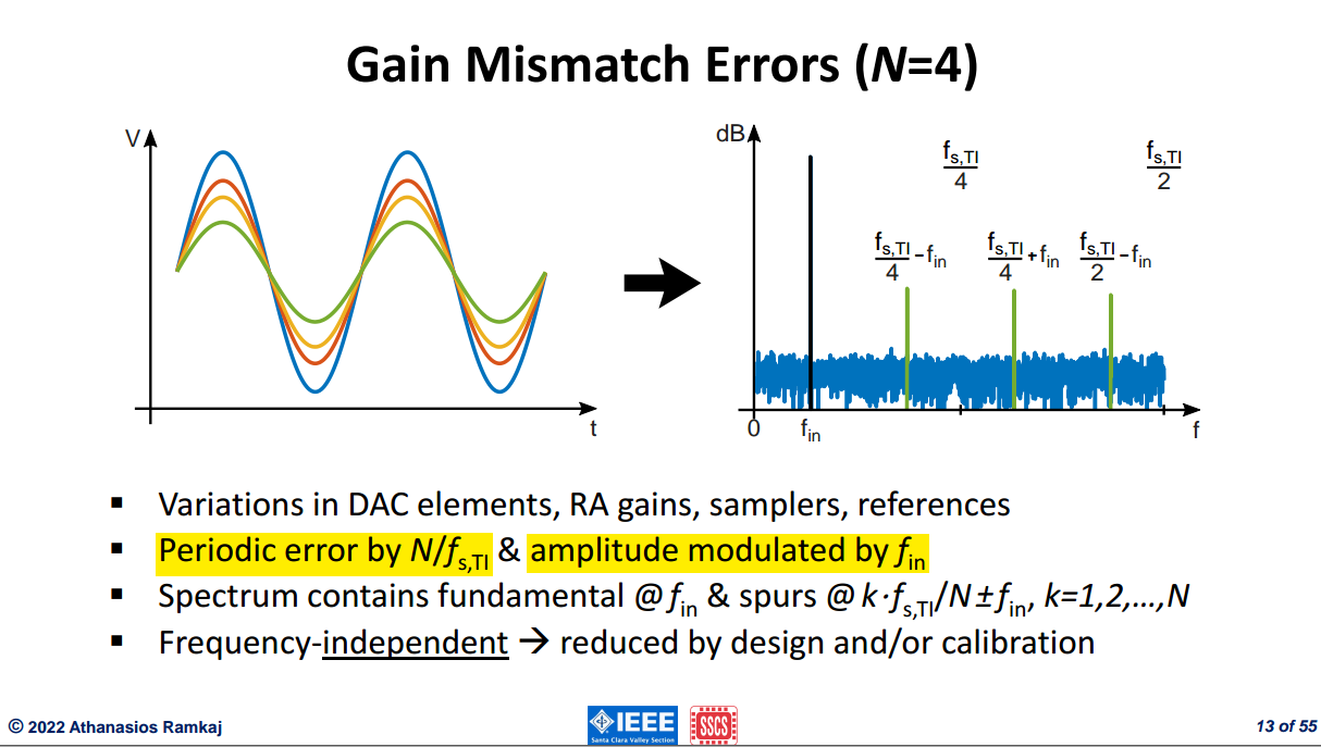
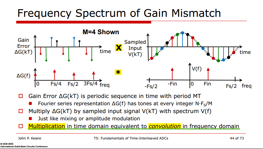
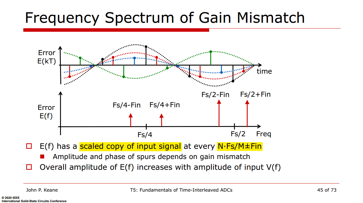
Gain Mismatch Errors

image-20260914202550362

image-20250621072944516

image-20260914210022880

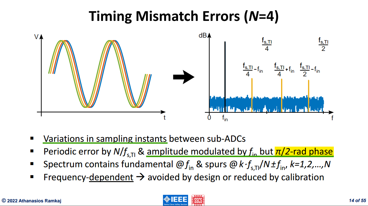
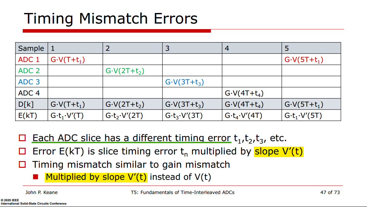
Timing Mismatch Errors

image-20260914204512858

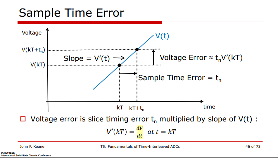
In the frequency domain,

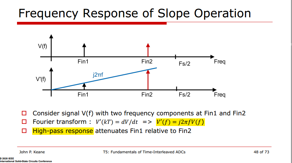
\[ \mathcal{L}\left\{ \frac{dV(t)}{dt} \right\} \;\longrightarrow\; sV(s) \quad\text{and, for }s=j\omega,\quad j\omega V(j\omega). \]

The factor

\[ j=e^{j\pi/2} \]

introduces a \(+\pi/2\) (90°) phase shift, while \(\omega\) scales the magnitude proportionally to frequency.

In the time domain,

\[ \frac{d}{dt}\sin(\omega t) =\omega\cos(\omega t) =\omega\sin\left(\omega t+\frac{\pi}{2}\right). \]

Thus, differentiation produces two effects: magnitude scaling by \(\omega\) and a \(90^\circ\) phase advance.

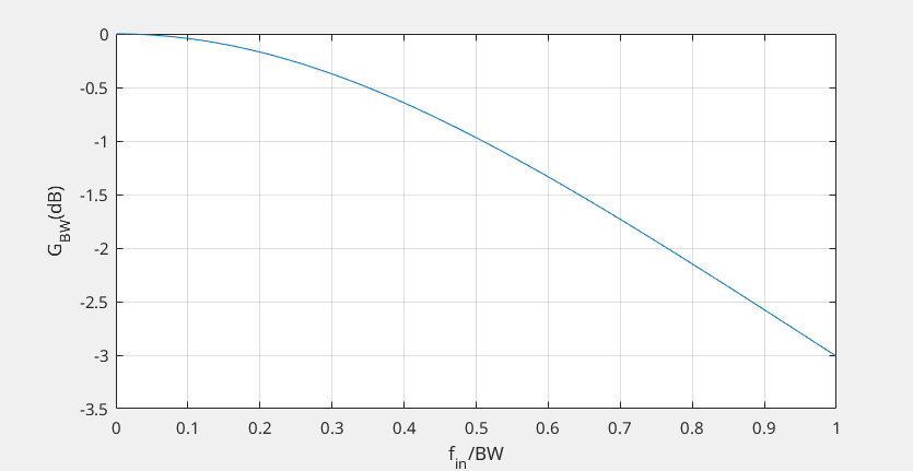
Frequency-dependent: the higher frequency input signal \(f_\text{in}\), the larger error becomes

image-20250621091024424

image-20260914210257078

image-20250621091047339

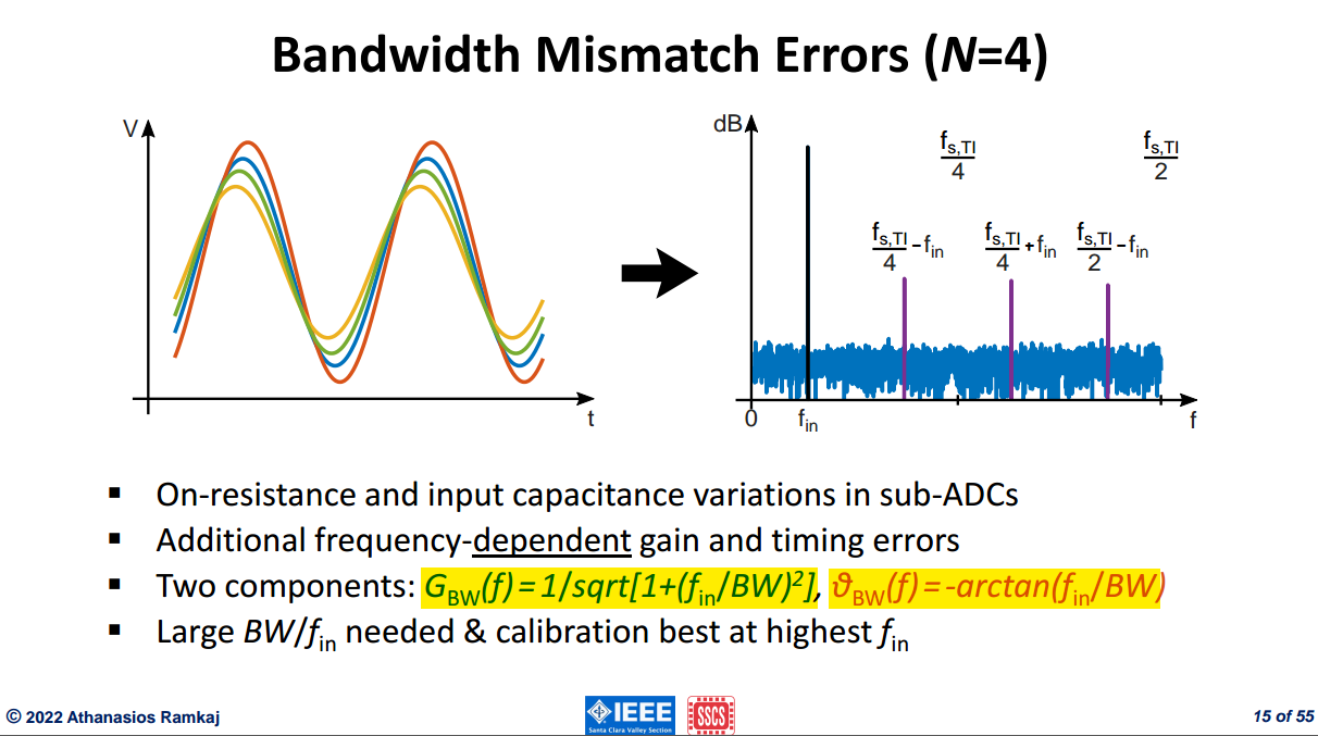
Bandwidth Mismatch Errors

image-20260914202752033

image-20250621093321623

resync (alignment)

TODO 📅

Calibration Techniques

image-20260324180833001

Autocorrelation-based Skew Calibration

S. Chen, L. Wang, H. Zhang, R. Murugesu, D. Dunwell, A. Chan Carusone, “All-Digital Calibration of Timing Mismatch Error in Time-Interleaved Analog-to-Digital Converters,” IEEE Transactions on VLSI Systems, Sept. 2017. [PDF, slides]

B. Razavi, "Problem of timing mismatch in interleaved ADCs," Proceedings of the IEEE 2012 Custom Integrated Circuits Conference, San Jose, CA, USA, 2012 [pdf]

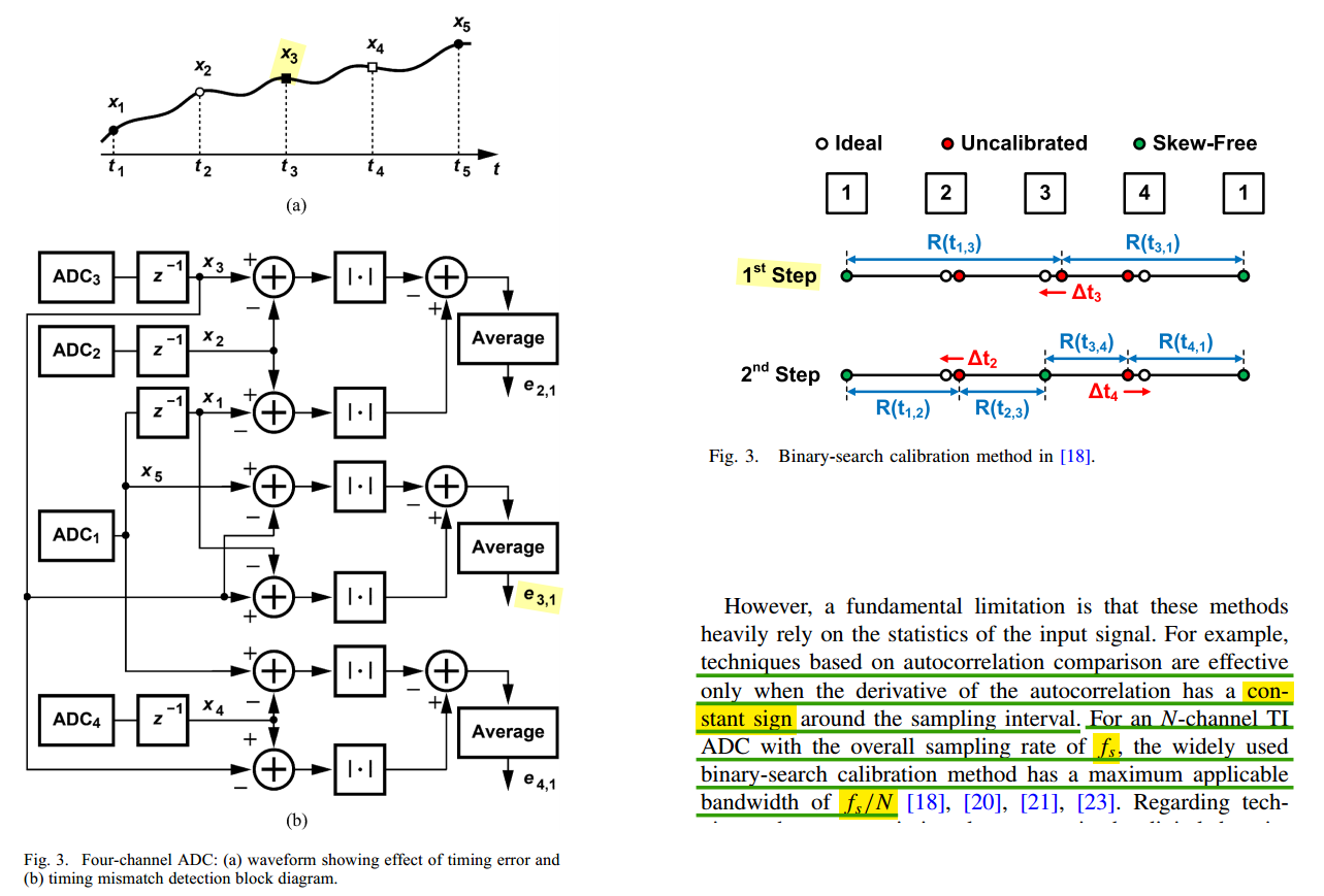
Binary-Search Calibration Method & its limitations

image-20260328225656118


M. Gu, Y. Tao, X. He, Y. Zhong, L. Jie and N. Sun, "A 1-GS/s 11-b Time-Interleaved SAR ADC With Robust, Fast, and Accurate Autocorrelation-Based Background Timing-Skew Calibration," in IEEE Journal of Solid-State Circuits, vol. 60, no. 2, pp. 421-431, Feb. 2025

—. "Timing-Skew Calibration Techniques in Time-Interleaved ADCs," in IEEE Open Journal of the Solid-State Circuits Society, vol. 5, pp. 1-10, 2025 [https://ieeexplore.ieee.org/stamp/stamp.jsp?tp=&arnumber=10804623]

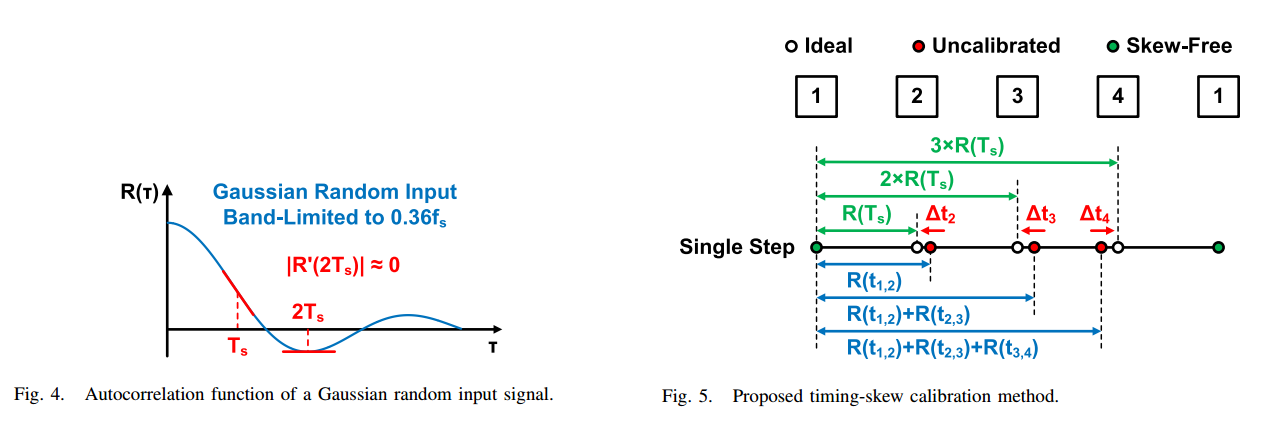
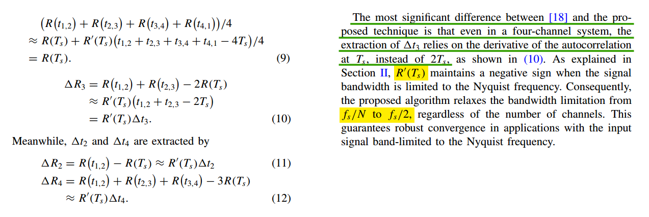
An autocorrelation-based background timing-skew calibration method, which uses the correlations between adjacent channels to extract timing-skew errors, which relaxes the input bandwidth limitation up to the Nyquist frequency

image-20260330204902627

image-20260330205119231


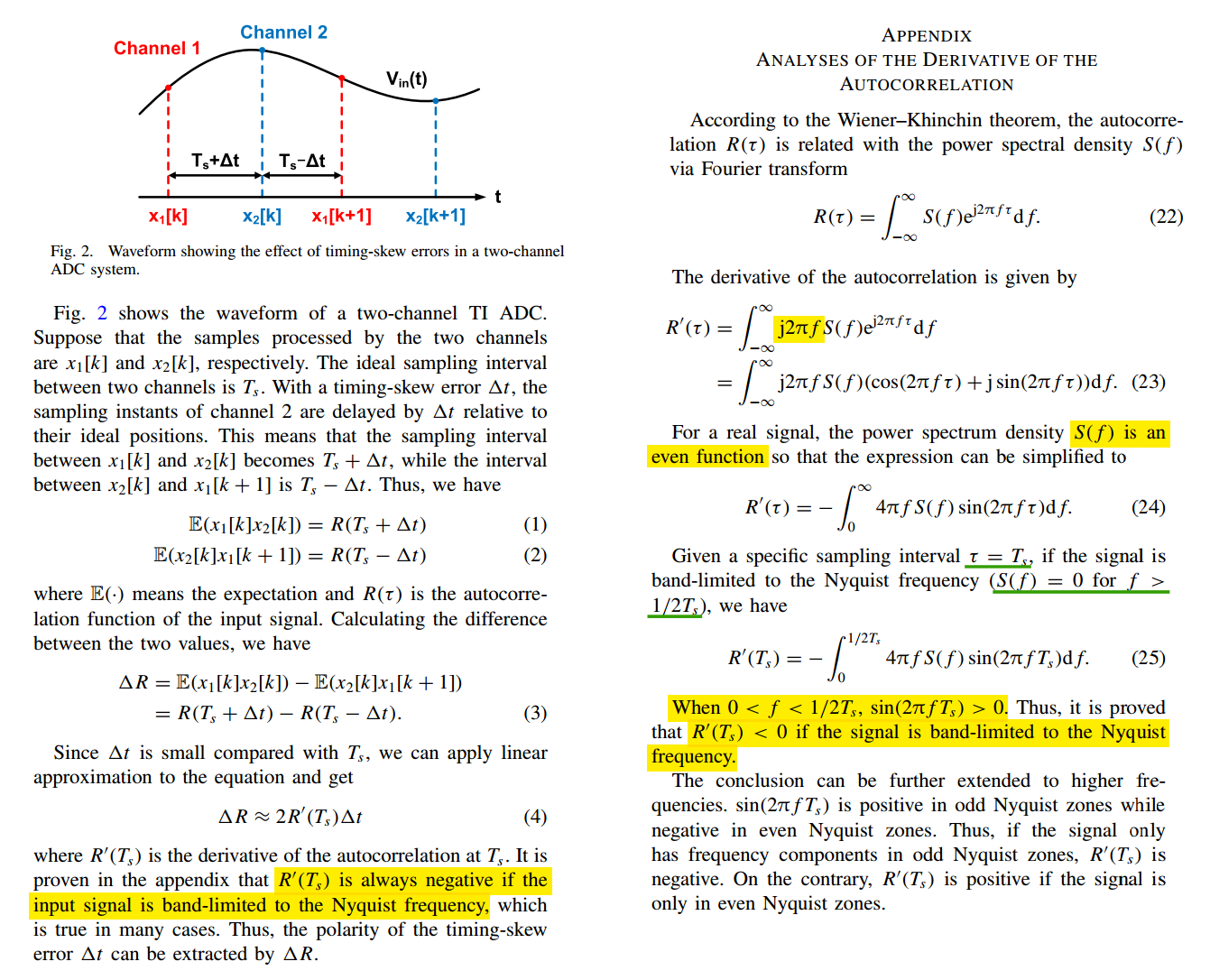
Analyses Of The Derivative of The Autocorrelation

image-20260324183003185

MAD (Mean Absolute Difference) vs. correlation

H. Wei, P. Zhang, B. Datta Sahoo and B. Razavi, "An 8-Bit 4-GS/s 120-mW CMOS ADC," Proceedings of the IEEE 2013 Custom Integrated Circuits Conference, San Jose, CA, USA, 2013 [pdf]

—, "An 8 Bit 4 GS/s 120 mW CMOS ADC," in IEEE Journal of Solid-State Circuits, vol. 49, no. 8, pp. 1751-1761, Aug. 2014 [pdf]

M. Gu, Y. Tao, X. He, Y. Zhong, L. Jie and N. Sun, "A 1-GS/s 11-b Time-Interleaved SAR ADC With Robust, Fast, and Accurate Autocorrelation-Based Background Timing-Skew Calibration," in IEEE Journal of Solid-State Circuits, vol. 60, no. 2, pp. 421-431, Feb. 2025

TODO 📅

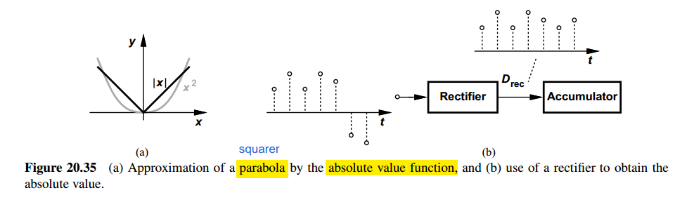
approximate the absolute value operation by a squaring function

image-20260328212413965

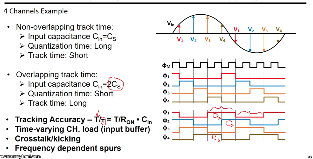
Overlapping versus Non-overlapping track time

image-20250611224418950

tracking accuracy stay same, Cin (2Cs) counteract the longer tracking

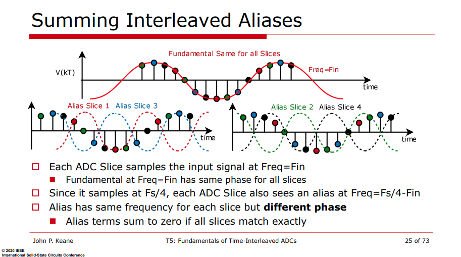
Summing Interleaved Alias

image-20240929215841300

The sampling function - impulse train is \[ s(t) = \sum_{n=-\infty}^{\infty}\left[ \delta(t-n4T_s) + \delta(t-n4T_s-T_s) + \delta(t-n4T_s-2T_s) + \delta(t-n4T_s-3T_s)\right] \]

Its Fourier transform is \[\begin{align} S(f) &= \frac{2\pi}{4T}\sum_{k=-\infty}^{\infty}\left[\delta(f-k\frac{f_s}{4}) + e^{-j2\pi f\cdot T_s}\delta(f-k\frac{f_s}{4}) + e^{-j2\pi f\cdot 2T_s}\delta(f-k\frac{f_s}{4}) + e^{-j2\pi f\cdot 3T_s}\delta(f-k\frac{f_s}{4}) \right] \\ &= \frac{2\pi}{4T}\sum_{k=-\infty}^{\infty}\left(1+e^{-j2\pi\frac{f}{f_s}} + e^{-j4\pi\frac{f}{f_s}} + e^{-j6\pi\frac{f}{f_s}} \right) \delta(f-k\frac{f_s}{4}) \\ &= \frac{2\pi}{4T}\sum_{k=-\infty}^{\infty}\left(1+e^{-jk\frac{\pi}{2}} + e^{-jk\pi} + e^{-jk\frac{3\pi}{2}} \right) \delta(f-k\frac{f_s}{4}) \end{align}\]

We define \(M[k] = 1+e^{-jk\frac{\pi}{2}} + e^{-jk\pi} + e^{-jk\frac{3\pi}{2}}\), which is periodic, i.e. \(M[k]=M[k+4]\) \[ M[k]=\left\{ \begin{array}{cl} 4 & : \ k = 4m \\ 0 & : \ k=4m+1 \\ 0 & : \ k=4m+2 \\ 0 & : \ k=4m+3 \\ \end{array} \right. \]

That is \[ S(f) = \frac{2\pi}{T}\sum_{k=-\infty}^{\infty} \delta(f-kf_s) \]

Alias has same frequency for each slice but different phase: Alias terms sum to zero if all slices match exactly

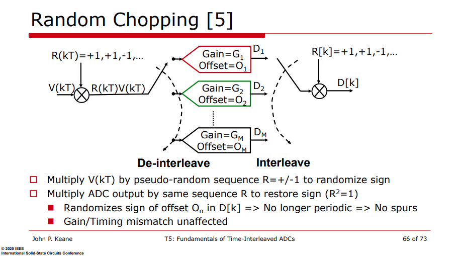
Random Chopping in TI-ADC

image-20240929215927957

\[ D_n(kT) = (G_n R(kT) V(kT) + O_n)R(kT)= C_n V(kT) + R(kT)O_n \]

ADC buffers & memory effect

Y. Shifman, Y. Krupnik, U. Virobnik, A. Khairi, Y. Sanhedrai and A. Cohen, "A 1.64mW Differential Super Source-Follower Buffer with 9.7GHz BW and 43dB PSRR for Time-Interleaved ADC Applications in 10nm," 2019 IEEE Asian Solid-State Circuits Conference (A-SSCC), Macau, Macao, 2019 [pdf]

E. -H. Chen et al., "7.1 A 212.5Gb/s DSP-Based PAM-4 Transceiver with 50dB Loss Compensation for Large AI System Interconnects in 4nm FinFET," 2025 IEEE International Solid-State Circuits Conference (ISSCC), San Francisco, CA, USA, 2025

TODO 📅

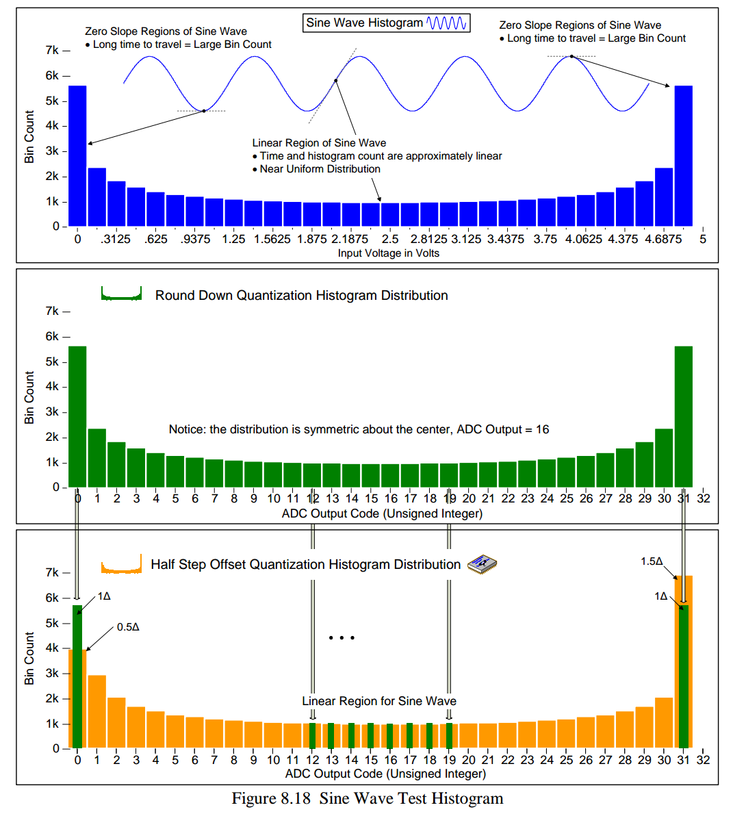
DNL/INL Benefit

Each sub-ADC has its own physical capacitor array, so each slice has its own independent, zero-mean mismatch error

Because the sub-ADC are sampled round-robin, a busy input signal visits all \(N\) sub-ADC with equal probability over the whole input range. The transfer curve that the composite output presents is therefore the ensemble average \[ e_{\mathrm{eff}}(k) = \frac{1}{N}\sum_{i=1}^{N} e_i(k) \quad\Rightarrow\quad \sigma\!\left\{e_{\mathrm{eff}}(k)\right\} = \frac{\sigma\{e_i(k)\}}{\textcolor{red}{\sqrt{N}}} \] the measured static DNL/INL genuinely improves by \(\sqrt{N}\) at code-density (histogram) test

The composite result \[ \boxed{\sigma_{DNL,\max}^{TI} = \frac{\sigma_{\text{sub},DNL}}{\sqrt{N}}, \qquad \sigma_{INL,\max}^{TI} = \frac{\sigma_{\text{sub},INL}}{\sqrt{N}}} \] where \(N\) is channel number

Conventional binary array sub-SARADC \[ \sigma_{DNL,\max}=\sqrt{2^n-1}\,\frac{\sigma_u}{C_u}\,[\mathrm{LSB}], \qquad \sigma_{INL,\max}=\frac{\sqrt{2^n}}{2}\,\frac{\sigma_u}{C_u}\,[\mathrm{LSB}] \] VCM-based (\(n-1\) bit array) sub-SARADC

In a VCM-based (top-plate-sampled, tri-level) SAR, the MSB decision needs no capacitor switching at all — it's a direct comparison against \(V_{CM}\) \[ \sigma^{VCM}_{DNL,\max} = \sqrt{2^{n-1}-1}\,\frac{\sigma_u}{C_u}, \qquad \sigma^{VCM}_{INL,\max} = \frac{\sqrt{2^{n-1}}}{2}\,\frac{\sigma_u}{C_u} \qquad \text{at } k=2^{n-2},\,3\cdot 2^{n-2} \]


image-20260913173227688

Paper from industry

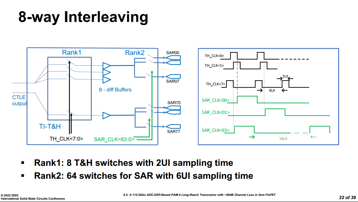
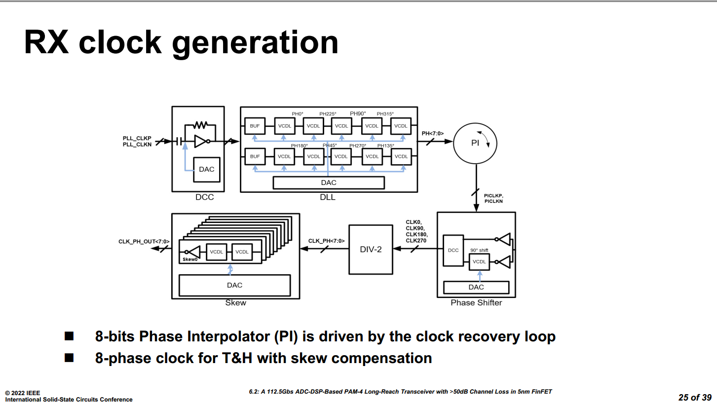
Z. Guo et al., "A 112.5Gb/s ADC-DSP-Based PAM-4 Long-Reach Transceiver with >50dB Channel Loss in 5nm FinFET," 2022 IEEE International Solid-State Circuits Conference (ISSCC), San Francisco, CA, USA, 2022 [https://sci-hub.st/10.1109/ISSCC42614.2022.9731650]

image-20250806224145281

8way-interleaving-Marvell-ISSCC2022.drawio


P. Liu et al., "A 128Gb/s ADC/DAC Based PAM-4 Transceiver with >45dB Reach in 3nm FinFET," 2025 Symposium on VLSI Technology and Circuits (VLSI Technology and Circuits), Kyoto, Japan, 2025

image-20250808220954208

image-20250808221134749

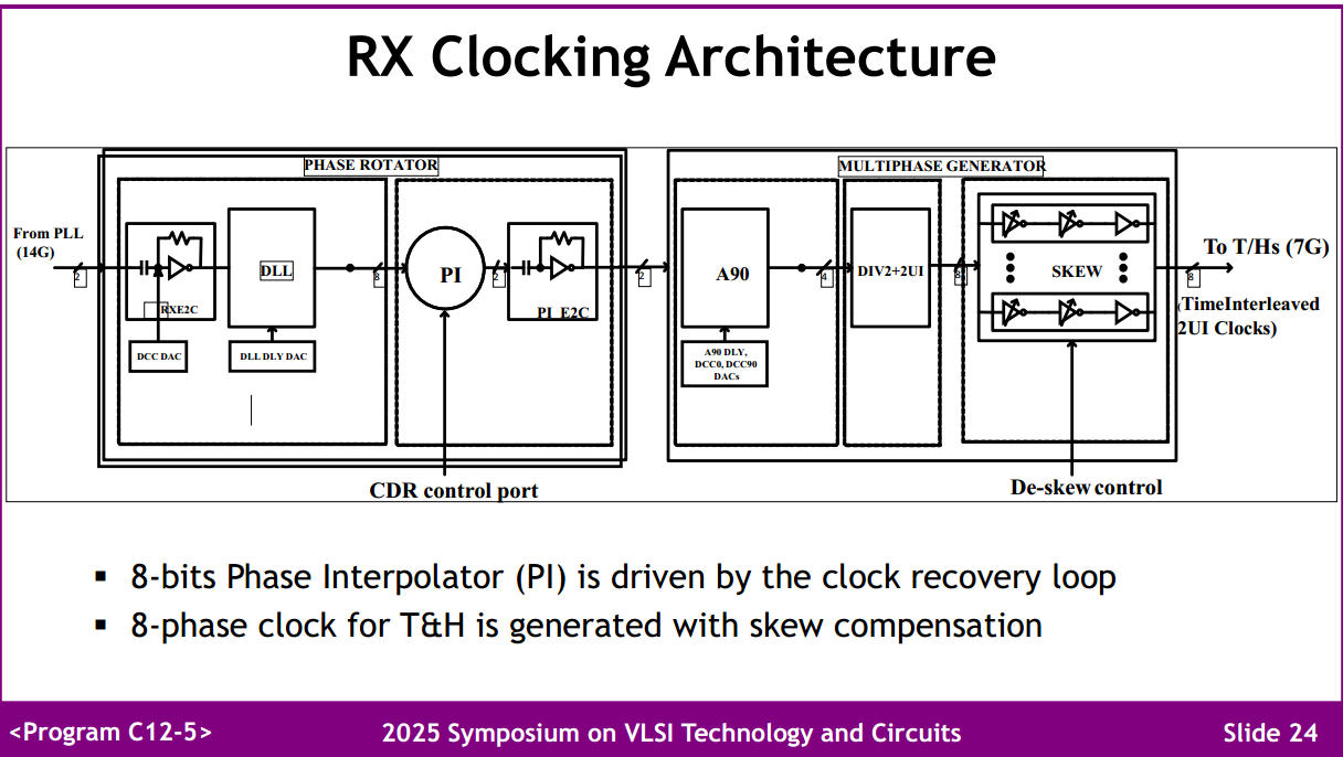
RX-Clocking-Marvell-VLSI2025.drawio


ISSCC.2024 7.3 A 224Gbs 3pJb 40dB Insertion Loss Transceiver in 3nm FinFET CMOS [7.3 A 224Gbs 3pJb 40dB Insertion Loss Transceiver in 3nm FinFET CMOS https://www.bilibili.com/video/BV18hYCe7E45/?share_source=copy_web&vd_source=5a095c2d604a5d4392ea78fa2bbc7249]

ISSCC.2018 6.4 A Fully Adaptive 19-to-56Gb/s PAM-4 Wireline Transceiver with a Configurable ADC in 16nm FinFET [https://sci-hub.st/10.1109/ISSCC.2018.8310207]

M. S. Jalali, A. Sheikholeslami, M. Kibune and H. Tamura, "A Reference-Less Single-Loop Half-Rate Binary CDR," in IEEE Journal of Solid-State Circuits, vol. 50, no. 9, pp. 2037-2047, Sept. 2015 [https://www.eecg.utoronto.ca/~ali/papers/jssc2015-09.pdf]

Pisati, et.al., "Sub-250mW 1-to-56Gb/s Continuous-Range PAM-4 42.5dB IL ADC/DAC- Based Transceiver in 7nm FinFET," 2019 IEEE International Solid-State Circuits Conference (ISSCC), 2019 [https://sci-hub.se/10.1109/ISSCC.2019.8662428]

reference

Poulton, Ken. ISSCC2009 "Time-Interleaved ADCs, Past and Future" (slides)

—. CICC2010 "GHz ADCs: From Exotic to Mainstream", tutorial session, (slides)

—. ISSCC2015 "Interleaved ADCs Through the Ages", (slides)

ISSCC2015 F1: High-Speed Interleaved ADCs

Samuel Palermo, ISSCC 2018 T10: ADC-Based Serial Links: Design and Analysis

Ewout Martens. ESSCIRC 2019 Tutorials: Advanced Techniques for ADCs for 5G Massive MIMO [https://youtu.be/7hYichGGU6k]

Yohan Frans, CICC2019 ES3-3- "ADC-based Wireline Transceivers" [pdf]

John P. Keane, ISSCC2020 T5: "Fundamentals of Time-Interleaved ADCs"

Athanasios Ramkaj. January 26, 2022, IEEE SSCS Santa Clara Valley Section Technical Talk: Design Considerations Towards Optimal High-Resolution Wide-Bandwidth Time-Interleaved ADCs [video] [slides]

V. Chen, "Tutorial: High-Speed Analog-to-Digital Converters," 2025 IEEE International Solid-State Circuits Conference (ISSCC), San Francisco, CA, USA, 2025, pp. 1-1, doi: 10.1109/ISSCC49661.2025.11076112.


Ahmed M. A. Ali 2016, "High Speed Data Converters"

Razavi, B. (2025). Analysis and design of data converters. Cambridge University Press.

S. Jang, J. Lee, Y. Choi, D. Kim, and G. Kim, "Recent advances in ultra-high-speed wireline receivers with ADC-DSP-based equalizers," IEEE Open Journal of the Solid-State Circuits Society (OJ-SSCS), vol. 4, pp. 290-304, Nov. 2024.

Yida Duan. Design Techniques for Ultra-High-Speed Time-Interleaved Analog-to-Digital Converters (ADCs) [http://www2.eecs.berkeley.edu/Pubs/TechRpts/2017/EECS-2017-10.pdf]

Preview Lecture #1 - "Extreme SAR ADCs" Online Course (2024) - Prof. Chi-Hang Chan (U. of Macau) [https://youtu.be/rgMRL4QZ-wA]


oscarmattia. Data Converter Toolbox [https://github.com/oscarmattia/data_converter_toolbox]

image-20250703212349339


image-20250726092747147

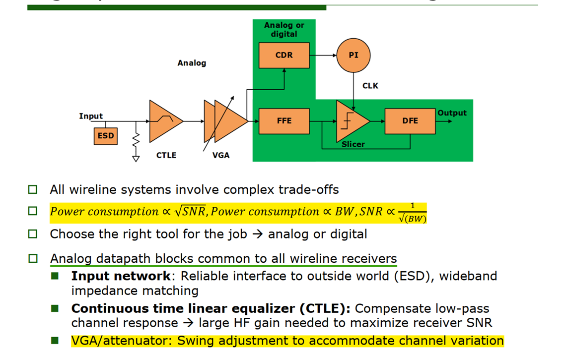
VGA/attenuator: ensure a constant swing at the slicer input regardless of the channel variation


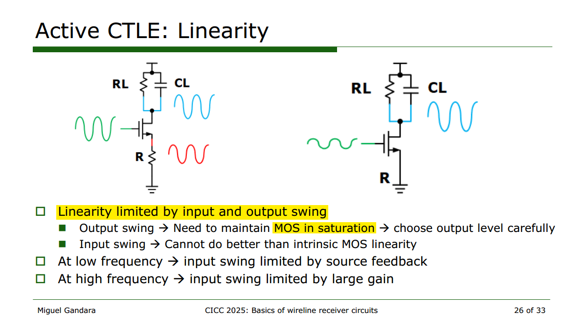
CTLE Linearity

TODO 📅

image-20260328182645140

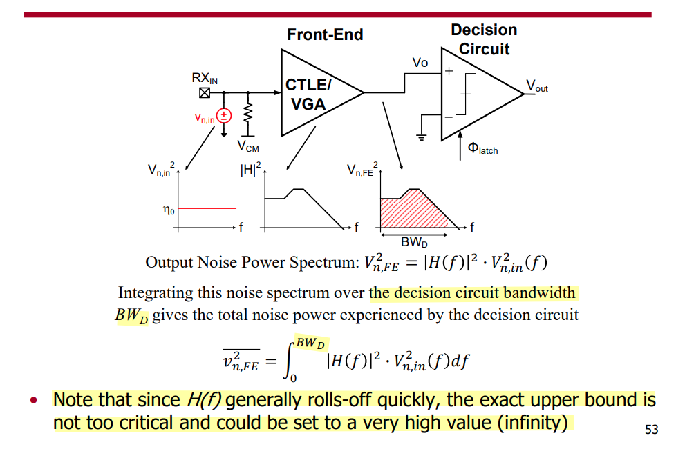
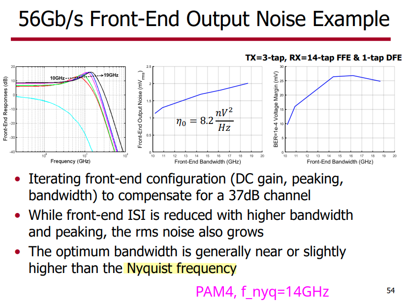
Front-End Noise

https://people.engr.tamu.edu/spalermo/ecen689/lecture6_ee720_rx_circuits.pdf

image-20250726180326659

image-20250726181859362

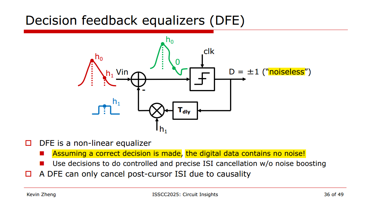
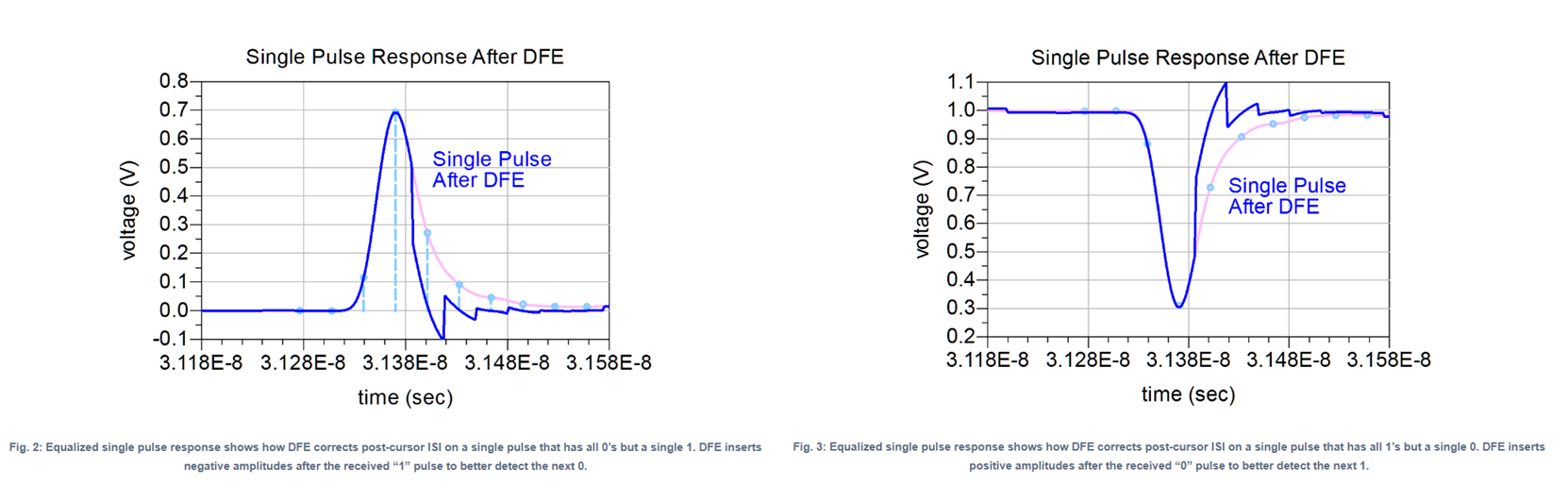
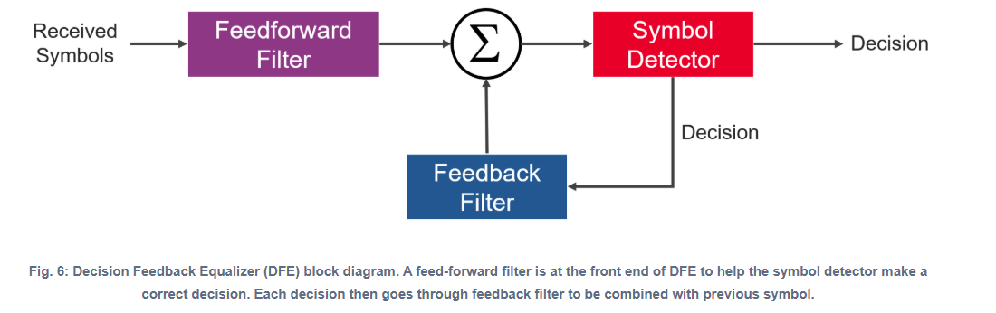
Decision Feedback Equalizer (DFE)

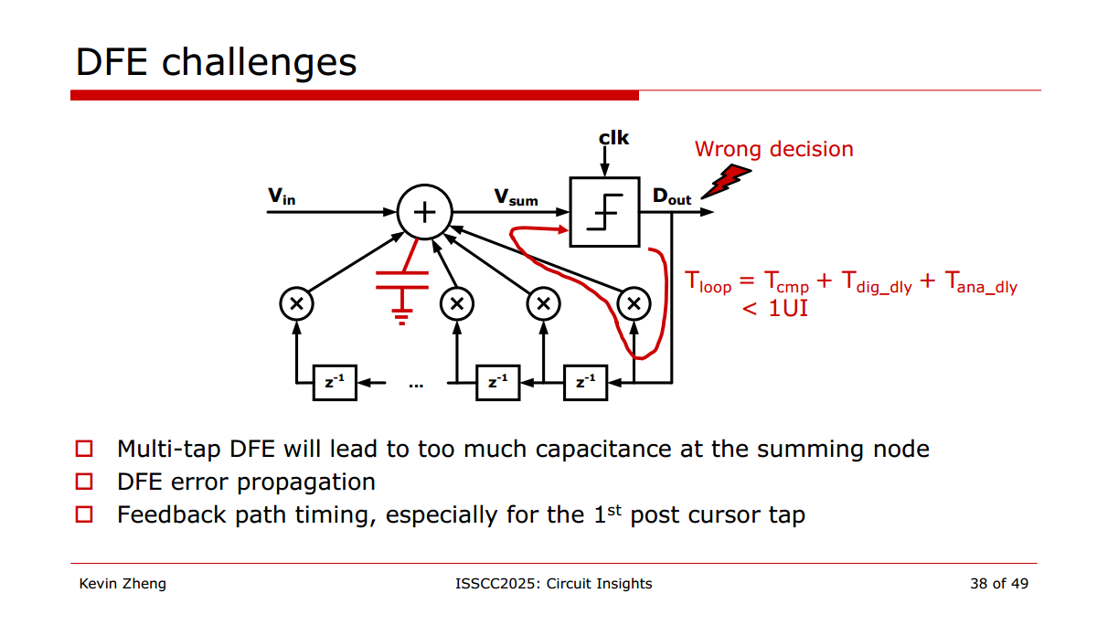
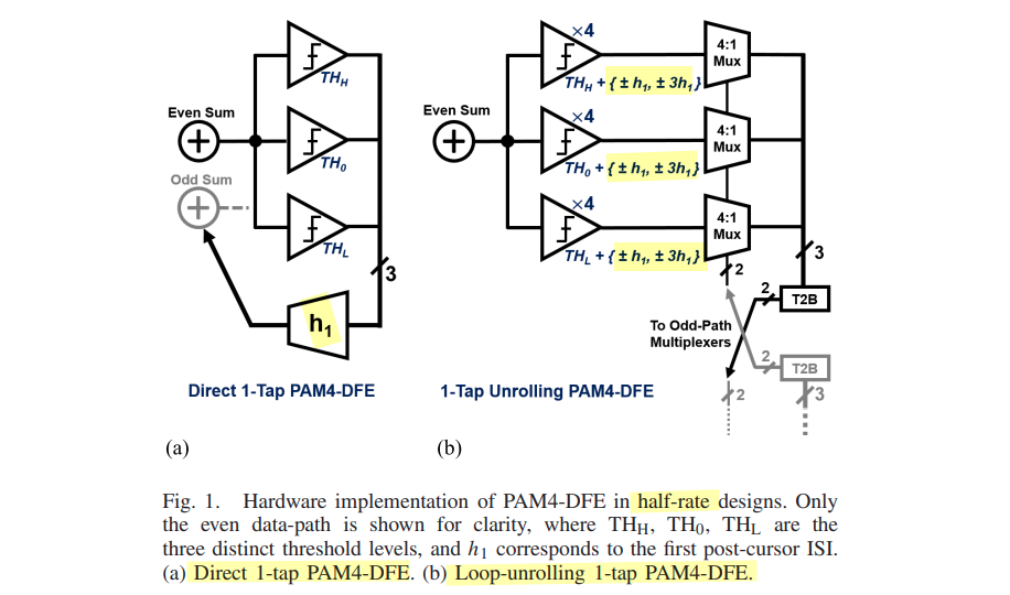
speculative DFE is also known as loop unrolled DFE, which solve the critical timing on first tap

DFE architecture

image-20260328182441169

image-20250607235201147

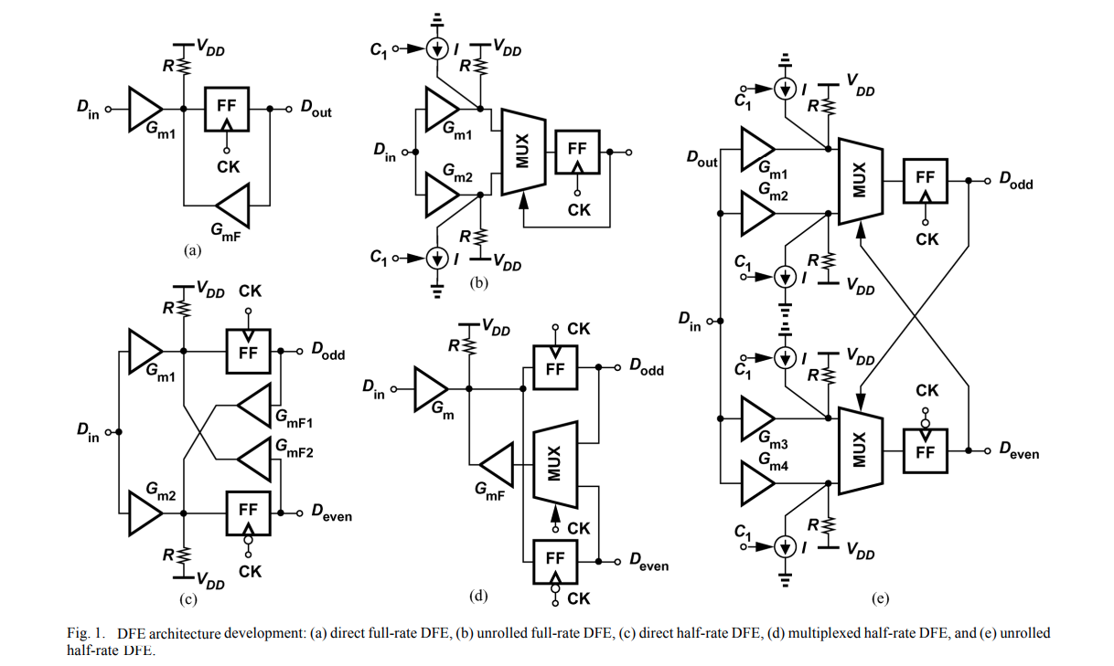
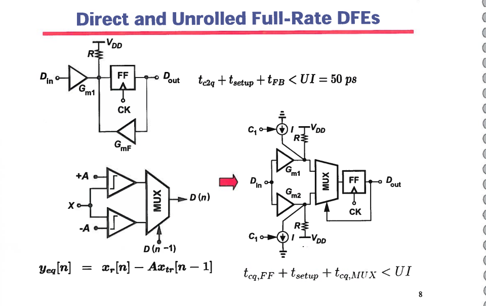
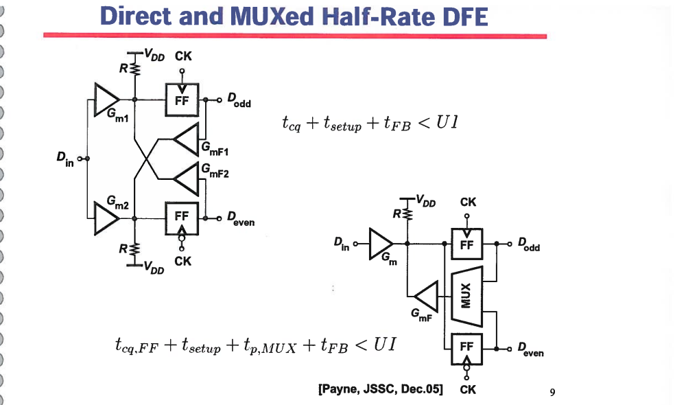
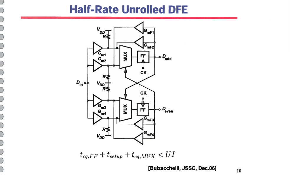
Extensive work on DFEs has produced a multitude of architectures, which can be broadly categorized as "direct"" or "unrolled" (speculative) DFEs with "full-rate" or "half-rate" clocking

image-20250608000306928

image-20250608000338808

image-20250608000357010

S. Ibrahim and B. Razavi, "Low-Power CMOS Equalizer Design for 20-Gb/s Systems," in IEEE Journal of Solid-State Circuits, vol. 46, no. 6, pp. 1321-1336, June 2011 [https://sci-hub.se/10.1109/JSSC.2011.2134450]

S. Ibrahim and B. Razavi, Low-Power DFE Design [https://picture.iczhiku.com/resource/eetop/wykflwIuIQDzYNcB.PDF]

DFE Error Propagation

Geoff Zhang. Preliminary Studies on DFE Error Propagation, Precoding, and their Impact on KP4 FEC Performance for PAM4 Signaling Systems [https://www.ieee802.org/3/ck/public/18_09/zhang_3ck_01a_0918.pdf]

Cathy Liu, The Effect of DFE Error Propagation [https://www.ieee802.org/3/ap/public/nov05/liu_01_1105.pdf]

Yuchun Lu, Huawei, Elimination of DFE Error Propagation and Post-FEC Error Floor (Precoding 2.0) [https://www.ieee802.org/3/ck/public/19_03/lu_3ck_01_0319.pdf]

Z. Wu and J. -R. Guo, "Analysis of UCIe 48/64 GT/s Electrical Links," in IEEE Open Journal of the Solid-State Circuits Society [pdf]

TODO 📅

image-20260328182254717

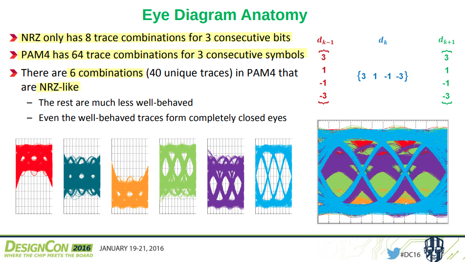
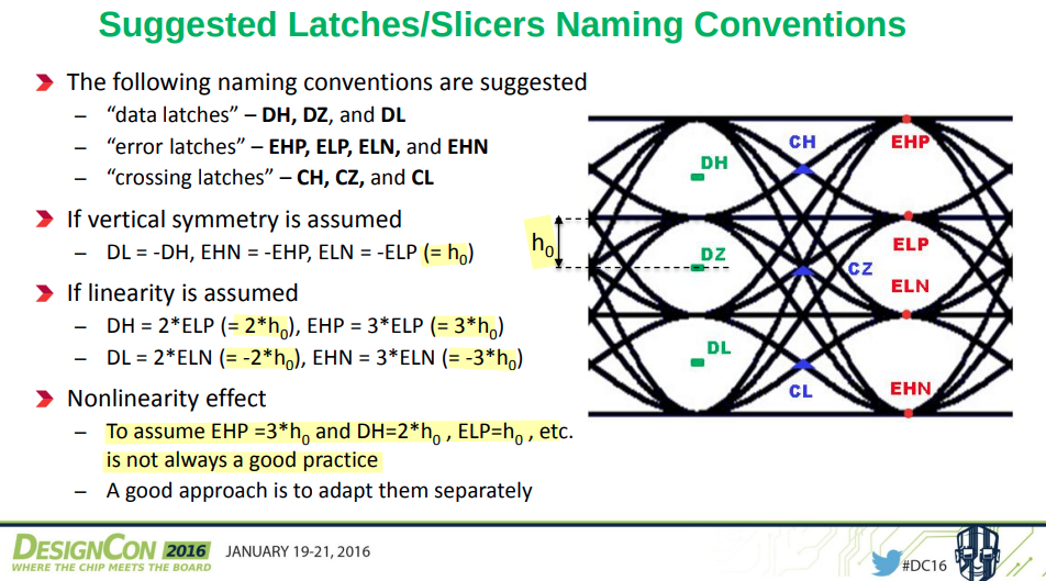
PAM4 DFE

image-20250525202236767

image-20250525210606180

image-20250525221556845

image-20250525221432513

image-20250525221148218

K. -C. Chen, W. W. -T. Kuo and A. Emami, "A 60-Gb/s PAM4 Wireline Receiver With 2-Tap Direct Decision Feedback Equalization Employing Track-and-Regenerate Slicers in 28-nm CMOS," in IEEE Journal of Solid-State Circuits, vol. 56, no. 3, pp. 750-762, March 2021 [https://www.mics.caltech.edu/wp-content/uploads/2021/02/JSSC-2020-Xavier-PAM4-Receiver.pdf]

Hongtao Zhang, DesignCon 2016. PAM4 Signaling for 56G Serial Link Applications − A Tutorial [https://www.xilinx.com/publications/events/designcon/2016/slides-pam4signalingfor56gserial-zhang-designcon.pdf]

Edge DFE

K. -L. J. Wong, E. -H. Chen and C. -K. K. Yang, "Edge and Data Adaptive Equalization of Serial-Link Transceivers," in IEEE Journal of Solid-State Circuits, vol. 43, no. 9, pp. 2157-2169, Sept. 2008 [[https://sci-hub.ru/10.1109/JSSC.2008.2001876]*https://sci-hub.ru/10.1109/JSSC.2008.2001876]

B. Brunn, “Edge equalization NRZ,” Jul. 2004 [Online]. Available: [http://www.ieee802.org/3/ap/public/jul04/brunn_01_0704.pdf]

CC Chen, "Why Edge DFE?" [https://youtu.be/azkm7A9plyY]

TODO 📅

reference

Miguel Gandara, MediaTek. CICC 2025 Circuit Insights: Basics of Wireline Receiver Circuits [https://youtu.be/X4JTuh2Gdzg]

Tony Chan Carusone, Alphawave Semi. VLSI2025 SC2: Connectivity Technologies to Accelerate AI

H. Park et al., "7.4 A 112Gb/s DSP-Based PAM-4 Receiver with an LC-Resonator-Based CTLE for >52dB Loss Compensation in 4nm FinFET," 2025 IEEE International Solid-State Circuits Conference (ISSCC), San Francisco, CA, USA, 2025

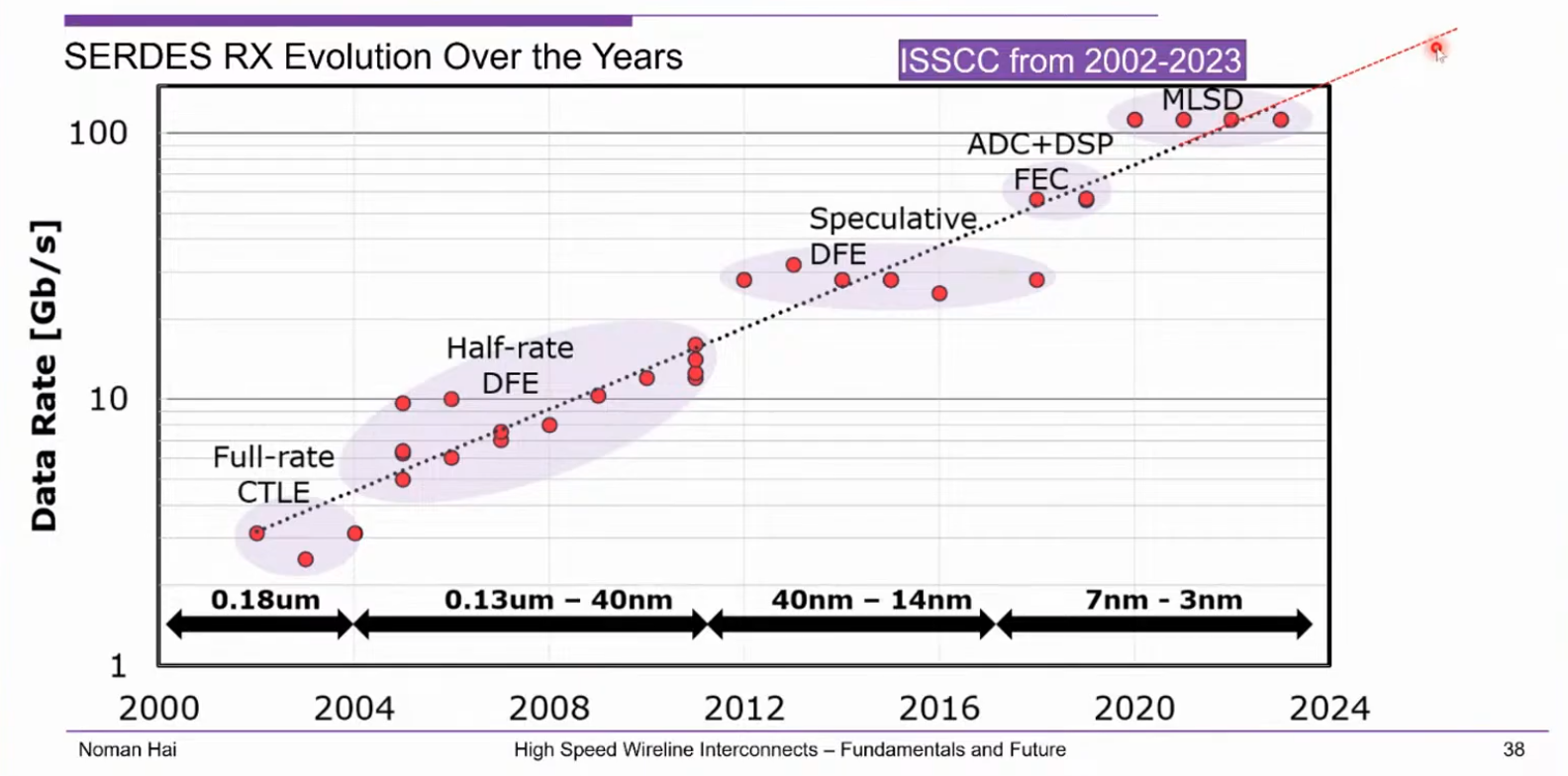
Noman Hai, Synopsys, Canada CASS Talks 2025 - May 2, 2025: High-speed Wireline Interconnects: Design Challenges and Innovations in 224G SerDes [https://www.youtube.com/live/wHNOlxHFTzY]

image-20260428003937326

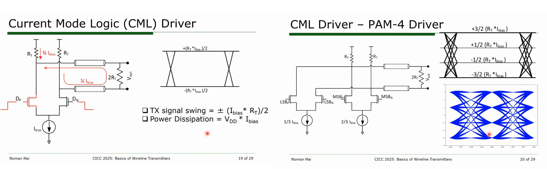
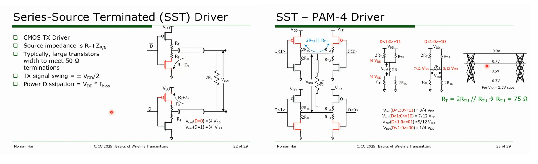
SST vs. CML Driver

Z. Toprak-Deniz et al., "A 128-Gb/s 1.3-pJ/b PAM-4 Transmitter With Reconfigurable 3-Tap FFE in 14-nm CMOS," in IEEE Journal of Solid-State Circuits, vol. 55, no. 1, pp. 19-26, Jan. 2020 [https://sci-hub.st/10.1109/JSSC.2019.2939081]

image-20260531080813258

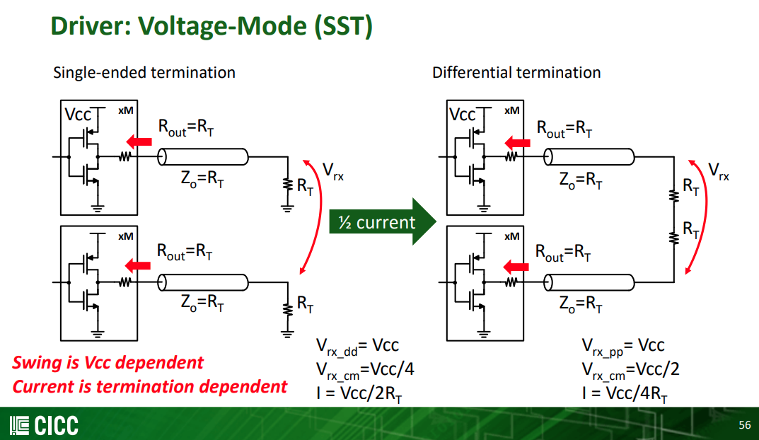
The source-series terminated (SST) drivers are more power-efficient than their current mode logic (CML) counterparts due to their lower termination power

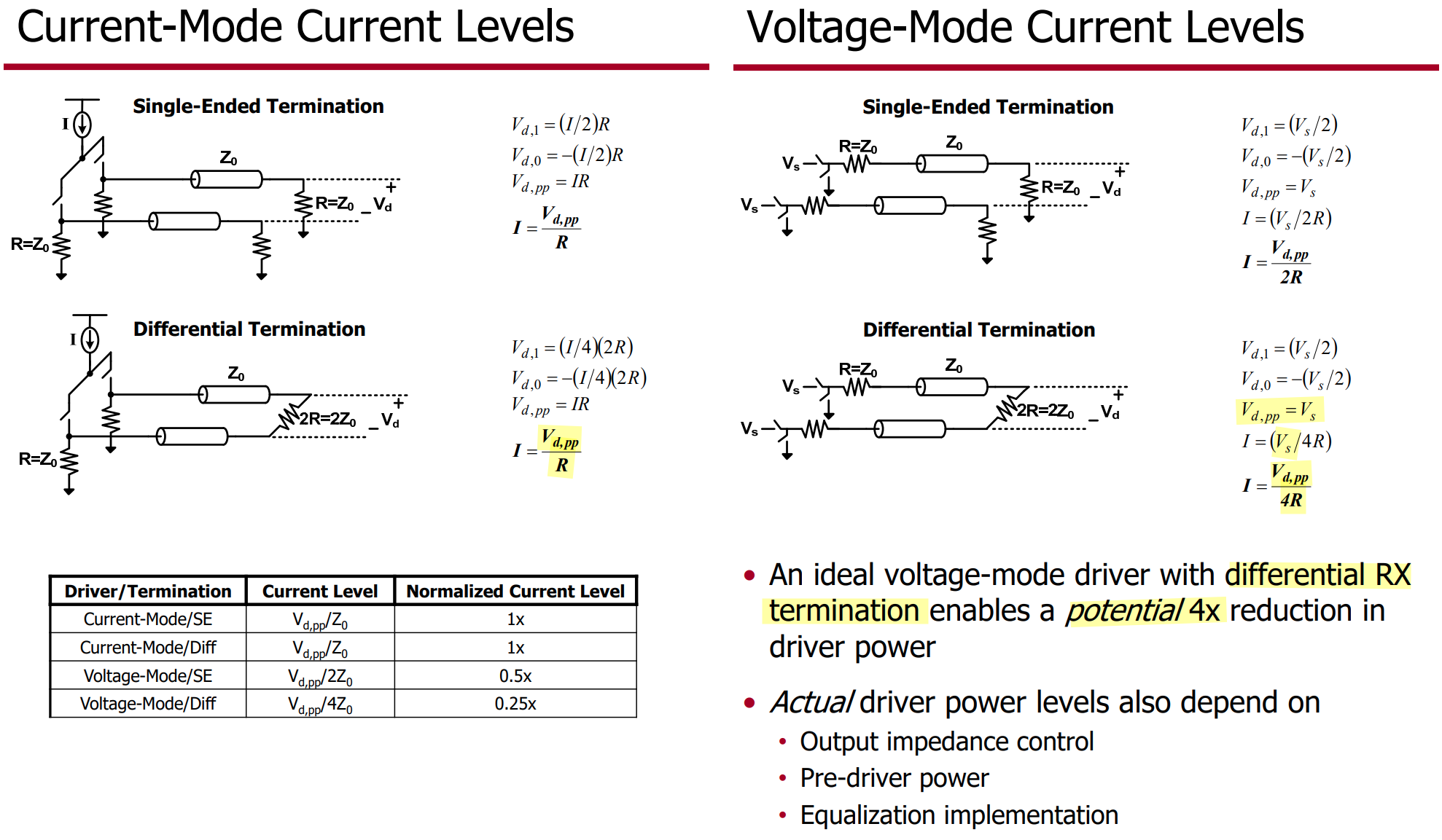
differential output amplitude

\[ V_{ad,SST} = \frac{V_{DD}}{4R_T}\cdot 2R_T = \boxed{I_{DD}\cdot 2R_T} \qquad V_{ad,CML} = \frac{I_{DD}}{4}\cdot 2R_T = \boxed{\frac{1}{4} I_{DD}\cdot 2R_T} \]

To achieve the same differential output amplitude, CML topologies consume \(4\) times the current of SST topologies

Serialization

Z. Toprak-Deniz et al., "A 128-Gb/s 1.3-pJ/b PAM-4 Transmitter With Reconfigurable 3-Tap FFE in 14-nm CMOS," in IEEE Journal of Solid-State Circuits, vol. 55, no. 1, pp. 19-26, Jan. 2020 [https://sci-hub.st/10.1109/JSSC.2019.2939081]

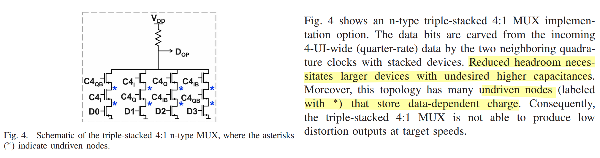
triple-stacked 4:1 n-type MUX

image-20260530063153678

tripstack4to1MUX.drawio

mux timing

mux2-1.drawio

divider latch timing

div2-latch.drawio

Two latches

two-latch.drawio

1UI Data Staggering

TODO 📅

1UI Pulse Generator

duty correction & delay adjustment

TODO 📅

Eye Linearity vs. RLM (Relative Level Mismatch)

TODO 📅

Chaowaroj (Max) Wanotayaroj. Introduction to PAM4 [https://indico.cern.ch/event/979659/contributions/4127016/attachments/2159338/3642883/PAM4Eval%20-%20Dec2020%20Seminar.pdf]

CML vs. SST based driver

image-20240825194548697

Design Challenges Of High-Speed Wireline Transmitters [https://semiengineering.com/design-challenges-of-high-speed-wireline-transmitters/]

image-20250607090928137

image-20250607091140352

the resistance of MOS is not highly controlled -> \(R_T + Z_N\)

image-20250607091858740

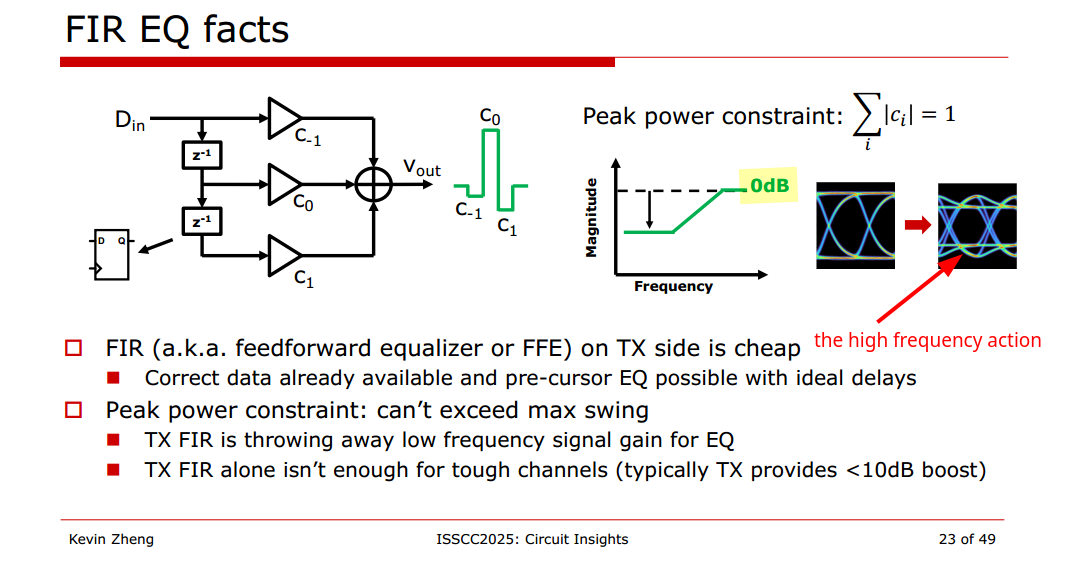
Peak power constraint of TX FIR

image-20250514215647905

Due to circuit limitation, circuit cannot have arbitrarily large voltage on the output, i.e. a limited maximum swing. In order to create the high frequency shape, the best we can do is lower DC gain (low frequency gain < 1)

  • FIR is not increasing the amplitude on the edges
  • FIR is reducing the inner eye diagram

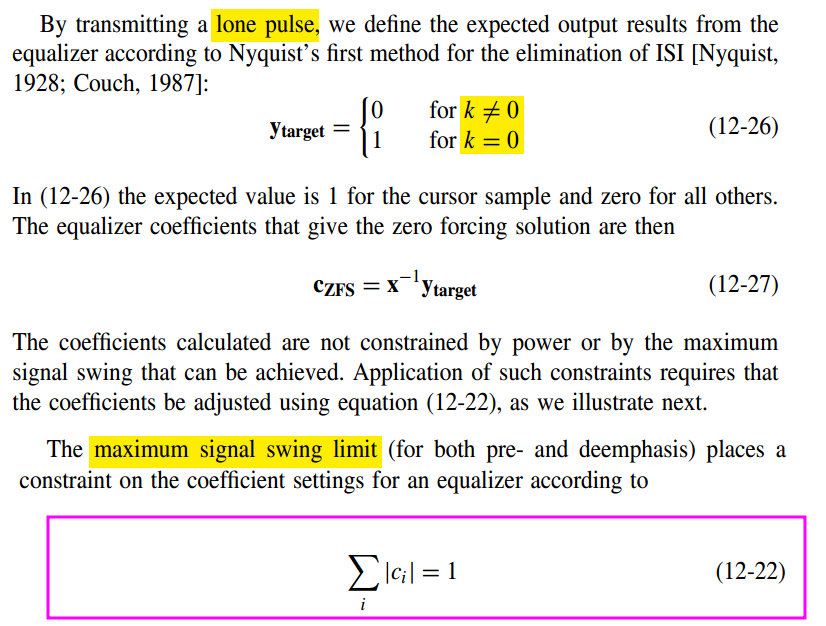
The maximum swing stays the same, \(\sum_i |c_i|=1\)

Circuit Insights @ ISSCC2025: Circuits for Wireline Communications - Kevin Zheng [https://youtu.be/8NZl81Dj45M&t=829]

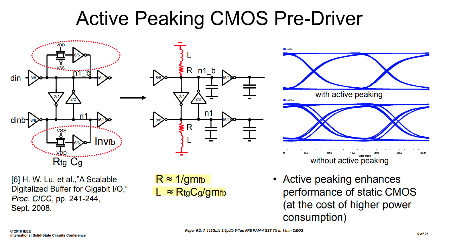
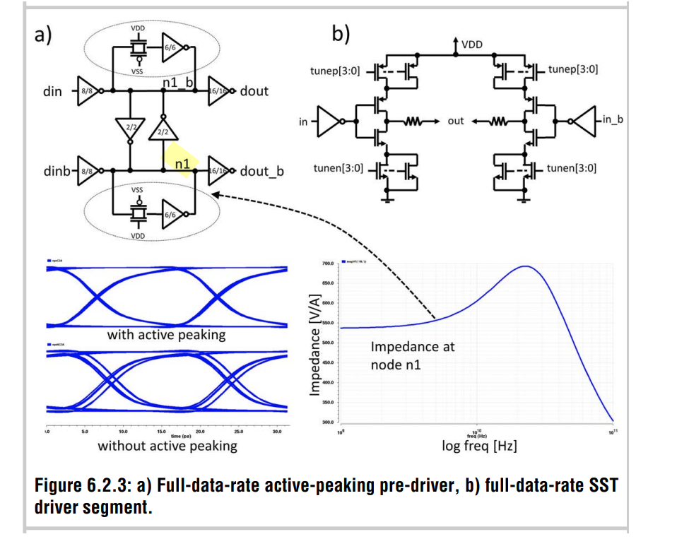
Active Peaking CMOS Pre-Driver

C. Menolfi et al., "A 112Gb/S 2.6pJ/b 8-Tap FFE PAM-4 SST TX in 14nm CMOS," 2018 IEEE International Solid-State Circuits Conference - (ISSCC), San Francisco, CA, USA, 2018, pp. 104-106 [slides paper]

image-20251217231605595

image-20251217231902887

SST Driver

sharing termination in SST transmitter

tx_leg.drawio

Sharing termination keep a constant current through leg, which improve TX speed in this way. On the other hand, the sharing termination facilitate drain/source sharing technique in layout.

pull-up and pull-down resistor

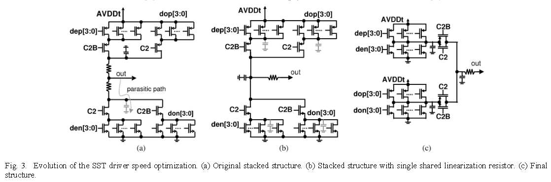
sst-evolution

Original stacked structure

Pro's:

​ smaller static current when both pull up and pull down path is on

Con's:

​ slowly switching due to parasitic capacitance behind pull-up and pull-down resistor

with single shared linearization resistor

Pro's:

​ The parasitic capacitance behind the resistor still exists but is now always driven high or low actively

Con's:

​ more static current

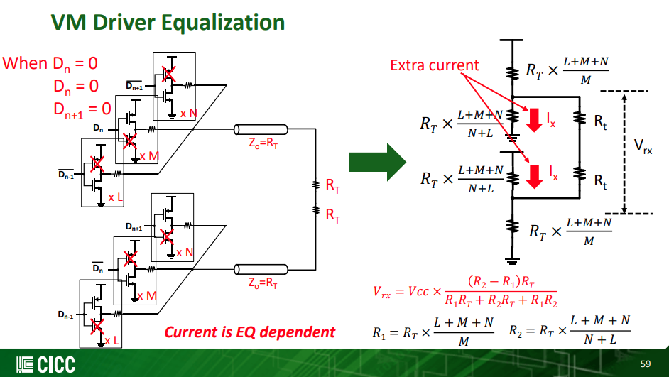
VM Driver Equalization - differential ended termination

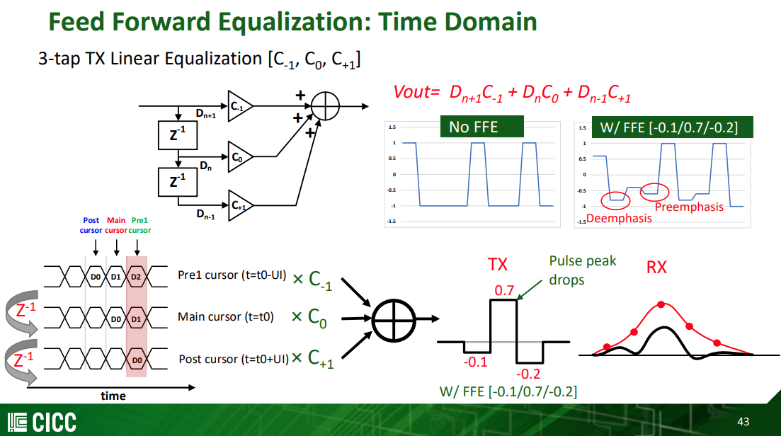
\[ V_o = D_{n+1}C_{-1}+D_nC_0+D_{n-1}C_{+1} \]

where \(D_n \in \{-1, 1\}\)

vdrv.drawio \[ V_{\text{rx}} = V_{\text{dd}} \frac{(R_2-R_1)R_T}{R_1R_T+R_2R_T+R_1R_2} \] With \(R_u=(L+M+N)R_T\)

Normalize above equation, obtain \[ V_{\text{rx,norm}} = \frac{(R_2-R_1)R_T}{R_1R_T+R_2R_T+R_1R_2} \]

\(D_{n-1}\) \(D_{n}\) \(D_{n+1}\)
\(C_{-1}\) 1 -1 -1
\(C_0\) -1 1 -1
\(C_{+1}\) -1 -1 1

Where precursor \(R_L = L\times R_T\), main cursor \(R_M = M\times R_T\) and post cursor \(R_N = N\times R_T\)

image-20220709151054840

Equation-1

\(D_{n-1}D_nD_{n+1}=1,-1,-1\)

pre.drawio

\[\begin{align} R_1 &= R_N \\ &= \frac{R_u}{N} \\ R_2 &= R_L\parallel R_M \\ &= \frac{R_u}{L+M} \end{align}\]

We obtain \[ V_{L}= \frac{1}{2}\cdot\frac{N-(L+M)}{L+M+N} \]

Equation-2

\(D_{n-1}D_nD_{n+1}=-1,1,-1\)

main.drawio

with \(R_1=R_T\) and \(R_2=+\infty\), we obtain \[ V_M = \frac{1}{2} \]

Equation-3

\(D_{n-1}D_nD_{n+1}=-1,-1,1\)

\[\begin{align} R_1 &= R_L \\ &= \frac{R_u}{L} \\ R_2 &= R_N\parallel R_M \\ &= \frac{R_u}{N+M} \end{align}\]

We obtain \[ V_N = \frac{1}{2}\cdot\frac{L-(N+M)}{L+M+N} \]

Obtain FIR coefficients

We define \[\begin{align} l &= \frac{L}{L+M+N} \\ m &= \frac{M}{L+M+N} \\ n &= \frac{N}{L+M+N} \end{align}\]

where \(l+m+n=1\)

Due to Eq1 ~ Eq3 \[ \left\{ \begin{array}{cl} C_{-1}-C_0-C_1 & = \frac{1}{2}(n-l-m) \\ -C_{-1}+C_0-C_1 & = \frac{1}{2} \\ -C_{-1}-C_0+C_1 & = \frac{1}{2}(l-n-m) \end{array} \right. \] After scaling, we get \[ \left\{ \begin{array}{cl} C_{-1}-C_0-C_1 & = -l-m+n \\ -C_{-1}+C_0-C_1 & = l+m+n \\ -C_{-1}-C_0+C_1 & = l-m-n \end{array} \right. \] Then, the relationship between FIR coefficients and legs is clear, i.e. \[\begin{align} C_{-1} &= -\frac{L}{L+M+N} \\ C_{0} &= \frac{M}{L+M+N} \\ C_{1} &= -\frac{N}{L+M+N} \end{align}\]

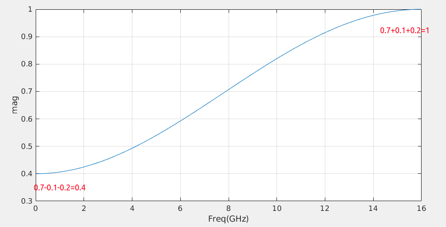
For example, \(C_{-1}=-0.1\), \(C_0=0.7\) and \(C_1=-0.2\) \[ H(z) = -0.1+0.7z^{-1}-0.2z^{-2} \] image-20220709185832444

1
2
3
4
5
6
7
w = [-0.1, 0.7, -0.2];
Fs = 32e9;
[mag, w] = freqz(w, 1, [], Fs);
plot(w/1e9, abs(mag));
xlabel('Freq(GHz)');
ylabel('mag');
grid on;

VM Driver Equalization - single ended termination

Equation-1

pre_se.drawio

\[\begin{align} V_{\text{rxp}} &= \frac{1}{2} \cdot \frac{N}{L+M+N} \\ V_{\text{rxm}} &= \frac{1}{2} \cdot \frac{L+M}{L+M+N} \end{align}\] So \[ V_{L}= \frac{1}{2}\cdot\frac{N-(L+M)}{L+M+N} \] which is same with differential ended termination

Equation-2

main_se.drawio

\[\begin{align} V_{\text{rxp}} &= \frac{1}{2} \\ V_{\text{rxm}} &= 0 \end{align}\] So \[ V_{M}= \frac{1}{2} \] which is same with differential ended termination

Equation-3

\[ V_{N}= \frac{1}{2}\cdot\frac{L-(N+M)}{L+M+N} \]

Obtain FIR coefficients

Same with differential ended termination driver.

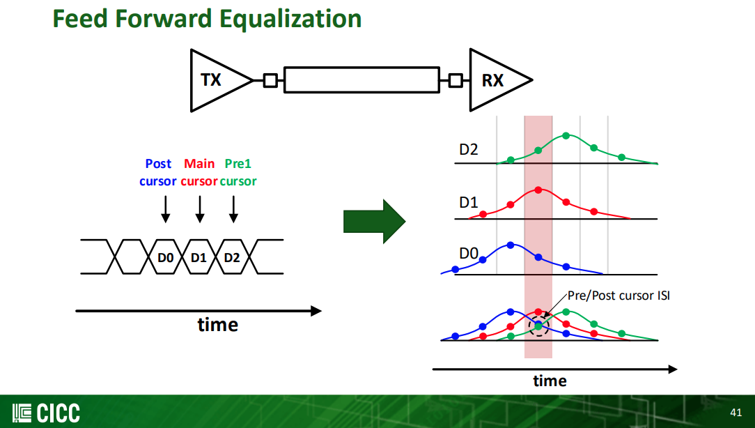
Basic Feed Forward Equalization Theory

image-20220709111229772

image-20220709112543338

image-20220709125046329

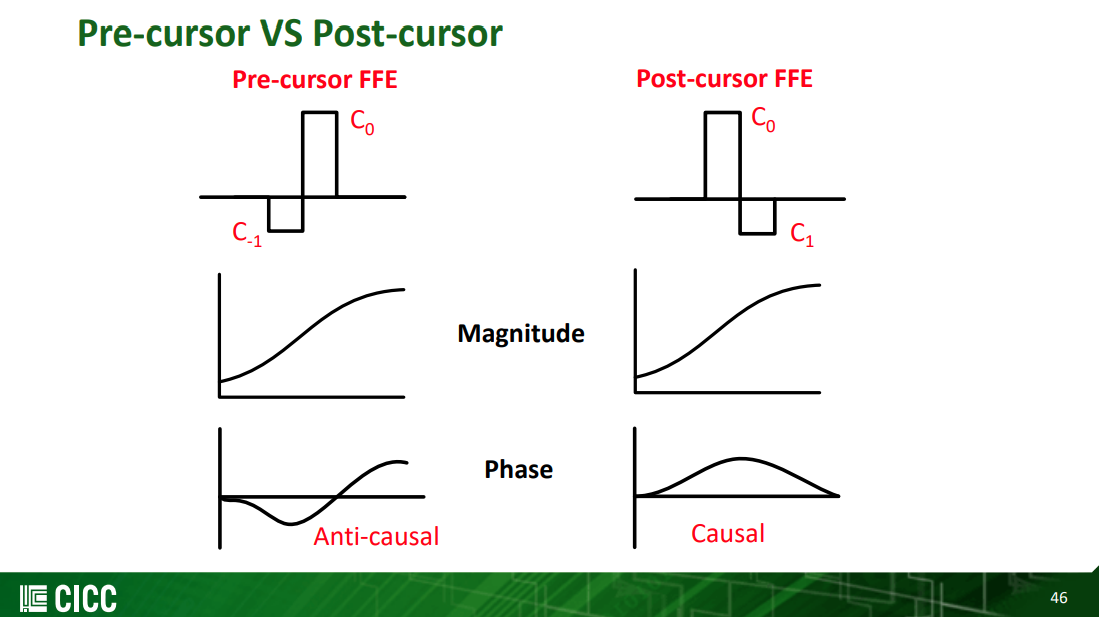
Pre-cursor FFE can compensate phase distortion through the channel

image-20220709130050057

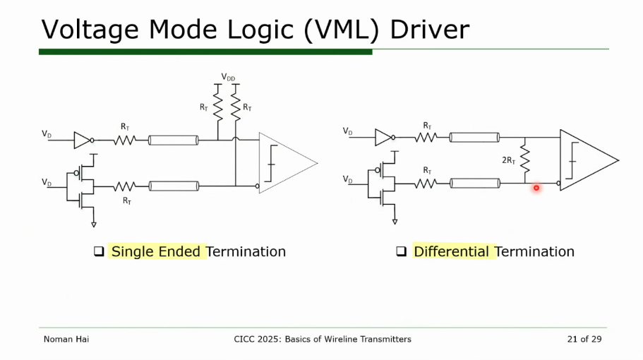
Single-ended termination

Differential termination

PAM4 TX

image-20220717010007963

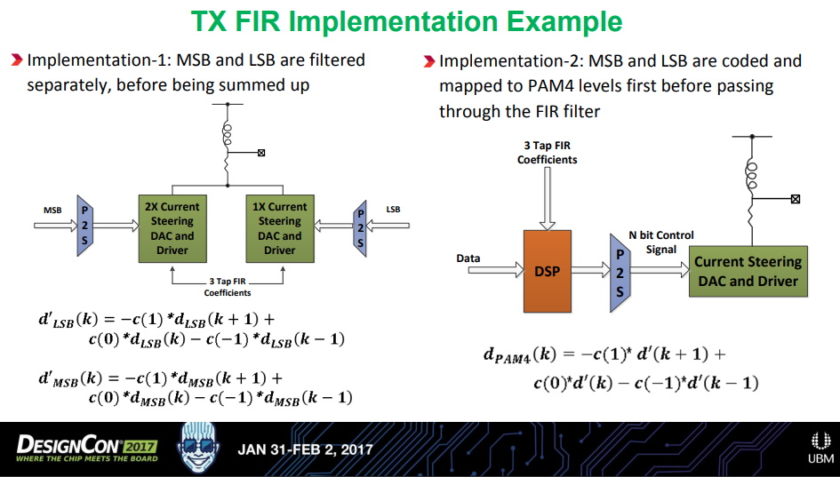
Here, \(d_{\text{LSB}} \in \{-1, 1\}\), \(d_{\text{MSB}} \in \{-2, 2\}\) and \(d' \in \{ -3, -1, 1, 3 \}\)

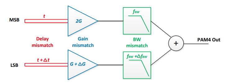
Implementation-1 could potentially experience performance degradation due to

  1. Clock skew, \(\Delta t\), could make the eye misaligned horizontally
  2. Gain mismatch, \(\Delta G\), could cause eye nonlinearity
  3. Bandwidth mismatch, \(\Delta f_{\text{BW}}\), could make the eye misaligned vertically

image-20220717011129124

Typically, a 3-tap FIR (pre + main + post) TX de-emphasis is used

3-tap FIR results in \(4^3 = 64\) possible distinct signal levels

msb_lsb.drawio

\[\begin{align} R_U^M \parallel R_D^M &= \frac{3R_T}{2}\\ R_U^L \parallel R_D^L &= 3R_T \end{align}\]

Thevenin Equivalent Circuit is thevenin_1.drawio

Which can be simpified as thevenin_2.drawio \[\begin{align} V_{\text{rx}} &= \frac{1}{2}(V_p - V_m) \\ &= \frac{1}{2}(\frac{2}{3}(2V_{\text{MSB}}+V_{\text{LSB}})-1) \\ &=\frac{1}{3}(2V_{\text{MSB}}+V_{\text{LSB}})-\frac{1}{2} \end{align}\]

The above eqations demonstrate that the output \(V_{\text{rx}}\) is the linear sum of MSB and LSB; LSB and MSB have relative weight, i.e. 1 for LSB and 2 for MSB.

Assume pre cusor has \(L\) legs, main cursor \(M\) legs and post cursor \(N\) legs, which is same with the convention in "Voltage-Mode Driver Equalization"

The number of legs connected with supply can expressed as \[ n_{up} = (1-d_{n+1})L + d_{n}M + (1-d_{n-1})N \] Where \(d_n \in \{0, 1\}\), or \[ n_{up} = \frac{1}{2}(-D_{n+1}+1)L + \frac{1}{2}(D_{n}+1)M + \frac{1}{2}(-D_{n-1}+1)N \] Where \(D_n \in \{-1, +1\}\)

Then the number of legs connected with ground is \[ n_{dn}=L+M+N-n_{up} \] where \(n_{up}+n_{dn}=L+M+N\)

Voltage resistor divider \[\begin{align} V_o &= \frac{\frac{R_{U}}{n_{dn}}}{\frac{R_U}{n_{dn}}+\frac{R_U}{n_{up}}} \\ &= \frac{1}{2}- \frac{1}{2}D_{n+1}\frac{L}{L+M+N}+ \frac{1}{2}D_{n}\frac{M}{L+M+N}-\frac{1}{2}D_{n-1}\frac{N}{L+M+N} \\ &= \frac{1}{2}-\frac{1}{2}D_{n+1}\cdot l+ \frac{1}{2}D_{n}\cdot m-\frac{1}{2}D_{n-1}\cdot n \end{align}\]

where \(l+m+n=1\)

\(V_{\text{MSB}}\) and \(V_{\text{LSB}}\) can be obtained

\[\begin{align} V_{\text{MSB}} &= \frac{1}{2}-\frac{1}{2}D^{\text{MSB}}_{n+1}\cdot l+ \frac{1}{2}D^{\text{MSB}}_{n}\cdot m-\frac{1}{2}D^{\text{MSB}}_{n-1}\cdot n \\ V_{\text{LSB}} &= \frac{1}{2}-\frac{1}{2}D^{\text{LSB}}_{n+1}\cdot l+ \frac{1}{2}D^{\text{LSB}}_{n}\cdot m-\frac{1}{2}D^{\text{LSB}}_{n-1}\cdot n \end{align}\]

Substitute the above equation into \(V_{\text{rx}}\), we obtain the relationship between driver legs and FFE coefficients

\[\begin{align} V_{\text{rx}} &=\frac{1}{3}(2V_{\text{MSB}}+V_{\text{LSB}})-\frac{1}{2} \\ &= \frac{1}{3} \left\{ 2\left( \frac{1}{2}-\frac{1}{2}D^{\text{MSB}}_{n+1}\cdot l+ \frac{1}{2}D^{\text{MSB}}_{n}\cdot m- \frac{1}{2}D^{\text{MSB}}_{n-1}\cdot n \right) + \left( \frac{1}{2}-\frac{1}{2}D^{\text{LSB}}_{n+1}\cdot l+ \frac{1}{2}D^{\text{LSB}}_{n}\cdot m- \frac{1}{2}D^{\text{LSB}}_{n-1}\cdot n \right) \right\}-\frac{1}{2} \\ &= \left(-\frac{l}{6} \cdot 2 \cdot D^{\text{MSB}}_{n+1}+ \frac{m}{6} \cdot 2 \cdot D^{\text{MSB}}_{n}- \frac{n}{6} \cdot 2 \cdot D^{\text{MSB}}_{n-1}\right) + \left(-\frac{l}{6} \cdot D^{\text{LSB}}_{n+1}+ \frac{m}{6} \cdot D^{\text{LSB}}_{n}- \frac{n}{6} \cdot D^{\text{LSB}}_{n-1}\right) \\ &= -\frac{l}{6}(2 \cdot D^{\text{MSB}}_{n+1}+D^{\text{LSB}}_{n+1})+ \frac{m}{6}(2\cdot D^{\text{MSB}}_{n}+D^{\text{LSB}}_{n}) -\frac{n}{6}(2\cdot D^{\text{MSB}}_{n-1}+D^{\text{LSB}}_{n-1}) \end{align}\]

After scaling, we obtain \[ V_{\text{rx}} = -l\cdot(2 \cdot D^{\text{MSB}}_{n+1}+D^{\text{LSB}}_{n+1})+ m\cdot(2\cdot D^{\text{MSB}}_{n}+D^{\text{LSB}}_{n}) - n \cdot(2\cdot D^{\text{MSB}}_{n-1}+D^{\text{LSB}}_{n-1}) \] Where \(C_{-1} = l\), \(C_0 = m\) and \(C_{1}=n\), which is same with that of NRZ

Tx Measurements

PAM4 Transmitter Test Challenges [https://harrisburg.psu.edu/files/pdf/16861/2019/05/06/tektronix_penn_state_si_april_12_2019.pdf]

PAM4 Signaling in High Speed Serial Technology: Test, Analysis, and Debug [https://download.tek.com/document/55W_60273_1_HR_Letter.pdf]

PCIe 7.0 Introduction PCIe 6.0 Anritsu/Tektronix Solution [https://map-assets.tek.com/map-assets/emea/pdf-files/PCIe7_0_Intro_PCIe_6_0_Solution.pdf]

Mike Hertz, Teledyne LeCroy: WEBINAR PAM4 Analysis and Measurement Considerations

Brandon Gore, Samtec, DesignCon 2025, Transmitter Power Spectral Density Noise Impact for 200 Gb/s PAM 4 per lane [pdf] [slides]

TODO 📅

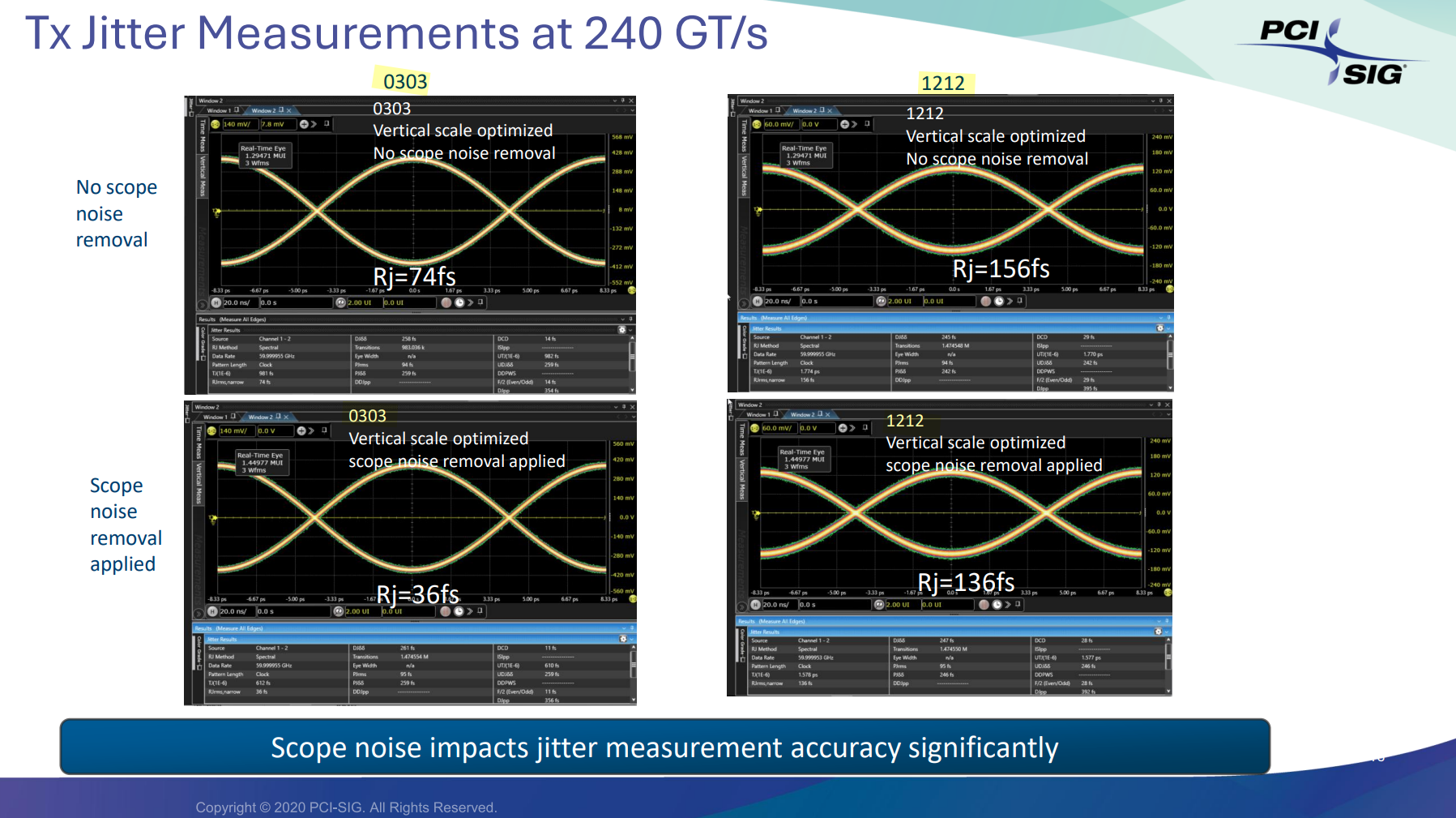
TX Jitter Measurement

PCI-SIG, Update-on-PCIe8p0-Scope-bandwidth-study-and-jitter-measurement-Intel-2025-12-18_v3

image-20260426211026901

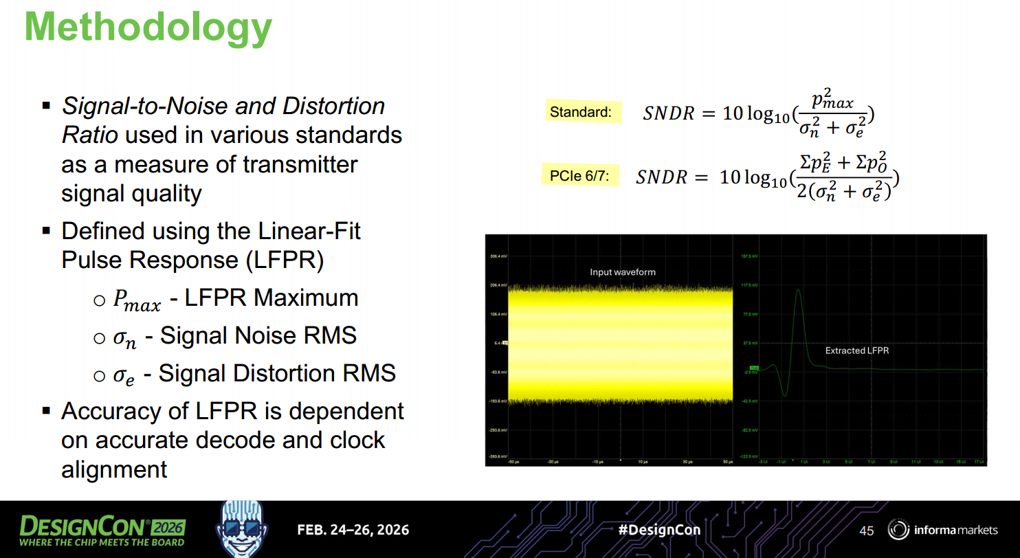
Linear Fit Pulse Response (LFPR)

Hsinho Wu, Intel. DesignCon 2021: SNDR Analysis & Its Impacts on Link Performance

Christiaan Bil (Intel), DesignCon 2026. An Experimental Study of PCIe Transmitter Equalization Preset Measurement Methods for 64 and 128 GT/s PAM4 Signaling

Dhruv Gupta, DesignCon 2026. PAM4 measurements through lossy channels – why oscilloscope CDR emulation matters

TODO 📅

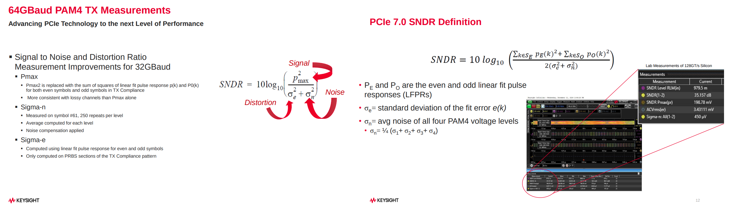
SNDR

Marianne Nourzad, July 2nd, 2020 PCI-SIG ® EWG Meeting, PCIE Gen6 TX SNDR Methodology Discussion

Pegah Alavi (Keysight Technologies) DesignCon 2025: PCI Express & PAM4: Balancing Silicon and interconnect interdependencies for 128 GT/s

Rick Eads, Pegah Alavi, Randy Garrett, Keysight Technologies) DesignCon 2025, The Road to PCIe 7.0: Advanced Testing Challenges at 64 GBaud PAM4 [https://www.keysight.com/us/en/assets/9925-01141/seminar-materials/KEF-DesignCon-2025-PCIe-Eads-Presentation.pdf]

image-20260607090715624

image-20260427232519514

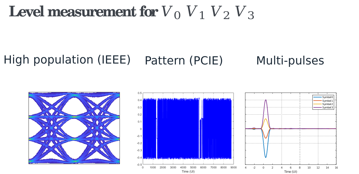
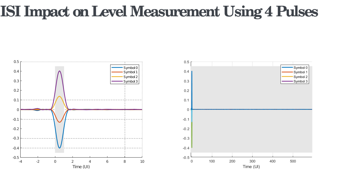
RLM Measurement Based on Multi-pulse Extraction

image-20260427224538461

image-20260427224752487

reference

Noman Hai, Synopsys. CICC 2025 Circuit Insights: Basics of Wireline Transmitter Circuits [https://youtu.be/oofViBGlrjM]

—, Synopsys. Design Challenges Of High-Speed Wireline Transmitters [https://semiengineering.com/design-challenges-of-high-speed-wireline-transmitters/]

—, Synopsys. CMOS Circuit Techniques for Wireline Transmitters [https://www.synopsys.com/webinars/wireline-transmitters-part-1.html]

Jihwan Kim, ISSCC2019 F5: Design Techniques for a 112Gbs PAM-4 Transmitter

—, Intel, SNU Summer 2021 [Topic] "A 200Gb/s CMOS Transmitter: Challenges and Overcoming Design Techniques" [https://youtu.be/w3lb_1TwdeE]

—, CICC 2022, ES4-4: Transmitter Design for High-speed Serial Data Communications

Friedel Gerfers, ISSCC2021 T6: Basics of DAC-based Wireline Transmitters

Tod Dickson, IBM. High-Speed CMOS Serial Transmitters for 56-112Gb/s Electrical Interconnects [https://www.youtube.com/watch?v=g1pcZabsRNc]

B. Razavi, "Design Techniques for High-Speed Wireline Transmitters," in IEEE Open Journal of the Solid-State Circuits Society, vol. 1, pp. 53-66, 2021,[https://www.seas.ucla.edu/brweb/papers/Journals/BROJSSCSep21.pdf]


Yvain Thonnart, CEA-LIST. ISSCC2021 T8: On-Chip Interconnects: Basic Concepts, Designs and Future Opportunities

Mozhgan Mansuri. ISSCC2021 SC3: Clocking, Clock Distribution, and Clock Management in Wireline/Wireless Subsystems

Sam Palermo. High-Performance SERDES Design" Online Course (2025): Current-Mode DAC TX [https://youtu.be/A2VsvCPDWxk]

PCIe® 6.0 Specification: The Interconnect for I/O Needs of the Future PCI-SIG® Educational Webinar Series, [https://pcisig.com/sites/default/files/files/PCIe%206.0%20Webinar_Final_.pdf]

J. F. Bulzacchelli et al., "A 28-Gb/s 4-Tap FFE/15-Tap DFE Serial Link Transceiver in 32-nm SOI CMOS Technology," in IEEE Journal of Solid-State Circuits, vol. 47, no. 12, pp. 3232-3248, Dec. 2012, doi: 10.1109/JSSC.2012.2216414.

C. Menolfi et al., "A 112Gb/S 2.6pJ/b 8-Tap FFE PAM-4 SST TX in 14nm CMOS," 2018 IEEE International Solid - State Circuits Conference - (ISSCC), 2018, pp. 104-106, doi: 10.1109/ISSCC.2018.8310205.

E. Chong et al., "A 112Gb/s PAM-4, 168Gb/s PAM-8 7bit DAC-Based Transmitter in 7nm FinFET," ESSCIRC 2021 - IEEE 47th European Solid State Circuits Conference (ESSCIRC), 2021, pp. 523-526, doi: 10.1109/ESSCIRC53450.2021.9567801.

Wang, Z., Choi, M., Lee, K., Park, K., Liu, Z., Biswas, A., Han, J., Du, S., & Alon, E. (2022). An Output Bandwidth Optimized 200-Gb/s PAM-4 100-Gb/s NRZ Transmitter With 5-Tap FFE in 28-nm CMOS. IEEE Journal of Solid-State Circuits, 57(1), 21-31. https://doi.org/10.1109/JSSC.2021.3109562

J. Kim et al., "A 112Gb/s PAM-4 transmitter with 3-Tap FFE in 10nm CMOS," 2018 IEEE International Solid - State Circuits Conference - (ISSCC), 2018, pp. 102-104, doi: 10.1109/ISSCC.2018.8310204.

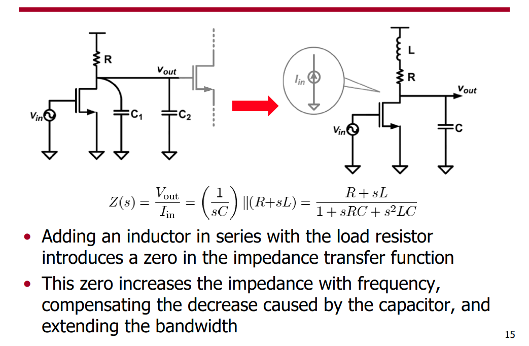
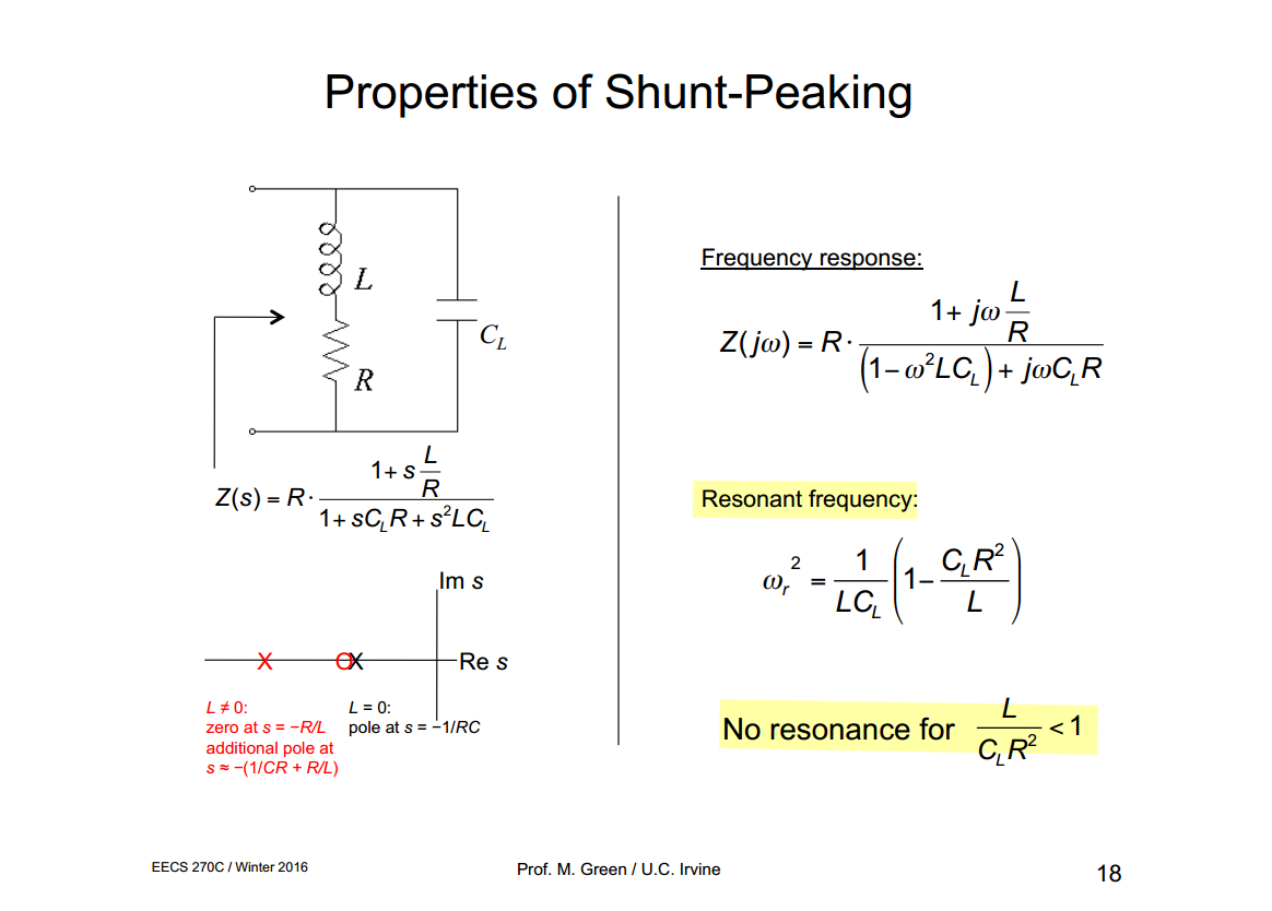
shunt peaking

image-20260608215130203

image-20251206000303668

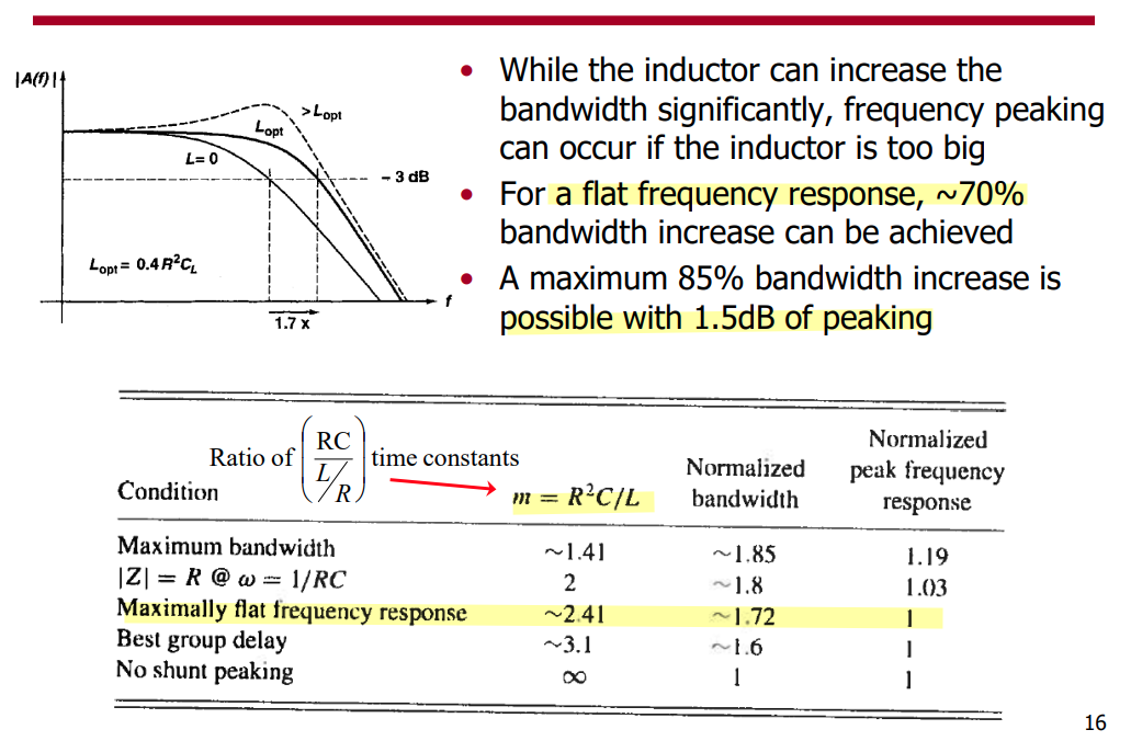
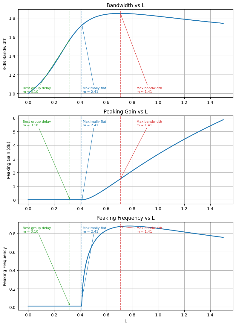
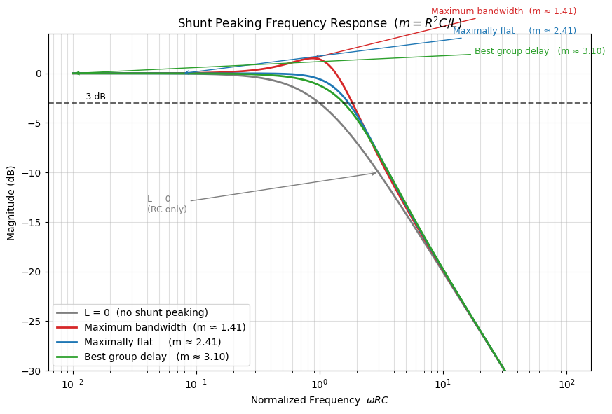
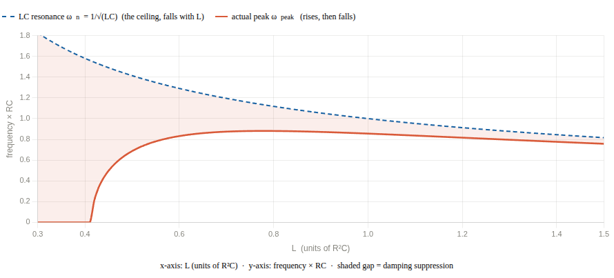
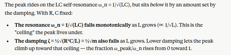
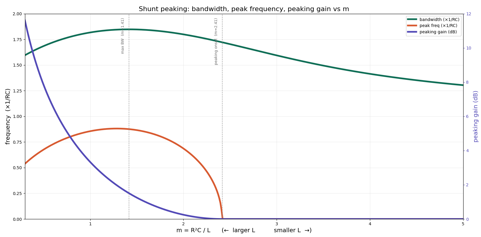
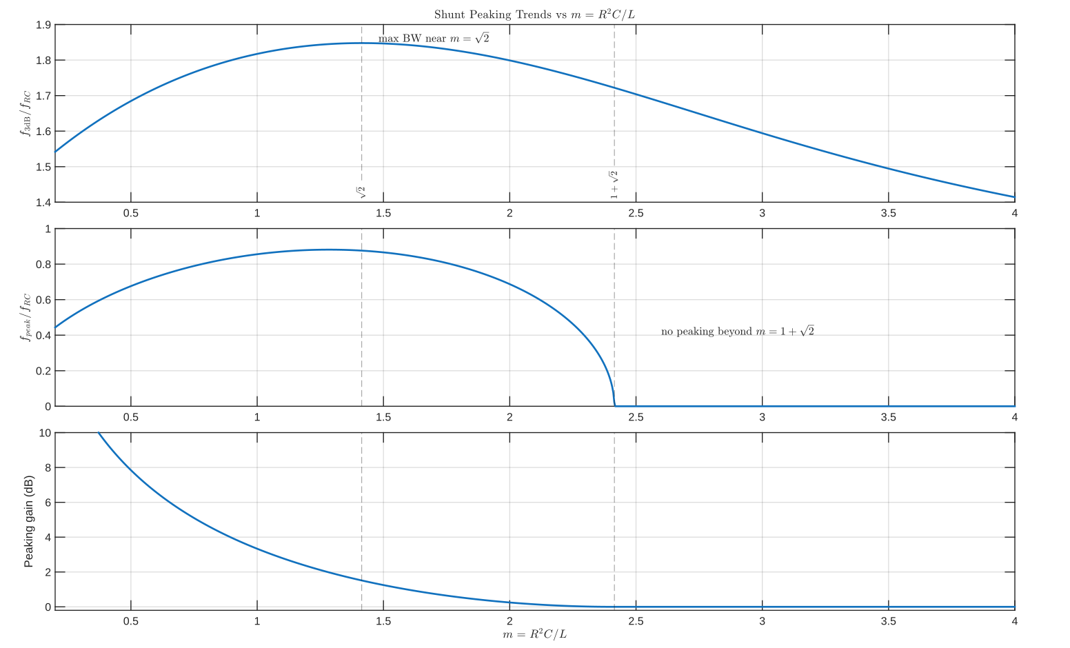
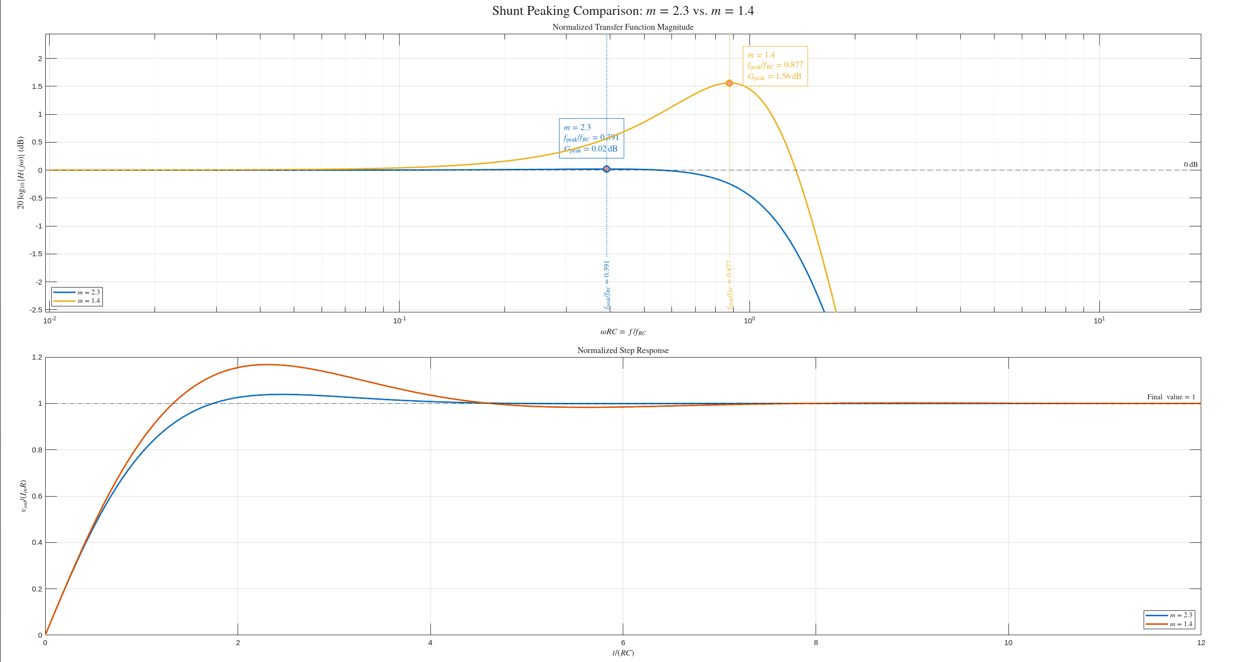
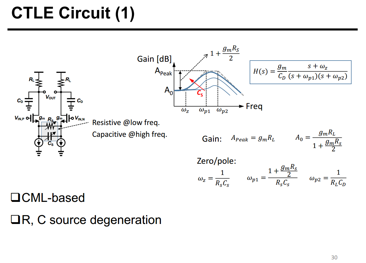
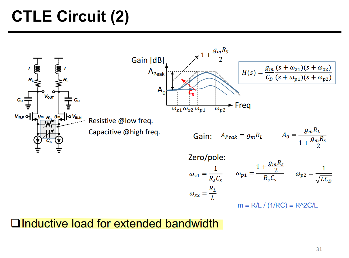
\(\color{red}m=\frac{R^2C}{L}\) is the ratio of the \(R/L\) zero frequency to the original RC pole frequency \(1/RC\), and therefore measures how aggressively the zero compensates the intrinsic RC roll-off.

[Gist link]

image-20260526211605905

image-20260526211624229

1
2
3
4
5
6
7
8
9
10
11
12
13
14
15
16
17
18
19
20
21
# Normalize R = C = 1
R = 1.0
C = 1.0

# Frequency sweep
w = np.logspace(-2, 2, 20000)

# Shunt peaking transfer function
#
# R + sL
# H(s) = ---------
# 1 + sRC + s^2 LC
#
# normalized low-frequency gain = 1
#
def H(jw, L):
s = 1j * jw
return (R + s*L) / (R + s*R*R*C + s*s*L*R*C)

# Sweep inductance
Lvals = np.linspace(0.001, 1.5, 300)

image-20260608220405307

image-20260608220440363

[Gist link]

image-20260608224954010

image-20260608224505556

image-20260608225657252


image-20260611225858681

image-20260611225951811

[Gist link]

shunt_chatgpt

image-20260611233156089

series peaking

image-20260526230433602

image-20260526230805917

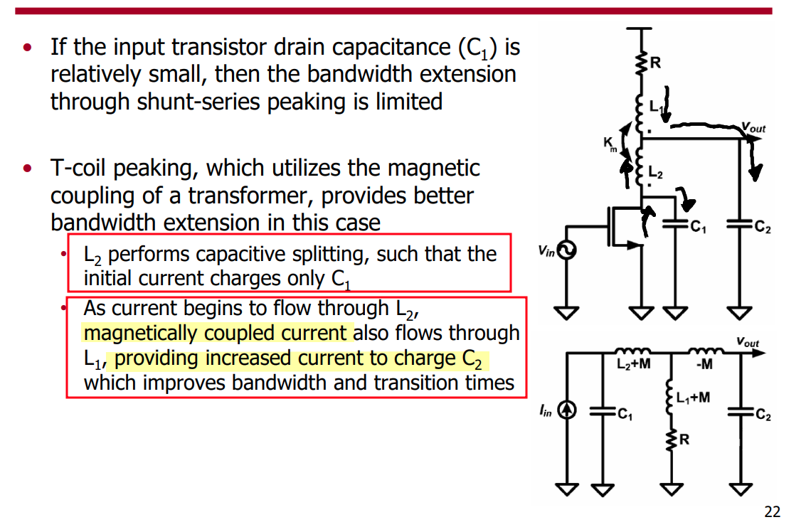
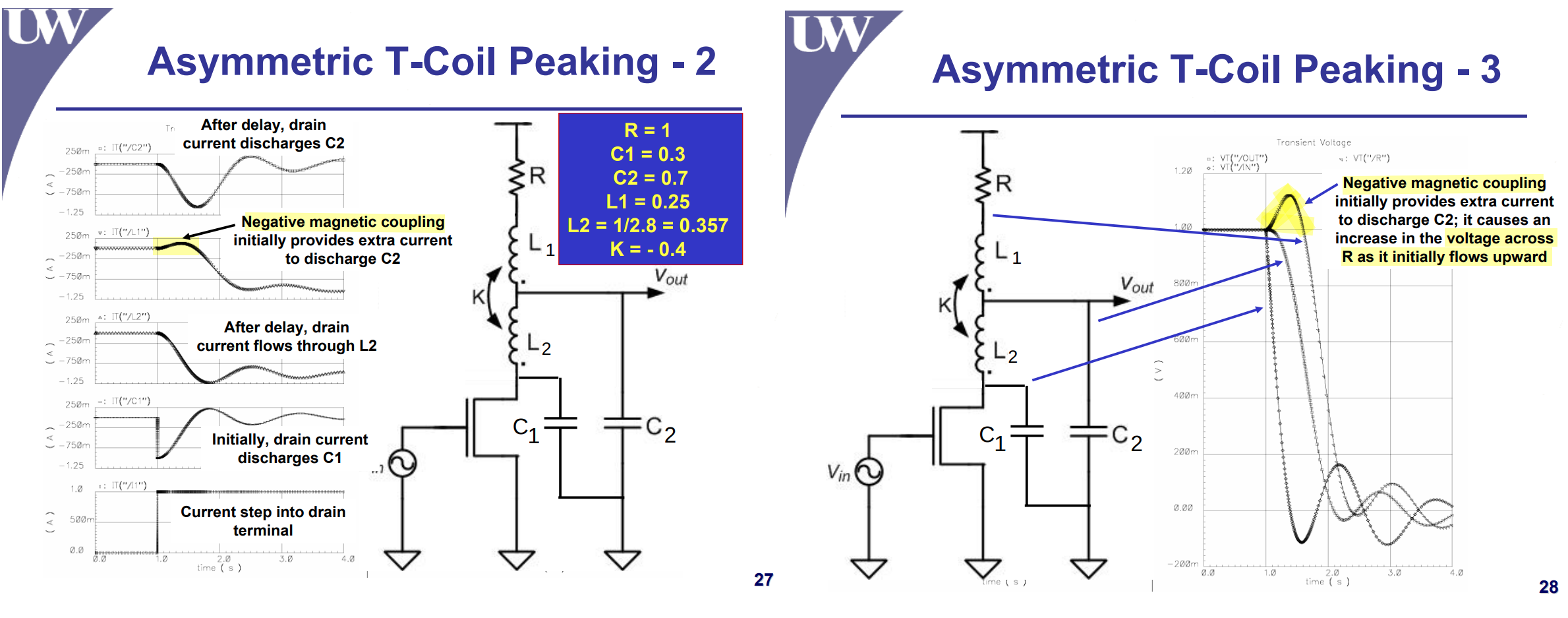
T-Coil Peaking

Jri Lee. ISSCC 2009 Tutorial. CMOS Circuit Techniques for High Speed Wireline Transceivers [http://cc.ee.ntu.edu.tw/~jrilee/course/2009_Tutorial_10.pdf]

CC Chen. Why SerDes Needs a Rule of Thumb for T-Coil Design? [https://youtu.be/RIQLYQG2u0A]

Capacitor Splitting + Magnetic Coupling of a transformer

image-20251022234854155

image-20251022235133839

tcoil-tran.drawio


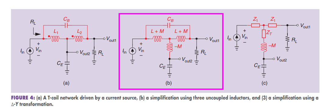
alternative analysis with the below 3 uncoupled inductors model

tcoil-tran-3L.drawio


Three uncoupled inductors model

image-20251126173130097

tcoil-Y.drawio \[\begin{align} V_{P13} &= I_1\cdot sL_1 + I_2\cdot sM = I_1\cdot s(L_1+M) + (I_1-I_2)\cdot s(-M) \\ V_{P23} &= -I_2\cdot sL_2 - I_1\cdot sM = -I_2\cdot s(L_2 + M) + (I_1-I_2)\cdot s(-M) \end{align}\]

The negative inductor \(-M\) can be seen as capacitor \[ -j\omega M = \frac{1}{j}\omega M = \frac{1}{j\omega \frac{1}{\omega^2 M}} \] That is \(C_{-M} = \frac{1}{\omega^2 M} \approx 10 \times C_E\)


image-20260715221444331

T-coil w/ inverted mutual coupling

J. Kim, J. -K. Kim, B. -J. Lee and D. -K. Jeong, "Design Optimization of On-Chip Inductive Peaking Structures for 0.13- μm CMOS 40-Gb/s Transmitter Circuits," in IEEE Transactions on Circuits and Systems I: Regular Papers, vol. 56, no. 12, pp. 2544-2555, Dec. 2009 [https://sci-hub.st/10.1109/TCSI.2009.2023772]

TODO 📅

Triple Resonance

TODO 📅

image-20251206000718234


series resonance \(\omega_\text{res}\)

Assuming, \(I_\text{in}=\cos\omega_r t\) and \(V_\text{out}=g\cos(\omega_r t +\theta)\)

with \(I_\text{in} = C_L\frac{\mathrm{d}V_\text{out}}{\mathrm{d}t}\), yield \(g=\sqrt{\frac{L}{C}}\) and \(\theta=- \frac{\pi}{2}\), i.e. \(V_\text{out} = \sqrt{\frac{L}{C}}\cos(\omega_r t - \frac{\pi}{2})\)

Active Inductor

B. Razavi, "The Active Inductor [A Circuit for All Seasons]," in IEEE Solid-State Circuits Magazine, vol. 12, no. 2, pp. 7-11, Spring 2020 [https://www.seas.ucla.edu/brweb/papers/Journals/BR_SSCM_2_2020.pdf]
activeInd

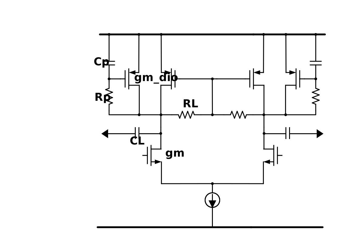
\[\begin{align} A &= \frac{g_mR_L}{1+(g_{\text{m}_{\text{dio}}}+ g_{\text{ds}_\text{tot}})R_L}\cdot \frac{1+R_pC_Ps}{1+\frac{(1+g_{\text{ds}_{\text{tot}}}R_L)R_PC_P+C_PR_L+R_LC_L}{1+(g_{\text{m}_{\text{dio}}}+g_{\text{ds}_\text{tot}})R_L}s + \frac{R_LC_LR_PC_P}{1+(g_{\text{m}_\text{dio}}+g_{\text{ds}_{\text{tot}}})R_L}s^2} \\ &= \frac{g_mR_L}{1+(g_{\text{m}_{\text{dio}}}+ g_{\text{ds}_{\text{tot}}})R_L}\cdot \frac{R_PC_P}{ \frac{R_LC_LR_PC_P}{1+(g_{\text{m}_{\text{dio}}}+g_{\text{ds}_{\text{tot}}})R_L}}\cdot \frac{1/(R_PC_P)+s}{s^2 + \frac{(1+g_{\text{ds}_{\text{tot}}}R_L)R_PC_P+C_PR_L+R_LC_L}{R_PC_P}s + \frac{1+(g_{\text{m}_{\text{dio}}}+g_{\text{ds}_\text{tot}})R_L}{R_LC_LR_PC_P}} \\ &= A_0 \cdot A(s) \end{align}\]

That is

\[\begin{align} \omega_z &= \frac{1}{R_PC_P} \tag{1} \\ \omega_n &= \sqrt{\frac{1+(g_{\text{m}_{\text{dio}}}+ g_{\text{ds}_\text{tot}})R_L}{R_LC_LR_PC_P}} = \sqrt{\omega_{p0}\omega_z} \\ \zeta & = \frac{(1+g_{\text{ds}_\text{tot}}R_L)R_PC_P+C_PR_L+R_LC_L}{R_PC_P} \frac{1}{2 \omega_n} \end{align}\]

Where \[\begin{align} \omega_{p0} &= \frac{1}{(R_L||\frac{1}{g_{\text{m}_{\text{dio}}}}||\frac{1}{g_{\text{m}_{\text{tot}}}})C_L} \tag{2} \end{align}\]

Here, relate \(\omega_{p0}\) and \(\omega_z\) by coefficient \(\alpha\) \[ \omega_{p0} = \alpha \cdot \omega_z \tag{3} \] This way \[ \omega_n= \sqrt{\alpha}\cdot \omega_z \]

\[ \zeta = \frac{1}{2}(K\sqrt{\alpha}+\frac{1+C_P/C_L}{\sqrt{\alpha}}) \tag{4} \]

where \[ K = \frac{R_L||\frac{1}{g_{\text{m}_{\text{dio}}}}||\frac{1}{g_{\text{m}_{\text{tot}}}}}{R_L||g_\text{ds\_tot}} \]

And \(A(s)\) can be expressed as \[ A(s) = \frac{\frac{s}{\omega_z}+1}{\frac{s^2}{\omega_n^2}+2\frac{\zeta}{\omega_n}s+1} \] It magnitude in dB \[ A_\text{dB} = 10\log\frac{1+(\omega/\omega_z)^2}{1+(\omega/\omega_n)^4+2\omega^2(2\zeta^2-1)/\omega_n^2} \] Substitute \(\omega_n\) with Eq (2), followed is obtained \[ A_\text{dB} = 10\log{\frac{\alpha^2(\omega_z^4 + \omega_z^2\omega^2)}{\alpha^2\omega_z^4+\omega^4+2\alpha\omega_z^2(2\zeta^2-1)\omega^2}} \] peaking frequency \[ \omega_\text{peak} = \omega_z\cdot \sqrt{\sqrt{(\alpha+1)^2 - 4\alpha \zeta^2}-1} \] If \(\zeta=1\) \[ \omega_{A_\text{dB = 0dB} } = \sqrt{1-2/\alpha}\cdot \omega_{p0} \qquad \omega_\text{peak} = \omega_z\sqrt{\alpha-2} \qquad A_\text{dB,peak} = 10\log\frac{\alpha^2}{4(\alpha-1)} \]

Negative Capacitance Circuit

Negative Miller Capacitance

S. Gondi and B. Razavi, "Equalization and Clock and Data Recovery Techniques for 10-Gb/s CMOS Serial-Link Receivers," in IEEE Journal of Solid-State Circuits, vol. 42, no. 9, pp. 1999-2011 [pdf]

Sam Palermo. ECEN620 Lecture 14: Limiting Amplifiers (LAs) [https://people.engr.tamu.edu/spalermo/ecen620/lecture14_ee620_limiting_amps.pdf]

image-20251028221403199

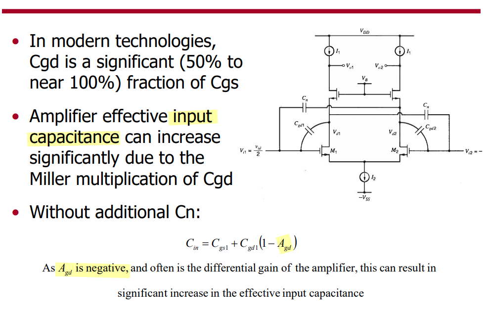
image-20251028232644575 \[ C_{d1} = C_{dd1} + (1+\frac{1}{|A_{gd}|})C_{gd1} \] where \(A_{gd}\lt 0\)

image-20251028232707189

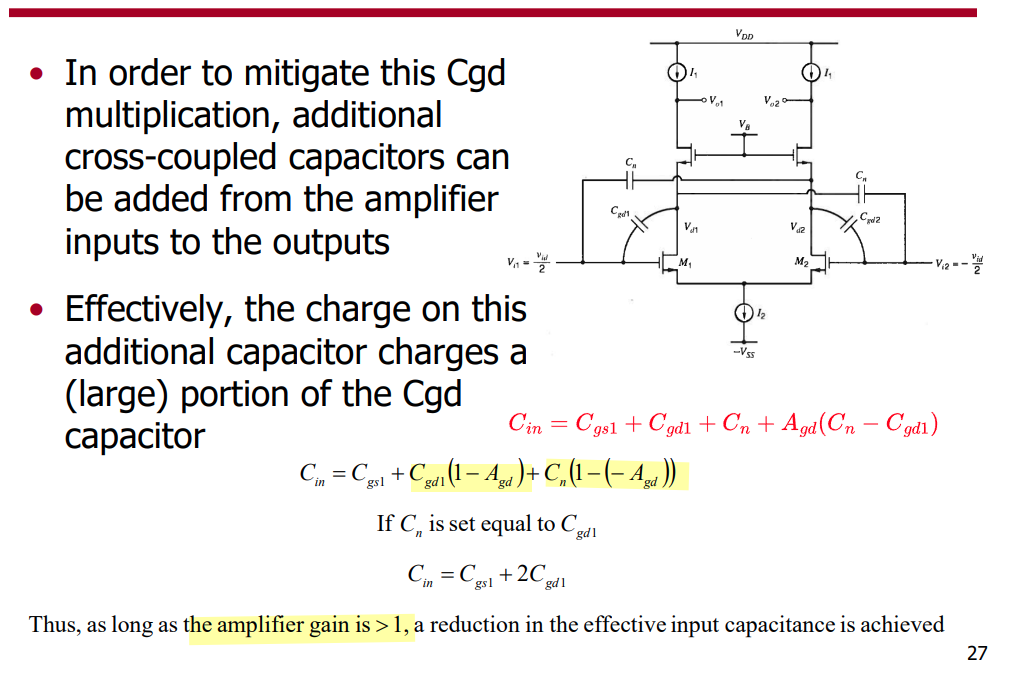
For differential mode input, effective input capacitance \[ C_{in} = C_{gs} +(1+A_{dm}) C_{gd}+\color{red}(1-A_{dm})C_n \] and effective output capacitance \[ C_{out} = C_{dd} + (1+\frac{1}{A_{dm}})C_{gd}+\color{red} (1-\frac{1}{A_{dm}})C_n \] That is \(C_n\) deteriorate the effective output capacitance

For common mode input, effective input capacitance \[ C_{in} = C_{gs} + (1+A_{cm}) C_{gd}+ \color{red}(1+A_{cm})C_n \] and effective output capacitance \[ C_{d1} = C_{dd} + (1+\frac{1}{A_{cm}})C_{gd}+\color{red} (1+\frac{1}{A_{cm}})C_n \] i.e., \(C_n\) deteriorate both effective input capacitance and effective output capacitance, unfortunately


effective input capacitance \(\Pi\) model, which is appropriate for both differential input and common mode input

nmc_pi_in.drawio

Suppose \(C_n=C_{gd}\), effective differential input capacitance is same with effective common-mode input capacitance (\(C_n=\frac{A_{dm}-A_{cm}}{A_{dm}+A_{cm}}C_{gd}\))


XCP with Capacitor

B. Razavi, "The Cross-Coupled Pair - Part III [A Circuit for All Seasons]," IEEE Solid-State Circuits Magazine, Issue. 1, pp. 10-13, Winter 2015. [https://www.seas.ucla.edu/brweb/papers/Journals/BR_Magzine3.pdf]

S. Galal and B. Razavi, "10-Gb/s Limiting Amplifier and Laser/Modulator Driver in 0.18um CMOS Technology,” IEEE Journal of Solid-State Circuits, vol. 38, pp. 2138-2146, Dec. 2003.[https://www.seas.ucla.edu/brweb/papers/Journals/G&RDec03_2.pdf]

A. Sheikholeslami, "Bandwidth Extension [Circuit Intuitions]," in IEEE Solid-State Circuits Magazine, vol. 7, no. 2, pp. 8-11, Spring 2015 [https://www.eecg.utoronto.ca/~ali/papers/mag-spr-15-bandwidth-extention.pdf]

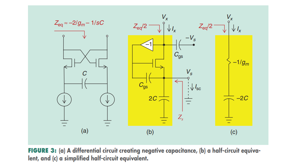
The Cross-Coupled Pair (XCP) can operate as an impedance negator [a.k.a. a negative impedance converter (NIC)]

A common application is to create a negative capacitance that can cancel the positive capacitance seen at a port, thereby improving the speed

image-20240922174319496 \[ I_{NIC} =\frac{V_{im} - V_{ip}}{\frac{2}{g_m}+\frac{1}{sC_c}} = \frac{-2V_{ip}}{\frac{2}{g_m}+\frac{1}{sC_c}} \] Therefore \[ Z_{NIC} = \frac{V_{ip} - V_{im}}{I_{NIC}}=\frac{2V_{ip}}{I_{NIC}} =- \frac{2}{g_m}-\frac{1}{sC_c} \] half-circuit

If \(C_{gd}\) is considered, and apply miller effect. half equivalent circuit is shown as below

nic.drawio


image-20251204223338959

input network

image-20250706110415914


image-20250611075951974

1
2
3
4
5
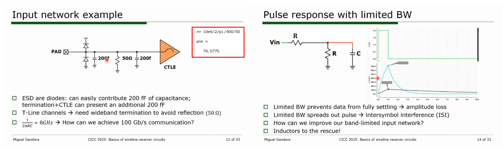
>> 10e6/2/pi/400/50

ans =

79.5775

CTLE transfer function

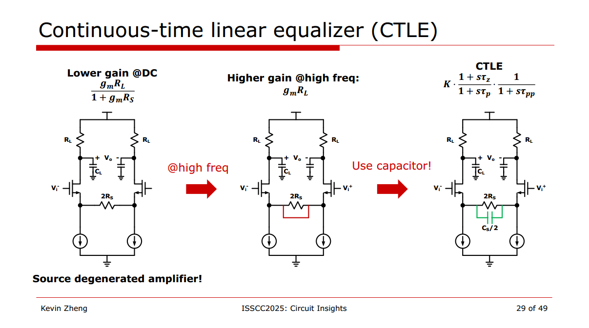
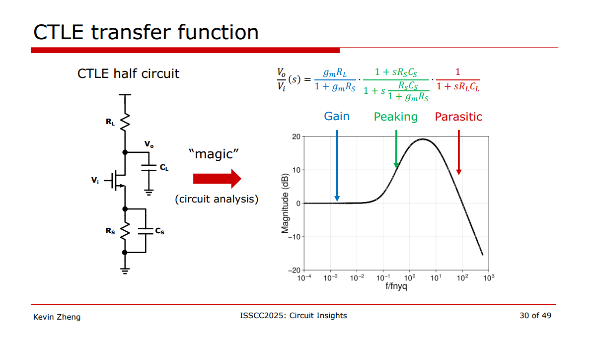
Circuit Insights @ ISSCC2025: Circuits for Wireline Communications - Kevin Zheng [https://youtu.be/8NZl81Dj45M&t=1045]

image-20260328182328792

image-20260328182339762


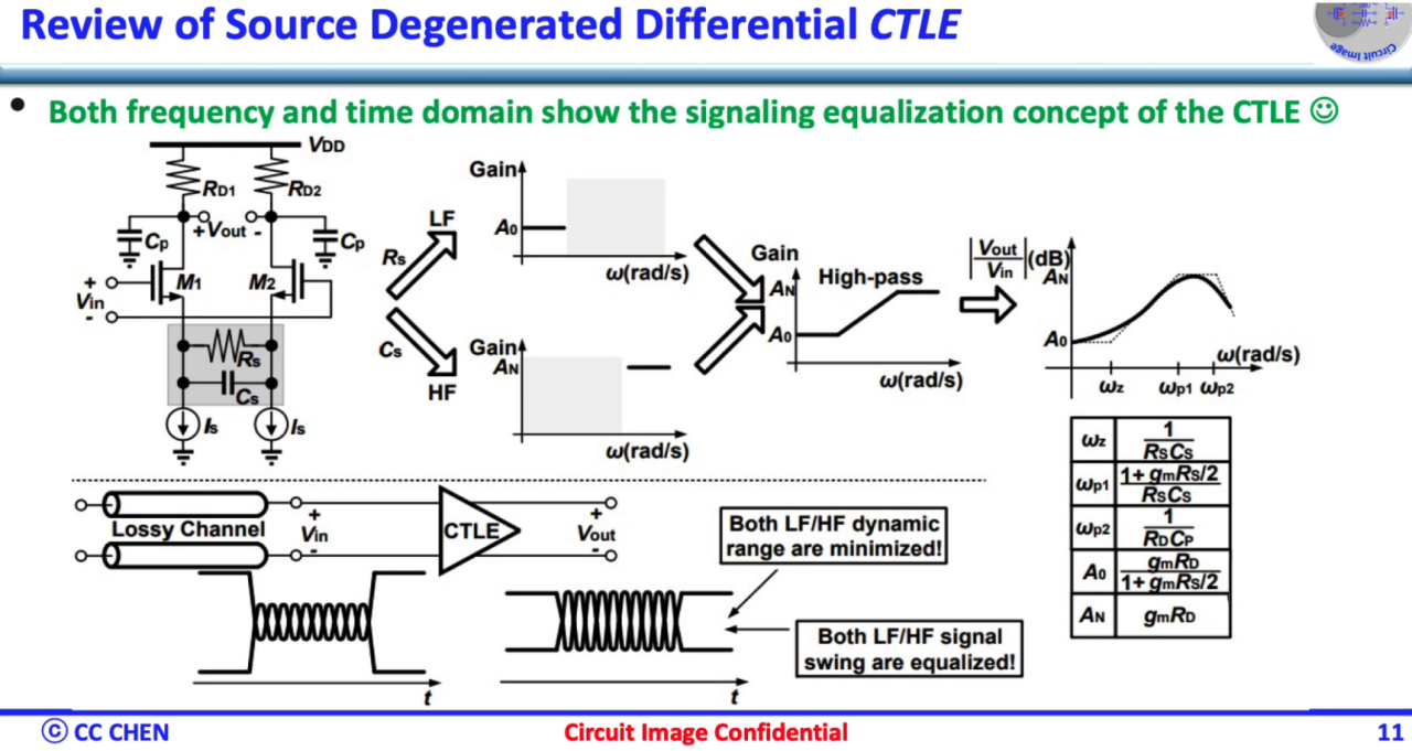
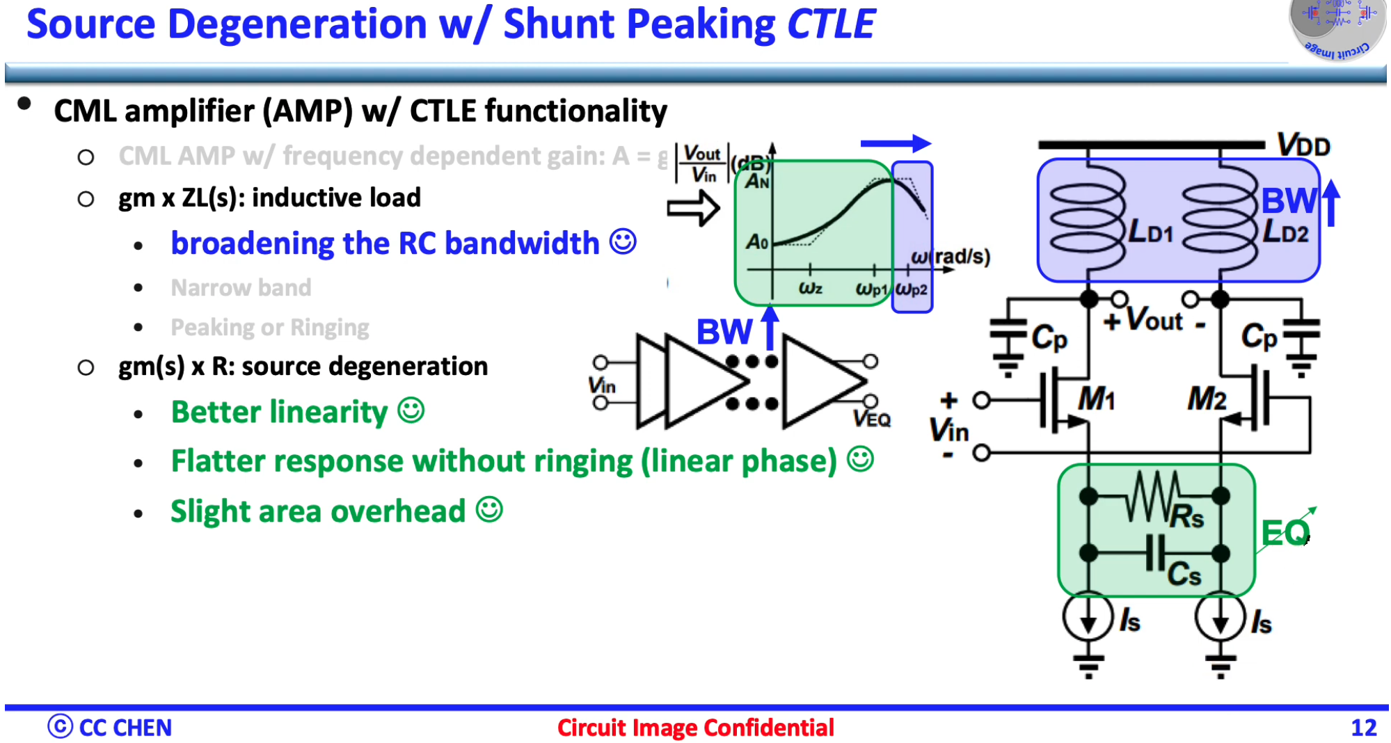
Why Shunt-peaking or Source Degenerated type Active CTLE? [https://youtu.be/EFMZG-FIWeo]

image-20260519232914332

Shunt Peaking broaden the RC bandwidth

image-20260519233200484

image-20260526210821835

image-20260526210739466

Equalization Shaping

PCIe Gen6 Channel and Reference Package S4P Models for Rx Stressed Eye Calibration

image-20251204005909804

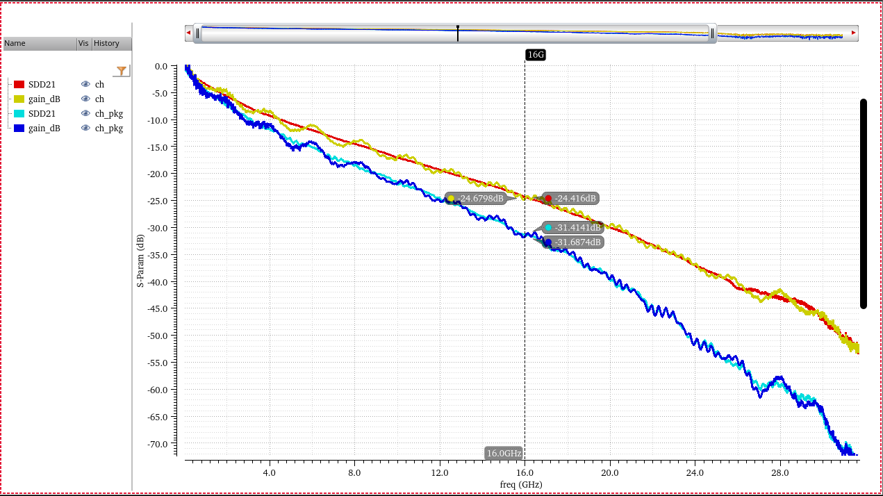
Above curve demonstrate that only zero is not enough to compensate channel+pkg loss (>20 dB/decade), peaking or Complex-Conjugate Poles is necessary

image-20251204005738743


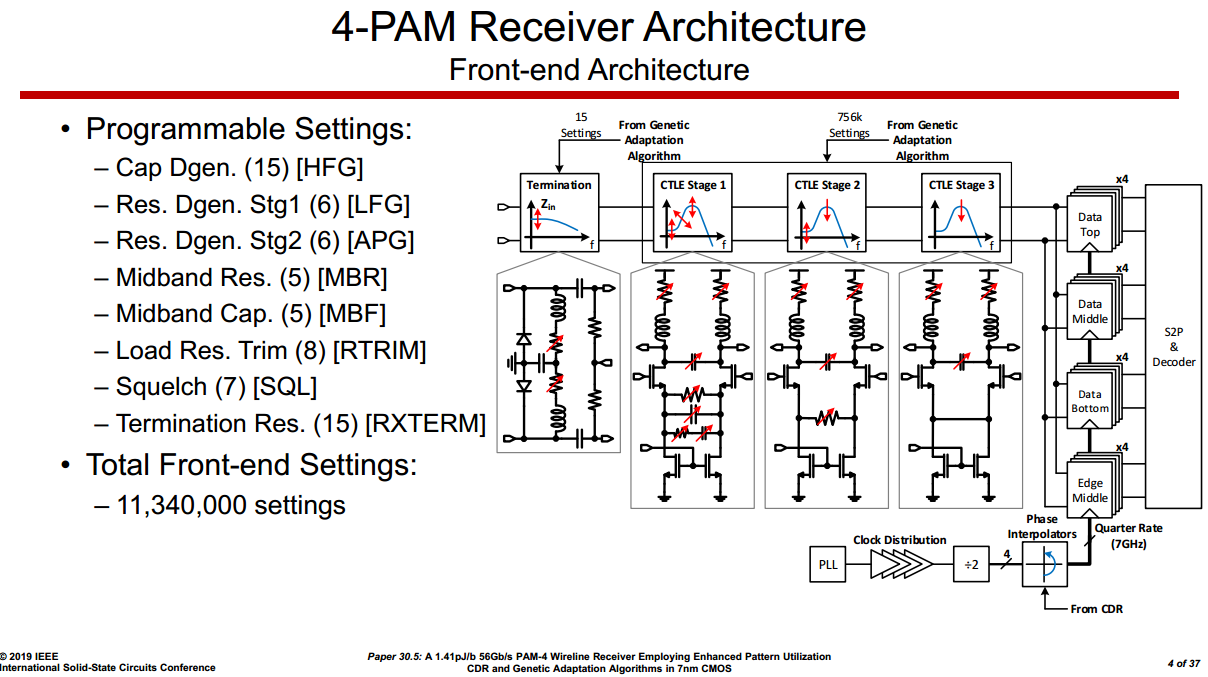
S. Shahramian et al., "30.5 A 1.41pJ/b 56Gb/s PAM-4 Wireline Receiver Employing Enhanced Pattern Utilization CDR and Genetic Adaptation Algorithms in 7nm CMOS," 2019 IEEE International Solid-State Circuits Conference - (ISSCC), San Francisco, CA, USA, 2019 [pdf]

image-20251203231733124


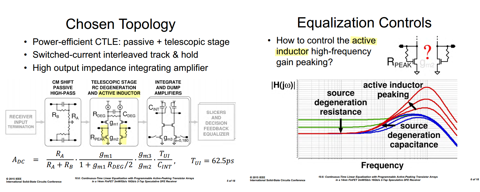
P. A. Francese et al., "10.6 continuous-time linear equalization with programmable active-peaking transistor arrays in a 14nm FinFET 2mW/Gb/s 16Gb/s 2-Tap speculative DFE receiver," 2015 IEEE International Solid-State Circuits Conference - (ISSCC) Digest of Technical Papers, San Francisco, CA, USA, 2015 [pdf]

image-20251203232523501


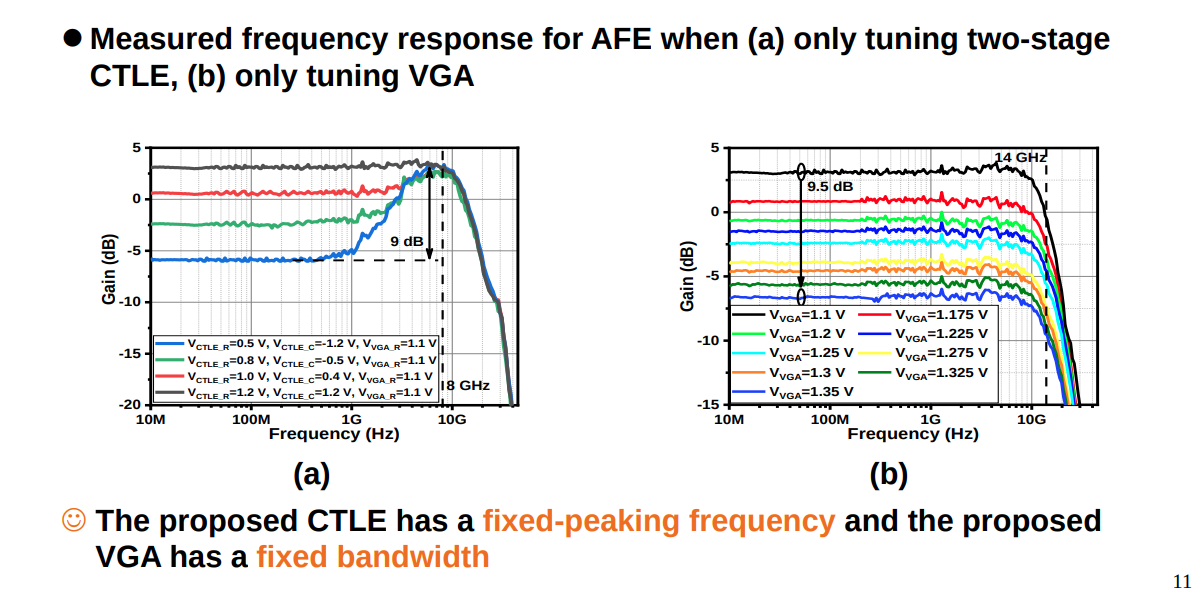
Z. Li, M. Tang, T. Fan and Q. Pan, "A 56-Gb/s PAM4 Receiver Analog Front-End With Fixed Peaking Frequency and Bandwidth in 40-nm CMOS," in IEEE Transactions on Circuits and Systems II: Express Briefs, vol. 68, no. 9, pp. 3058-3062, Sept. 2021 [slides] [paper]

In the active copper cable (ACC) application, it is necessary to give different equalizations at the same frequency according to different cable lengths, Therefore, the AFE with fixed peaking frequency and constant bandwidth is desirable for these applications

image-20251217224711701

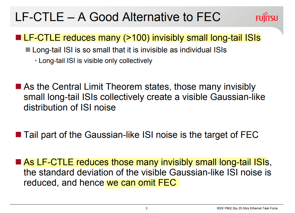
Low-Frequency CTLE (LF-CTLE)

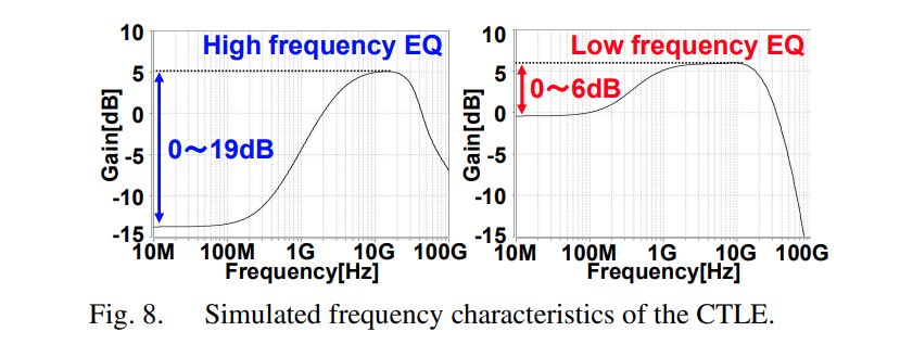
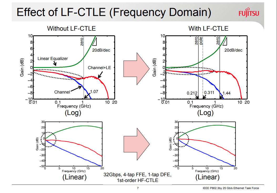
S. Parikh et al., "A 32Gb/s wireline receiver with a low-frequency equalizer, CTLE and 2-tap DFE in 28nm CMOS," 2013 IEEE International Solid-State Circuits Conference Digest of Technical Papers, San Francisco, CA, USA, 2013 [https://sci-hub.se/10.1109/ISSCC.2013.6487622]

T. Shibasaki et al., "A 56-Gb/s receiver front-end with a CTLE and 1-tap DFE in 20-nm CMOS," 2014 Symposium on VLSI Circuits Digest of Technical Papers, Honolulu, HI, USA, 2014, pp. 1-2

Yasuo Hidaka Comment #146, #174: Low-Frequency CTLE to support 3m cable w/o FEC [https://www.ieee802.org/3/by/public/Sept15/hidaka_3by_01_0915.pdf]

image-20251217233444843

image-20251217234434659

image-20251217234637716

Gm-TIA CTLE

H. Kimura et al., "A 28 Gb/s 560 mW Multi-Standard SerDes With Single-Stage Analog Front-End and 14-Tap Decision Feedback Equalizer in 28 nm CMOS," in IEEE Journal of Solid-State Circuits, vol. 49, no. 12, pp. 3091-3103, Dec. 2014 [https://ieeexplore.ieee.org/ielx7/4/6963535/06894632.pdf]

Pisati, et.al., "Sub-250mW 1-to-56Gb/s Continuous-Range PAM-4 42.5dB IL ADC/DAC- Based Transceiver in 7nm FinFET," 2019 IEEE International Solid-State Circuits Conference (ISSCC), 2019 [https://sci-hub.se/10.1109/ISSCC.2019.8662428]

Z. Li, M. Tang, T. Fan and Q. Pan, "A 56-Gb/s PAM4 Receiver Analog Front-End With Fixed Peaking Frequency and Bandwidth in 40-nm CMOS," in IEEE Transactions on Circuits and Systems II: Express Briefs, vol. 68, no. 9, pp. 3058-3062, Sept. 2021 [slides] [paper]

K. Kwon et al., "A 212.5Gb/s Pam-4 Receiver With Mutual Inductive Coupled Gm-Tia in 4nm Finfet," 2025 Symposium on VLSI Technology and Circuits (VLSI Technology and Circuits), Kyoto, Japan, 2025

Bae, W. (2019). CMOS Inverter as Analog Circuit: An Overview. Journal of Low Power Electronics and Applications. [pdf]

CTLE, with Gm + TIA structure

image-20250904202636824


Chongyun ZHANG, 2025, "Energy-Efficient CMOS Optical Receiver for Short-Reach Data Center Application,". [slides, paper]

image-20251202222813043

image-20251202222831594

Equalization Noise Enhancement

Advanced Signal Integrity for High-Speed Digital Designs, S. H. Hall and H. L. Heck, John Wiley & Sons, 2009

CC Chen, Why CTLE? [https://youtu.be/zsuJMqadaKY]

image-20251021211402274

image-20250904235434247

Assuming \(\mathrm{SNR}(f) = \frac{S_x(f)}{S_n(f)}\)


trade-offs between noise amplification and signal equalization

dual-diode based ESD protection

image-20260801014821774

??? which diodes are used in right topology — both pdiode and ndiode are used


image-20260801022107783

CTLE paper

J. Im et al., "A 112-Gb/s PAM-4 Long-Reach Wireline Transceiver Using a 36-Way Time-Interleaved SAR ADC and Inverter-Based RX Analog Front-End in 7-nm FinFET," in IEEE Journal of Solid-State Circuits, vol. 56, no. 1, pp. 7-18, Jan. 2021, doi: 10.1109/JSSC.2020.3024261

A. Khairi et al., "A 1.41-pJ/b 224-Gb/s PAM4 6-bit ADC-Based SerDes Receiver With Hybrid AFE Capable of Supporting Long Reach Channels," in IEEE Journal of Solid-State Circuits, vol. 58, no. 1, pp. 8-18, Jan. 2023, doi: 10.1109/JSSC.2022.3211475

D. Pfaff et al., "A 224 Gb/s 3 pJ/bit 40 dB Insertion Loss Transceiver in 3-nm FinFET CMOS," in IEEE Journal of Solid-State Circuits, vol. 60, no. 1, pp. 9-22, Jan. 2025, doi: 10.1109/JSSC.2024.3466092

reference

J. Kim et al., "A 112Gb/s PAM-4 transmitter with 3-Tap FFE in 10nm CMOS," 2018 IEEE International Solid-State Circuits Conference - (ISSCC), San Francisco, CA, USA, 2018 [paper] [slides]

Miguel Gandara. CICC2025 Circuits Insights: Wireline Receiver Circuits [https://youtu.be/X4JTuh2Gdzg]

Elad Alon, ISSCC 2014, "T6: Analog Front-End Design for Gb/s Wireline Receivers"

Byungsub Kim, ISSCC 2022, "T11: Basics of Equalization Techniques: Channels, Equalization, and Circuits"

Gain Kim, 2023. Equalization, Architecture, and Circuit Design for High-Speed Serial Link Receiver [https://www.theise.org/wp-content/uploads/2023/10/Analog_1_%EA%B9%80%EA%B0%80%EC%9D%B8%EA%B5%90%EC%88%98%EB%8B%98_DGIST_LectureNote-Min-Jae-Seo.pdf]


S. Shekhar, J. S. Walling and D. J. Allstot, "Bandwidth Extension Techniques for CMOS Amplifiers," in IEEE Journal of Solid-State Circuits, vol. 41, no. 11, pp. 2424-2439, Nov. 2006 [pdf]

David J. Allstot Bandwidth Extension Techniques for CMOS Amplifiers [https://ewh.ieee.org/r5/denver/sscs/Presentations/2007_08_Allstot.pdf]

S. S. Mohan, M. D. M. Hershenson, S. P. Boyd and T. H. Lee, "Bandwidth extension in CMOS with optimized on-chip inductors," in IEEE Journal of Solid-State Circuits, vol. 35, no. 3, pp. 346-355, March 2000 [http://smirc.stanford.edu/papers/JSSC00MAR-mohan.pdf]

J. Paramesh and D. J. Allstot, "Analysis of the Bridged T-Coil Circuit Using the Extra-Element Theorem," in IEEE Transactions on Circuits and Systems II: Express Briefs, vol. 53, no. 12, pp. 1408-1412, Dec. 2006 [https://sci-hub.st/10.1109/TCSII.2006.885971]

S. C. D. Roy, "Comments on "Analysis of the Bridged T-coil Circuit Using the Extra-Element Theorem," in IEEE Transactions on Circuits and Systems II: Express Briefs, vol. 54, no. 8, pp. 673-674, Aug. 2007 [https://sci-hub.st/10.1109/TCSII.2007.899834]

B. Razavi, "The Bridged T-Coil [A Circuit for All Seasons]," IEEE Solid-State Circuits Magazine, Volume. 7, Issue. 40, pp. 10-13, Fall 2015 [https://www.seas.ucla.edu/brweb/papers/Journals/BRFall15TCoil.pdf]

—, "The Design of Broadband I/O Circuits [The Analog Mind]," IEEE Solid-State Circuits Magazine, Volume. 13, Issue. 2, pp. 6-15, Spring 2021 [http://www.seas.ucla.edu/brweb/papers/Journals/BR_SSCM_2_2021.pdf]

Deog-Kyoon Jeong. Topics in IC Design: T-Coil [pdf]

P. Heydari, "Neutralization Techniques for High-Frequency Amplifiers: An Overview," in IEEE Solid-State Circuits Magazine, vol. 9, no. 4, pp. 82-89, Fall 2017 [https://sci-hub.ru/10.1109/MSSC.2017.2745858]

—, "Evolution of Broadband Amplifier Design: From Single-Stage to Distributed Topology," in IEEE Microwave Magazine, vol. 24, no. 9, pp. 18-29, Sept. 2023

Cowan G. Mixed-Signal CMOS for Wireline Communication: Transistor-Level and System-Level Design Considerations. Cambridge University Press; 2024

Starič, Peter and Erik Margan. Wideband amplifiers. (2006) [pdf]

Bob Ross. IBIS Summit [T-Coils and Bridged-T Networks], [T-Coil Topics]

Walling, Jeffrey & Shekhar, Sudip & Allstot, David. (2008). Wideband CMOS Amplifier Design: Time-Domain Considerations. Circuits and Systems I: Regular Papers, IEEE Transactions on. 55. 1781 - 1793. [pdf]

A. A. Abidi, "The T-Coil Circuit Demystified," in IEEE Transactions on Circuits and Systems I: Regular Papers, vol. 72, no. 9, pp. 4469-4480, Sept. 2025

S. Lin, D. Huang and S. Wong, "Pi Coil: A New Element for Bandwidth Extension," in IEEE Transactions on Circuits and Systems II: Express Briefs, vol. 56, no. 6, pp. 454-458, June 2009

M. Kossel et al., "A T-Coil-Enhanced 8.5 Gb/s High-Swing SST Transmitter in 65 nm Bulk CMOS With <−16 dB Return Loss Over 10 GHz Bandwidth," in IEEE Journal of Solid-State Circuits, vol. 43, no. 12, pp. 2905-2920, Dec. 2008 [https://web.mit.edu/magic/Public/papers/04684644.pdf]


S. Galal and B. Razavi, "Broadband ESD protection circuits in CMOS technology," in IEEE Journal of Solid-State Circuits, vol. 38, no. 12, pp. 2334-2340, Dec. 2003, [https://sci-hub.jp/10.1109/JSSC.2003.818568]

M. Ker and Y. Hsiao, "On-Chip ESD Protection Strategies for RF Circuits in CMOS Technology," 2006 8th International Conference on Solid-State and Integrated Circuit Technology Proceedings, 2006, pp. 1680-1683 [https://sci-hub.jp/10.1109/ICSICT.2006.306371]

M. Ker, C. Lin and Y. Hsiao, "Overview on ESD Protection Designs of Low-Parasitic Capacitance for RF ICs in CMOS Technologies," in IEEE Transactions on Device and Materials Reliability, vol. 11, no. 2, pp. 207-218, June 2011 [https://sci-hub.jp/10.1109/TDMR.2011.2106129]

Kosnac, Stefan (2021) Analysis of On-Chip Inductors and Arithmetic Circuits in the Context of High Performance Computing [https://archiv.ub.uni-heidelberg.de/volltextserver/30559/1/Dissertation_Stefan_Kosnac.pdf]

Chapter 4.5. High Frequency Passive Devices [https://www.cambridge.org/il/files/7713/6698/2369/HFIC_chapter_4_passives.pdf]


K. Yadav, P. -H. Hsieh and A. Chan Carusone, "Linearity Analysis of Source-Degenerated Differential Pairs for Wireline Applications," in IEEE Open Journal of Circuits and Systems [https://ieeexplore.ieee.org/stamp/stamp.jsp?tp=&arnumber=10769573]

Minsoo Choi et al., "An Approximate Closed-Form Channel Model for Diverse Interconnect Applications," IEEE Transactions on Circuits and Systems-I: Regular Papers, vol. 61, no. 10, pp. 3034-3043, Oct. 2014. [https://sci-hub.jp/10.1109/TCSI.2014.2327275]

A resonant circuit refers to an electrical circuit using circuit elements such as an inductor (L) and a capacitor (C) to cause resonance at a specific frequency.

There are two types of resonant circuits:

  • series resonant circuits
  • parallel resonant circuits

In a series resonant circuit, the impedance of the circuit reaches its minimum value at resonance, whereas in a parallel resonant circuit, the impedance reaches its maximum value

image-20251027213420942


image-20260108233832631

antiresonance

image-20260108234008061

Resonant Frequency

\(\zeta \lt 1\): Complex-Conjugate Poles, but not resonant peak

\(\zeta \lt \sqrt{2}/2\): resonant peak

image-20251205220247644

[https://lpsa.swarthmore.edu/Bode/underdamped/underdampedApprox.html]

image-20251205233053573


Prof. M. Green / U.C. Irvine EECS 270C / Winter 2016 Week5 [pdf]

image-20260528002429825

image-20260528003301835

with \(L' = \frac{L}{1 - CR_s^2/L}\)

resonant frequency in right equivalent circuit \[ \omega_r^2 = \frac{1}{L'C} = \frac{1}{LC} - \left(\frac{R_s}{L}\right)^2 \] which shows that the equivalent circuit preserves the resonant frequency of the original network.

image-20260528001727247

LC Resonator

image-20240826223955851

Complex Conjugate Zeros

image-20240826224132736

Complex Conjugate Poles

\(\zeta \to 0\) push \(|G(s)\approx \frac{1}{2\zeta} \to+\infty\)

image-20251027212546424

image-20240826224317197


image-20240826224651954

image-20240826224823886

Frequency selectivity

EEE 211 ANALOG ELECTRONICS [https://www.ee.bilkent.edu.tr/~eee211/LectureNotes/Chapter%20-%2004.pdf]

Parallel resonance

image-20251213165220671

assuming \(i(t) = I_p\cos\omega_0 t\), where \(\omega_0 =1/\sqrt{LC}\) , suppose all current flow into \(R\) \[ V(t) = I_pR\cdot \cos\omega_0 t \] \(I_C\), the current flow through \(C\) \[ \color{red}I_C(t)=C\frac{\mathrm{d}V(t)}{\mathrm{d}t}=-C\omega_0\cdot I_pR\cdot \sin\omega_0 t \] Then, we have voltage between \(L\), given \(I_L = -I_C\) \[ V_L(t) = L\frac{\mathrm{d}I_L(t)}{\mathrm{d}t} = LC\omega_0^2\cdot I_pR\cdot \cos\omega_0 t = I_pR\cdot \cos\omega_0 t \]

Series resonance

image-20251213165337258

assuming \(V(t)=V_s\cos\omega_0t\), where \(\omega_0 =1/\sqrt{LC}\) , suppose all current flow into \(V_C+V_L=0\) \[ V_R(t) = V(t) = V_s\cos\omega_0t \] then \[ I_s(t) = \frac{V_s}{R}\cos\omega_0 t \] \(V_L(t)\) is obtained \[ V_L(t) = L\frac{\mathrm{d}I_s(t)}{\mathrm{d}t} = -L\omega_0\cdot \frac{V_s}{R}\sin\omega_0 t \] Then \[ V_C(t) = V(t) - (V_L(t) + V_R(t)) = -V_L(t) \] Therefore, \(I_C\) current flow through \(C\) \[ I_C(t) = C\frac{\mathrm{d}V_C(t)}{\mathrm{d}t}= LC\omega_0^2\cdot \frac{V_s}{R}\cos\omega_0 t= \frac{V_s}{R}\cos\omega_0 t \] voltage potential between \(L\) and \(C\) \[ \color{red}V_m(t) = V_R(t) + V_L(t) = V_s\cos\omega_0t -L\omega_0\cdot \frac{V_s}{R}\sin\omega_0 t = V_s\sqrt{1+L/R^2C}\cos(\omega_0t+\phi) \] image-20251213180419366

Bandwidth

Frequency response: Resonance, Bandwidth, Q factor [https://ocw.mit.edu/courses/6-071j-introduction-to-electronics-signals-and-measurement-spring-2006/5bcec4bfba5f2e99754b77509e9e7ab4_resonance_qfactr.pdf]

image-20260617004026875

image-20260617003852339

Non ideal capacitor & inductor

Tank Circuits/Impedances [https://stanford.edu/class/ee133/handouts/lecturenotes/lecture5_tank.pdf]

Resonant Circuits [https://web.ece.ucsb.edu/~long/ece145b/Resonators.pdf]

Series & Parallel Impedance Parameters and Equivalent Circuits [https://assets.testequity.com/te1/Documents/pdf/series-parallel-impedance-parameters-an.pdf]

ES Lecture 35: Non ideal capacitor, Capacitor Q and series RC to parallel RC conversion [https://youtu.be/CJ_2U5pEB4o]

Non ideal Capacitor

image-20231224163730529


image-20251009211423154

\[ Q_s = \frac{X_s}{R_s} = X_p\frac{Q_p^2}{Q_p^2+1}\cdot \frac{Q_p^2+1}{R_p} =\frac{Q_p^2}{R_p/X_p}=Q_p \]

So long as \(Q_s\gg 1\) \[ \boxed{R_p \approx Q_s^2R_s \qquad C_p \approx C_s} \]

image-20260619145726643


image-20251011224853381

image-20240119001309410

Non ideal Inductor

image-20231224163740411

So long as \(Q_s\gg 1\) \[ \boxed{R_p \approx Q_s^2R_s \qquad L_p \approx L_s} \]

Q by general definition

RFInsights, Series to Parallel Conversion using Quality Factor [https://www.rfinsights.com/concepts/series-to-parallel/]

image-20260619150655292

Parallel C, R: \[ Q=2\pi\cdot \frac{\frac{1}{2}CV_0^2}{\frac{V_0^2}{2R}\cdot \frac{2\pi}{\omega}}=R\cdot \omega C \]

Series C, R: \[ Q = 2\pi \cdot \left. \frac{\frac{1}{2}CV_0^2}{\frac{I_0^2}{2}R\cdot \frac{2\pi}{\omega}} \right|_{I_0=\omega CV_0} = \frac{1}{R\cdot\omega C} \]

image-20260619161140199

Series L, R: \[ Q=2\pi\cdot \frac{\frac{1}{2}LI_0^2}{\frac{I_0^2}{2}R\cdot \frac{2\pi}{\omega}}=\frac{\omega L}{R} \]

Parallel L, R: \[ Q = 2\pi \cdot \left. \frac{\frac{1}{2}LI_0^2}{\frac{V_0^2}{2R}R\cdot \frac{2\pi}{\omega}} \right|_{V_0=\omega LI_0} = \frac{R}{\omega L} \]

Series/Parallel RLC tank

Makarov, Sergey & Ludwig, Reinhold & Bitar, Joyce. (2016). Practical Electrical Engineering. 10.1007/978-3-319-21173-2. [pdf]

Series Resonant RLC

The series RLC resonator is a voltage divider, driven by an alternating voltage source \(v_s(t)=V_m\cos\omega t\)

image-20260619163323279


image-20260619164058914

The ideal LC circuit never exists in practice


Resonance Condition & Quality Factor Q

image-20260619172617128

image-20260619172848440


bandwidth \(B\) of the series resonant RLC circuit — half-power bandwidth.

image-20260619174310426

image-20260619174321807

image-20260619174637248

Parallel Resonant RLC

The parallel RLC resonator is a current divider circuit, driven by an alternating current source \(i_s(t)=I_m\cos\omega t\)

image-20260619181019444

image-20260619181038704

Loaded Q

unloaded Q, external Q, loaded Q

image-20260701223025684

SRF (Self-Resonant Frequency)

[Understanding RF Inductor Specifications, https://www.ece.uprm.edu/~rafaelr/inel5325/SupportDocuments/doc671_Selecting_RF_Inductors.pdf]

[RFIC-GPT Wiki, https://wiki.icprophet.net/]

image-20240802210109935

\[ f_\text{SRF} = \frac{1}{2\pi \sqrt{LC}} \] The SRF of an inductor is the frequency at which the parasitic capacitance of the inductor resonates with the ideal inductance of the inductor, resulting in an extremely high impedance. The inductance only acts like an inductor below its SRF

image-20241221092745311

  • For choking applications, chose an inductor whose SRF is at or near the frequency to be attenuated

  • For other applications, the SRF should be at least 10 times higher than the operating frequency

    it is more important to have a relatively flat inductance curve (constant inductance vs. frequency) near the required frequency

RLC inspection

image-20260512003152012

For analyzing RLC circuits, Log-Log is indeed the best choice.

image-20260512003526175

1
2
3
4
5
6
7
8
9
10
11
12
13
14
15
16
17
18
19
20
21
22
23
24
25
26
27
28
29
30
% Parameters
R = 100; L = 0.1; C = 10e-6;
f = logspace(1, 4, 1000); % Frequency range: 10Hz to 10kHz
w = 2 * pi * f;

% Calculations
fr = 1 / (2 * pi * sqrt(L * C)); % Resonant frequency (approx 159.15 Hz)
Z_mag = abs(R + 1j*w*L + 1./(1j*w*C)); % Total Impedance Magnitude

% Plotting setup
plot_funcs = {@plot, @semilogx, @semilogy, @loglog};
titles = {'Linear Plot', 'Semilog-X', 'Semilog-Y', 'Log-Log'};

for i = 1:4
subplot(2,2,i);
plot_funcs{i}(f, Z_mag, 'LineWidth', 1.5);
hold on;

% Vertical line for Resonant Frequency
xline(fr, '--r', sprintf(' f_r = %.2f Hz', fr), ...
'LabelVerticalAlignment', 'bottom', 'LineWidth', 1.2);

% Horizontal line for Minimum Impedance (Z = R)
yline(R, '--g', sprintf(' |Z| = R = %d \\Omega', R), ...
'LabelHorizontalAlignment', 'left', 'LineWidth', 1.2);

title(titles{i});
xlabel('Frequency (Hz)'); ylabel('|Z| (Ohms)');
grid on;
end

reference

Pozar, David M. Microwave Engineering. 4th ed. Wiley, 2012. [pdf]

Hossein Hashemi, RF Circuits, [https://youtu.be/0f3yZMvD2Jg]

Resonant Circuits: Resonant Frequency and Q Factor [https://techweb.rohm.com/product/circuit-design/electric-circuit-design/18332/]

J. Nako, G. Tsirimokou, C. Psychalinos and A. S. Elwakil, "Approximation of First–Order Complex Resonators in the Frequency–Domain," in IEEE Access, vol. 13, pp. 54494-54503, 2025 [pdf]

How to generate complex poles without inductor? [https://a2d2ic.wordpress.com/2020/02/19/basics-on-active-rc-low-pass-filters/]

Visvesh Sathe. Resonant Clock Design for a Power-efficient, High-volume x86 -64 Microprocessor [https://ewh.ieee.org/r5/denver/sscs/Presentations/2012_05_Sathe.pdf]

RFInsights, A Journey from Resonance to Impedance Matching Chp. 1: Origin of Q-Factor The Deadly Beginnings, [https://www.rfinsights.com/concepts/quality-factor/]

image-20260613070841886

Mehmet Soyuer. Monolithic Phase-Locked Loops for Clocking [https://ewh.ieee.org/r5/denver/sscs/Presentations/2009_06_Soyuer.pdf]

image-20260808093448775

PD & PFD

Sam Palermo, ECEN620: Network Theory Broadband Circuit Design Fall 2025 Lecture 4: Phase Detector Circuits [https://people.engr.tamu.edu/spalermo/ecen620/lecture04_ee620_phase_detectors.pdf]

Michael Perrott, 6.976 High Speed Communication Circuits and Systems Lecture 15 Integer-N Frequency Synthesizers [https://rfic.eecs.berkeley.edu/courses/ee242/pdf/perrott_lec15.pdf]

Mehmet Soyuer. Monolithic Phase-Locked Loops for Clocking [https://ewh.ieee.org/r5/denver/sscs/Presentations/2009_06_Soyuer.pdf]

Qasim Chaudhari. What are Cycle Slips and Hangup in Phase Locked Loops? [https://wirelesspi.com/what-are-cycle-slips-and-hangup-in-phase-locked-loops/]

image-20260613083929737

XOR Phase Detector

image-20260613083621395

Tristate PFD

image-20260613083646800

image-20260613083715144

image-20260613085340899

PFD requires periodic edges on both inputs

In a CDR, one input is random NRZ data, and a long run of identical bits has no transitions at all

The PFD's state machine interprets those missing edges as a huge phase/frequency error and pumps the loop away from lock

frequency acquisition

image-20260613095817926

image-20260613101004088

[Gist link]

image-20260613101030913

image-20260613101049573

beat period: \(2\pi\cdot T_{beat,per}\cdot \Delta f = 2\pi \to T_{beat,per}=\frac{1}{\Delta f}\)

PFD Deadzone

Sam Palermo, "Lecture 4: Phase Detector Circuit" [https://people.engr.tamu.edu/spalermo/ecen620/lecture04_ee620_phase_detectors.pdf]

image-20260808091337910

Dead zone induced by incomplete settling of charge-pump currents

This situation can be avoided by adding additional delay to the AND gate in the PFD

image-20241222190011244


D. Turker et al., "A 7.4-to-14GHz PLL with 54fsrms jitter in 16nm FinFET for integrated RF-data-converter SoCs," 2018 IEEE International Solid-State Circuits Conference - (ISSCC), San Francisco, CA, USA, 2018 [[https://sci-hub.ru/10.1109/ISSCC.2018.8310342](

image-20260807235323330

\(\tau\) shall be minimized to reduce noise of CP

PFD/CP Modeling

image-20250807225013850

pfdcp-lmdl.drawio

feedback path delay

Dennis Fischette, First Time, Every Time – Practical Tips for PhaseLocked Loop Design [https://www.delroy.com/PLL_dir/tutorial/PLL_tutorial_slides.pdf]

Amir Amirkhany. ISSCC 2019 "Basics of Clock and Data Recovery Circuits"

PFD ZOH

PFD ZOH half reference cycle delay in Open-Loop PLL Gain

image-20260816080527790

\(\color{red}T_\text{pfd}/2\) term is typically an equivalent delay caused by the sampled-data nature of the PFD/charge-pump

image-20260812212850273

Divider delay

An ideal feedback divider does not introduce propagation delay in phase domain

image-20260814202707911

The feedback divider provides a sampled version of the scaled VCO phase, and the PFD obtains the sampled phase error between that feedback phase and the reference phase

There is no delay between oscillator output phase and feedback divider output phase if C2Q and logic propagation delays are neglected

If the real divider has C2Q delay \(t_{CQ}\), then it becomes approximately \[ \boxed{T_d \approx t_{\mathrm{CQ}} + \frac{T_{\mathrm{pfd}}}{2}} \]

retimer at divider output

Darabi H. Radio Frequency Integrated Circuits and Systems. 2nd ed. Cambridge University Press; 2020.

extra one cycle delay vs reducing accumulated noise from the last DFF retiming DFF

image-20260815214721784

image-20260815221958790


Sam Palermo, ECEN620: Network Theory Broadband Circuit Design Fall 2025 Lecture 8: Divider Circuits [https://people.engr.tamu.edu/spalermo/ecen620/lecture08_ee620_dividers.pdf]

image-20260815221034113


L. Romano, S. Levantino, S. Pellerano, C. Samori and A. Lacaita, "Low jitter design of a 0.35 µm-CMOS frequency divider operating up to 3GHz," Proceedings of the 28th European Solid-State Circuits Conference, Florence, Italy, 2002, pp. 611-614. [https://www.researchgate.net/publication/4158185_Low_jitter_design_of_a_035m-CMOS_frequency_divider_operating_up_to_3GHz]

image-20260902233248487

loop delay effect

image-20260812215429178

Cycle Slipping

Dennis Fischette, Could you explain the cycle-skip phenomenon in PLL performance? [https://www.delroy.com/PLL_dir/FAQ/faq_cycle_slip.txt]

image-20260627101018275

image-20260613085103536

image-20260613085238609

Charge Pump Noise

Cyclostationary Noise (Modulated Noise) [https://raytroop.github.io/2024/04/27/noise/#cyclostationary-noise-modulated-noise]

Sam Palermo, Lecture 3: Phase-Locked Loop Systems [https://people.engr.tamu.edu/spalermo/ecen620/lecture03_ee620_pll_system.pdf]

image-20260212205227455


Saurabh Saxena,Phase Locked Loops: Noise Simulations for CP-PLL Blocks [https://youtu.be/Q1libz-XqRw]

image-20250726183455160


Michael H. Perrott, PLL Design Using the PLL Design Assistant Program. [https://designers-guide.org/forum/Attachments/pll_manual.pdf]

M.H. Perrott, M.D. Trott, C.G. Sodini, "A Modeling Approach for Sigma-Delta Fractional-N Frequency Synthesizers Allowing Straightforward Noise Analysis", JSSC, vol 38, no 8, pp 1028-1038, Aug 2002. [https://www.cppsim.com/Publications/JNL/perrott_jssc02.pdf]

image-20240928013058435

Non-ideal Effects in Charge Pump

Sam Palermo, Lecture 11: Clocking Architectures & PLLs [https://people.engr.tamu.edu/spalermo/ecen689/lecture11_ee720_clocking_arch_plls.pdf]

The periodic signal on VCTRL modulates the VCO, giving rise to deterministic jitter


  • Timing Offsets Between Up and Dn Pulses
  • Mismatch Between Charge-Pump Current Sources
  • Incomplete Settling of Charge-Pump Currents
  • Finite Output Resistance of the Charge Pump

Up/Dn Timing Offset

image-20241222171705612

If Dn pulse arrives \(\Delta T\) after the Up pulse, the steady-state VCTRL will be slightly lower than it would be without the \(\Delta T\) mismatch so as to return the VCO's phase to match the reference clocks.

Vice versa, if If Up pulse arrives \(\Delta T\) after the Dn pulse, the steady-state VCTRL will be slightly higher than without \(\Delta T\) mismatch

Current Sources Mismatch

image-20241222174620713

image-20241222174718564


image-20260426171720182


Young, I.A., Greason, J.K., Wong, K.L.: A PLL Clock Generator with 5 to 110MHz of Lock Range for Microprocessors. IEEE Journal of Solid-State Circuits 27(11), 1599– 1607 (1992) [https://people.engr.tamu.edu/spalermo/ecen620/pll_intel_young_jssc_1992.pdf]

Johnson, M., Hudson, E.: A variable delay line PLL for CPU-coprocessor synchronization. IEEE Journal of Solid-State Circuits 23(10), 1218–1223 (1988) [https://sci-hub.se/10.1109/4.5947]

Sam Palermo, Lecture 5: Charge Pump Circuits, ECEN620: Network Theory Broadband Circuit Design Fall 2024 [https://people.engr.tamu.edu/spalermo/ecen620/lecture05_ee620_charge_pumps.pdf]

D. Turker et al., "A 7.4-to-14GHz PLL with 54fsrms jitter in 16nm FinFET for integrated RF-data-converter SoCs," 2018 IEEE International Solid-State Circuits Conference - (ISSCC), San Francisco, CA, USA, 2018 [https://sci-hub.ru/10.1109/ISSCC.2018.8310342]

charge pump with amplifier

image-20260808005243795

off-state leakage

TODO 📅

Incomplete Settling

TODO 📅

W. Rhee, "Design of high-performance CMOS charge pumps in phase-locked loops," 1999 IEEE International Symposium on Circuits and Systems (ISCAS), Orlando, FL, USA, 1999, pp. 545-548 vol.2 [pdf]

Cowan G. Mixed-Signal CMOS for Wireline Communication: Transistor-Level and System-Level Design Considerations. Cambridge University Press; 2024

2nd loop filter

PI (proportional - integral) Loop Filter

image-20240907123938255

image-20240907124029346

image-20240907124018476

LPF leakage

image-20241222192007824

For the sake of simplicity, \(V_{ctr}\) looks like a rectangular pulse with an amplitude of \(I_{CP}R_1\) and a duty ratio of (\(I_{leak}/I_{CP}\)), whose first coefficient of Fourier series is

image-20241222200514941

where \(I_\text{leak} \ll I_{CP}\) is assumed

Then, the peak frequency deviation \(\Delta f\) \[ \Delta f = a_1 \cdot K_v = 2I_\text{leak}R_1 K_v \] using narrowband FM approximation, we have \[ P_\text{spur} = 20\log\left(\frac{\Delta f}{2f_\text{ref}}\right) = 20\log\left(\frac{I_\text{leak}R_1 K_v}{f_\text{ref}}\right) \]

W. Rhee, "Design of high-performance CMOS charge pumps in phase-locked loops," 1999 IEEE International Symposium on Circuits and Systems (ISCAS), Orlando, FL, USA, 1999, pp. 545-548 vol.2 [pdf]

—. Yu, Z., 2024. Phase-Locked Loops: System Perspectives and Circuit Design Aspects. John Wiley & Sons


image-20241222200158107

[https://lpsa.swarthmore.edu/Fourier/Series/ExFS.html]

PFD/CP Simulation

TODO 📅

PLL Characterization

PLL bandwidth by step stimulus

[How can I experimentally find the bandwidth of my PLL?, https://dsp.stackexchange.com/a/73654/59253]

A step response test is an easy way to determine the bandwidth.

Sum a small step into the control voltage of your oscillator (VCO or NCO), and measure the 90% to 10% fall time of the corrected response at the output of the loop filter as shown in this block diagram

PLL Step Response Test

a first order loop \[ BW = \frac{0.35}{t} \space\space\space\space \text{(first order system)} \] Where \(BW\) is the 3 dB bandwidth in Hz and \(𝑡\)​ is the 10%/90% rise or fall time.

For second order loops with a typical damping factor of 0.7 this relationship is closer to: \[ BW = \frac{0.33}{t}\space\space\space\space \text{(second order system, damping factor = 0.7)} \]

PLL BW and peaking by Clock Recovery Method

Rick Eads Principal Planner, Keysight Technologies, PLL Characterization Techniques for High Precision Measurement

John Calvin, Jitter Transfer Function (JTF) analysis Version 1.0 Presented to IEEE P802.3dj Task Force 11/11/2024 [https://grouper.ieee.org/groups/802/3/dj/public/24_11/calvin_3dj_01_2411.pdf]

Michael Schnecker, Clock Recovery Methods for Jitter Analysis [https://cdn.teledynelecroy.com/files/whitepapers/wp_clock_recovery.pdf]

—, DesignCon 2009 Jitter Transfer Measurement in Clock Circuits [https://cdn.teledynelecroy.com/files/whitepapers/designcon2009_lecroy_jitter_transfer_measurement_in_clock_circuits.pdf]

N1076B/7A/7B/8A DCA-M Optical and electric clock data recovery solutions [https://www.keysight.com/us/en/assets/7018-05291/data-sheets/5992-1620.pdf]
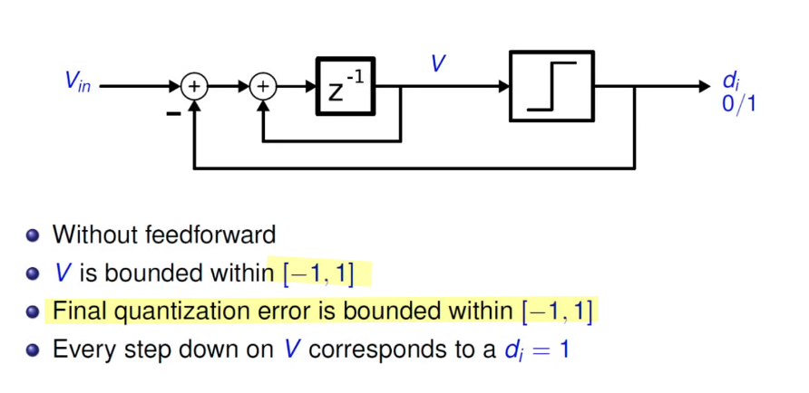
image-20260605235349257

image-20260605234322865

image-20260606003011877


image-20260606115941333

image-20260606120046162

image-20260606120401248

CP-PLL Time domain model

metroidman, fractional N量化噪声对系统相位噪声的影响 两种分析方法 LTI频域法和时域采样DFT法 [link]

classic PLL module transient response

image-20260508211343022

image-20260505162601167

initial state is Reset

image-20260508204250391

classic PLL module in Matlab & Simulink

Kai Wang, Is there a way to improve the code speed? [https://www.mathworks.com/matlabcentral/answers/2039821-is-there-a-way-to-improve-the-code-speed]

classic PLL module in Julia

Julia version (Claude Opus 4.7) [https://gist.github.com/raytroop/53f210b2cca18ec77295dc91dbe35818]

image-20260515202527271

classic PLL module in Mathematica

image-20260507000319278

reference

Lacaita, Andrea Leonardo, Salvatore Levantino, and Carlo Samori. Integrated frequency synthesizers for wireless systems. Cambridge University Press, 2007.

Saurabh Saxena. Noise Simulations for CP-PLL Blocks [https://youtu.be/Q1libz-XqRw]

—, IIT Madras. CICC2022 Clocking for Serial Links - Frequency and Jitter Requirements, Phase-Locked Loops, Clock and Data Recovery

Helene Thibieroz, Customer Support CIC. Using Spectre RF Noise-Aware PLL Methodology to Predict PLL Behavior Accurately [https://citeseerx.ist.psu.edu/document?repid=rep1&type=pdf&doi=3056e59ea76165373f90152f915a829d25dabebc]


Chembiyan T. Chargepump PLL Basics- From A Control Theoretic Viewpoint [linkedin]

—. Challenges in Chargepump PLL Design- A Qualitative Approach [linkedin]

—. A Unified Approach to Low Noise Loop Design in Chargepump PLLs [linkedin]

N. Kuznetsov, A. Matveev, M. Yuldashev and R. Yuldashev, "Nonlinear Analysis of Charge-Pump Phase-Locked Loop: The Hold-In and Pull-In Ranges," in IEEE Transactions on Circuits and Systems I: Regular Papers, vol. 68, no. 10, pp. 4049-4061, Oct. 2021 [https://ieeexplore.ieee.org/stamp/stamp.jsp?arnumber=9509840]


Xiang Gao Credo Semiconductor. ISSCC2018 T1: Low-Jitter PLLs for Wireless Transceivers

Summary of Equalizations

32 to 56 Gbps Serial Link Analysis and Optimization Methods for Pathological Channels [https://docs.keysight.com/eesofapps/files/678068240/678068273/1/1629077956000/tutorial-32-to-56-gbps-serial-link-analysis-optimization-methods-pathological-channels.pdf]
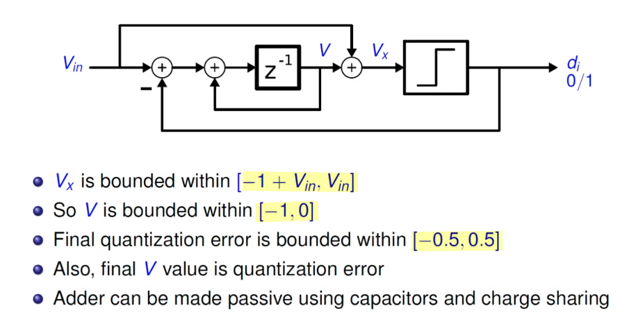
image-20250930160758085

Classification of equalization algorithms

Qasim Chaudhari. A Classification of Equalization Techniques [https://wirelesspi.com/a-classification-of-equalization-techniques/]

image-20260313234954626

CTLE vs. FFE

Keysight Signal Integrity Educational Posts [Post 5: Root Cause of Eye Closure], [Post 6: Eye-opening Experience with CTLE], [Post 7: Eye-opening Experience with FFE]

in the time domain

  • CTLE provide only limited improvement in the pre-cursor ISI, because of the continuous-time, analog nature of CTLE
  • FFE to reduce ISI in both the pre-cursor and post-cursor, because of operating digitally in discrete-time

image-20260227230449898

in the frequency domain

  • CTLE focuses on boosting frequency content at the Nyquist frequency
  • FFE algorithm is selecting taps that effectively amplify the odd harmonics of the Nyquist frequency

image-20260227224843054

In the case of FFE, because of the nature of finite impulse response filter, we would expect amplification and attenuation of different harmonics of Nyquist Frequency


Until 6.5 dB of CTLE DC attenuation, the spread of the single pulse is positive and reaches almost zero at 6.5 dB. As the DC attenuation increases to more than 6.5 dB, the single pulse spectrum is restored too much, resulting in a negative dip at the end of the pulse

image-20260228001551838

the maximum eye opening does not happen at maximum DC attenuation at 9 dB

image-20260228001734379

DFE

Keysight Signal Integrity Educational Posts [Post 8: Eye-opening Experience with DFE]

There are kinks in the eye diagram, the signature of an opened DFE eye is different than other equalizations

DFE algorithm is reducing ISI based on the detected data (symbol)

image-20260228004513829

image-20260228005857811

Since DFE assumes that past symbol decisions are correct. Incorrect decisions from the symbol detector corrupt the filtering of the feedback loop. As a result, the inclusion of the feedforward filter on the front end is crucial in minimizing the probability of error

image-20260427201750201

  • because symbol detection is nonlinear, decision feedback equalization is also nonlinear
  • because of the nonlinearity of the DFE response, it must be modeled in the time domain

FFE vs. DFE

FFE: convolution with input waveform/symbols. Linear.

DFE: convolution with past detected symbols. Recursive and nonlinear because of the slicer.

That is why DFE is not a simple LTI convolution system from input to output.

1
2
3
4
5
received sample r[n] ──┬── subtract ──> slicer ──> detected symbol a_hat[n]
▲ │
│ │
└── DFE filter <─────┘
past decisions

FIR Coefficient Selection

Jose E. Schutt-Aine, Spring 2024 ECE 546 Lecture - 27 Equalization [http://emlab.uiuc.edu/ece546/Lect_27.pdf]
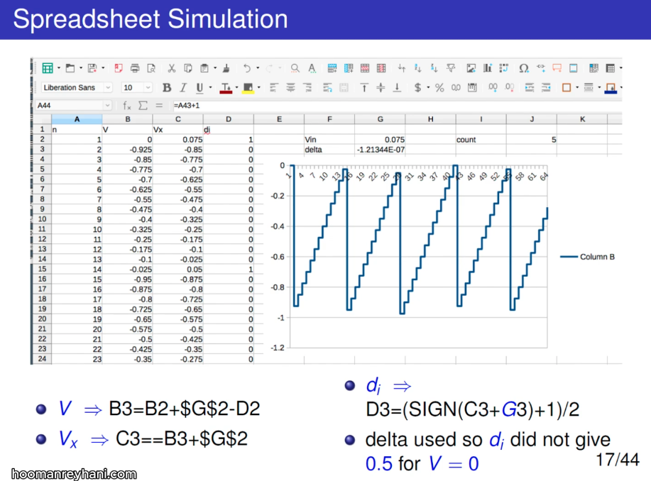
Sam Palermo. Lecture 7 - Equalization Intro & TX FIR EQ [https://people.engr.tamu.edu/spalermo/ecen689/lecture7_ee720_eq_intro_txeq.pdf]
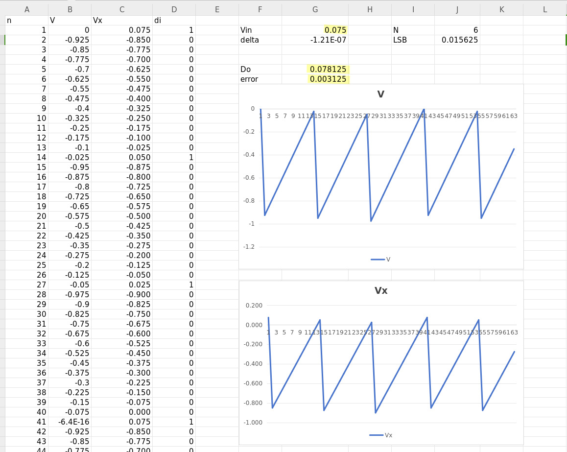
Kevin Zheng, Boris Murmann, Hongtao Zhang, and Geoff Zhang. Feedforward Equalizer Location Study for High-Speed Serial Systems [https://www.signalintegrityjournal.com/articles/1228-feedforward-equalizer-location-study-for-high-speed-serial-systems]

—, "System-Driven Circuit Design for ADC-Based Wireline Data Links", Ph.D. Dissertation, Stanford University, 2018 [https://purl.stanford.edu/hw458fp0168]

Hanumolu, P. K., Wei, G. Y., & Moon, Y. K. (2005). Equalizers for high-speed serial links. International Journal of High Speed Electronics and Systems [https://people.engr.tamu.edu/spalermo/ecen689/hslink_eq_overview_hanumolu_jhses05.pdf]
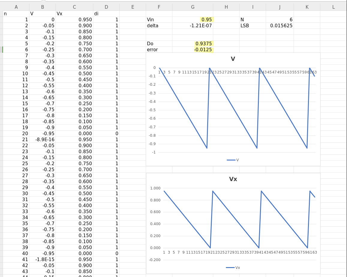
image-20250928235645823

image-20260314000824959

with MMSE

Lecture 7: Equalization Introduction & TX FIR Eq [https://people.engr.tamu.edu/spalermo/ecen689/lecture7_ee720_eq_intro_txeq.pdf]
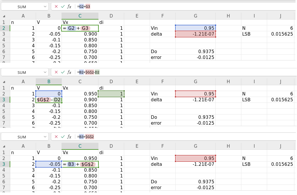
image-20251102114741833

Toeplitz matrix: transforms discrete convolution into \(y=Ax\), where \(x\) is a flattened input vector

tx-ffe-coef-conv.drawio


Lone-Pulse Equalization

image-20251102133644396

tx-ffe-coef-sel.drawio

\[\begin{align} E^TE &=(W^T H^T - Y_{des}^T)(HW-Y_{des})=W^TH^THW+Y_{des}^TY_{des}-W^TH^TY_{des}-Y_{des}^THW \\ &=W^TH^THW+Y_{des}^TY_{des}-2Y_{des}^THW \end{align}\] image-20260116224051584

1
2
3
4
5
6
7
8
9
10
11
12
13
14
15
16
17
18
19
20
21
22
23
24
25
26
27
28
29
30
31
32
33
h=[0.004, 0.0010, 0.0023, 0.0052, 0.0812, 0.3437, 0.1775, 0.0917, 0.0526,...
0.0360, 0.0224, 0.0162, 0.0152, 0.0097, 0.0090, 0.0067];
k = length(h);
n = 3;
l = 1;
m2 = 5;
m1 = 1;

H = zeros([k+n+l-2, n+l-1]);
H(1:end-2,1) = h;
H(2:end-1,2) = h;
H(3:end,3) = h;

Ydes = zeros([k+n+l-2, 1]);
Ydes(m1+m2+1,1) = 1;

HT = transpose(H);

Wls = inv(HT*H)*HT*Ydes;

% Wls =
%
% -0.8177
% 3.7239
% -1.7181

Wlsnorm = Wls/sum(norm(Wls,1));

% Wlsnorm =
%
% -0.1306
% 0.5949
% -0.2745

image-20251102154213244

image-20251102154455603

1
2
3
4
5
6
7
8
9
10
11
12
13
14
15
16
17
18
19
20
21
22
23
24
25
26
fcsvf = readtable("hsample_pre10post20.csv");
h= fcsvf.hsample_Design_Point_1_Y;
k = length(h);
n = 8;
l = 1;
m2 = 10; % channel pre-cursor sample#
m1 = 1;

H = zeros([k+n+l-2, n+l-1]);
for i =1:n
H(i:i+k-1,i) = h;
end

Ydes = zeros([k+n+l-2, 1]);
Ydes(m1+m2+1,1) = 1;

HT = transpose(H);
Wls = inv(HT*H)*HT*Ydes;


Wlsnorm = Wls/sum(norm(Wls,1));
% Wlsnorm =
%
% -0.0926
% 0.6383
% -0.2691

with ZFS

Zero Forcing Solution (ZFS)

image-20260208123317710

image-20260208123432755

\(k=-\text{npre}\) \(k=0\); \(y_\text{target}=1\) \(k=\text{npost}\)
\(c_{-\text{npre}}\) \(x_0\) 0
\(c_{-\text{npre}+1}\) \(x_{-1}\) 0
... ... ... ...
\(c_0\) \(x_{-\text{npre}}\) \(x_0\) \(x_{\text{npost}}\)
... ... ... ...
\(c_{\text{npost}-1}\) \(0\) \(x_1\)
\(c_{\text{npost}}\) \(0\) \(x_0\)

image-20260208122312410


The number of channel samples may exceed the number of equalizer taps to accurately compute the optimal tap coefficients

image-20260228011345326

image-20260228014012124

1
2
3
4
5
6
7
8
9
10
11
12
13
14
15
16
17
18
19
20
21
22
23
24
25
26
27
28
29
30
31
32
33
ht = [0.3, 1.0, -0.2, 0.1, 0.0, 0.0];
ytarget = [0;1;0];

x1 = [[1.0 0.3 0.0];
[-0.2 1.0 0.3];
[0.1 -0.2 1.0]]; % better

x2 = [[1.0 0.3 0.0];
[-0.2 1.0 0.3];
[0.0 -0.2 1.0]];

p1 = inv(x1)*ytarget; % -0.2657 0.8857 0.2037
p2 = inv(x2)*ytarget; % -0.2679 0.8929 0.1786

ht_p1 = conv(ht, p1); % p1 better -> x1
ht_p2 = conv(ht, p2);

% ht_p1 =
%
% -0.0797 0 1.0000 0 0.0478 0.0204 0 0
%
% ht_p2 =
%
% -0.0804 0.0000 1.0000 -0.0268 0.0536 0.0179 0 0

subplot(3,1,1)
stem(ht, 'LineWidth', 2); grid on; xlim([0,10])
subplot(3,1,2)
stem(p1, 'LineWidth', 2); hold on; stem(p2, 'LineWidth', 2);
grid on; legend(["p1" "p2"]); xlim([0,10])
subplot(3,1,3)
stem(ht_p1, 'LineWidth', 2); hold on; stem(ht_p2, 'LineWidth', 2)
grid on; legend(["h\_p1" "h\_p2"]); xlim([0,10])

image-20260314001938792

1
2
3
4
5
6
7
8
9
10
11
12
13
14
15
16
17
18
19
20
21
22
23
h = [0.01 -0.02 0.05 -0.1 0.2 1 0.15 -0.15 0.05 -0.02 0.005];
[val, idx] = max(h);

htc = h(idx-2:idx+2)';

H1 = [1 0.2 -0.1 0.05 -0.02;
0.15 1 0.2 -0.1 0.05;
-0.15 0.15 1 0.2 -0.1;
0.05 -0.15 0.15 1 0.2;
-0.02 0.05 -0.15 0.15 1]; % better

H2 = [1 0.2 -0.1 0 0;
0.15 1 0.2 -0.1 0;
-0.15 0.15 1 0.2 -0.1;
0 -0.15 0.15 1 0.2;
0 0 -0.15 0.15 1];


ytgt = zeros(5,1);
ytgt(3) = 1;

heq1 = inv(H1)*ytgt;
heq2 = inv(H2)*ytgt;

image-20260314005217946

ZFS vs MMSE

minimum mean squared error (MMSE)

There are three major MMSE-based algorithms:

  • least mean square (LMS),
  • normalized least mean square (NLMS)
  • recursive least square (RLS)

image-20260302001712288

image-20260226230127894

  • ZFS eliminates the ISI only at the sampling points that correspond to the equalizer taps. The equalized pulse shows ISI in the intervals between the sample points and at sample points outside the equalizer
  • The Minimum Mean-Square Error Linear Equalizer (MMSE-LE) balances ISI reduction and noise enhancement. The MMSE-LE always performs as well as, or better than, the ZFE

LMS (Least-Mean-Square)

image-20260227221735879

image-20260227222430321


Qasim Chaudhari. Least Mean Square (LMS) Equalizer – A Tutorial [https://wirelesspi.com/least-mean-square-lms-equalizer-a-tutorial/]

image-20260302002909317

CC Chen, Why Background EQ Adaptation? [https://youtu.be/l46OesuNfp4]

image-20260302003217588

TX with SS-LMS

V. Stojanovic et al., "Autonomous dual-mode (PAM2/4) serial link transceiver with adaptive equalization and data recovery," IEEE Journal of Solid-State Circuits, vol. 40, no. 4, pp. 1012–1026, Apr. 2005 [https://sci-hub.ru/10.1109/JSSC.2004.842863]

—, "Channel-Limited High-Speed Links: Modeling, Analysis and Design," PhD. Thesis, Stanford University, Sep. 2004. [pdf]

—, US7423454B2. High speed signaling system with adaptive transmit pre-emphasis [pdf]

image-20260303003640574

image-20260303004118430

image-20260313001119286 \[ dLev_{n+1} = dLev_n - \frac{\Delta_{dLev}}{2}\left(\frac{\partial e_n^2}{\partial dLev_n}\right) = dLev_n - \Delta _{dLev} e_n\left(\frac{\partial (dLev_n-y_n)}{\partial dLev_n}\right) = \color{red} dLev_n - \Delta _{dLev} e_n \] note \(e_n = dLev_n-y_n\)


J. T. Stonick, Gu-Yeon Wei, J. L. Sonntag and D. K. Weinlader, "An adaptive PAM-4 5-Gb/s backplane transceiver in 0.25-μm CMOS," in IEEE Journal of Solid-State Circuits, vol. 38, no. 3, pp. 436-443, March 2003, [https://sci-hub.st/10.1109/JSSC.2002.808282]

image-20260316231021263

RX with SS-LMS

E. -H. Chen et al., "Near-Optimal Equalizer and Timing Adaptation for I/O Links Using a BER-Based Metric," in IEEE Journal of Solid-State Circuits, vol. 43, no. 9, pp. 2144-2156, Sept. 2008 [https://sci-hub.ru/10.1109/JSSC.2008.2001871]

Sam Palermo. ECEN720: High-Speed Links Circuits and Systems [Lecture 7 - Equalization Intro & TX FIR EQ], [Lecture 8 - RX FIR, CTLE, DFE, & Adaptive Eq.]

image-20260313002613321


Jinhyung Lee, Design of High-Speed Receiver for Video Interface with Adaptive Equalization; Phd thesis, August 2019. [thesis link]

image-20260312235927742


Kwangho Lee, Design of Receiver with Offset Cancellation of Adaptive Equalizer and Multi-Level Baud-Rate Phase Detector; Phd thesis, August 2021.[pdf]

image-20260312221305468

\(e[n] = d[n] - Dlev_n\cdot tx[n]\)

image-20260312215652390

Bang-Bang CDR

Alexander PD or !!PD

By definition the edge sample will be zero at a zero crossing, given \(a_na_{n+1}=-1\)

image-20260315161503187

image-20260315161701385

By proper equalization choice, the pulse response may approximate even symmetry

image-20260315162345071 \[ f(t) = g(t+T/2) - g(t-T/2) \]

1
2
3
4
5
6
7
8
9
10
11
12
13
14
15
16
17
18
19
20
21
22
23
24
25
26
27
28
29
30
31
# https://share.google/aimode/l0gnYPTxlyUa7WUed

import numpy as np
import matplotlib.pyplot as plt

t = np.linspace(-1.5, 1.5, 1000)

# Pulse Response and its continuous derivative
p = np.exp(-4 * t ** 2)
p_prime = -8 * t * np.exp(-4 * t ** 2)

# Discrete Approximation (Finite Difference over T=1 UI)
T = 1
discrete_approx = (np.exp(-4 * (t + T / 2) ** 2) - np.exp(-4 * (t - T / 2) ** 2)) / T

# Alexander Bang-Bang Output
g_tau = np.sign(discrete_approx)

plt.figure(figsize=(10, 6))
plt.plot(t, p, label="Pulse Response", color='k', alpha=0.8)
plt.plot(t, p_prime, label="Continuous Derivative $P'(t)$", color='red', alpha=0.6)
plt.plot(t, discrete_approx, label="Discrete Finite Difference Approx", color='blue', ls='--')
plt.step(t, g_tau, where='mid', color='green', lw=1, label="Alexander PD Timing Function", alpha=0.6)
plt.axhline(0, color='black', lw=1)
plt.axvline(0, color='gray', ls=':', lw=1, label='Lock Point')
plt.title('Discrete Approximation of Pulse Derivative (Page 42)')
plt.xlabel('Phase Error (UI)')
plt.ylabel('Amplitude')
plt.legend()
plt.grid(True, alpha=0.3)
plt.show()

image-20260315162737717

Alexander (Bang-Bang) PD does not typically lock at the maximum pulse value when the pulse is asymmetric.

For an asymmetric pulse (like one with a slow trailing edge caused by ISI), this lock point shifts toward the slower-decaying side of the pulse.

image-20260315201620989

1
2
3
4
5
6
7
8
9
10
11
12
13
14
15
16
17
18
19
20
21
22
23
24
25
26
27
28
29
# https://share.google/aimode/l0gnYPTxlyUa7WUed

import numpy as np
import matplotlib.pyplot as plt


t = np.linspace(-1, 1.5, 1000)
T = 1 # Sampling width

# Asymmetric Pulse: Fast rise, slow tail
p = 0.8 * np.exp(-15 * (t + 0.1) ** 2) + 0.4 * np.exp(-1.5 * (t - 0.4) ** 2)

# Calculate Slope Approximation (Alexander PD Function)
p_plus = np.interp(t + T / 2, t, p)
p_minus = np.interp(t - T / 2, t, p)
slope = (p_plus - p_minus) / T

# Find Critical Points
t_peak = t[np.argmax(p)]
t_lock = t[np.argmin(np.abs(slope))]

plt.figure(figsize=(10, 5))
plt.plot(t, p, label="Asymmetric Pulse", lw=2)
plt.plot(t, slope, label="Discrete Finite Difference Approx", color='blue', ls='--')
plt.axvline(t_peak, color='red', ls='--', label=f'True Peak: {t_peak:.2f} UI')
plt.axvline(t_lock, color='green', ls='-', label=f'PD Lock Point: {t_lock:.2f} UI')
plt.title("Sampling Error in Alexander PD due to Pulse Asymmetry")
plt.legend(); plt.grid(True, alpha=0.3)
plt.show()

Kwangho Lee, "Design of Receiver with Offset Cancellation of Adaptive Equalizer and Multi-Level Baud-Rate Phase Detector" [https://s-space.snu.ac.kr/bitstream/10371/177584/1/000000167211.pdf]

Shahramian, Shayan, "Adaptive Decision Feedback Equalization With Continuous-time Infinite Impulse Response Filters" [https://tspace.library.utoronto.ca/bitstream/1807/77861/3/Shahramian_Shayan_201606_PhD_thesis.pdf]

MENIN, DAVIDE, "Modelling and Design of High-Speed Wireline Transceivers with Fully-Adaptive Equalization" [https://air.uniud.it/retrieve/e27ce0ca-15f7-055e-e053-6605fe0a7873/Modelling%20and%20Design%20of%20High-Speed%20Wireline%20Transceivers%20with%20Fully-Adaptive%20Equalization.pdf]


Oh, Kyung Suk, and Xingchao Yuan. High Speed Signaling Jitter Modeling, Analysis, and Budgeting. Pearson Education, 2012

image-20260404103850471

Mueller-Muller CDR

Faisal A. Musa. "HIGH-SPEED BAUD-RATE CLOCK RECOVERY" [https://www.eecg.utoronto.ca/~tcc/thesis-musa-final.pdf]

—."CLOCK RECOVERY IN HIGH-SPEED MULTILEVEL SERIAL LINKS" [https://www.eecg.utoronto.ca/~tcc/faisal_iscas03.pdf]
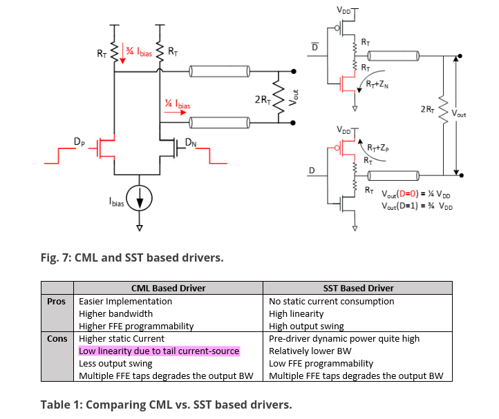
K. Yadav, P. -H. Hsieh and A. C. Carusone, "Loop Dynamics Analysis of PAM-4 Mueller–Muller Clock and Data Recovery System," in IEEE Open Journal of Circuits and Systems, vol. 3, pp. 216-227, 2022 [https://ieeexplore.ieee.org/stamp/stamp.jsp?arnumber=9910561]

Jaeduk Han, "Design and Automatic Generation of 60Gb/s Wireline Transceivers" [https://www2.eecs.berkeley.edu/Pubs/TechRpts/2019/EECS-2019-143.pdf]

S. Kim, K. K. Tokgoz and G. Kim, "Modeling and Simulation of Mueller-Muller Clock Data Recovery System for PAM-4 Wireline Transceivers," 2025 IEEE/IEIE International Conference on Consumer Electronics-Asia (ICCE-Asia), Busan, Korea, Republic of, 2025, pp. 1-3, doi: 10.1109/ICCE-Asia67487.2025.11263607

image-20260316001106973

image-20260316001435496


Mueller-Muller type A timing function

image-20260316000555457

Mueller-Muller type B timing function

image-20260316000723470

image-20260316000303776

1
2
3
4
5
6
7
8
9
10
11
12
13
14
15
16
17
18
19
20
21
22
23
24
25
26
27
28
29
30
31
32
33
34
35
# https://share.google/aimode/ajIRVJNOatjPnY2zp

import numpy as np
import matplotlib.pyplot as plt

# 1. Asymmetric Pulse Modeling
t_cont = np.linspace(-3, 8, 2000)
h_cont = np.where(t_cont >= -0.8, (t_cont + 0.8) * np.exp(-0.6 * (t_cont + 0.8)), 0)
h_cont /= np.max(h_cont)

def get_h(phase):
return np.interp(phase, t_cont, h_cont)

# 2. Timing Error Calculations
phases = np.linspace(-0.5, 3.5, 1000)
tef_a = np.array([get_h(ts + 1) - get_h(ts - 1) for ts in phases])
tef_b = np.array([get_h(ts - 1) for ts in phases])

# 3. Robust Lock Logic
t_lock_a = phases[np.argmin(np.abs(tef_a))]

# Type B: Finding the LAST minimal error before h(-1) rises
indices_b = np.where(np.abs(tef_b) == np.min(np.abs(tef_b)))[0]
t_lock_b = phases[indices_b][-1]

# 4. Plotting Results
plt.figure(figsize=(10, 6))
plt.plot(t_cont, h_cont, 'k-', lw=2, label='Pulse Response $h(t)$')
plt.axvline(t_lock_a, color='red', linestyle='--', label=f'Type A Lock: {t_lock_a:.2f}T')
plt.axvline(t_lock_b, color='green', linestyle='--', label=f'Type B Lock: {t_lock_b:.2f}T')
plt.plot(t_lock_b - 1, get_h(t_lock_b - 1), 'go', label='Type B: $h_{-1}=0$')
plt.title('Baud Rate Lock: Type A (Symmetry) vs. Type B (Last-Zero Precursor)')
plt.legend()
plt.grid(True, alpha=0.3)
plt.show()

image-20240812222307061

Suppose 1-precursor, 1-postcursor — \(y_k = d_{k-1}h_1 + d_k h_0 + d_{k+1}h_{-1}\) \[ \color{red}E[y_k\cdot d_{k-1}] - E[y_k\cdot d_{k+1}] = E[|d_{k-1}|^2h_{1}] - E[|d_{k+1}|^2h_{-1}] =h_1-h_{-1} \] MMPD infers the channel response from baud-rate samples of the received data, the adaptation aligns the sampling clock such that pre-cursor is equal to the post-cursor in the pulse response

image-20260112220639499

note \(E[y_k\cdot d_{k+1}] = E[y_{k-1}\cdot d_{k}] = h_{-1}\)

SS-MMPD

F. Spagna et al., "A 78mW 11.8Gb/s serial link transceiver with adaptive RX equalization and baud-rate CDR in 32nm CMOS," 2010 IEEE International Solid-State Circuits Conference - (ISSCC), San Francisco, CA, USA, 2010, [https://sci-hub.ru/10.1109/ISSCC.2010.5433823]

image-20240808001449664

image-20260112221328785

image-20260320230335447

[https://people.engr.tamu.edu/spalermo/ecen689/lecture12_ee720_cdrs.pdf]

image-20240808001501485

image-20260315215701263

image-20260315215014444

image-20260112225032307

Suppose \(x_k = d_{k-1}h_1 + d_k h_0 + d_{k+1}h_{-1}\) and \(x_{k-1} = d_{k-2}h_1 + d_{k-1} h_0 + d_{k}h_{-1}\) \[ \color{red}E\{z_k\} = \frac{1}{2} E\{|d_{k-1}|^2h_1\} - \frac{1}{2} E\{|d_{k}|^2h_{-1}\} = \frac{1}{2}(h_1 - h_{-1}) \]

Reference Level Choice

Chen, J., Gu, Y., Feng, X., Chi, R., Wu, J., & Chen, Y. (2024). Analysis of Mueller–Muller Clock and Data Recovery Circuits with a Linearized Model. Electronics, 13(21), 4218 [https://www.mdpi.com/2079-9292/13/21/4218]

Liu, Tao & Li, Tiejun & Lv, Fangxu & Liang, Bin & Zheng, Xuqiang & Wang, Heming & Wu, Miaomiao & Lu, Dechao & Zhao, Feng. (2021). Analysis and Modeling of Mueller-Muller Clock and Data Recovery Circuits. Electronics. [10. 1888. 10.3390/electronics10161888.]

Gu, Youzhi & Feng, Xinjie & Chi, Runze & Chen, Yongzhen & Wu, Jiangfeng. (2022). Analysis of Mueller-Muller Clock and Data Recovery Circuits with a Linearized Model. [10.21203/rs.3.rs-1817774/v1]

image-20260317224052868

image-20260320231224829

Adjust Locking Point

Avago Technologies, US8649476B2 Adjusting sampling phase in a baud-rate CDR using timing skew [pdf]

Y. Jung, H. -J. Shin, J. Kim, S. Lee, J. -S. Park and K. Park, "A 28-Gb/s Receiver with Baud-Rate CDR Employing Integrated Pattern-Based Phase Detector Achieving ISI Invariant Phase Locking," 2025 IEEE Asian Solid-State Circuits Conference (A-SSCC), Daejeon, Korea, Republic of, 2025,

R. Dokania et al., "10.5 A 5.9pJ/b 10Gb/s serial link with unequalized MM-CDR in 14nm tri-gate CMOS," 2015 IEEE International Solid-State Circuits Conference - (ISSCC) Digest of Technical Papers, San Francisco, CA, USA, 2015 [https://sci-hub.jp/10.1109/ISSCC.2015.7062987]

H. Zhang, B. Jiao, Y. Liao, and G. Zhang, "A Tutorial on PAM4 Signaling for 56G Serial Link," [DesignCon 2016], [DesignCon 2017]

TODO 📅

image-20260315220455757


Kwangho Lee, "Design of Receiver with Offset Cancellation of Adaptive Equalizer and Multi-Level Baud-Rate Phase Detector" [https://s-space.snu.ac.kr/bitstream/10371/177584/1/000000167211.pdf]

\(h_1\) is necessary

  • without DFE

    SS-MMPD locks at the point (\(h_1=h_{-1}\)​)

  • With a 1-tap DFE

    1-tap adaptive DFE that forces the \(h_1\) to be zero, the SS-MMPD locks wherever the \(h_{-1}\)​ is zero and drifts eventually.

    Consequently, it suffers from a severe multiple-locking problem with an adaptive DFE

image-20260315220208339

Pattern filter

pattern main cursor
011 \(s_{011}=-h_1+h_0+h_{-1}\)
110 \(s_{110}=h_1+h_0-h_{-1}\)
100 \(s_{100}=h_1-h_0-h_{-1}\)
001 \(s_{001}=-h_1-h_0+h_{-1}\)

During adapting, we make

  • \(s_{011}\) & \(s_{110}\) are approaching to each other
  • \(s_{100}\) & \(s_{001}\) are approaching to each other

Then, \(h_{-1}\) and \(h_1\) are same, which is desired

reference

Hall, Stephen H., and Howard L. Heck. Advanced Signal Integrity for High-speed Digital Designs. Wiley : IEEE, 2009 [pdf]

Oh, Kyung, and Xing Yuan. High-Speed Signaling: Jitter Modeling, Analysis, and Budgeting. 1st edition. Prentice Hall, 2011. [pdf]

John M. Cioffi, [Chapter 3 - Equalization], [Chapter 6 - Fundamentals of Synchronization]


David Johns. ECE1392H - Integrated Circuits for Digital Communications - Fall 2001: [Equalization], [Timing Recovery]

B. Kim, "Tutorial: Basics of Equalization Techniques: Channels, Equalization, and Circuits," 2022 IEEE International Solid-State Circuits Conference (ISSCC), San Francisco, CA, USA, 2022

Masum Hossain, ISSCC2023 T11: "Digital Equalization and Timing Recovery Techniques for ADC-DSP-based Highspeed Links" [https://www.nishanchettri.com/isscc-slides/2023%20ISSCC/TUTORIALS/T11.pdf]

—, "LOW POWER DIGITAL EQUALIZATION FOR HIGH SPEED SERDES" [https://www.ieeetoronto.ca/wp-content/uploads/2020/06/SSCS_invited_talk.pdf]

Vivek Telang, 2012, Equalization for High-Speed Serdes: System-level Comparison of Analog and Digital Techniques [https://ewh.ieee.org/r5/denver/sscs/Presentations/2012_08_Telang.pdf]

Gain Kim, 2023. Equalization, Architecture, and Circuit Design for High-Speed Serial Link Receiver [pdf]

—, CICC2022 ES4: Equalization, Architecture, and Circuit Design for High-Speed Serial Link Receiver

S. Laxman, "Equalization algorithms in Millimeter wave communication systems," 2017 IEEE Custom Integrated Circuits Conference (CICC), Austin, TX, USA, 2017 [pdf]

A. Amirkhany, "Basics of Clock and Data Recovery Circuits: Exploring High-Speed Serial Links," in IEEE Solid-State Circuits Magazine, vol. 12, no. 1, pp. 25-38, Winter 2020 [https://sci-hub.jp/10.1109/MSSC.2019.2939342]

—, ISSCC2019 T6: "Basics of Clock and Data Recovery Circuits"

Fulvio Spagna, CICC2018 Clock and Data Recovery Systems [pdf]

Wei-Zen Chen, ISSCC2026. T9: Clocking and CDR Techniques for High-Performance Wireline Transceiver

B. Razavi, "The Design of a Clock and Data Recovery Circuit [The Analog Mind]," in IEEE Solid-State Circuits Magazine, vol. 18, no. 3, pp. 11-116, Summer 2026, doi: 10.1109/MSSC.2026.3706674.


A. A. Bazargani, H. Shakiba and D. A. Johns, "MMSE Equalizer Design Optimization for Wireline SerDes Applications," in IEEE Transactions on Circuits and Systems I: Regular Papers [https://www.eecg.utoronto.ca/~johns/nobots/papers/pdf/2024_bazaragani.pdf]

A. Sharif-Bakhtiar, A. Chan Carusone, "A Methodology for Accurate DFE Characterization," IEEE RFIC Symposium, Philadelphia, Pennsylvania, June 2018. [PDF] [Slides – PDF]

Tony Chan Carusone. High Speed Communications Part 11 – SerDes DSP Interactions [https://youtu.be/YIAwLskuVPc]

—, 2022 Optimization Tools for Future Wireline Transceivers [https://www.ieeetoronto.ca/wp-content/uploads/2022/12/UofT-Future-of-Wireline-Workshop-2022.pdf]

Alphawave IP CEO. How DSP is Killing the Analog in SerDes [https://youtu.be/OY2Dn4EDPiA]


S. Kiran, S. Cai, Y. Zhu, S. Hoyos and S. Palermo, "Digital Equalization With ADC-Based Receivers: Two Important Roles Played by Digital Signal Processingin Designing Analog-to-Digital-Converter-Based Wireline Communication Receivers," in IEEE Microwave Magazine, vol. 20, no. 5, pp. 62-79, May 2019 [https://sci-hub.se/10.1109/MMM.2019.2898025]

K. K. Parhi, "Design of multigigabit multiplexer-loop-based decision feedback equalizers," in IEEE Transactions on Very Large Scale Integration (VLSI) Systems, vol. 13, no. 4, pp. 489-493, April 2005 [http://sci-hub.se/10.1109/TVLSI.2004.842935]

T. Toifl et al., "A 3.5pJ/bit 8-tap-feed-forward 8-tap-decision feedback digital equalizer for 16Gb/s I/Os," ESSCIRC 2014 - 40th European Solid State Circuits Conference (ESSCIRC), Venice Lido, Italy, 2014 [https://sci-hub.se/10.1109/ESSCIRC.2014.6942120]


Daniel Friedman, 2018 Considerations and Implementations for High data Rate Serial Link Design [https://www.ieeetoronto.ca/wp-content/uploads/2020/06/DL-Toronto-Nov-2018.pdf]

Hongtao Zhang, DesignCon 2016. PAM4 Signaling for 56G Serial Link Applications − A Tutorial [https://www.xilinx.com/publications/events/designcon/2016/slides-pam4signalingfor56gserial-zhang-designcon.pdf]


Tony Chan Carusone Integrated Systems Laboratory, University of Toronto [https://isl.utoronto.ca/publications/]

Tony Chan Carusone 2022. Optimization Tools for Future Wireline Transceivers [https://www.ieeetoronto.ca/wp-content/uploads/2022/12/UofT-Future-of-Wireline-Workshop-2022.pdf]

Aleksey Tyshchenko, SeriaLink Systems Clinton Walker, Alphawave IP. DesignCon 2022. IBIS-AMI Modeling and Correlation Methodology for ADC-Based SerDes Beyond 100 Gb/s [https://static1.squarespace.com/static/5fb343ad64be791dab79a44f/t/63d807441bcd266de258b975/1675102025481/SLIDES_Track02_IBIS_AMI_Modeling_and_Correlation_Tyshchenko.pdf]

[https://ibis.org/summits/apr22/tyshchenko.pdf]

[https://www.mathworks.com/content/dam/mathworks/conference-or-academic-paper/ibis-ami-modeling-and-correlation.pdf]


Ali Sheikholeslami Electronics Group, University of Toronto [https://www.eecg.utoronto.ca/~ali/]

J. Liang, A. Sheikholeslami, H. Tamura, Y. Ogata and H. Yamaguchi, "Loop Gain Adaptation for Optimum Jitter Tolerance in Digital CDRs," in IEEE Journal of Solid-State Circuits, vol. 53, no. 9, pp. 2696-2708, Sept. 2018 [https://sci-hub.jp/10.1109/JSSC.2018.2839038]

0%