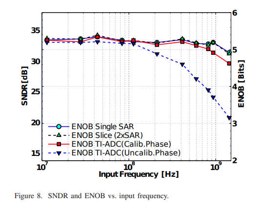
J. Zhong, Y. Zhu, S. -W. Sin, S. -P. U and R. P. Martins, "Thermal
and Reference Noise Analysis of Time-Interleaving SAR and
Partial-Interleaving Pipelined-SAR ADCs," in IEEE Transactions on
Circuits and Systems I: Regular Papers, vol. 62, no. 9, pp. 2196-2206,
Sept. 2015 [https://sci-hub.st/10.1109/TCSI.2015.2452331]
sweep the setup time between ideal pulse input and clock, sample the
output of SFE at falling edge
sample-by-sample
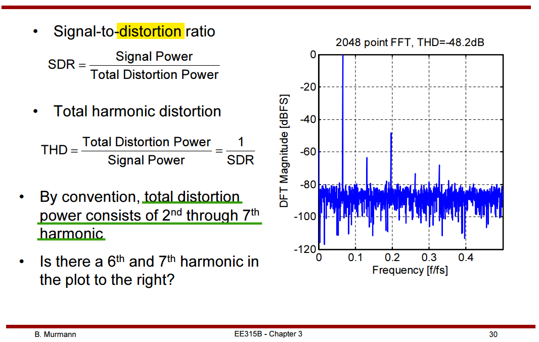
3rd harmonic
bit-by-bit
The amplitude of the reference ripple is code-dependent as it is
correlated with switching energy in each bit cycling
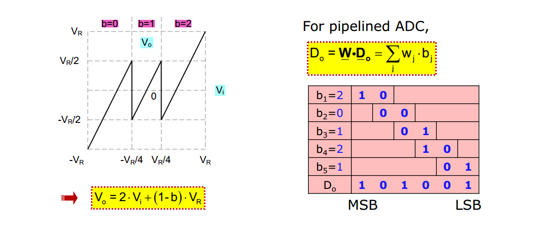
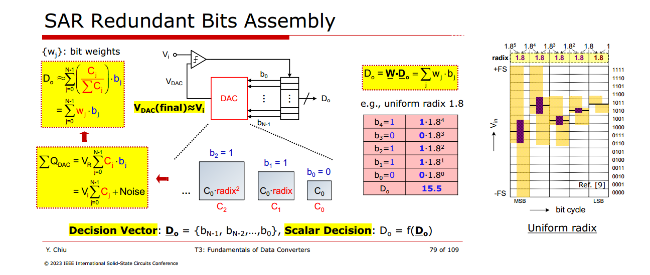
Redundancy
decision level
final digital output for an \(N\)-bit \(M\)-step ADC can be calculated \[
D_{out} = s(M) + \sum_{i=1}^{M-1}(2\cdot b[i] - 1)\times s(i) + (b[0]
-1)\cdot s(1)
\]
i
M
M-1
M-2
...
2
1
0
b[i]
b[M-1]
b[M-2]
...
b[2]
b[1]
b[0]
s[i]
s(M)
s(M-1)
s(M-2)
...
s(2)
s(1)
track the decision level
For \(N\)-bit binary weighted
algorithm,\(N=M\) and \(s(i)=2^{i-1}\), where \(i\in \{N, N-1,...,2,1 \}\)
For the \(n\)th output bit, once a
decision is made, the next decision level will either move up or down by
the step size of \(s(n − 1)\)
If this decision is erroneous, then the sum of the follow-on step
sizes, \(s(n − 2)\), \(s(n − 3)\), ..., \(s(1)\), must be large enough and exceed the
value of the current step size to counteract this mistake
The exceeded amount is the tolerance window for that decision
level
When the ADC is designed with a fixed radix, \(\alpha\) and the required number of
conversion steps, \(M\)
the sum of all the step sizes \(s_{tot}\)\[
s_{tot} = \sum_{k=0}^{M-1} s_0 \alpha^k = s_0\frac{\alpha^M-1}{\alpha-1}
\]
where \(s(i)\) is step size and
\(i \in [0, 1, 2, M-1]\)
The effective number of bits, \(N\),
can be calculated \[
N \leq \log 2\left(\frac{s_{tot} + s_0}{s_0}\right) =
\frac{\alpha^M+\alpha-2}{\alpha-1}
\]
Speed Benefit
TODO 📅
MSB with noise simualtion
SAR ADC Noise Analysis
kT/C Noise in sampling
DAC Noise in conversion
T. Miki et al., "A 4.2 mW 50 MS/s 13 bit CMOS SAR ADC With SNR and
SFDR Enhancement Techniques," in IEEE Journal of Solid-State Circuits,
vol. 50, no. 6, pp. 1372-1381, June 2015 [https://sci-hub.jp/10.1109/JSSC.2015.2417803]
Comparator Noise in
conversion
noise analysis for dynamic integrator
noise analysis for latch phase
P. Nuzzo, F. De Bernardinis, P. Terreni and G. Van der Plas, "Noise
Analysis of Regenerative Comparators for Reconfigurable ADC
Architectures," in IEEE Transactions on Circuits and Systems I:
Regular Papers, vol. 55, no. 6, pp. 1441-1454, July 2008
CDAC
The charge redistribution capacitor network is used to
sample the input signal and serves as a digital-to-analog converter
(DAC) for creating and subtracting reference voltages
inverse Laplace Transform is \(V_y(t) =
\frac{C_1}{C_1+C_2}\left(1 - e^{-t/\tau}\right)\)
\(V_x(t)\) and \(V_y(t)\) prove that the settling time is
same
\(\tau = R\frac{C_1C_2}{C_1+C_2}\),
which means usually worst for MSB capacitor (largest)
both \(\tau\) and \(\Delta V\) are the maximum
A popular way to improve the settling behavior, again, is to employ
unit-element DACs that statistically reduce the switching activities,
which, unfortunately, exhibits unnecessary complications to the power,
area and speed tradeoffs of the design
That make sense, charge redistribution consume
energy
CDAC structure
CDAC with constant common-mode voltage
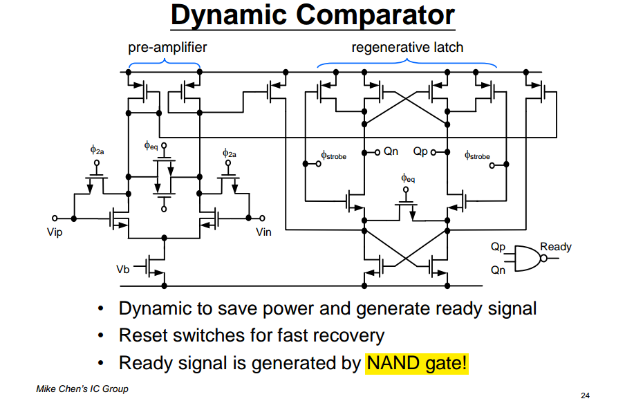
Comparator
Comparator input cap effect
\[
-V_{in}\cdot 2^N C = V_c (2^N C + C_p)
\] Then \(V_c = -\frac{2^N C}{2^N C +
C_p}V_{in}\), i.e. this capacitance reduce the voltage amplitude
by the factor
During conversion \[\begin{align}
V_c &= -\frac{2^N C}{2^N C + C_p}V_{in} +V_{ref}\sum_{n=0}^{N-1}
\frac{b_n\cdot2^n C}{2^N C + C_p} \\
&= \frac{2^N C}{2^N C + C_p}\left(-V_{in} +
V_{ref}\sum_{n=0}^{N-1}\frac{b_n }{2^{N-n}} \right)
\end{align}\]
That is, it does not change the sign
Comparator offset effect
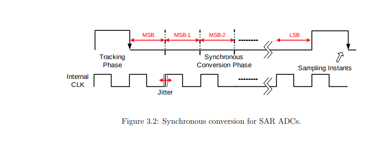
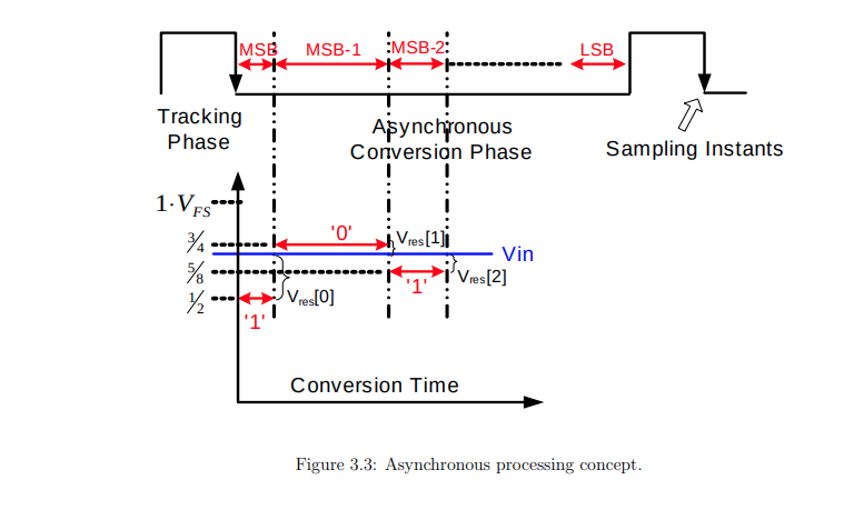
Synchronous SAR ADC
It also divides a full conversion into several comparison stages in a
way similar to the pipeline ADC, except the algorithm is
executed sequentially rather than in parallel
as in the pipeline case.
However, the sequential operation of the SA algorithm has
traditionally been a limitation in achieving high-speed
operation
a clock running at least \((N + 1) \cdot
F_s\) is required for an \(N\)-bit converter with conversion rate of
\(F_s\)
every clock cycle has to tolerate the worst case comparison
time
every clock cycle requires margin for the clock jitter
The power and speed limitations of a synchronous SA design comes
largely from the high-speed internal clock
The comparator itself trigger the next bit-conversion cycle as soon
as the present bit decision has been taken
The maximum resolving time reduction between synchronous and
asynchronous case is two fold
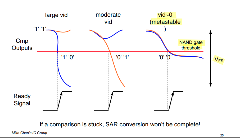
comparator metastable state
when the input is sufficiently small. The time needed for
the comparator outputs to fully resolve may take arbitrarily
long
In this case, the ready signal generator should still set the
flag and the decision result is simply taken from the previous
value stored in the SR latch
both outputs (\(Q_p\) and \(Q_n\)) will drop together, NAND is
inverter actually
The transition point of this NAND gate is skewed to
eliminate metastability issues arising when the input differential
voltage level is small (comparator)
reference
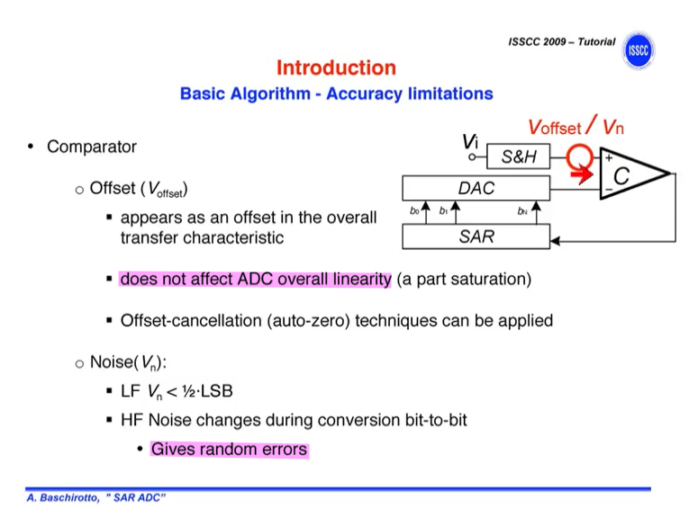
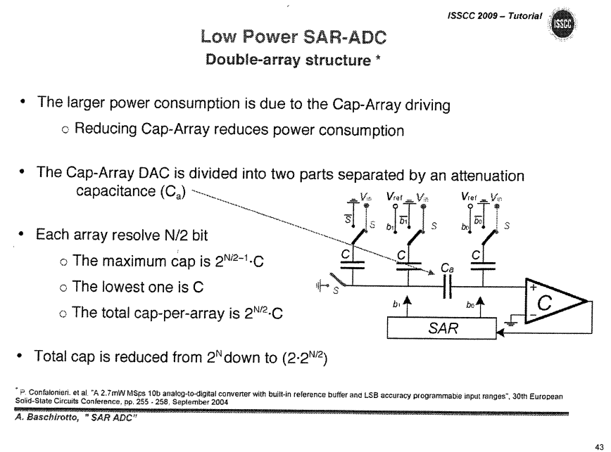
Andrea Baschirotto, "T6: SAR ADCs" ISSCC2009
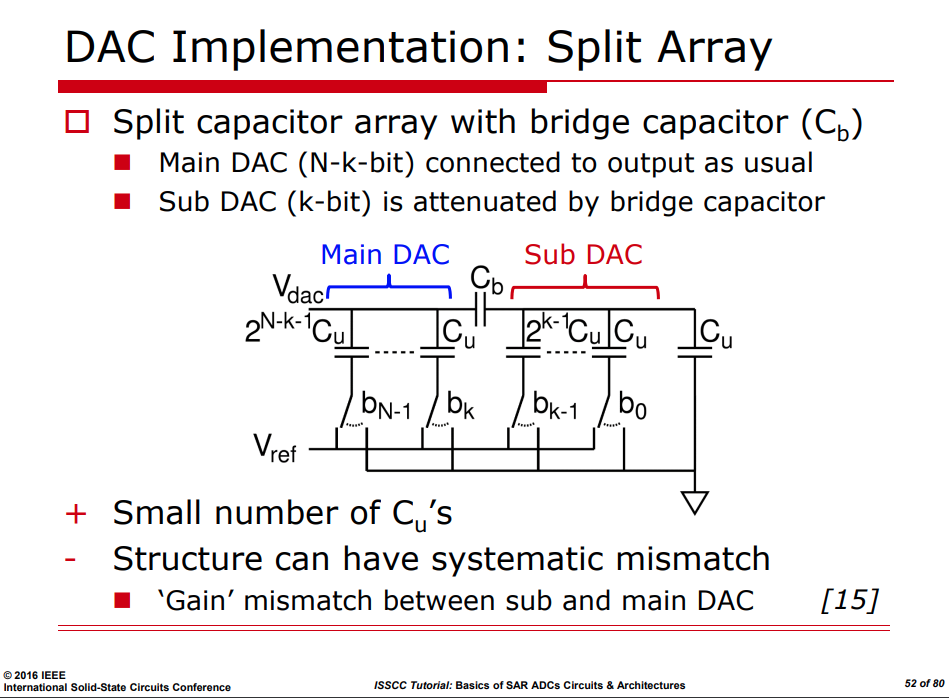
Pieter Harpe, ISSCC 2016 Tutorial: "Basics of SAR ADCs Circuits &
Architectures"
Mike Shuo-Wei Chen and R. W. Brodersen, "A 6-bit 600-MS/s 5.3-mW
Asynchronous ADC in 0.13-μm CMOS," in IEEE Journal of Solid-State
Circuits, vol. 41, no. 12, pp. 2669-2680, Dec. 2006 [pdf,
slides]
C. -C. Liu, S. -J. Chang, G. -Y. Huang and Y. -Z. Lin, "A 10-bit
50-MS/s SAR ADC With a Monotonic Capacitor Switching Procedure," in
IEEE Journal of Solid-State Circuits, vol. 45, no. 4, pp.
731-740, April 2010 [https://sci-hub.se/10.1109/JSSC.2010.2042254]
L. Jie et al., "An Overview of Noise-Shaping SAR ADC: From
Fundamentals to the Frontier," in IEEE Open Journal of the Solid-State
Circuits Society, vol. 1, pp. 149-161, 2021 [pdf]
W. Liu, P. Huang and Y. Chiu, "A 12-bit, 45-MS/s, 3-mW Redundant
Successive-Approximation-Register Analog-to-Digital Converter With
Digital Calibration," in IEEE Journal of Solid-State Circuits, vol. 46,
no. 11, pp. 2661-2672, Nov. 2011 [https://sci-hub.st/10.1109/JSSC.2011.2163556]
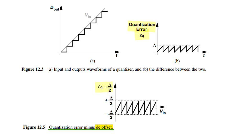
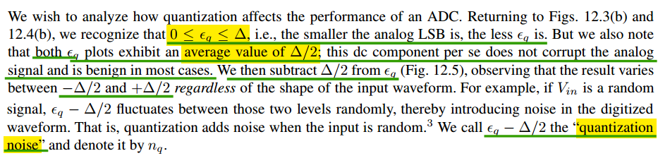
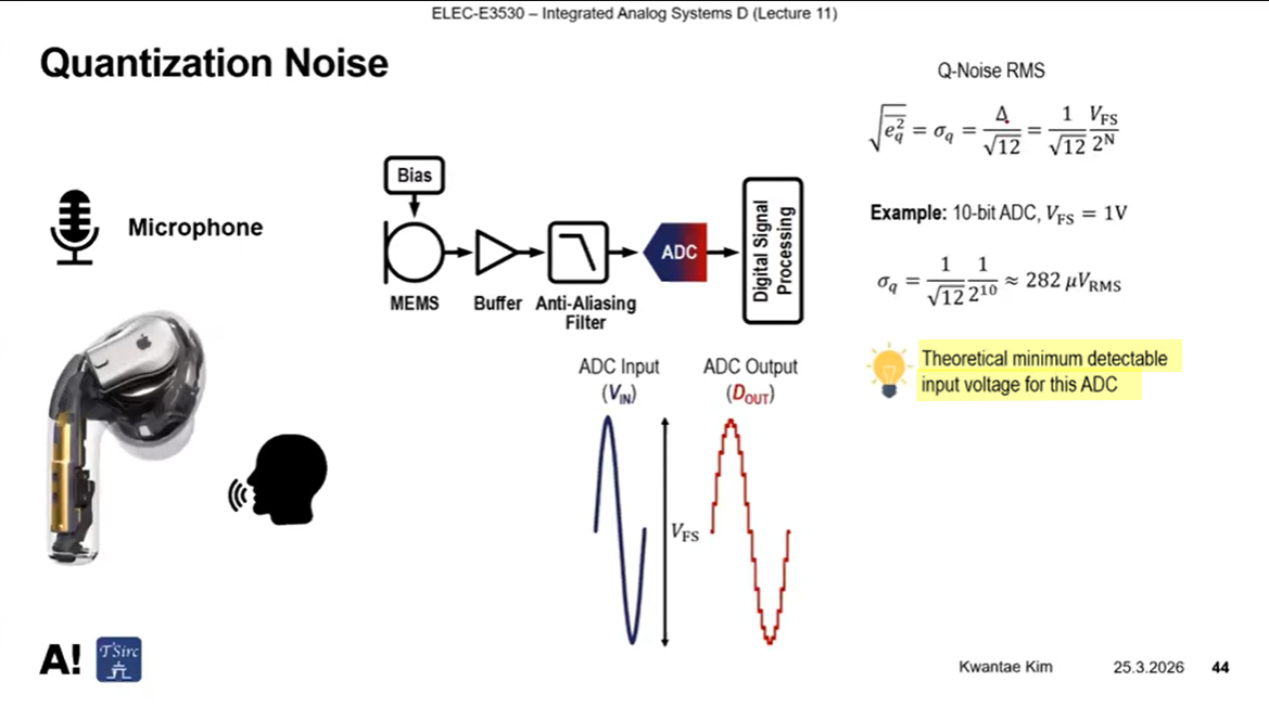
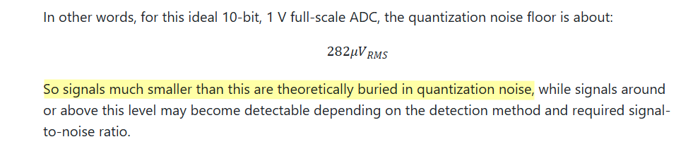
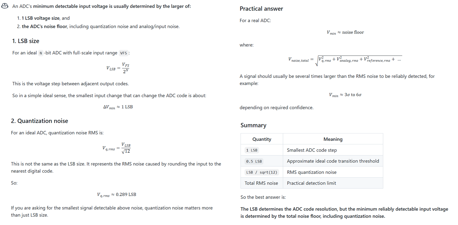
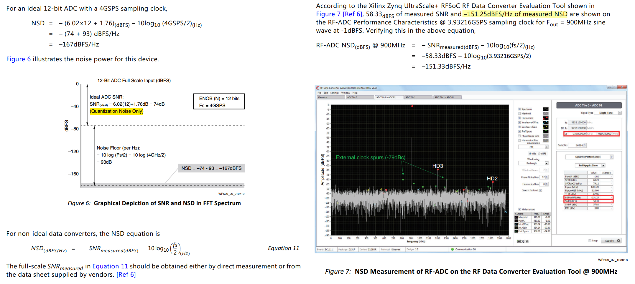
The LSB determines the ADC code resolution, but the minimum reliably
detectable input voltage is determined by the total noise floor,
including quantization noise
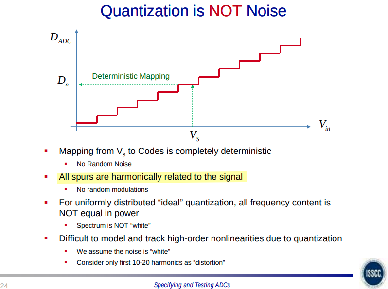
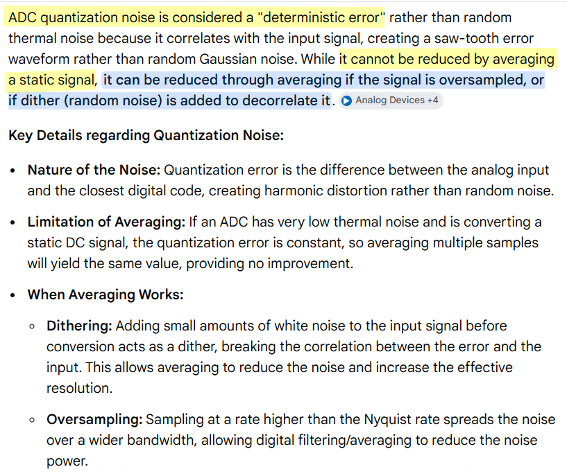
ADC quantization noise is considered a "deterministic error" rather
than random thermal noise because it correlates with the input signal,
creating a saw-tooth error waveform rather than random Gaussian noise.
While it cannot be reduced by averaging a static signal, it
can be reduced through averaging if the signal is
oversampled, or if dither (random noise) is added to decorrelate it.
Quantization is NOT Noise
N. Blachman, "The intermodulation and distortion due to quantization
of sinusoids," in IEEE Transactions on Acoustics, Speech, and Signal
Processing, vol. 33, no. 6, pp. 1417-1426, December 1985 [https://sci-hub.st/10.1109/TASSP.1985.1164729]
N. Blachman, "The intermodulation and distortion due to quantization
of sinusoids," in IEEE Transactions on Acoustics, Speech, and Signal
Processing, vol. 33, no. 6, pp. 1417-1426, December 1985
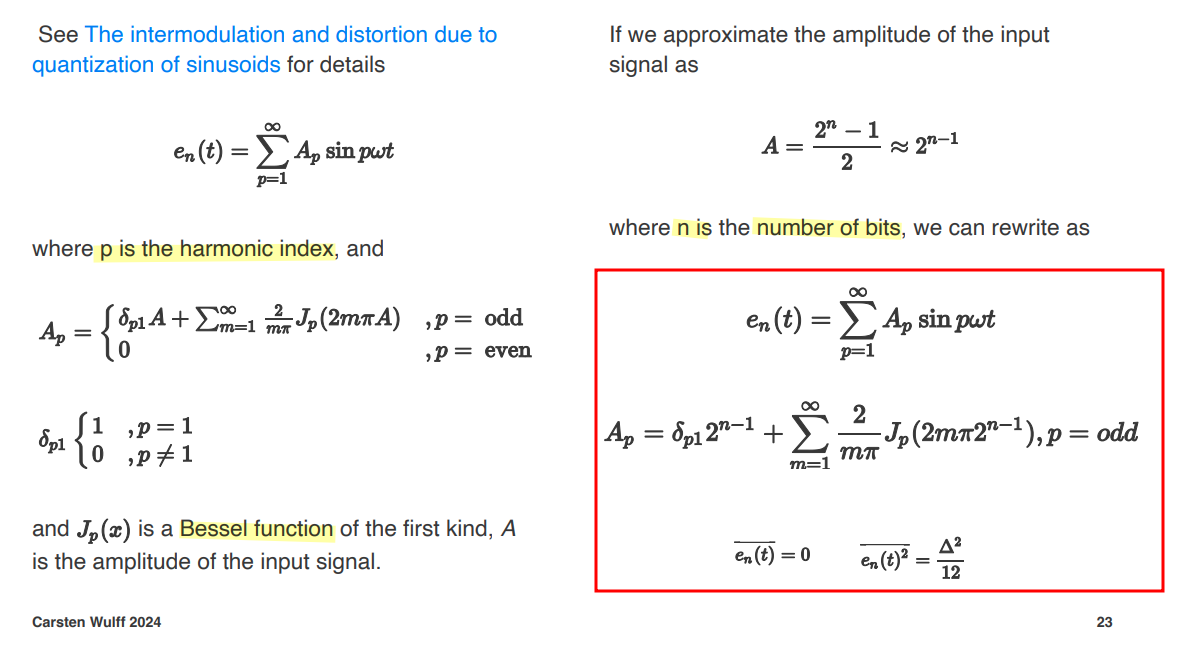
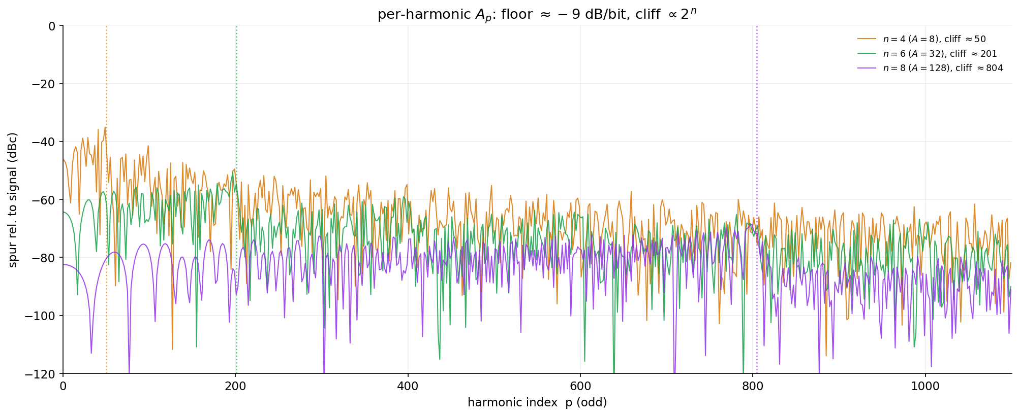
The quantization noise is an infinite sum of input signal
odd harmonics, where the amplitude of the harmonics is
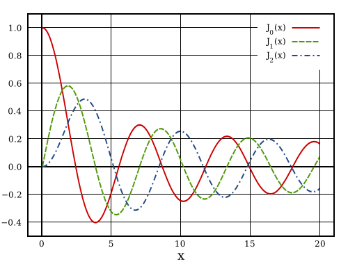
determined by a sum of a Bessel function
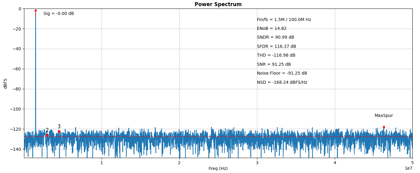
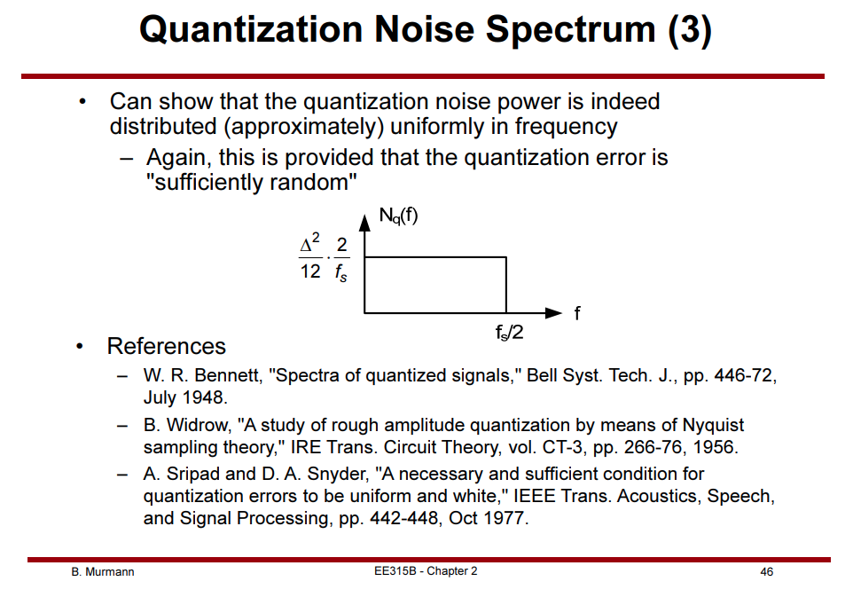
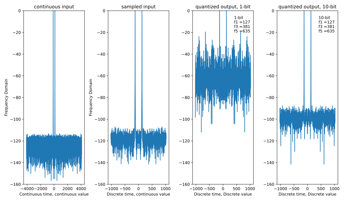
"Quantization noise is white", because for a high
number of bits, it looks white in the FFT
The quantization noise is odd harmonics of the input
signal [Gist
link]
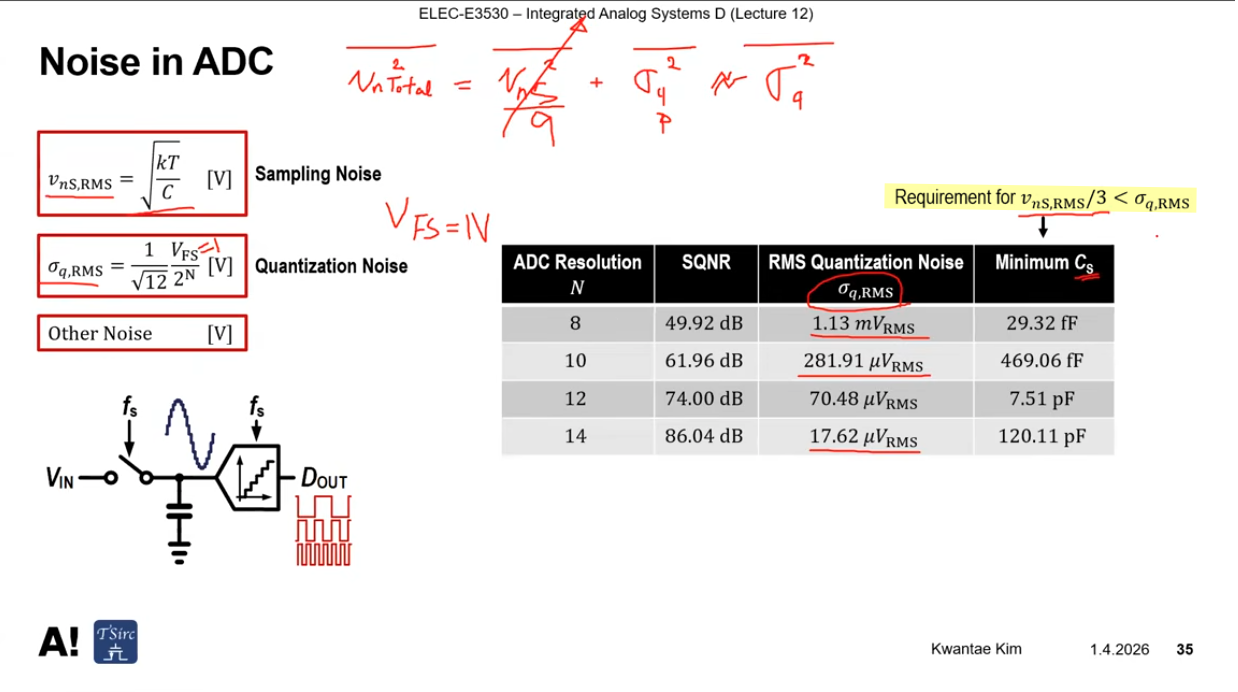
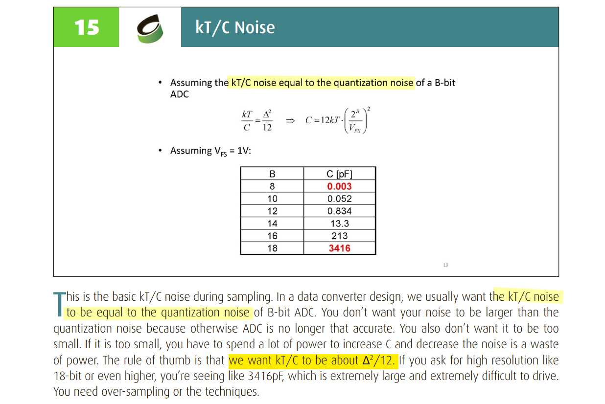
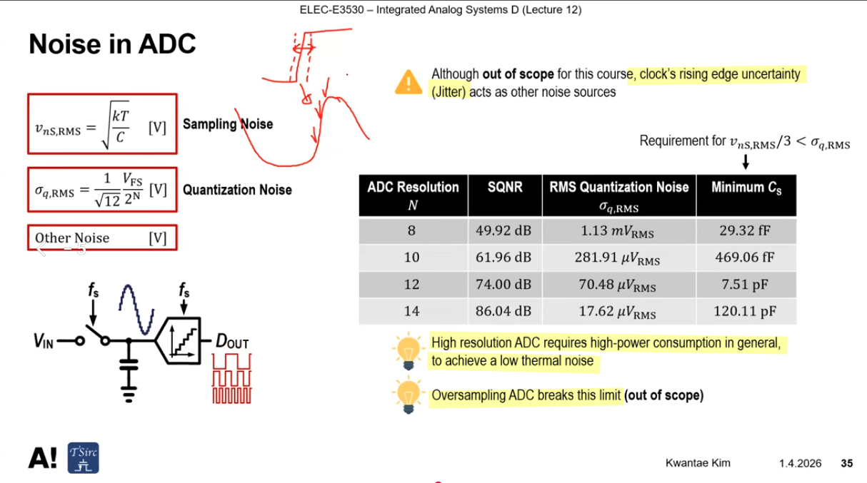
In the power domain, \(\color{red}v_{nS,RMS}/3 \lt
\sigma_{q,RMS}\) ensures that sampling noise power is nearly
an order of magnitude smaller than the quantization noise
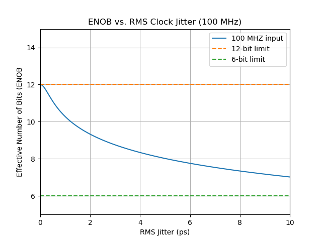
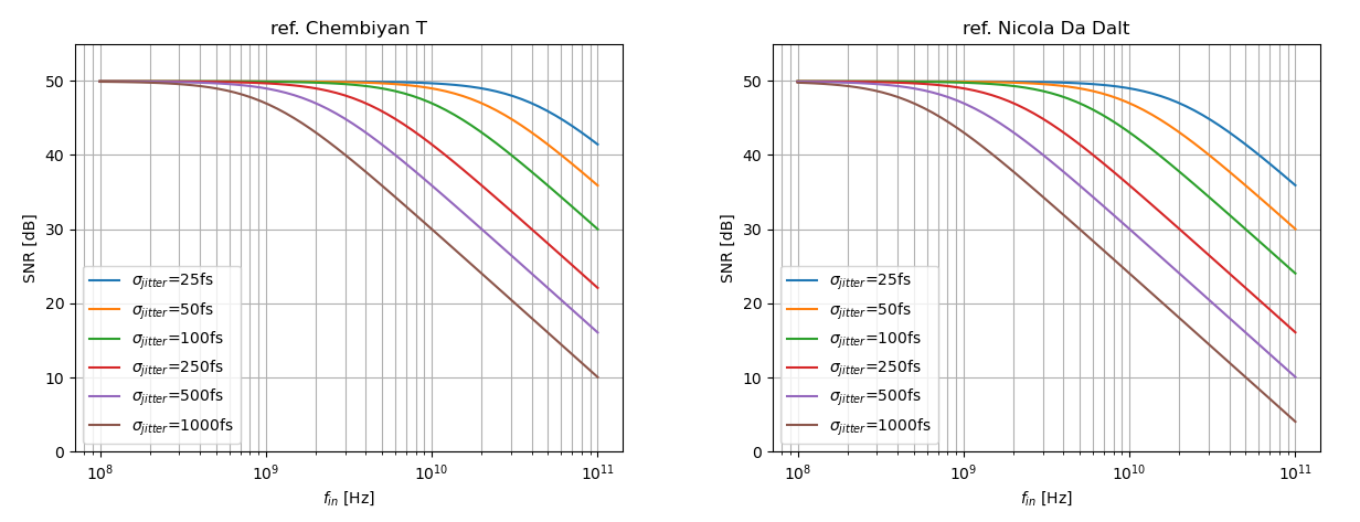
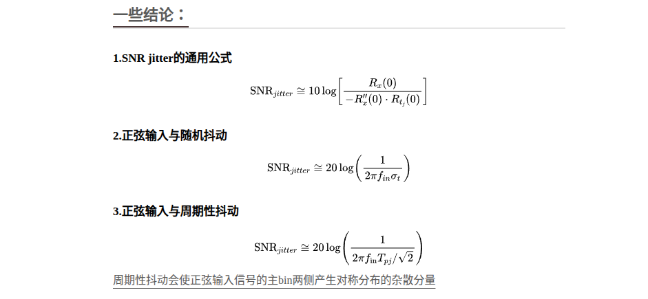
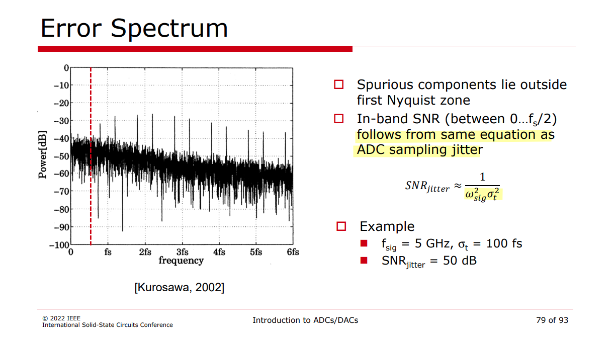
ADC SNR & clock jitter
Akkaya, A. (2021). High-Speed ADC Design and Optimization for
Wireline Links (Publication No. 8453) [PhD thesis, EPFL; Supervised by
Y. Leblebici]. [https://doi.org/10.5075/epfl-thesis-8453]
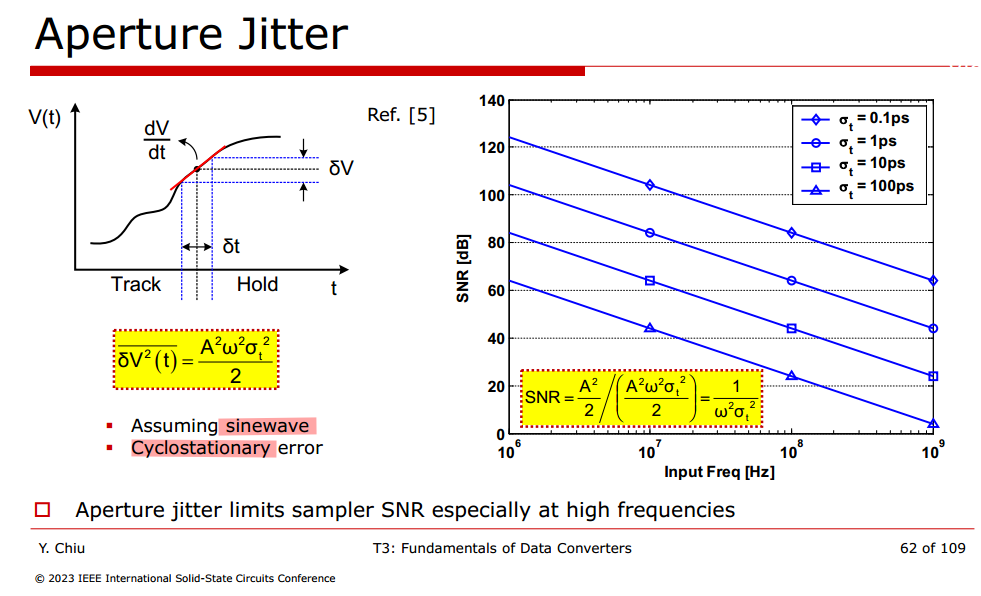
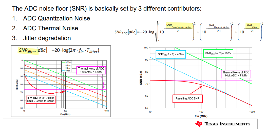
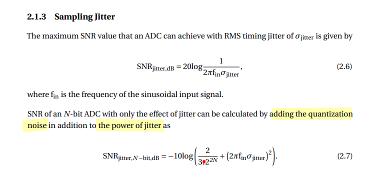
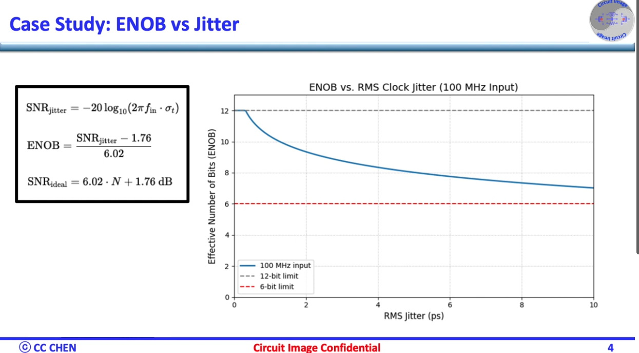
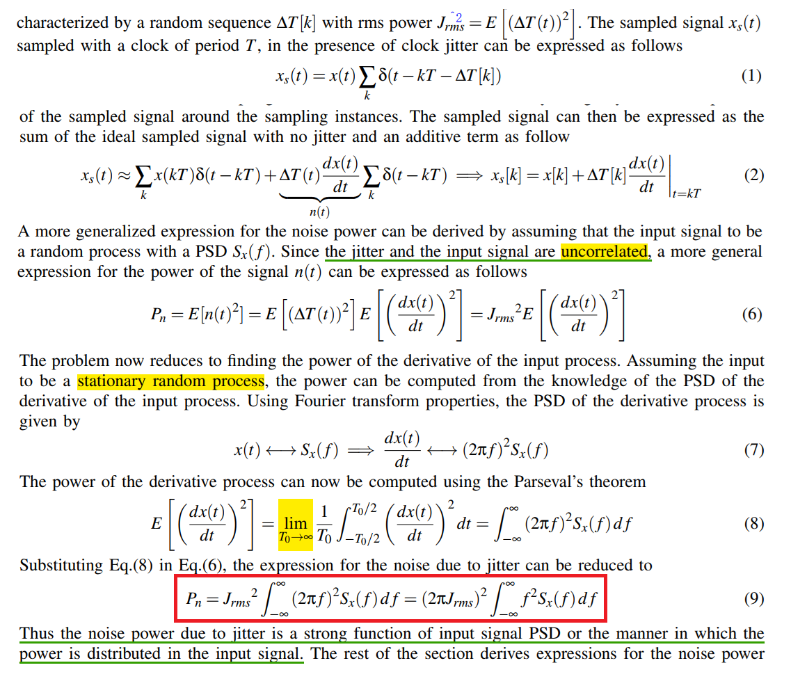
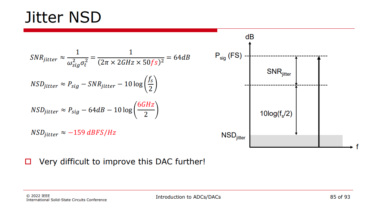
Unlike the quantization noise and the thermal noise, the impact of
the clock jitter on the ADC performance depends on the input signal
properties like its PSD
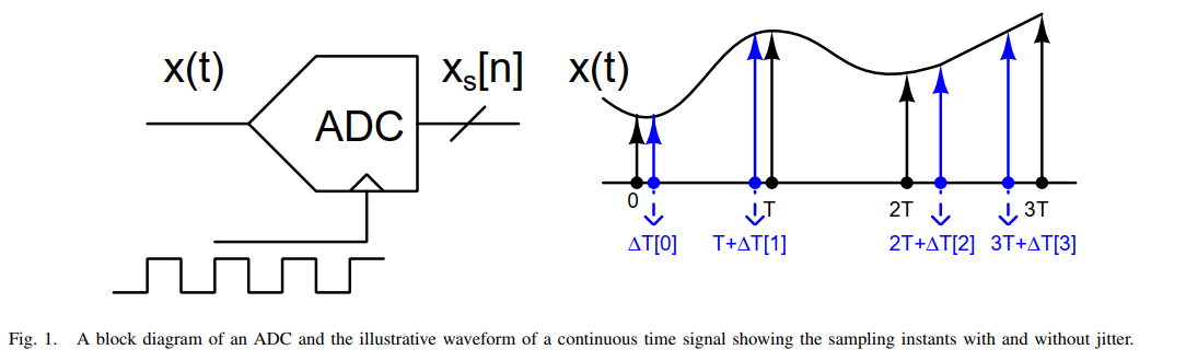
The error between the ideal sampled signal and the
sampling with clock jitter can be treated as noise and it results
in the degradation of the SNR of the ADC
K. Tyagi and B. Razavi, "Performance Bounds of ADC-Based Receivers
Due to Clock Jitter," in IEEE Transactions on Circuits and Systems
II: Express Briefs, vol. 70, no. 5, pp. 1749-1753, May 2023 [https://www.seas.ucla.edu/brweb/papers/Journals/KT_TCAS_2023.pdf]
N. Da Dalt, M. Harteneck, C. Sandner and A. Wiesbauer, "On the jitter
requirements of the sampling clock for analog-to-digital converters," in
IEEE Transactions on Circuits and Systems I: Fundamental Theory and
Applications, vol. 49, no. 9, pp. 1354-1360, Sept. 2002 [https://sci-hub.se/10.1109/TCSI.2002.802353]
M. Shinagawa, Y. Akazawa and T. Wakimoto, "Jitter analysis of
high-speed sampling systems," in IEEE Journal of Solid-State Circuits,
vol. 25, no. 1, pp. 220-224, Feb. 1990 [https://sci-hub.se/10.1109/4.50307]
Akkaya, A. (2021). High-Speed ADC Design and Optimization for
Wireline Links (Publication No. 8453) [PhD thesis, EPFL; Supervised by
Y. Leblebici]. [https://doi.org/10.5075/epfl-thesis-8453]
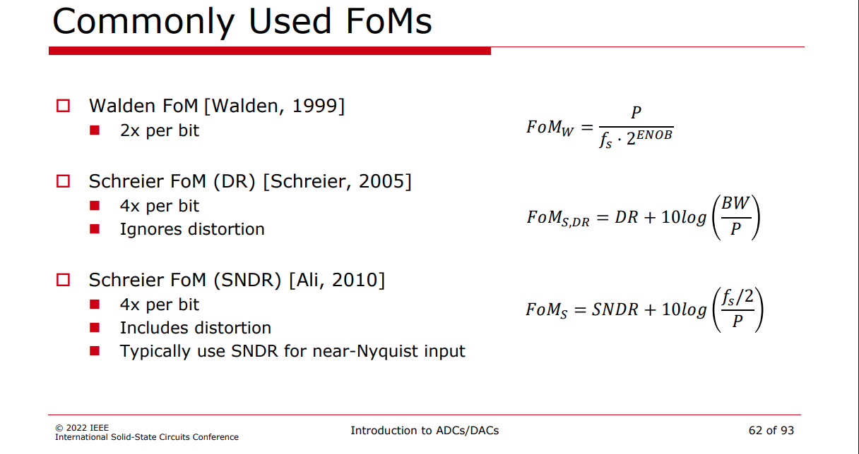
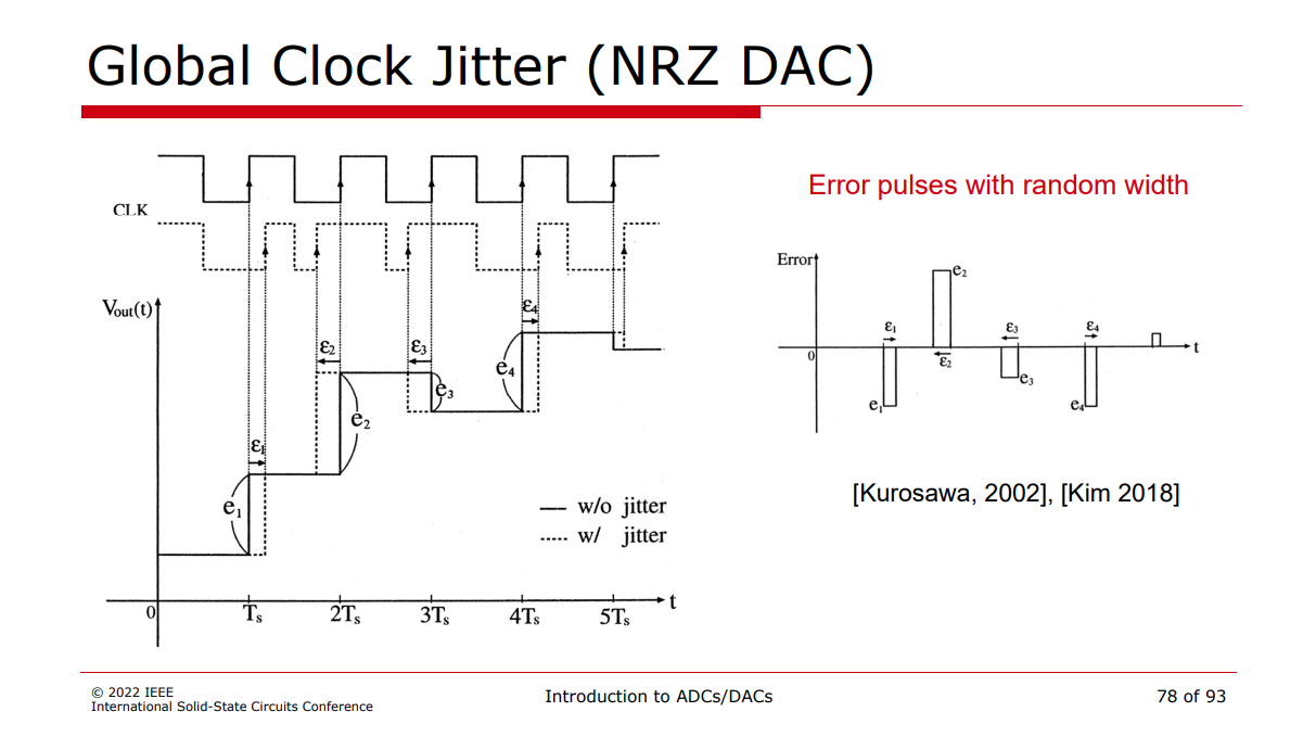
Boris Murmann ISSCC 2022 SC1: Introduction to ADCs/DACs: Metrics,
Topologies, Trade Space, and Applications [pdf]
S. Kim, K. -Y. Lee and M. Lee, "Modeling Random Clock Jitter Effect
of High-Speed Current-Steering NRZ and RZ DAC," in IEEE Transactions
on Circuits and Systems I: Regular Papers, vol. 65, no. 9, pp.
2832-2841, Sept. 2018 [https://sci-hub.se/10.1109/TCSI.2018.2821198]
Martin Clara. High-Performance D/A-Converters - Application to
Digital Transceivers, 2013 [pdf]
Chun-Hsien Su (蘇純賢). Design of Oversampled Sigma-Delta Data
Converters. July, 2006 [pdf]
ampling Jitter Effects for ADC/DAC
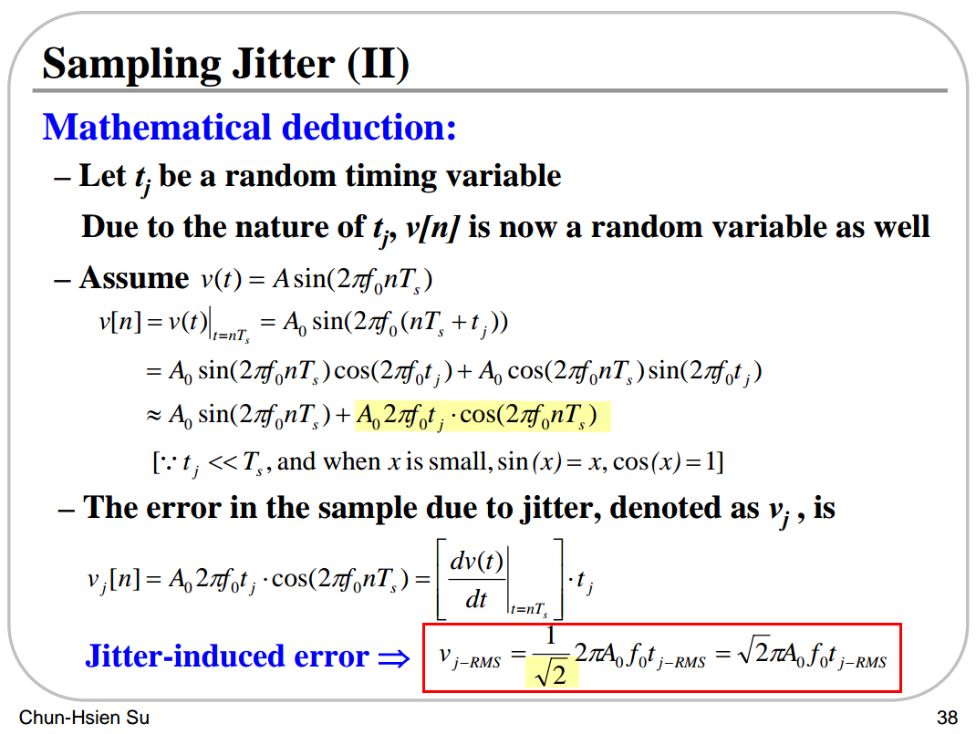
In both DAC or ADC cases, doubling the timing jitter doubles the
noise level
Also, doubling the frequency or amplitude doubles the jitter induced
noise - SNR is not improved
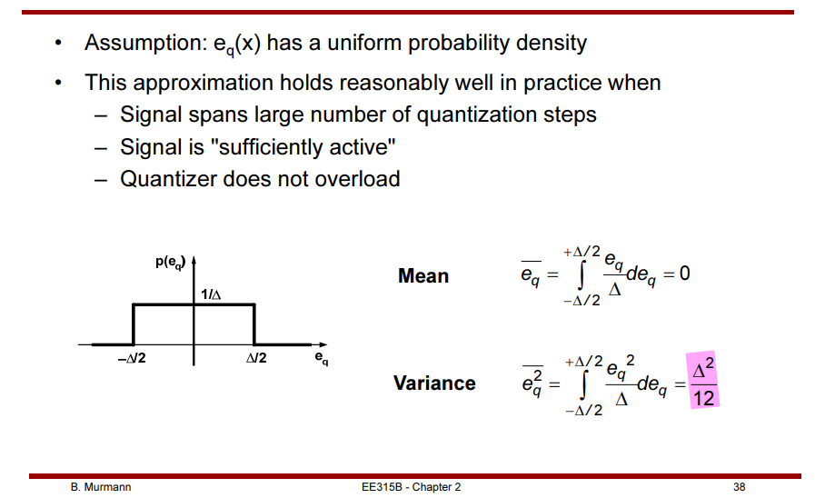
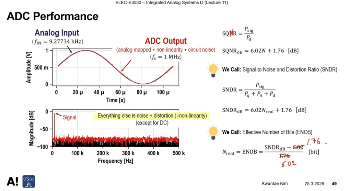
The quantization noise power \(P_Q\)
for a uniform quantizer with step size \(\Delta\) is given by \[
P_Q = \frac{\Delta ^2}{12}
\] For a full-scale sinusoidal input signal with an amplitude
equal to \(V_{FS}/2\), the input signal
is given by \(x(t) =
\frac{V_{FS}}{2}\sin(\omega t)\)
Then input signal power \(P_s\) is
\[
P_s = \frac{V_{FS}^2}{8}
\] Therefore, the signal-to-quantization noise ratio
(SQNR) is given by \[
\text{SQNR} = \frac{P_s}{P_Q} =
\frac{V_{FS}^2/8}{\Delta^2/12}=\frac{V_{FS}^2/8}{V_{FS}^2/(12\times
2^{2N})} = \frac{3\times 2^{2N}}{2}
\] where \(N\) is the number of
quantization bits
When represented in dBs \[
\text{SQNR(dB)} = 10\log(\frac{P_s}{P_Q}) = 10\log(\frac{3\times
2^{2N}}{2})= 20N\log(2) + 10\log(\frac{3}{2})= 6.02N + 1.76
\]
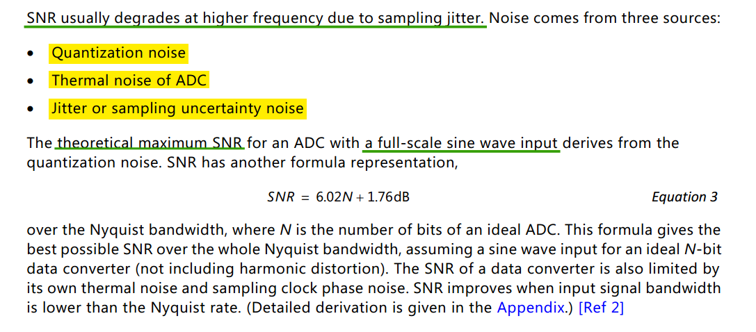
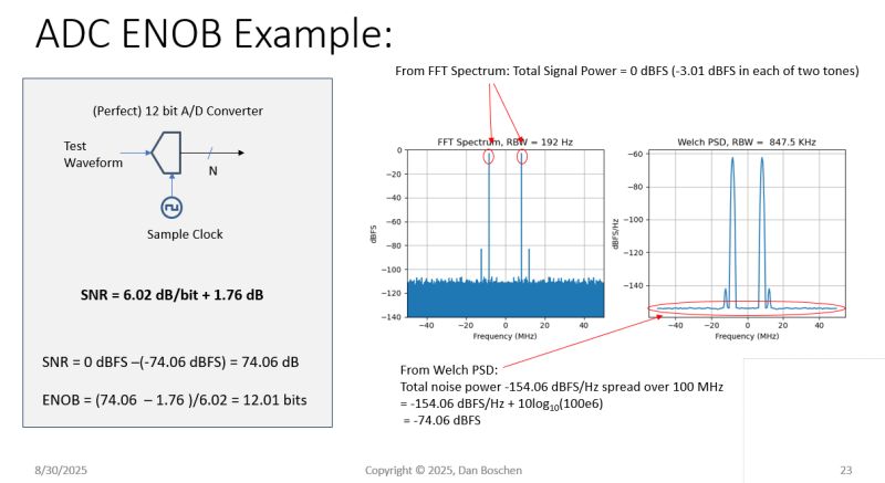
the maximum achievable SNR of N-bit ADC — theoretical SNR limit
Dan Boschen, GRCon25: Quantifying Signal Quality: Practical Tools for
High-Fidelity Waveform Analysis
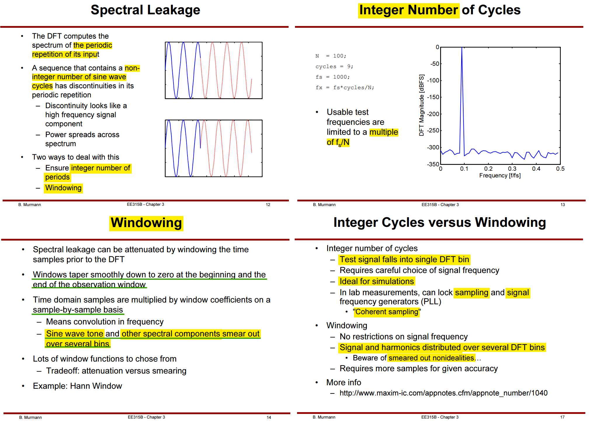
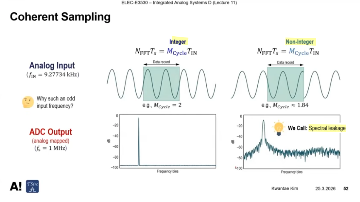
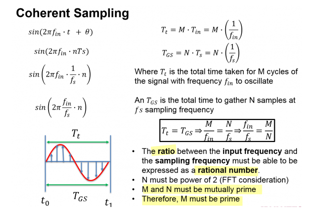
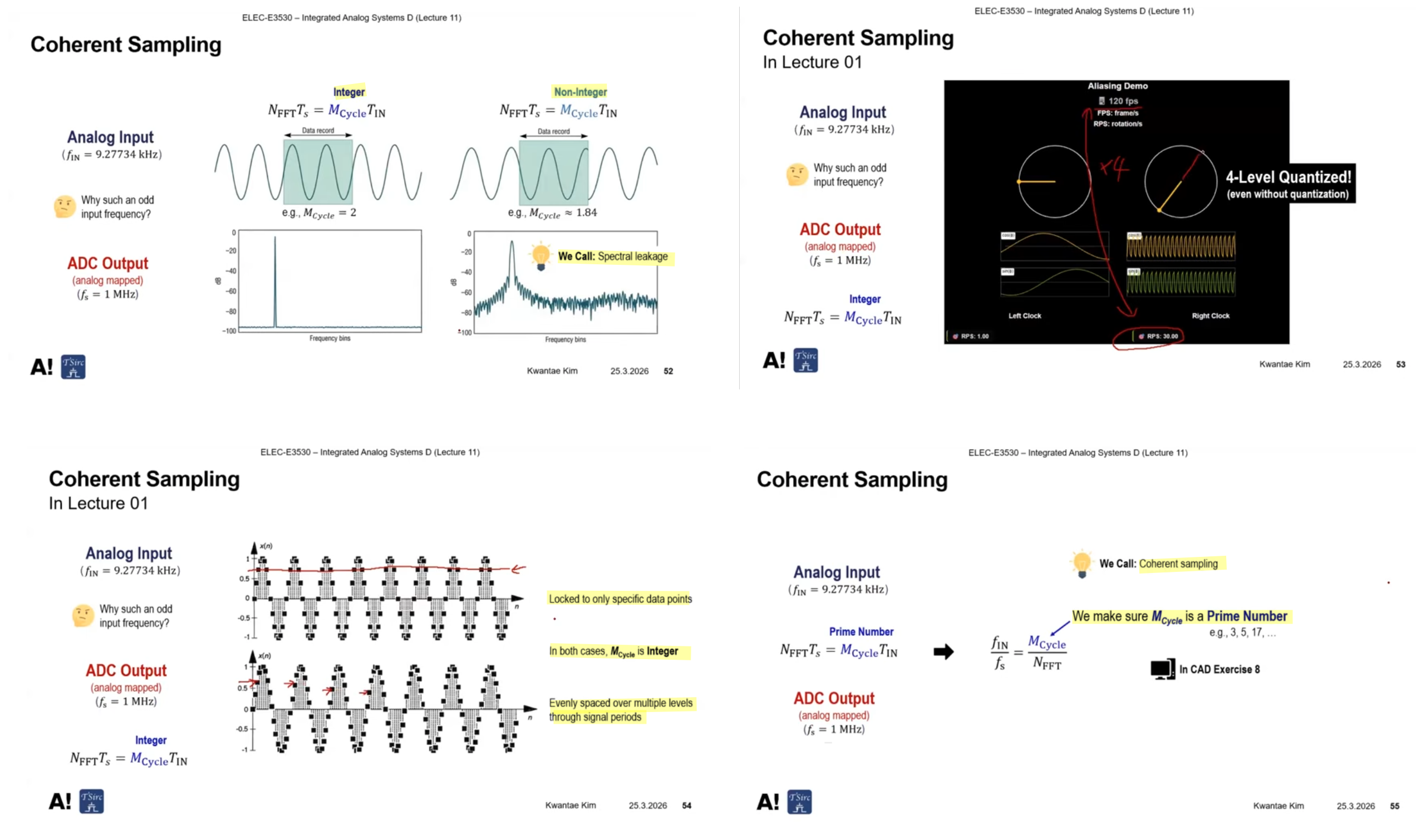
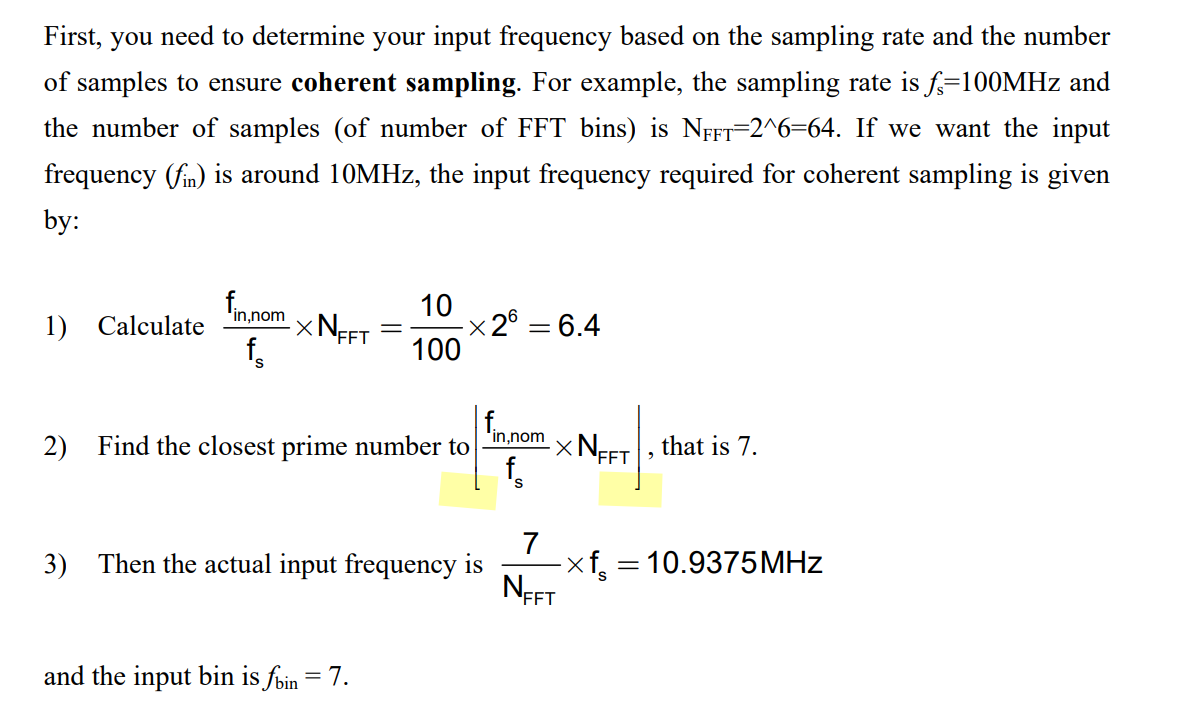
Two ways to deal with spectral leakage: Ensure integer
number of periods or
Windowing
Coherent Sampling
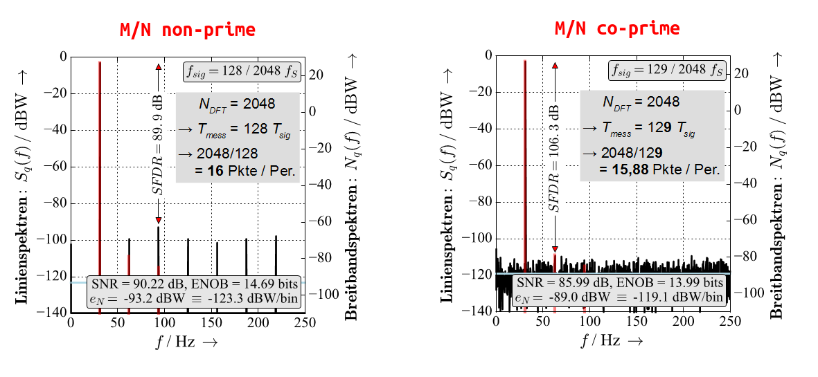
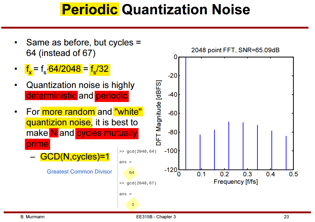
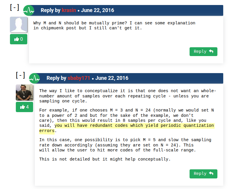
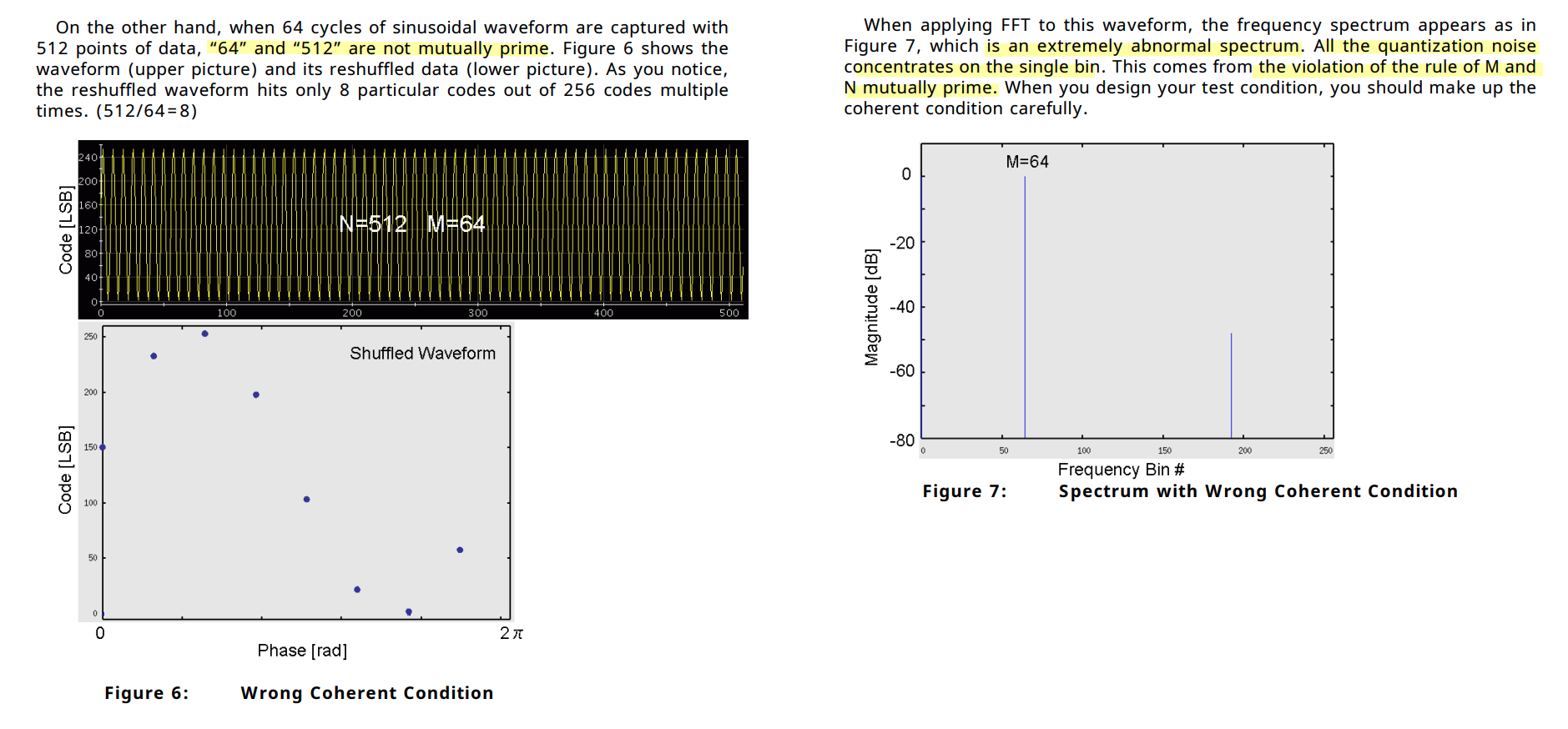
Choosing M/N non-prime repeats the signal quantization periodically
and fewer quantization steps are measured. The quantization repeats
periodically and creates a line spectrum that can obscure real frequency
lines (e.g. the red lines in the images below, created by
non-linearities of the ADC).[https://www.dsprelated.com/thread/469/coherent-sampling-very-brief-and-simple]
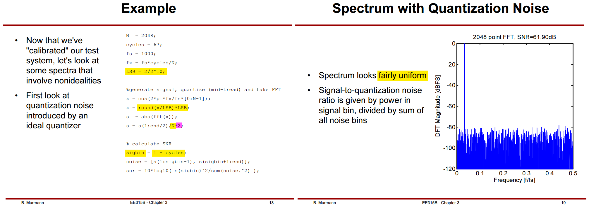
N = 2048;
cycles = 67;
fs = 1000;
fx = fs*cycles/N;
LSB = 2/2^10;
%generate signal, quantize (mid-tread) and take FFT
xc = cos(2*pi*fx/fs*[0:N-1]);
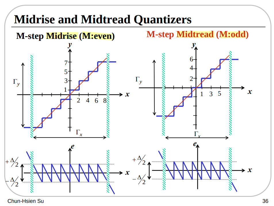
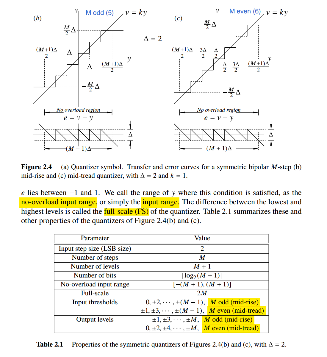
x = round(xc/LSB)*LSB;
s = abs(fft(x));
s = s(1:end/2)/N*2;
% calculate SNR
sigbin = 1 + cycles;
noise = [s(1:sigbin-1), s(sigbin+1:end)];
snr = 10*log10( s(sigbin)^2/sum(noise.^2) );

% frequency vector
f = [0:N/2-1]/N;
subplot(1,3,1)
stem(f, s);

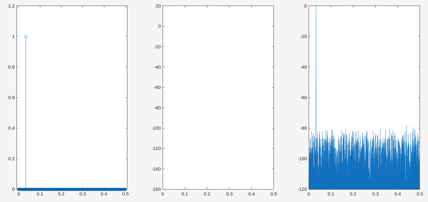
% some FFT bins for "noise" to be exactly zero, empty plot
subplot(1,3,2)
plot(f, 20*log10(s))

% Use a small offset to avoid -Inf
subplot(1,3,3)
plot(f, 20*log10(s + 1e-6))
ylim([-120, 0])
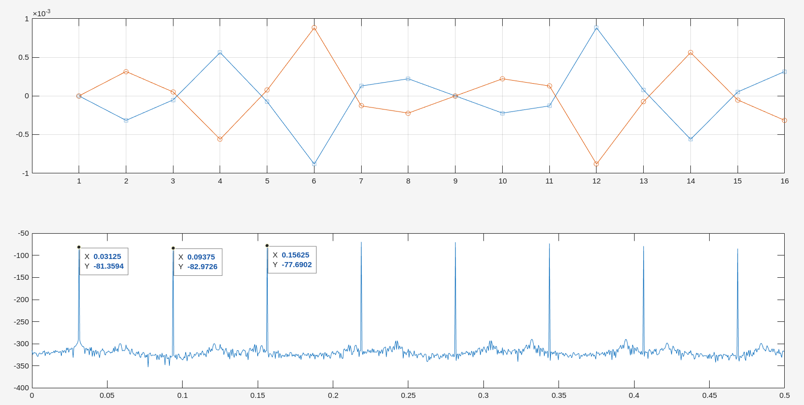
Periodic Quantization Noise if N and cycles
are not mutually prime, i.e.
cycles=64 then GCD(2048, 64)=64, then \(N_R' = 2048/64=32\), so quantization
noise manifests as odd harmonics\(n/32\mid n = 2k + 1, k \in \mathbb{Z}\)
because of Half Wave Symmetry
import numpy as np from matplotlib.ticker import EngFormatter
defcoherent_sampling(fin, Fs, N): """ Returns the adjusted input frequency for coherent sampling. Parameters: fin : input frequency (Hz) Fs : sample rate (Hz) N : number of samples Returns: Adjusted fin (Hz) such that M/N = fin/Fs, where M is the nearest prime to N*fin/Fs. """ x = int(np.ceil(N * fin / Fs)) primes = [n for n inrange(2, x*2) ifall(n % i for i inrange(2, n))] M = primes[np.argmin(np.abs(np.array(primes) - x))] return Fs * M / N
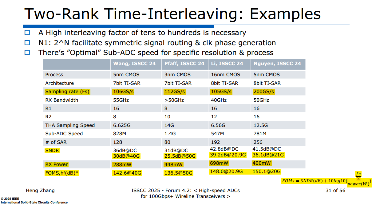
D. Pfaff et al., "7.3 A 224Gb/s 3pJ/b 40dB Insertion Loss
Transceiver in 3nm FinFET CMOS," 2024 IEEE International Solid-State
Circuits Conference (ISSCC), San Francisco, CA, USA, 2024 [https://iccircle.com/static/upload/img20240529101747.pdf]
—, "A 224Gb/s 3pJ/bit 42dB Insertion Loss Post-FEC Error Free
Transceiver in 3-nm FinFET CMOS (Invited)," 2025 IEEE Custom
Integrated Circuits Conference (CICC), Boston, MA, USA, 2025, pp.
1-8, doi: 10.1109/CICC63670.2025.10983461.
E. Swindlehurst et al., "An 8-bit 10-GHz 21-mW Time-Interleaved SAR
ADC With Grouped DAC Capacitors and Dual-Path Bootstrapped Switch," IEEE
Journal of Solid-State Circuits, vol. 56, no. 8, pp. 2347-2359, 2021,
[https://sci-hub.se/10.1109/JSSC.2021.3057372]
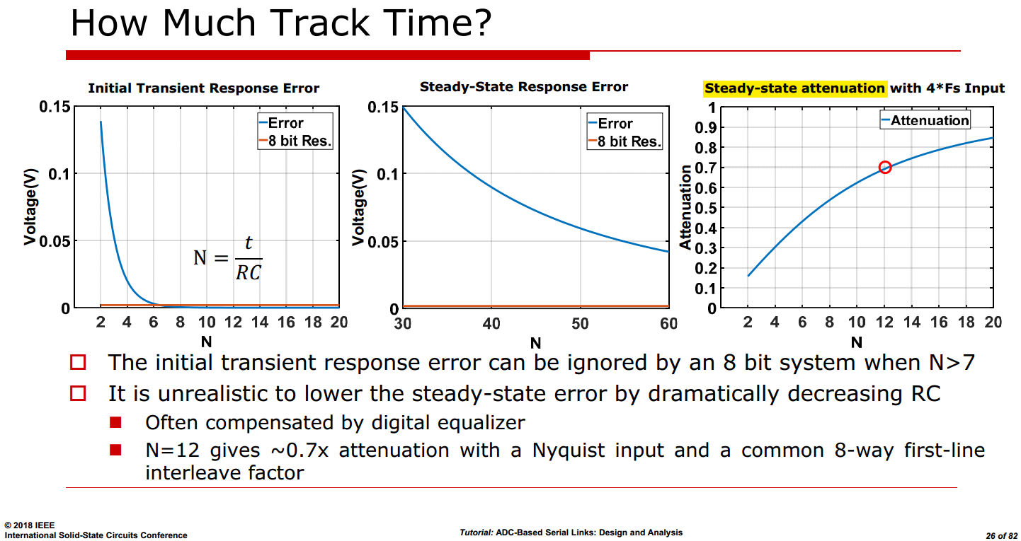
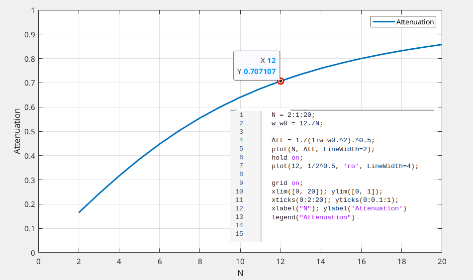
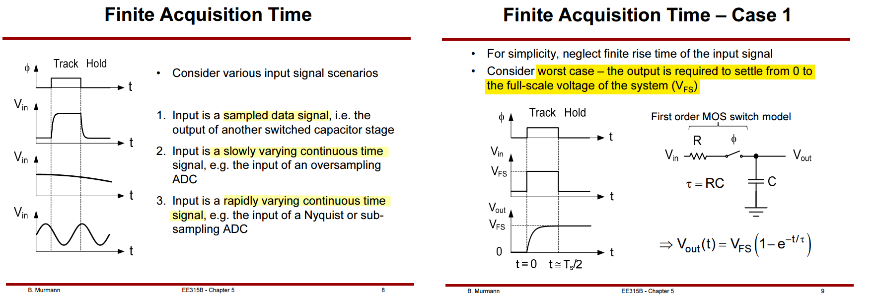
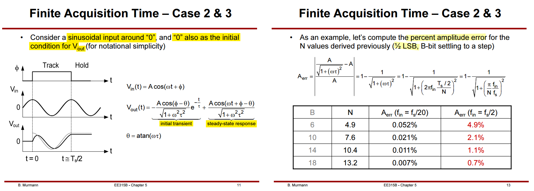
Tracking Settling Accuracy
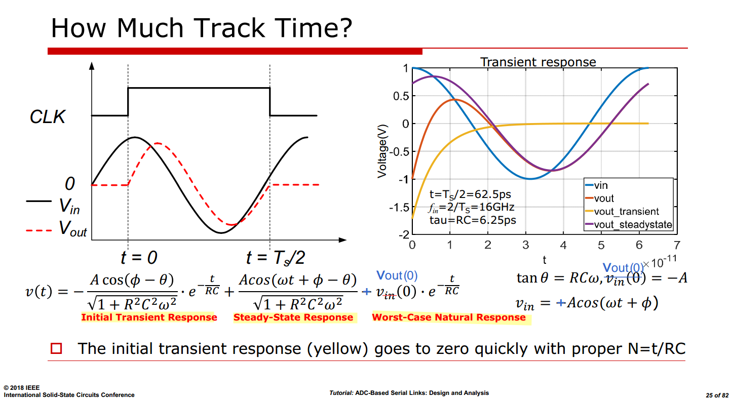
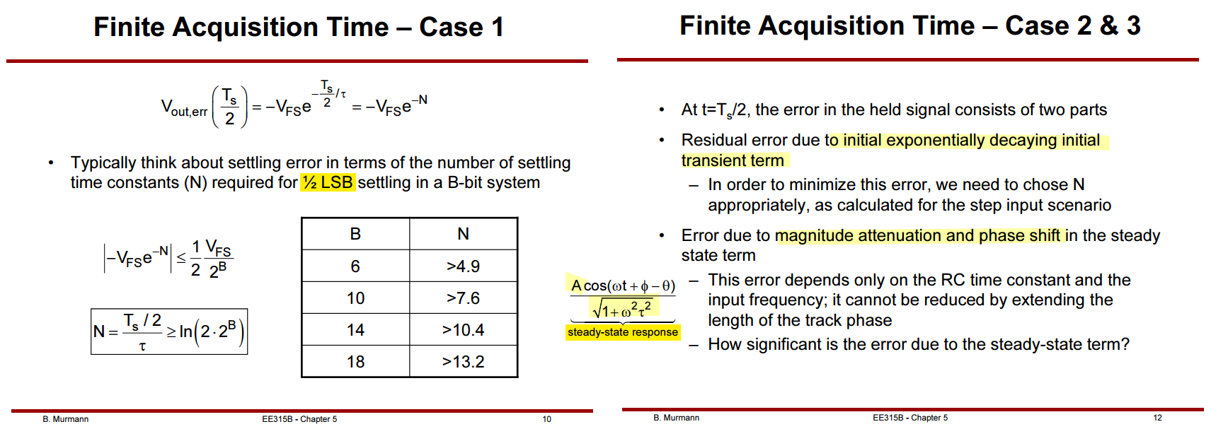
Finite Acquisition Time - Consider a sinusoidal
input
The relation \(V_\text{out}(s) =
H(s)\,V_\text{in}(s)\) is the zero-state
response only. The transfer function is defined under the
assumption \(V_\text{out}(0^-) = 0\),
so you can't recover the natural response from it. You
have to go back one step, to the differential
equation.
Transform with the full derivative rule \(\mathcal{L}\{\dot{V}_\text{out}\} = s
V_\text{out}(s) - V_0\), where \(V_0
\equiv V_\text{out}(0^-)\) (the capacitor voltage is continuous,
so \(0^-\) and \(0^+\) agree): \[
\tau\big(s V_\text{out}(s) - V_0\big) + V_\text{out}(s) = V_\text{in}(s)
\]
\[
\boxed{\;V_\text{out}(s)
= \underbrace{\frac{V_\text{in}(s)}{\tau s + 1}}_{\text{zero-state}}
+ \underbrace{\frac{\tau V_0}{\tau s + 1}}_{\text{zero-input}}
= H(s)\,V_\text{in}(s) + \frac{V_0}{s + \frac{1}{\tau}}\;}
\]
Then the Complete Laplace Expression is \[
\boxed{V_\text{out}(s) = -\frac{\cos(\theta - \phi)}{\sqrt{\omega^2\tau
^2 +1}} \frac{1}{s+\frac{1}{\tau}} + \frac{1}{\sqrt{\omega^2\tau ^2
+1}}\frac{s\cos(\theta - \phi) - \omega \sin(\theta -
\phi)}{s^2+\omega^2} + \frac{V_\text{out}(0)}{s + \frac{1}{\tau}} }
\] The Total Time-Domain Solution\[
\boxed{V_{\text{out}}(t) =
\underbrace{V_{\text{out}}(0)e^{-\frac{t}{\tau}}}_{\text{Pure Natural
Response}} + \underbrace{\frac{1}{\sqrt{\omega^2\tau^2 + 1}} \left[
\cos(\omega t + \theta - \phi) - \cos(\theta - \phi) e^{-\frac{t}{\tau}}
\right]}_{\text{Forced Response (Transient + Steady-State)}}
}
\] And grouped by transient vs. steady-state components: \[
\boxed{V_{\text{out}}(t) = \underbrace{\left[ V_{\text{out}}(0) -
\frac{\cos(\theta - \phi)}{\sqrt{\omega^2\tau^2 + 1}} \right]
e^{-\frac{t}{\tau}}}_{\text{Total Transient Response}} +
\underbrace{\frac{\cos(\omega t + \theta - \phi)}{\sqrt{\omega^2\tau^2 +
1}}}_{\text{Steady-State Response}}}
\]
Tracking Nonlinearity
Wei Yu, Subhajit Sen and B. H. Leung, "Distortion analysis of MOS
track-and-hold sampling mixers using time-varying Volterra series," in
IEEE Transactions on Circuits and Systems II: Analog and Digital Signal
Processing, vol. 46, no. 2, pp. 101-113, Feb. 1999 [https://sci-hub.ru/10.1109/82.752910]
\[\begin{align}
HD_2 &\approx \frac{1}{2}\omega C V_m \frac{\mathcal{d}
R_{on}}{\mathcal{d}v_{in}}\bigg\rvert_{v_{in}=0}=\frac{1}{2}\omega C
V_m\frac{R_{ON}}{V_{OV}} =
\frac{1}{2}\frac{\omega}{\omega_c}\frac{V_m}{V_{OV}} \\
HD_3 &\approx \frac{1}{4}\omega C V_m^2 \frac{\mathcal{d}^2
R_{on}}{\mathcal{d}v_{in}^2}\bigg\rvert_{v_{in}=0}=\frac{1}{4}\omega C
V_m^2\frac{R_{ON}}{V_{OV}^2} =
\frac{1}{2}\frac{\omega}{\omega_c}\left(\frac{V_m}{V_{OV}}\right)^2
\end{align}\]
where \(V_{OV}=V_{DD}-V_{IN}-V_t\),
\(R_{ON}=\frac{1}{\mu
C_{ox}W/LV_{OV}}\) and \(\omega_c=1/R_{ON}C\)
Even-order distortion products cancel in perfectly symmectrical
circuits; But phase and amplitude imbalances lead to finite \(HD_2\) in practice
DAC Settling Accuracy
In a SAR conversion the DAC doesn't move by full
scale — the MSB trial is the largest single
step, and it is exactly half of full scale.
Subsequent trials step by \(V_{FS}/4\),
\(V_{FS}/8\), … So the MSB transition
(\(\color{red}0 \to V_{FS}/2\)) is the
worst case, and if it settles in the allotted per-bit time, every later
trial does too.
The accuracy
criterion
The settling error must stay below half an LSB, where \(\text{LSB} = V_{FS}/2^{n}\):
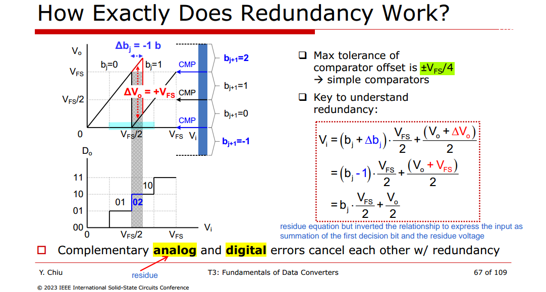
Max tolerance of comparator offset is \(\pm
V_{FS}/4\)
\(b_j\) error is \(\pm 1\)
\(b_{j+1}\) error is \(\pm 2\) , wherein \(b_{j+1}\): \(0\to
2\) or \(1\to -1\)
i.e. complementary analog and digital errors cancel each other, \(V_o +\Delta V_{o}\) should be in
over-/under-range comparators (\(-V_{FS}/2 \sim 3V_{FS}/2\))
Krämer, M. et al. (2015) High-resolution SAR A/D converters with
loop-embedded input buffer. dissertation. Available at: [http://purl.stanford.edu/fc450zc8031].
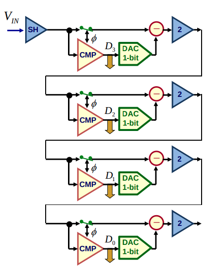
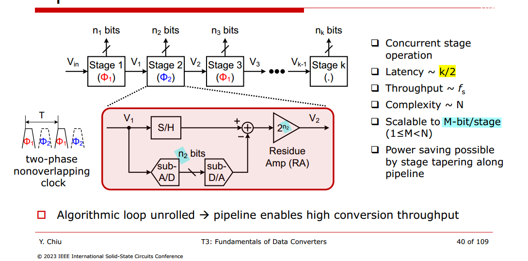
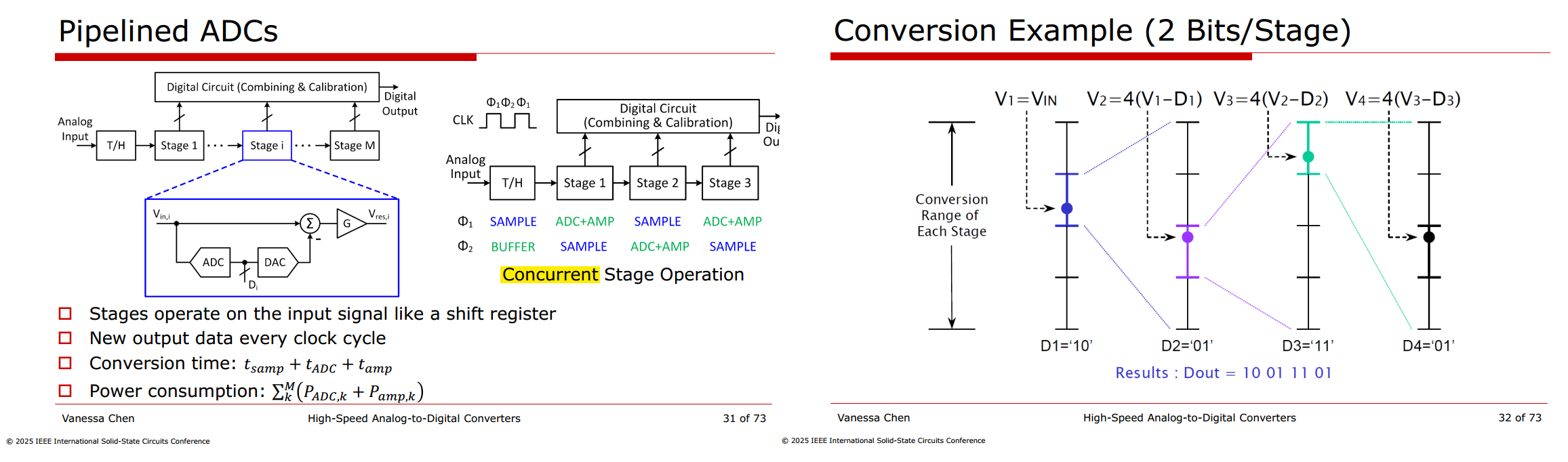
It divides the process into several comparison stages, the number of
which is proportional to the number of bits
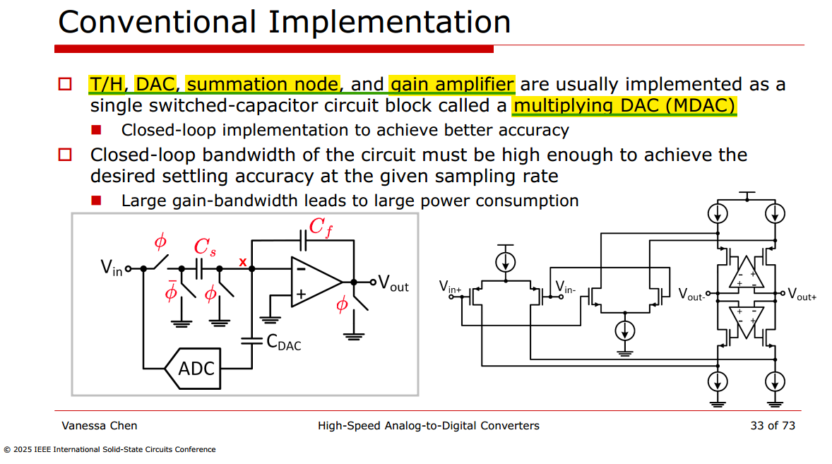
Due to the pipeline structure of both analog and digital signal path,
inter-stage residue amplification is needed which
consumes considerable power and limits high speed operation
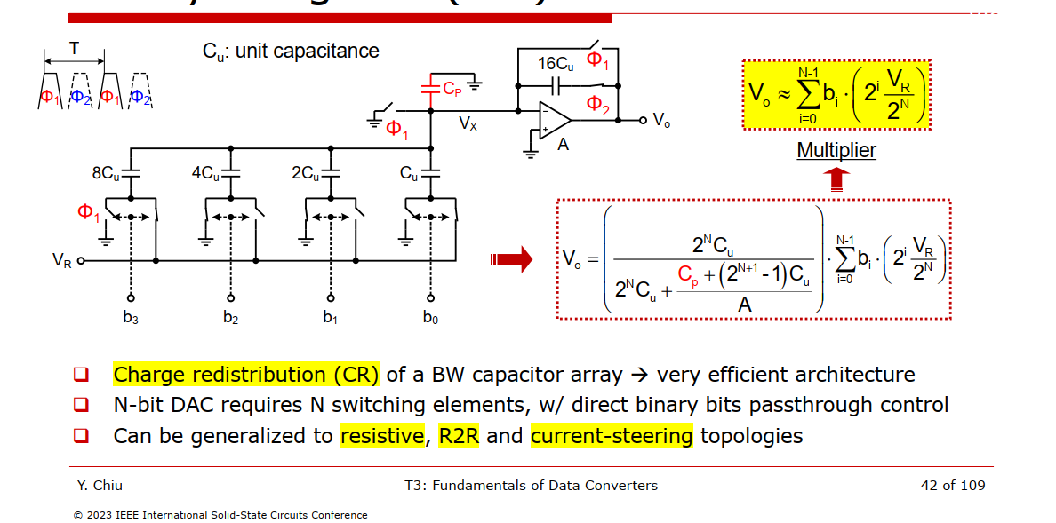
During \(\Phi_1\), all capacitor are
shorted, the net charge at \(V_x\) is
0
During \(\Phi_2\), the charge at
bottom plate of CDAC \[
Q_{DAC,btm} = \sum_{i=0}^{N-1}(b_i\cdot V_R - V_x)\cdot 2^{i}C_u =
C_uV_R\sum_{i=0}^{N-1}b_i2^i - (2^N-1)C_uV_x
\] the charge at the internal plate of integrator \[
Q_{intg} = V_x C_p + (V_x - V_o)2^NC_u
\] and we know \(-V_x A = V_o\)
and \(Q_{DAC,btm} = Q_{intg}\)\[
C_uV_R\sum_{i=0}^{N-1}b_i2^i - (2^N-1)C_uV_x = V_x C_p + (V_x -
V_o)2^NC_u
\] i.e. \[
C_uV_R\sum_{i=0}^{N-1}b_i2^i = (2^N-1)C_uV_x + V_x C_p + (V_x -
V_o)2^NC_u
\] therefore \[
-V_o = \frac{2^N
C_u}{\frac{(2^{N+1}-1)C_u+C_p}{A}+2^NC_u}\sum_{i=0}^{N-1}b_i\left(2^i\frac{V_R}{2^N}\right)\approx
\sum_{i=0}^{N-1}b_i\left(2^i\frac{V_R}{2^N}\right)
\]
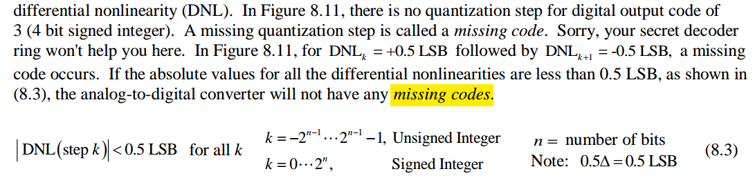
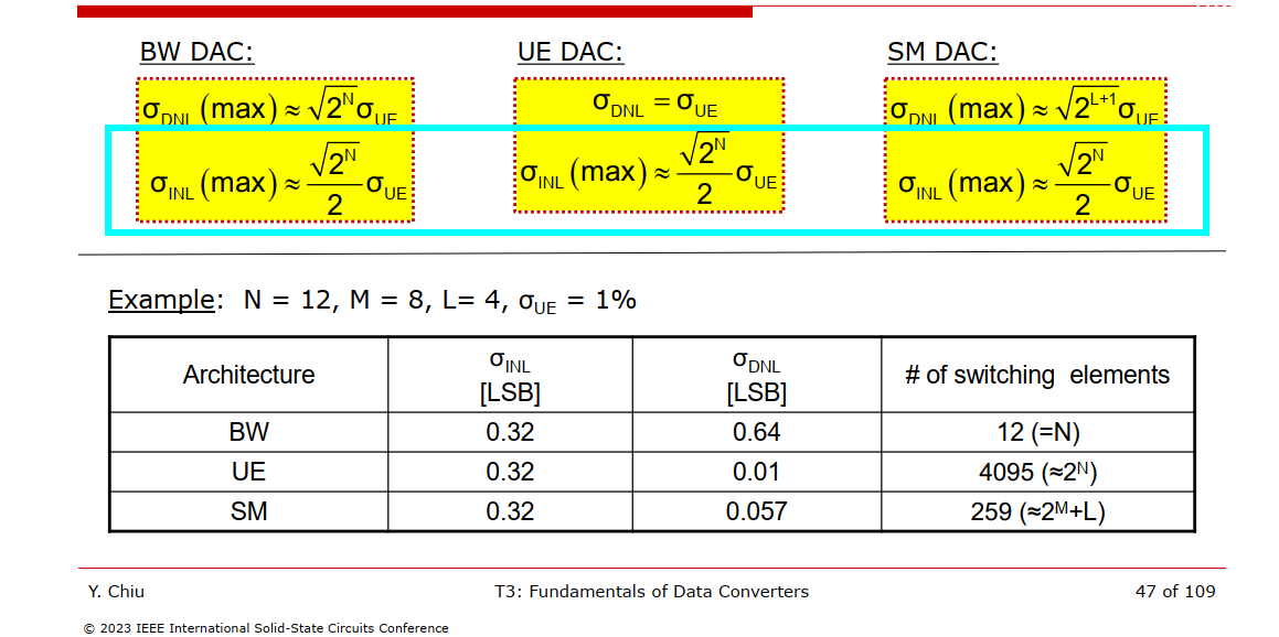
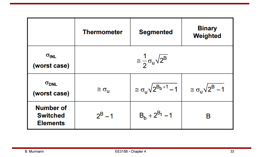
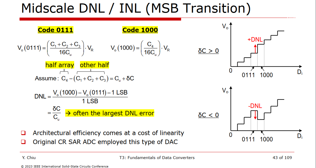
Midscale (MSB Transition) often is the largest DNL
error
\(C_4\) and \(C_1+C_2+C_3\) are independent (can't cancel
out) and their variance is two largest (\(16\sigma_u^2\), \(15\sigma_u^2\), ), the total standard
deviation is \(\sqrt{16\sigma_u^2+15\sigma_u^2}=\sqrt{31}\sigma_u\)
reference
Maloberti, F. Data Converters. Dordrecht, Netherlands:
Springer, 2007.
Ali, Ahmed M. A. High Speed Data Converters. The Institution
of Engineering and Technology, 2016.
Razavi B. Analysis and Design of Data Converters. Cambridge
University Press; 2025.
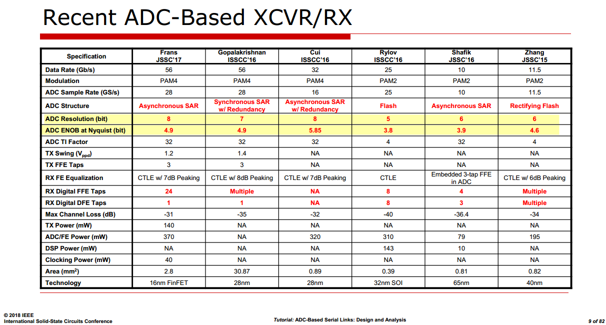
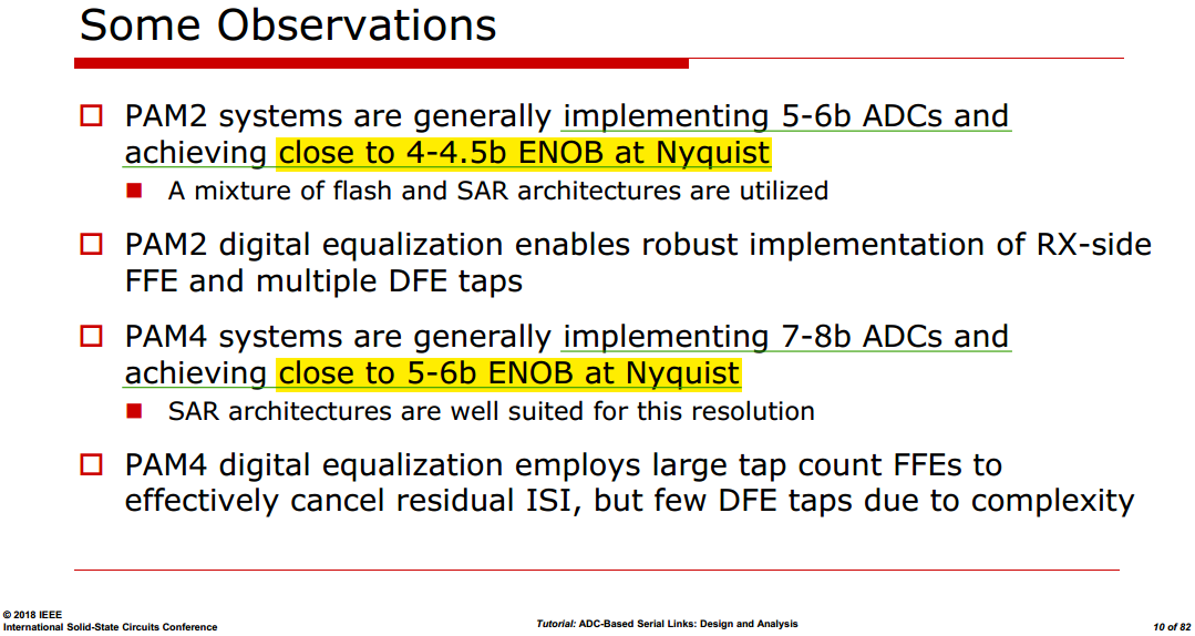
Samuel Palermo, ISSCC 2018 T10: ADC-Based Serial Links: Design and
Analysis
Jan Mulder Broadcom. ISSCC2015 T5: High-Speed Current-Steering
DACs
Zhang, Milin, Zhihua Wang, Jan van der Spiegel and Franco Maloberti.
"Advanced Tutorial on Analog Circuit Design." (2023)
V. Chen, "Tutorial: High-Speed Analog-to-Digital Converters,"
2025 IEEE International Solid-State Circuits Conference
(ISSCC), San Francisco, CA, USA, 2025, pp. 1-1, doi:
10.1109/ISSCC49661.2025.11076112.
S. Su, "Principles and Practices of High-Speed DAC Design: From
Conversion Fundamentals to Layout-Aware Implementation," in IEEE
Solid-State Circuits Magazine, vol. 18, no. 3, pp. 26-43, Summer
2026, doi: 10.1109/MSSC.2026.3704105
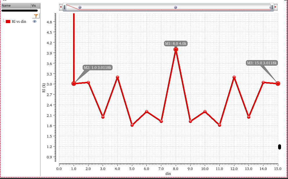
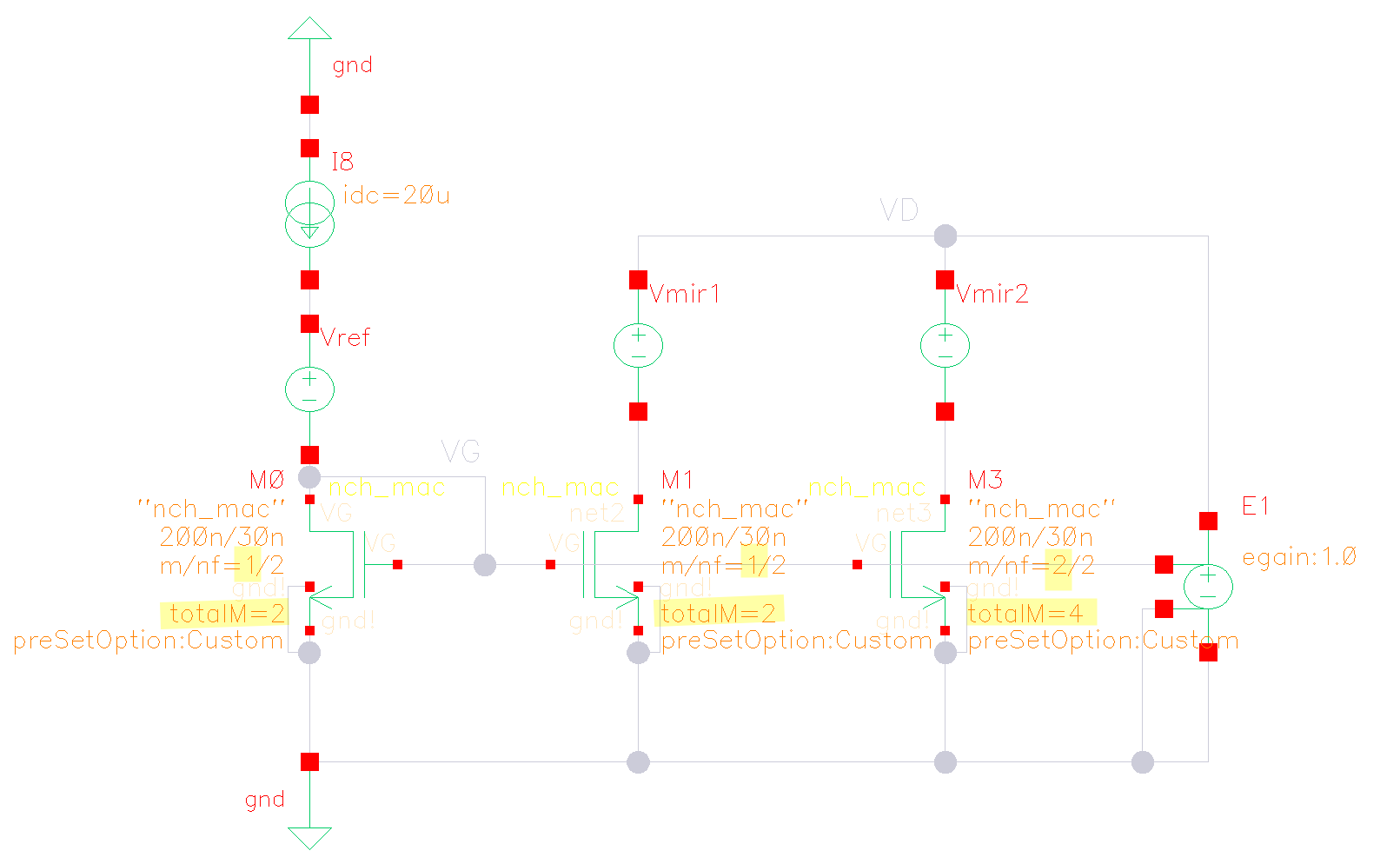
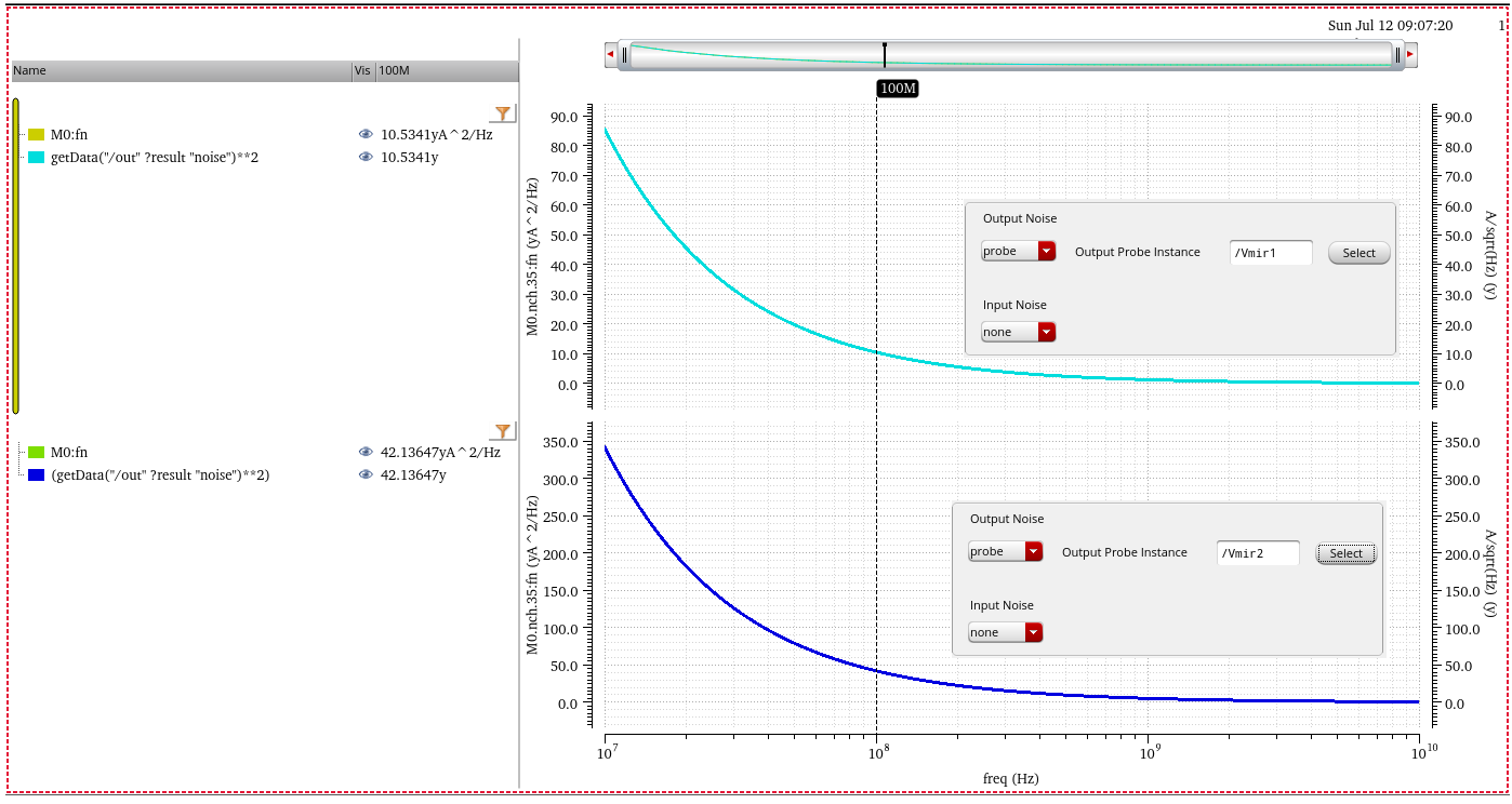
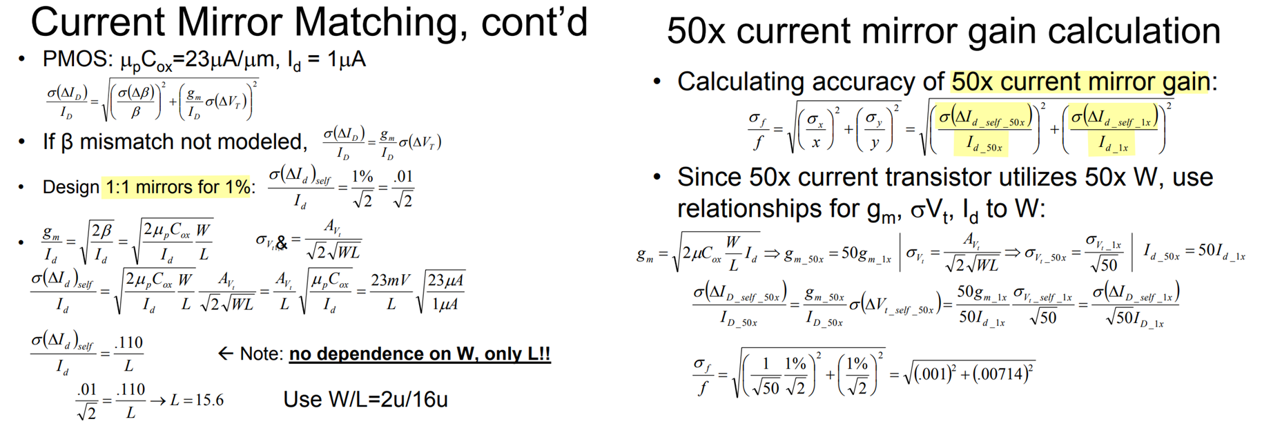
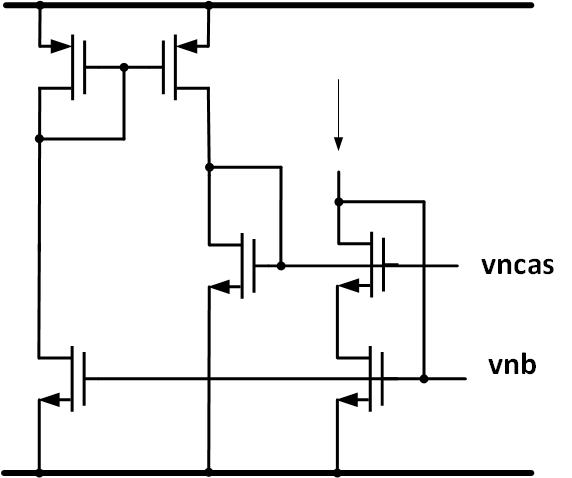
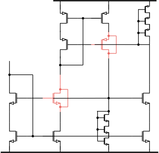
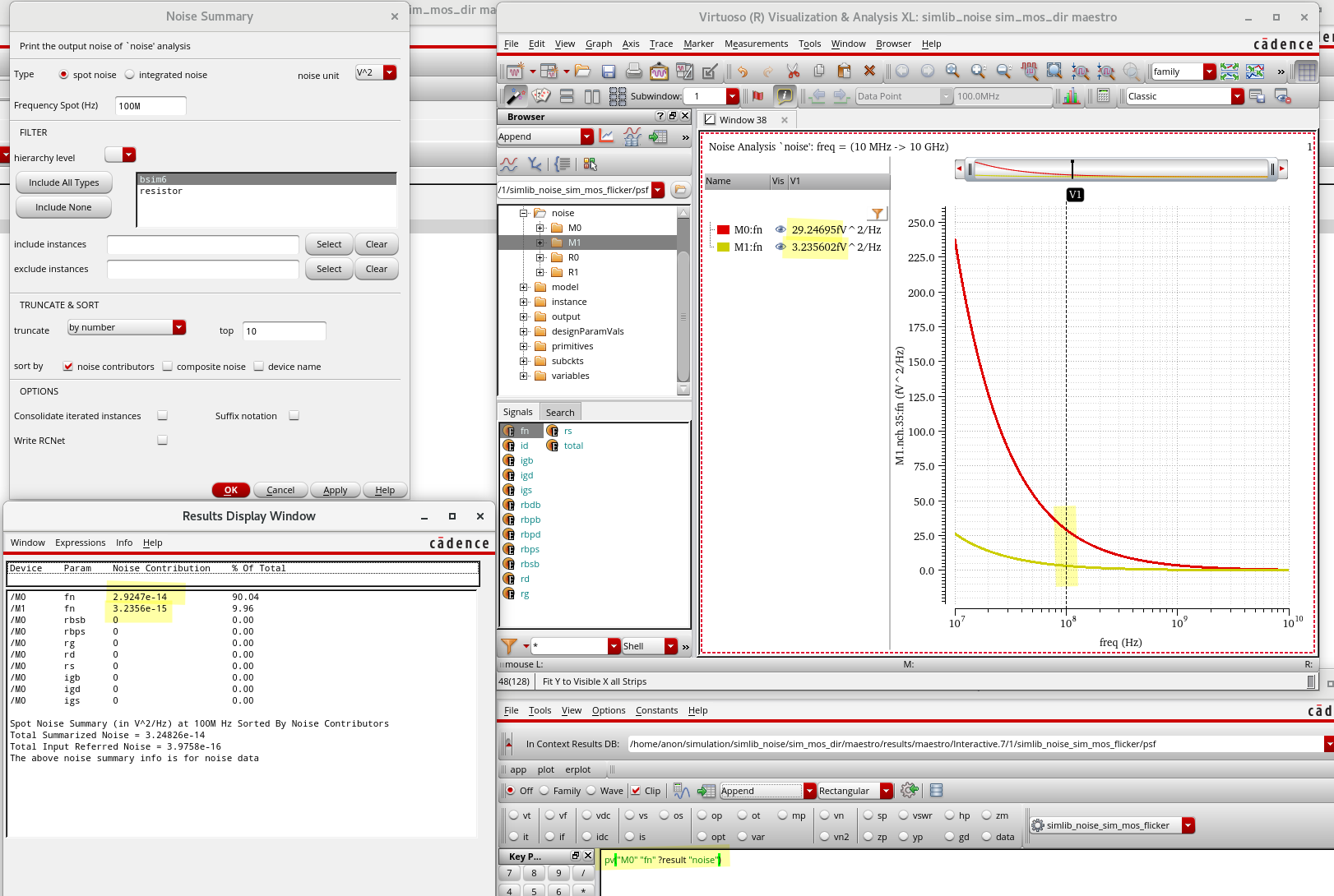
Noise of ref MOS is amplified by the current mirror's gain
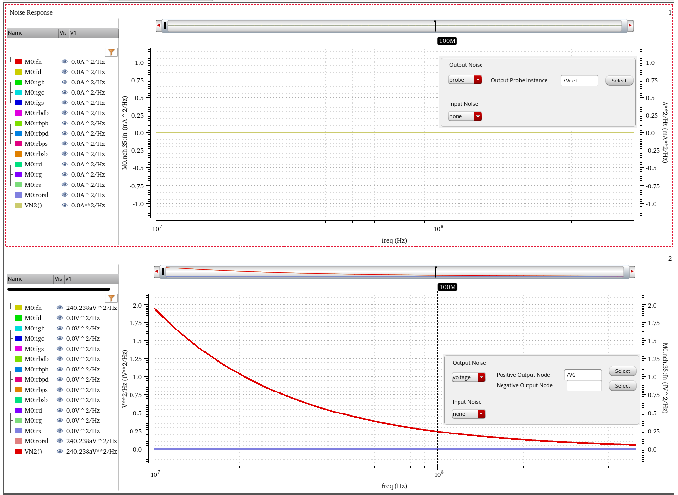
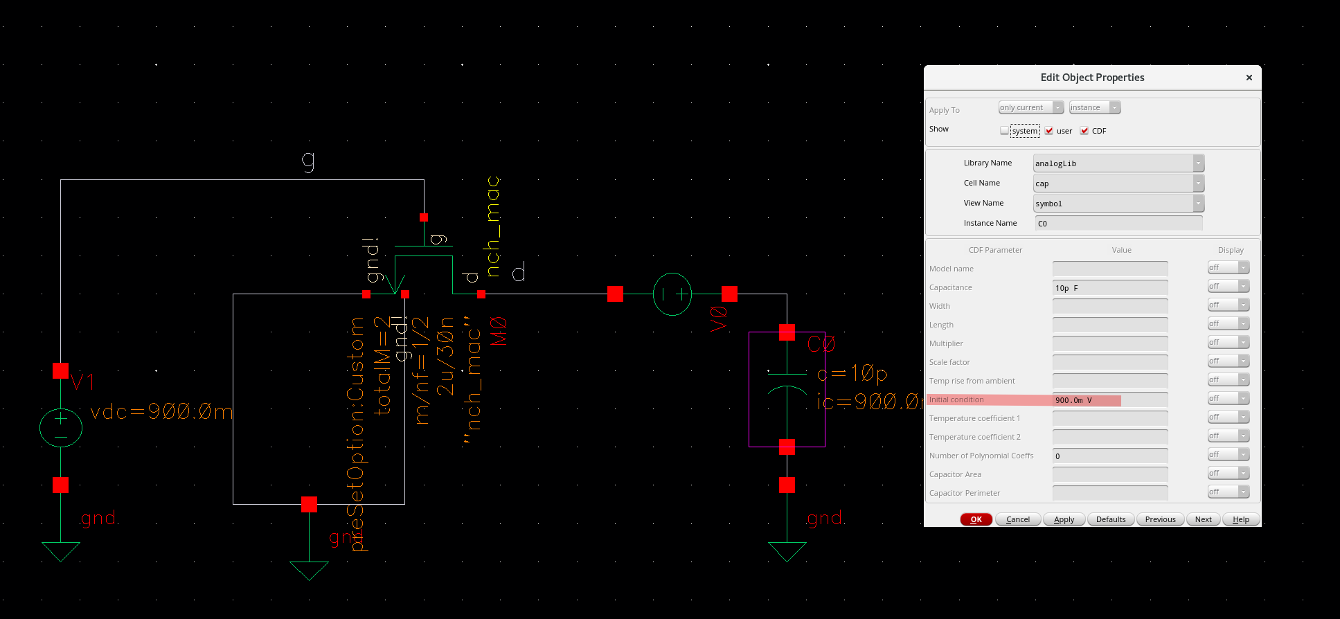
Due to M0 is biased by current source, we probe gate voltage instead
of current
result browser of instance show noise
contribution, which is same with noise summary
current mirror with source
follower
source follower alleviate gate leakage impact on reference
current
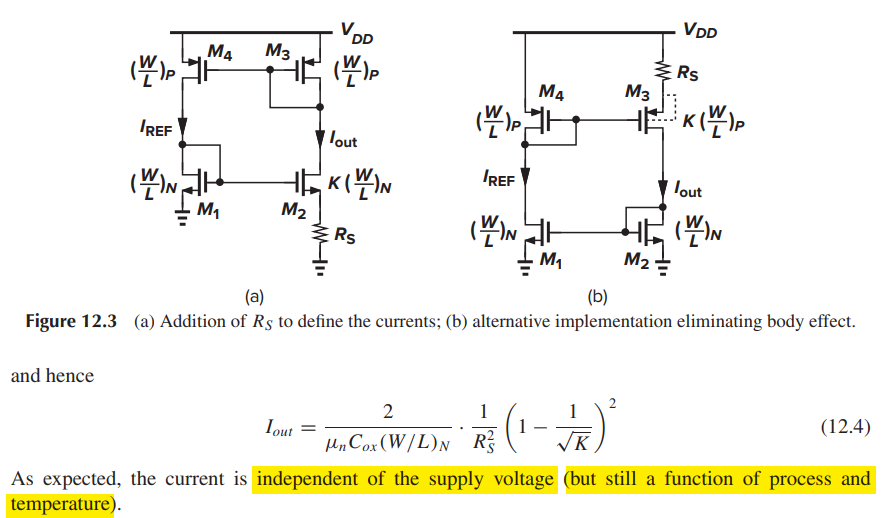
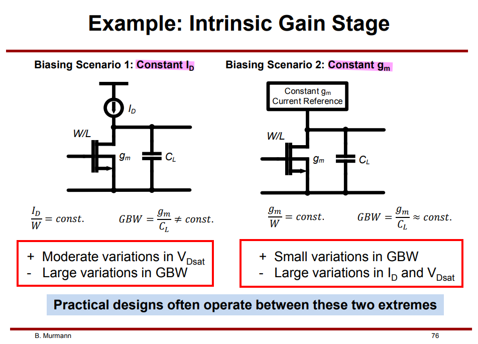
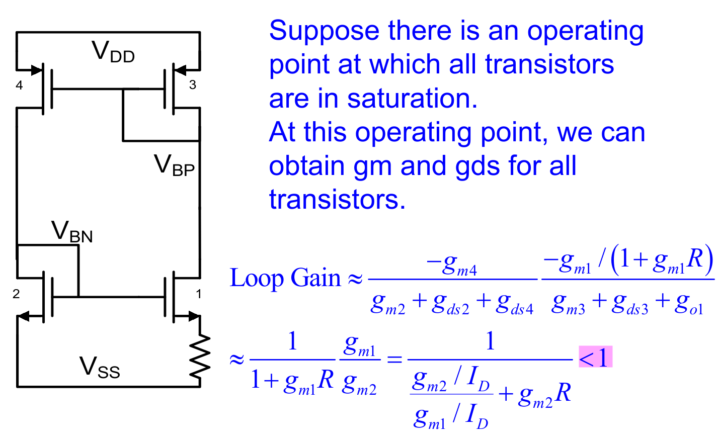
constant-gm
aka. Beta-multiplier reference
\(I_\text{out}\) is
PTAT in case temperature coefficient of \(R_s\) is less than that of \(\mu_n\)
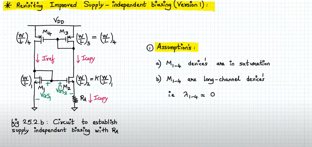
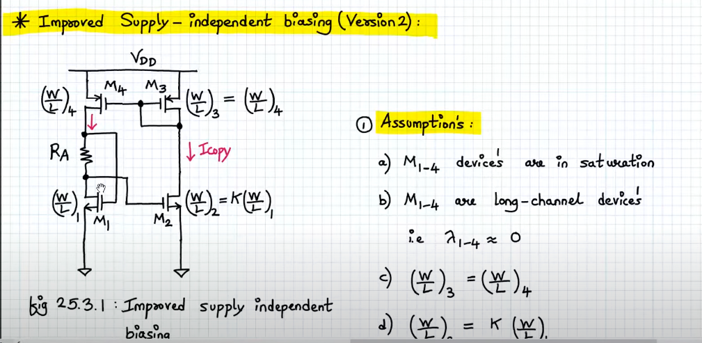
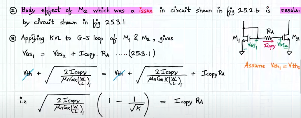
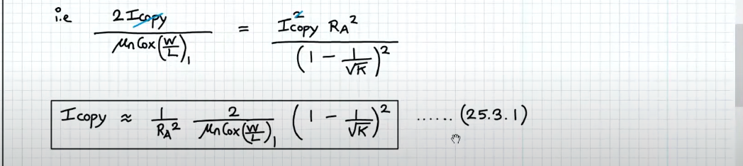
Body effect of M2
Boris Murmann, Systematic Design of Analog Circuits Using
Pre-Computed Lookup Tables
S. Pavan, "Systematic Development of CMOS Fixed-Transconductance Bias
Circuits," in IEEE Transactions on Circuits and Systems II: Express
Briefs, vol. 69, no. 5, pp. 2394-2397, May 2022
S. Pavan, "A Fixed Transconductance Bias Circuit for CMOS Analog
Integrated Circuits", IEEE International Symposium on Circuits and
Systems, ISCAS 2004, Vancouver , May 2004
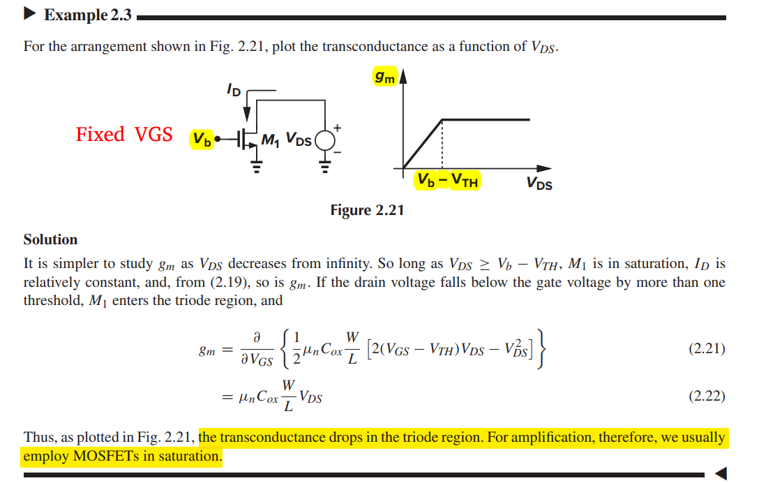
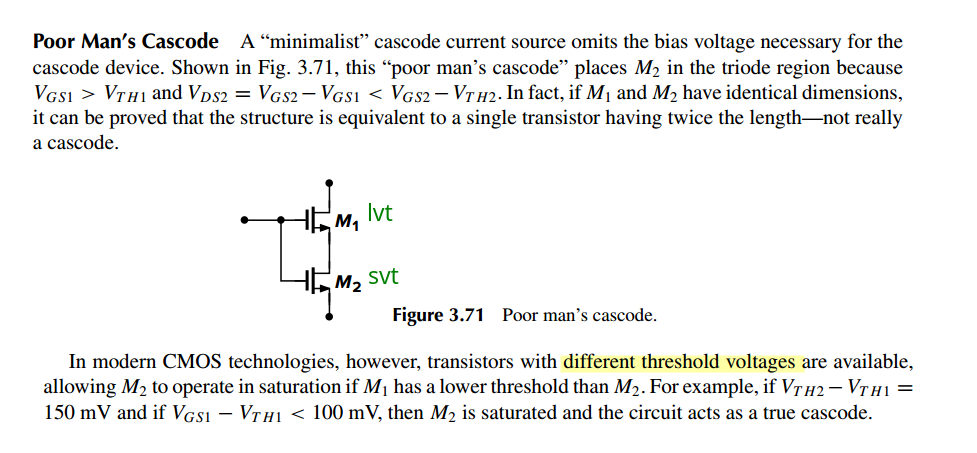
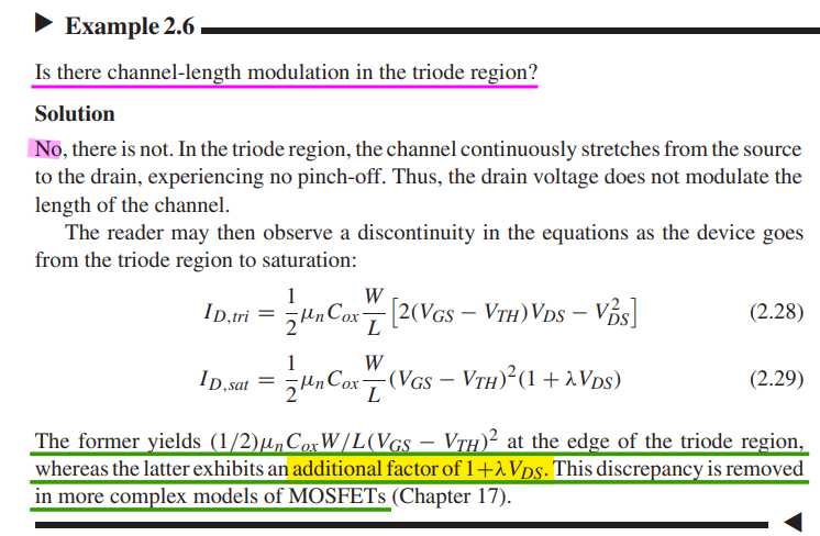
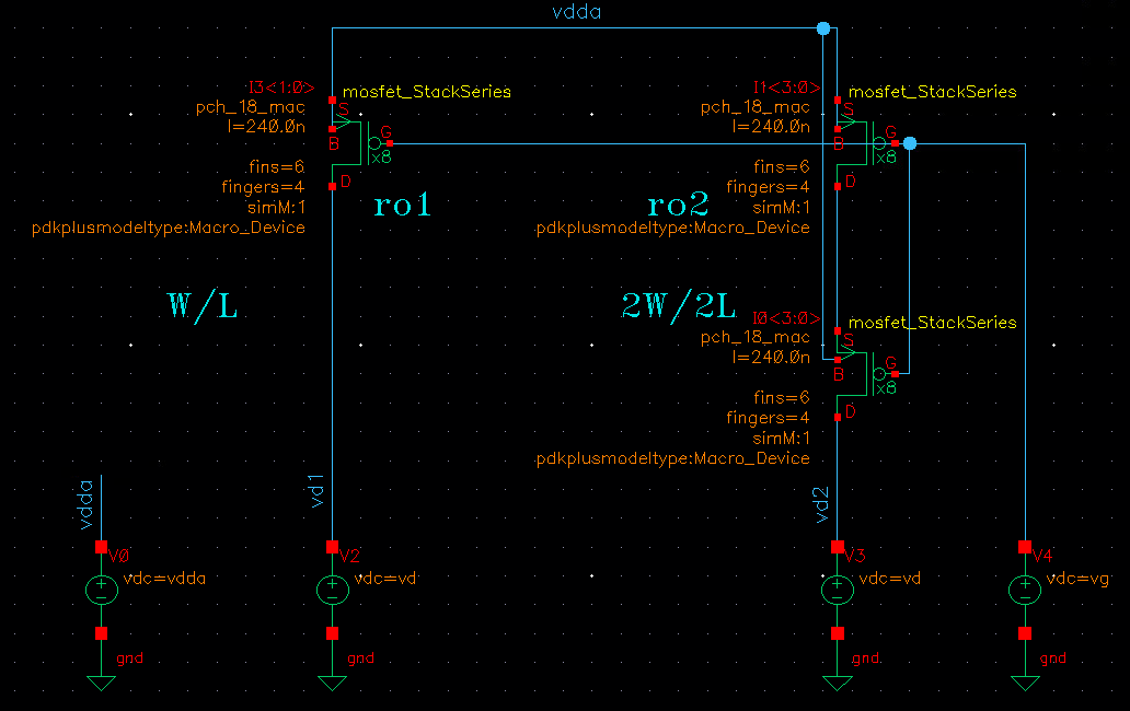
Why MOS in saturation ?
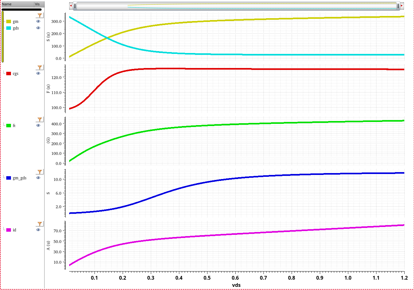
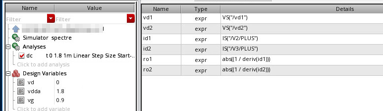
\(g_m\), \(g_\text{ds}\) at fixed \(V_\text{GS}\)
\(g_{ds}\) is constant in saturation
region
in triode region \[
g_{ds} = \mu_nC_{ox}\frac{W}{L}(V_{GS}-V_{TH}-V_{DS})
\]
Interestingly, \(g_m\) in the
saturation region is equal to the inverse of \(R_\text{on}\) in the deep triode
region.
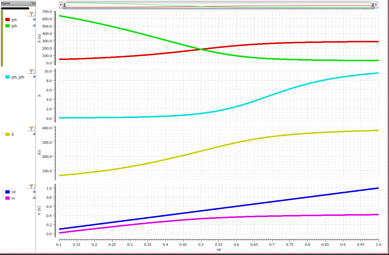
\(g_m\), \(g_\text{ds}\) at fixed \(I_d\), \(V_G\)
In triode region\[
I_D =
\frac{1}{2}\mu_nC_{ox}\frac{W}{L}[2(V_{GS}-V_{TH})V_{DS}-V_{DS}^2]
\] where \(I_D\) and \(V_G\) is fixed
Then \(V_S\) can be expressed with
\(V_D\), that is \[
V_S = V_{GT} - \sqrt{(V_{GT}-V_D)^2+V_{dsat}^2}
\] where \(V_{GT}=V_G-V_{TH}\),
\(V_{dsat}\) is \(V_{DS}\) saturation voltage \[
g_m =
\mu_nC_{ox}\frac{W}{L}\left(V_D-V_{GT}+\sqrt{(V_{GT}-V_D)^2+V_{dsat}^2}\right)
\] Then \[
\frac{\partial g_m}{\partial V_D} \propto 1 -
\frac{V_{GT}-V_D}{\sqrt{(V_{GT}-V_D)^2+V_{dsat}^2}} \gt 0
\]
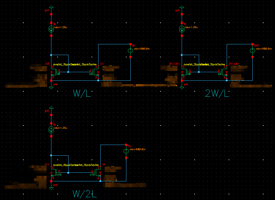
Another solution is to view the mirror branch as a
whole
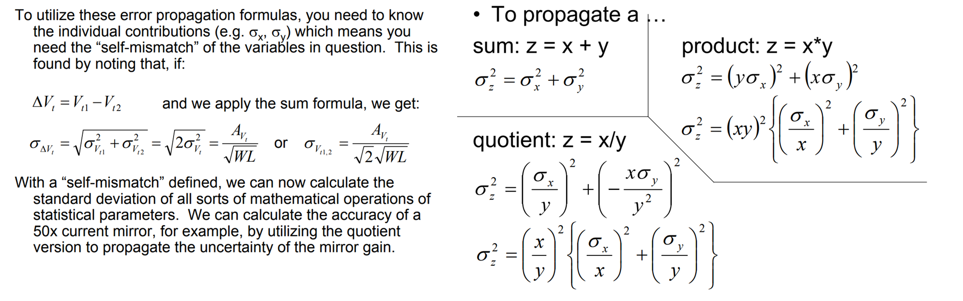
In source branch self mismatch \(\sigma_{vth,src} =
\frac{A_{vt}}{\sqrt{2WL}}\) and mirror branch self-mismatch \(\sigma_{vth,mir} =
\frac{A_{vt}}{\sqrt{2kWL}}\), then mutual mismatch is \[
\sigma_{vth} = \sqrt{\sigma_{vth,src}^2 + \sigma_{vth,mir}^2} =
\sigma_{vth,src}\sqrt{1+\frac{1}{k}}
\] mirror current variation \(\sigma_{I_k} = k g_m \sigma_{vth}\),
relative variation of mirror current is \[
\frac{\sigma_{I_k}}{I_k} = \frac{k g_m \sigma_{vth}}{kI} = \frac{g_m
\sigma_{vth,src}}{I}\sqrt{1+\frac{1}{k}}=\color{red}\frac{\sigma_{I}}{I}\sqrt{1+\frac{1}{k}}
\]
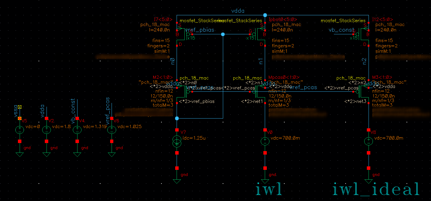
Biasing
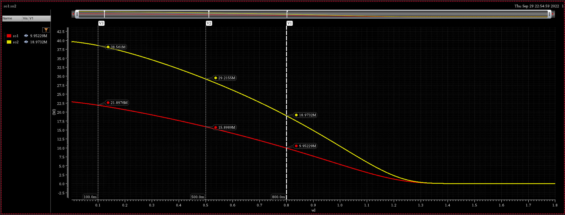
current source and global variation Monte Carlo
iwl: biased by mirror
iwl_ideal: biased by vdc source, whose
value is typical corner
For local variation, constant voltage bias
(vb_const in schematic) help reduce variation from \(\sqrt{2}\Delta V_{th}\) to \(\Delta V_{th}\)
For global variation, all device have same
variation, mirror help reduce variation by sharing same \(V_{gs}\)
global variation + local variation (All MC)
local variation (Mismatch MC)
global variation (Process MC)
We had better bias mos gate with mirror rather than the vdc
source while simulating sub-block.
This is real situation due to current source are always biased by
mirror and vdc biasing don't give the right result in global
variation Monte Carlo simulation (542.8n is too pessimistic,
13.07p is right result)
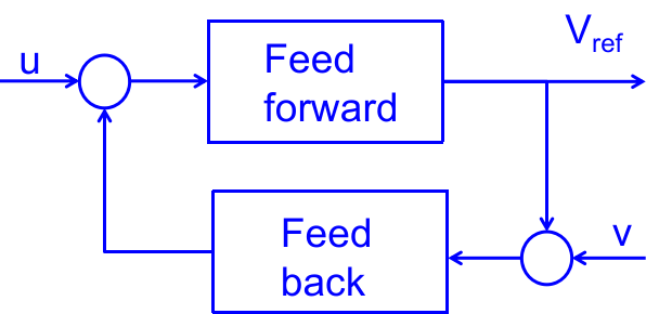
For any given constant values of u and v, the
constant values of variables that solve the the feed back relationship
are called the operating points, or equilibrium
points.
Operating points can be either stable or
unstable.
An operating point is unstable if any or some small perturbation near
it causes divergence away from that operating point.
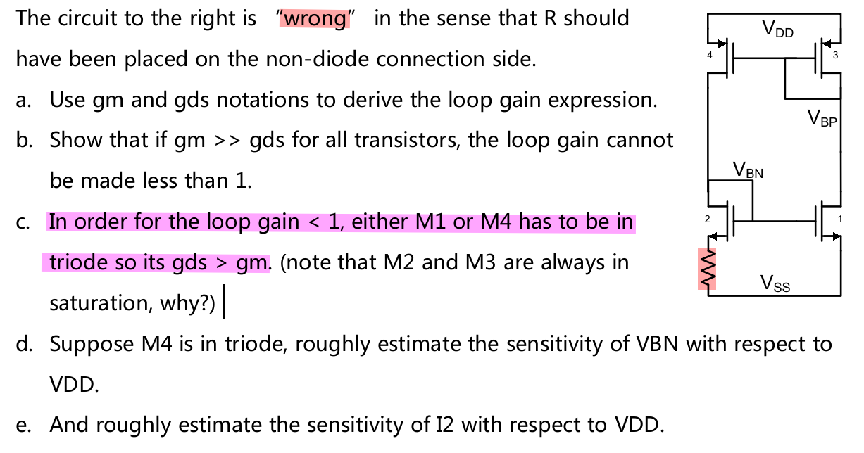
If the loop gain evaluated at an operating point is less than
one, that operating point is stable.
This is a sufficient condition
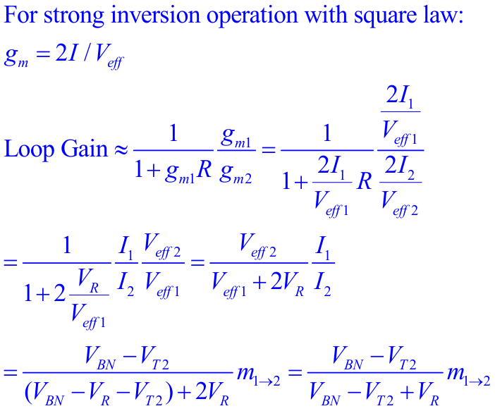
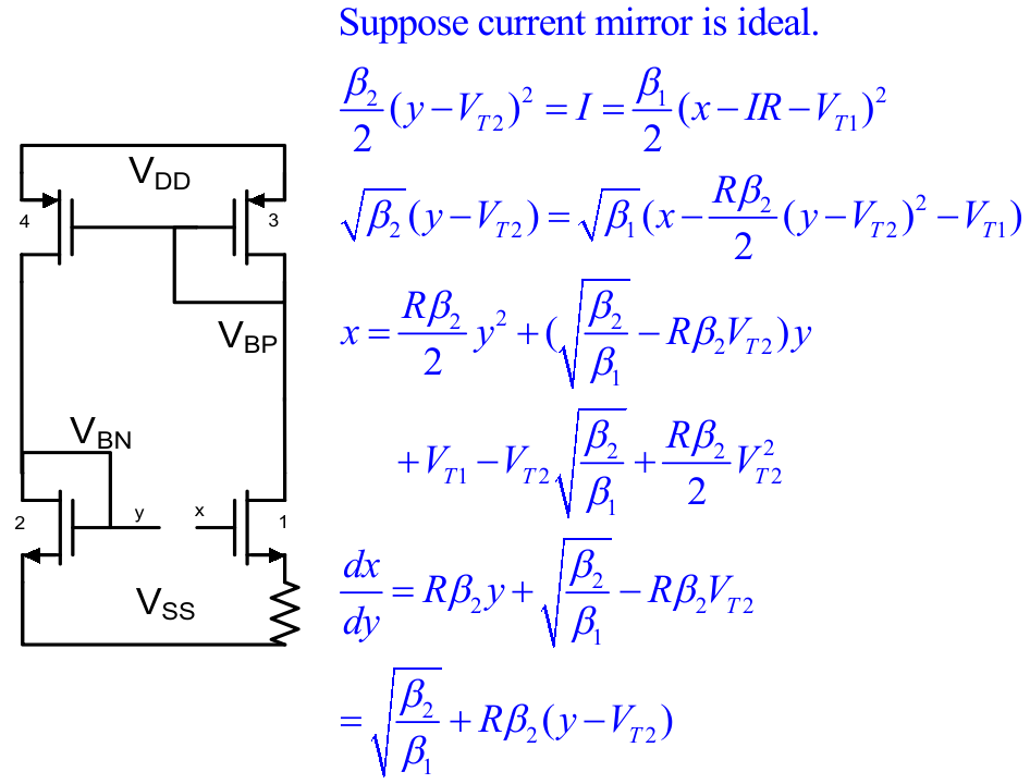
With \(m_{1\to 2} = 1\)\[
\text{Loop Gain} \simeq \frac{V_{BN}-V_{T2}}{V_{BN}-V_{T2} + V_R}
\tag{$LG_0$}
\] Assuming all MOS in strong inv operation, \(I\), \(V_{BN}\) and \(V_R\) is obtain \[\begin{align}
I &= \frac{2\beta _1 + 2\beta _2 - 4\sqrt{\beta _1 \beta
_2}}{R^2\beta _1 \beta _2} \\
V_{BN} &= V_{T2} + \frac{2}{R\beta _2}(1- \sqrt{\frac{\beta
_2}{\beta _1}}) \\
IR &= \frac{2}{R}\left( \frac{1}{\sqrt{\beta_2}}
- \frac{1}{\sqrt{\beta_1}} \right)
\end{align}\]
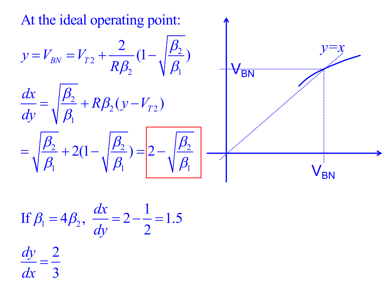
Substitute \(V_{BN}\) and \(V_R\) of \(LG_0\)\[\begin{align}
\text{Loop Gain} & \simeq
\frac{1-\sqrt{\frac{\beta_2}{\beta_1}}}{\frac{\beta_2}{\beta_1} -
3\sqrt{\frac{\beta_2}{\beta_1}}+2} \\
&= \frac{1}{2-\sqrt{\frac{\beta_2}{\beta_1}}} \tag{$LG_1$}
\end{align}\]
E. Alvarez-Fontecilla, P. S. Wilkins and S. C. Rose, "Understanding
High-Resolution Dynamic Element Matching DACs [Feature]," in IEEE
Circuits and Systems Magazine, vol. 23, no. 4, pp. 34-43,
Fourthquarter 2023
E. Alvarez-Fontecilla and P. S. Wilkins, "Linearity Through Democracy
[Feature]," in IEEE Circuits and Systems Magazine, vol. 25, no.
1, pp. 58-69, Firstquarter 2025
Autozeroing
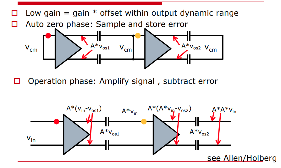
offset is sampled and then subtracted from the
input
Measure the offset somehow and then subtract it from the input
signal
then \[
\Delta I_1 = \frac{1}{2}(V_{a1} - V_{b1})(g_{m,a1}+g_{m,b1})
\] That is, \(g_{m,a1}+g_{m,b1} = \mu
C_{OX}\frac{W}{L}(V_{a1}+V_{b1} - 2V_{TH})\)
To minimize the difference between \(\Delta
I_1\) and \(\Delta I_0\), the
drift of both differential and common mode between \(V_a\) and \(V_b\) shall be alleviated
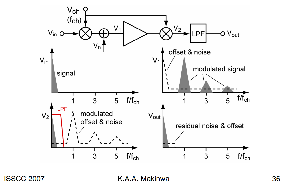
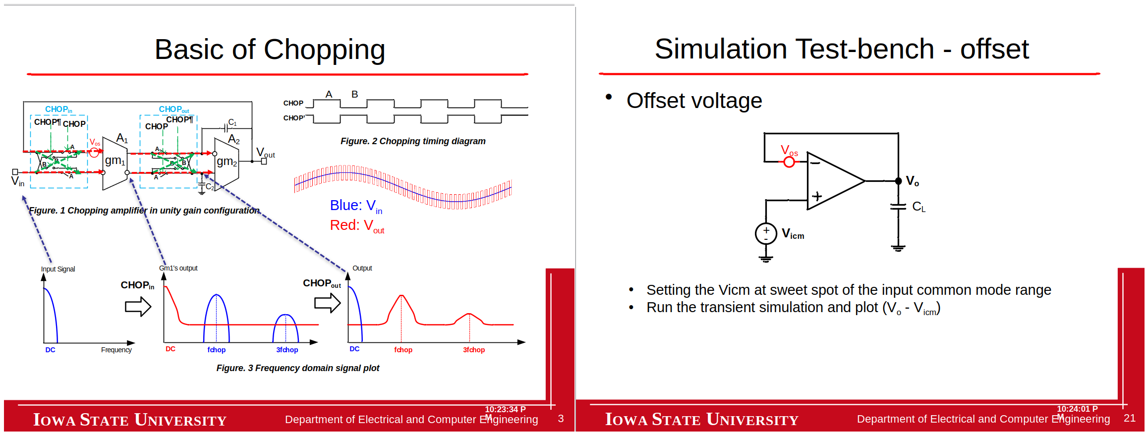
Chopping
offset is modulated away from the signal band and
then filtered out
Modulate the offset away from DC and then filter it out
Good: Magically reduces offset, 1/f noise, drift
Bad: But creates switching spikes, chopper ripple
and other artifacts …
Chopping in the Frequency
Domain
Square-wave Modulation
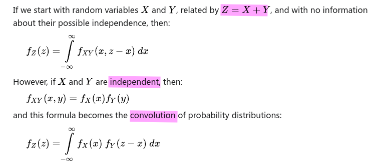
definition of convolution \(y(t) =
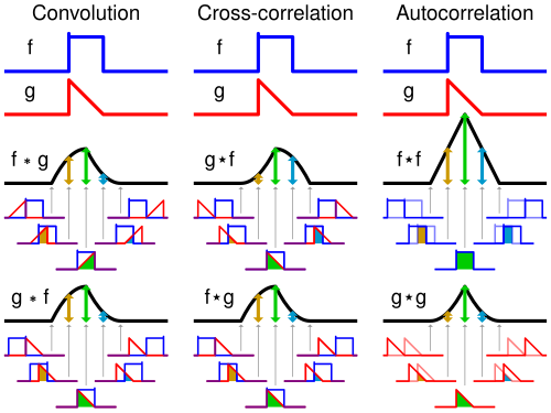
x(t)*h(t)= \int_{-\infty}^{\infty} x(\tau)h(t-\tau)d\tau\)
The Fourier transform of \(s(t)=x(t)x(t)\), and we know \[\begin{align}
S(j2n\omega_0) &= \frac{1}{2\pi}\int X(j(2n\omega_0
-\omega))X(j\omega) d\omega\\
&= \frac{1}{2\pi}\int X(j(\omega-2n\omega_0))X(j\omega) d\omega
\end{align}\]
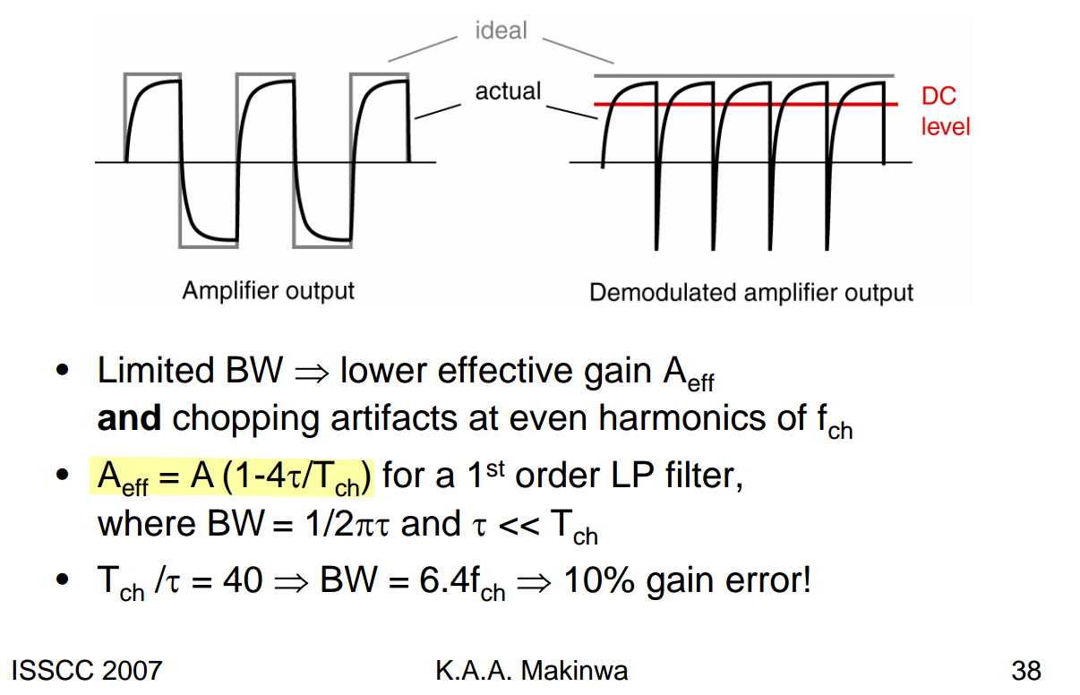
lower effective gain: DC level at the output of the
amplifiers is a bit less than what it should be
chopping artifacts at the even harmonics: frequency of
output is \(2f_{ch}\)
Below we justify \(A_\text{eff} =
A(1-4\tau/T_\text{ch})\)\[
V_o(t) = A + (V_0-A)e^{-t/\tau} \qquad V_o(T/2) = -V_0
\]
then \[
V_0 = -A\frac{1-e^{-T/2\tau}}{1+e^{-T/2\tau}}
\] Then DC level is \[
A_\text{eff} = \frac{1}{T/2}\int_0^{T/2} V_o(t)dt =
A\left(1-\frac{4\tau}{T}\cdot
\frac{1-e^{-T/2\tau}}{1+e^{-T/2\tau}}\right)\approx
A\left(1-\frac{4\tau}{T}\right)
\]
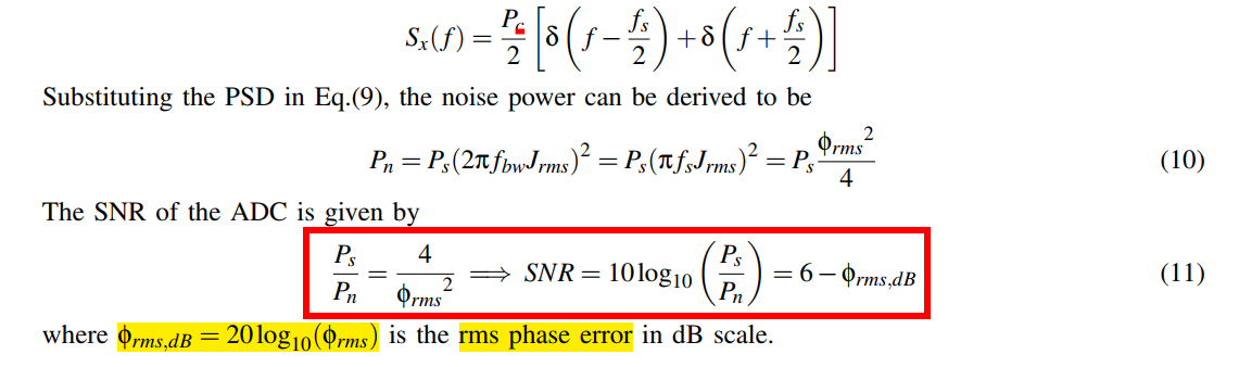
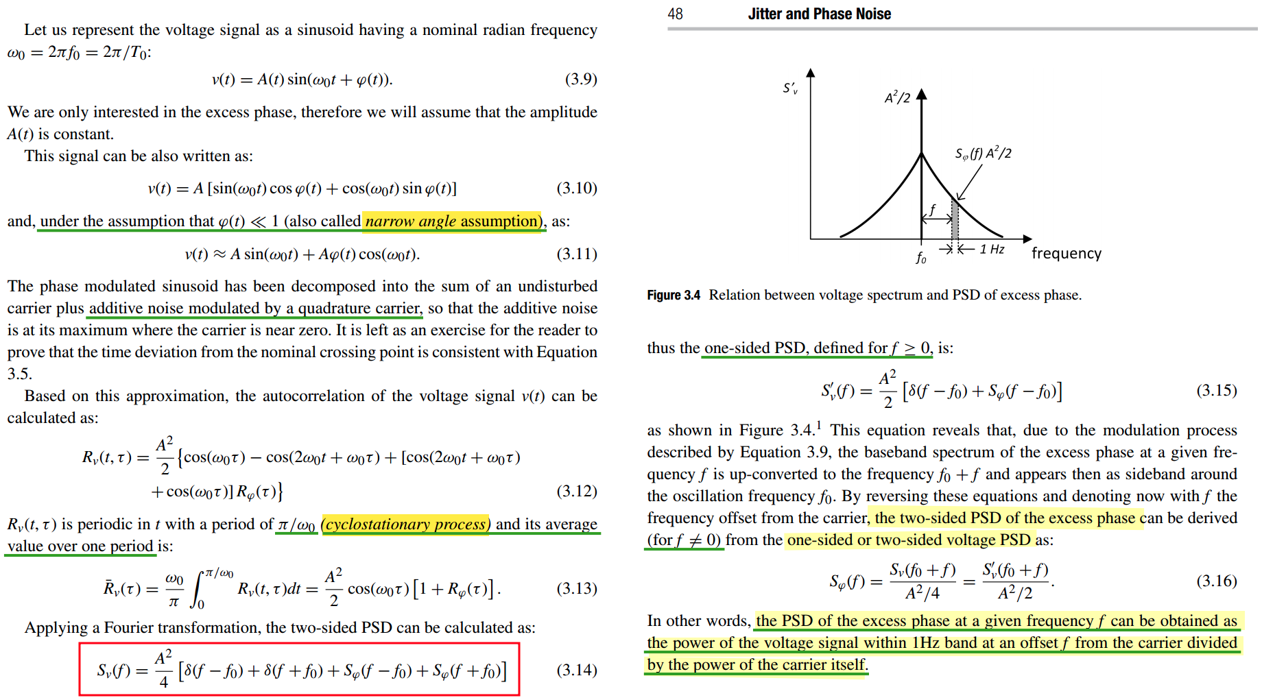
Nicola Da Dalt , Understanding Jitter and Phase Noise: 3.1.3 Voltage
to Excess Phase Transformations: Random Noise
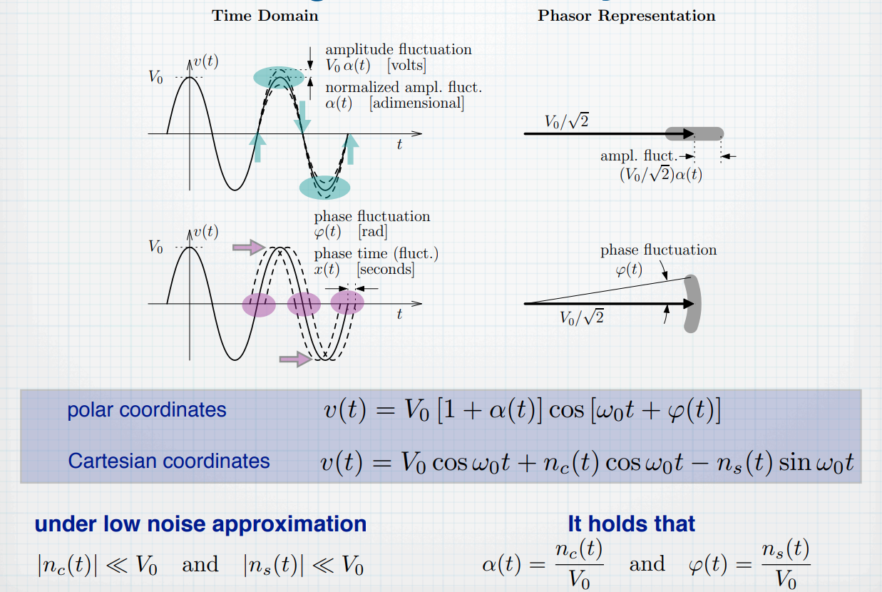
Given \(\color{blue}\phi(t)\ll 1\),
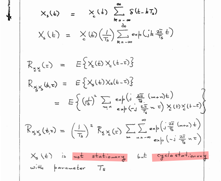
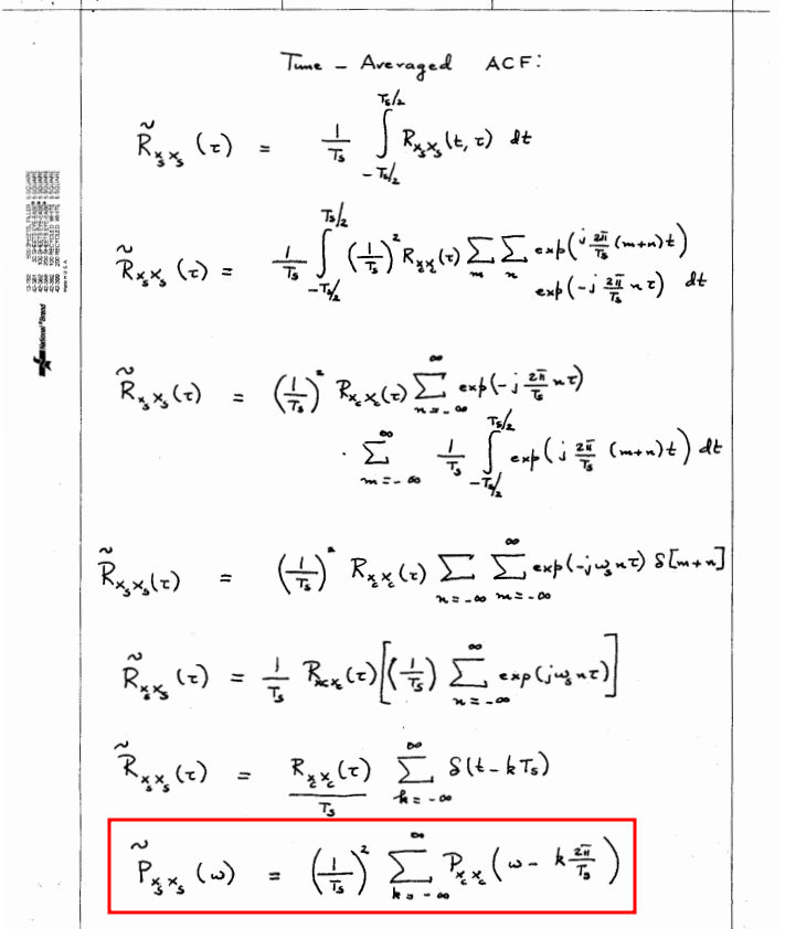
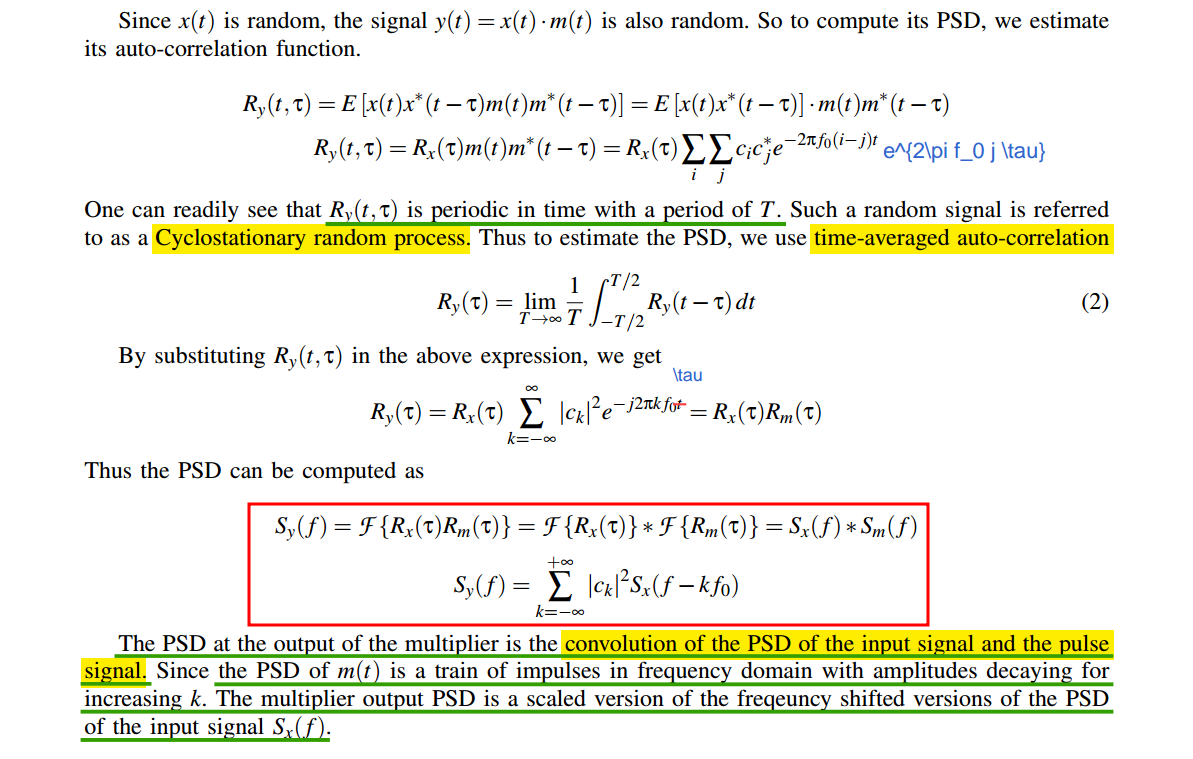
the autocorrelation still depends on absolute time \(t\). Therefore \(v(t)\) is cyclostationary,
and they must take a time average over one carrier
period.
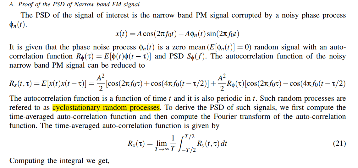
Chembiyan T. Jitter and Phase Noise in Phase Locked Loops [link]
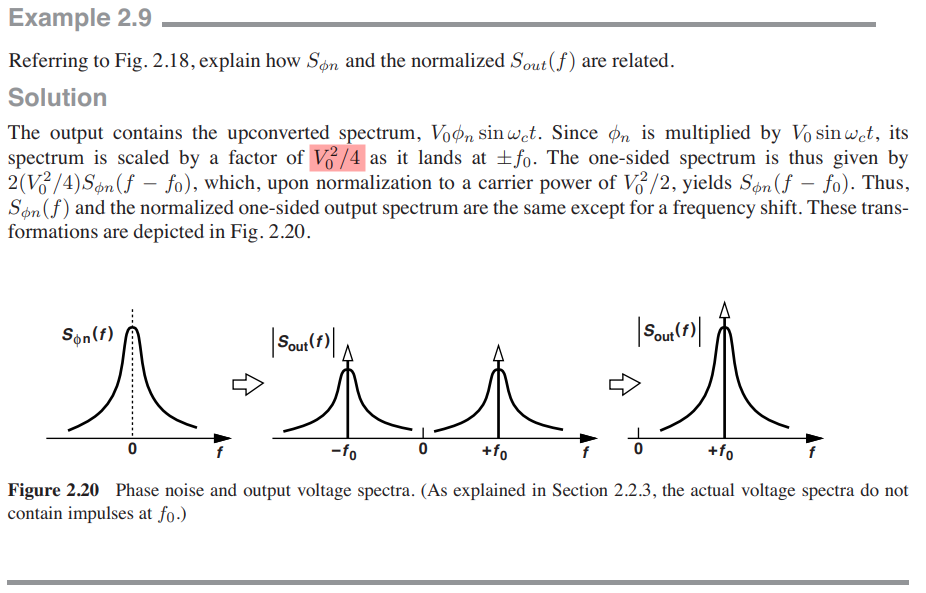
\[
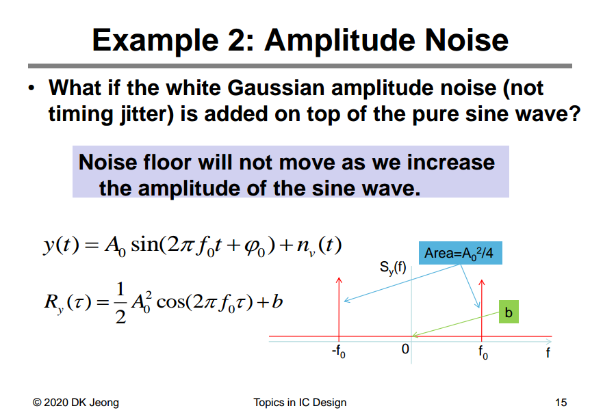
y(t) = A\cos(2\pi f_0t+\phi_n(t)) \approx A \cos(2\pi f_0 t) - A \phi_n
(t)\sin(2\pi f_0 t)
\]
\[
R_x(\tau) = \frac{A^2}{2}\cos(2\pi f_0\tau)
+ \frac{A^2}{2}R_\phi(\tau)\cos(2\pi f_0\tau)
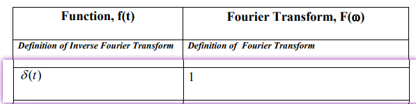
\] The PSD of the signal \(x(t)\) is given by \[
S_x(f) = \mathcal{F}\{R_x(\tau)\} =
\frac{P_c}{2}\left[\delta(f+f_0)+\delta(f-f_0)+S_\phi(f+f_0)+S_\phi(f-f_0)\right]
\] where \(P_c = A^2/2\) is the
carrier power of the signal
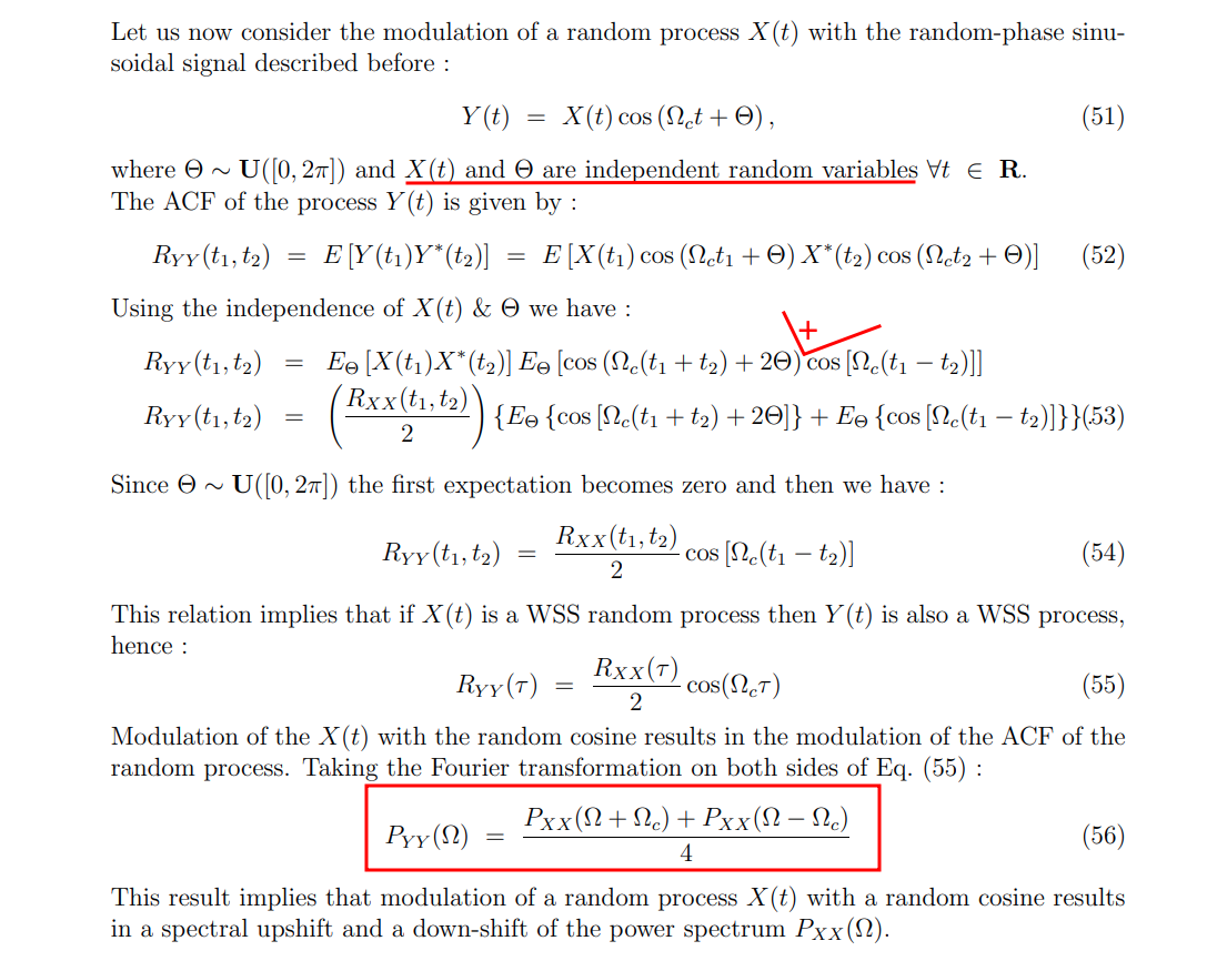
modulated with full-cycle
random
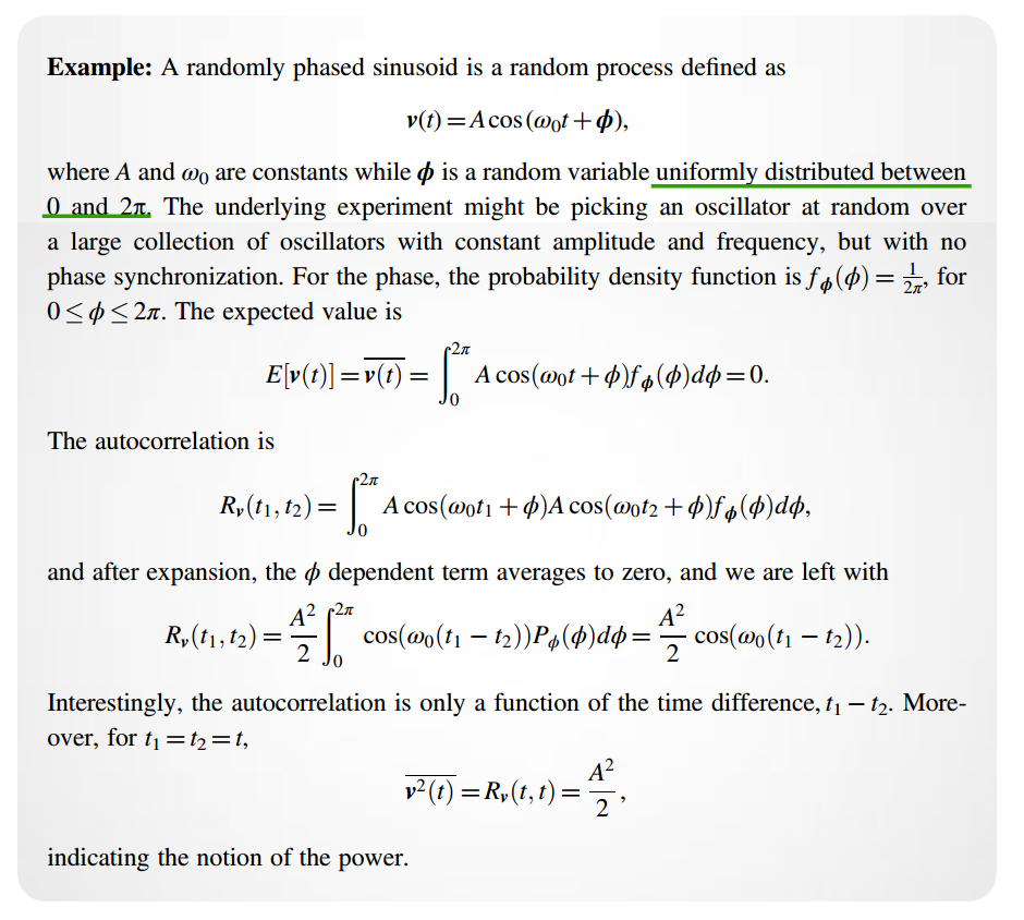
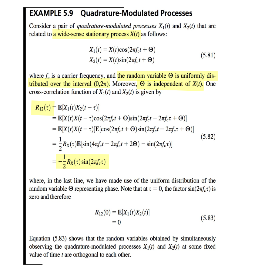
Given \(\color{blue}\Theta\sim
U[0,2\pi]\), after ensemble averaging, the autocorrelation
becomes WSS
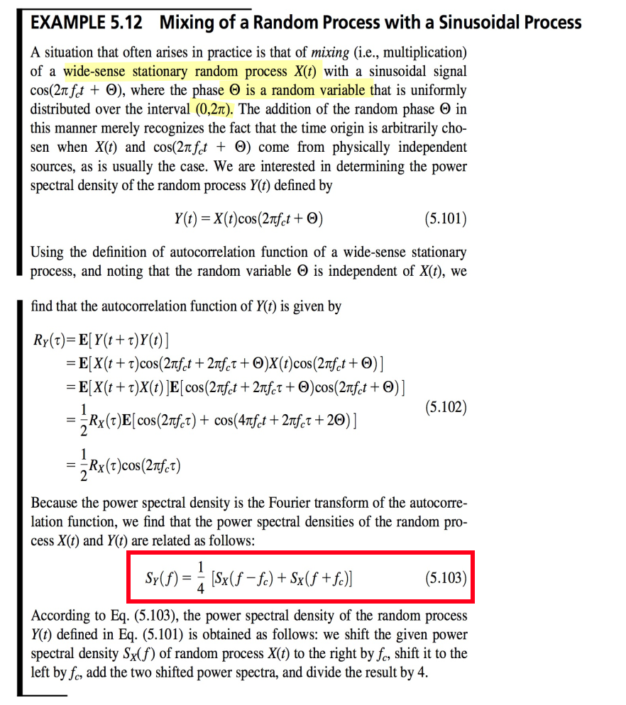
Haykin, Simon S., and Michael Moher. Communication Systems.
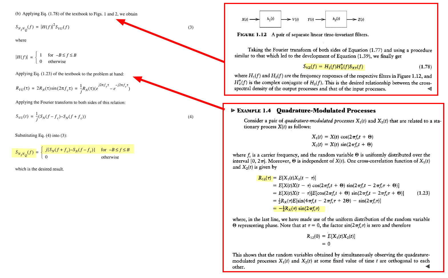
5th ed. John Wiley & Sons, 2009. - Mixing of a Random Process
with a Sinusoidal Process
Assume \(\Theta\sim \mathcal
U[0,2\pi)\) is a single random phase that remains
constant for all \(t\): \[
\color{blue}\boxed{X(t)=A\cos(\omega_0t+\Theta).}
\]
For \(t_1\) and \(t_2\), \[
R_X(t_1,t_2)
=
\mathbb E[X(t_1)X(t_2)].
\] Using \(\cos a\cos
b=\frac{1}{2}\left[\cos(a-b)+\cos(a+b)\right],\)
we obtain \[
\begin{aligned}
R_X(t_1,t_2)
&=
\frac{A^2}{2}
\mathbb E\left[
\cos\big(\omega_0(t_1-t_2)\big)
+
\cos\big(\omega_0(t_1+t_2)+2\Theta\big)
\right].
\end{aligned}
\] Since \(\Theta\) is uniform,
\[
\mathbb E\left[
\cos\big(\omega_0(t_1+t_2)+2\Theta\big)
\right]=0.
\] Therefore, \[
\boxed{
R_X(t_1,t_2)
=
\frac{A^2}{2}
\cos\big(\omega_0(t_1-t_2)\big)
}
\] or, defining \(\tau=t_1-t_2\), \[
\boxed{
R_X(\tau)=\frac{A^2}{2}\cos(\omega_0\tau)
}.
\] The autocorrelation depends only on the time difference \(\tau\).
Is it WSS?
Yes. The two WSS conditions are satisfied: \[
m_X(t)=0,
\] which is constant, and \[
R_X(t_1,t_2)=R_X(t_1-t_2).
\] Thus, \[
\boxed{X(t)\text{ is wide-sense stationary.}}
\] In fact, because a time shift simply changes the uniformly
distributed phase, \[
X(t+t_0)
=
A\cos\left(\omega_0t+\underbrace{\Theta+\omega_0t_0}_{\text{still
uniform modulo }2\pi}\right),
\] the process is also strict-sense
stationary.
Power spectral density
Using the angular-frequency Fourier-transform convention \[
S_X(\omega)
=
\int_{-\infty}^{\infty}
R_X(\tau)e^{-j\omega\tau}\,d\tau,
\] and \[
\mathcal F\{\cos(\omega_0\tau)\}
=
\pi\left[
\delta(\omega-\omega_0)+\delta(\omega+\omega_0)
\right],
\] we get \[
\boxed{
S_X(\omega)
=
\frac{\pi A^2}{2}
\left[
\delta(\omega-\omega_0)
+
\delta(\omega+\omega_0)
\right]
}.
\] Thus, the PSD consists of two spectral lines at \(\omega=\pm\omega_0\).
The total average power is \[
R_X(0)=\frac{A^2}{2},
\] and equivalently, \[
\frac{1}{2\pi}\int_{-\infty}^{\infty}S_X(\omega)\,d\omega
=
\frac{A^2}{2}.
\] For frequency \(f\), where
\(f_0=\omega_0/(2\pi)\), \[
\color{blue}\boxed{
S_X(f)
=
\frac{A^2}{4}
\left[
\delta(f-f_0)+\delta(f+f_0)
\right]
}.
\] The random phase makes the ensemble
stationary; a sinusoid with a fixed deterministic phase is not
normally regarded as a stationary random process because it contains no
random ensemble.
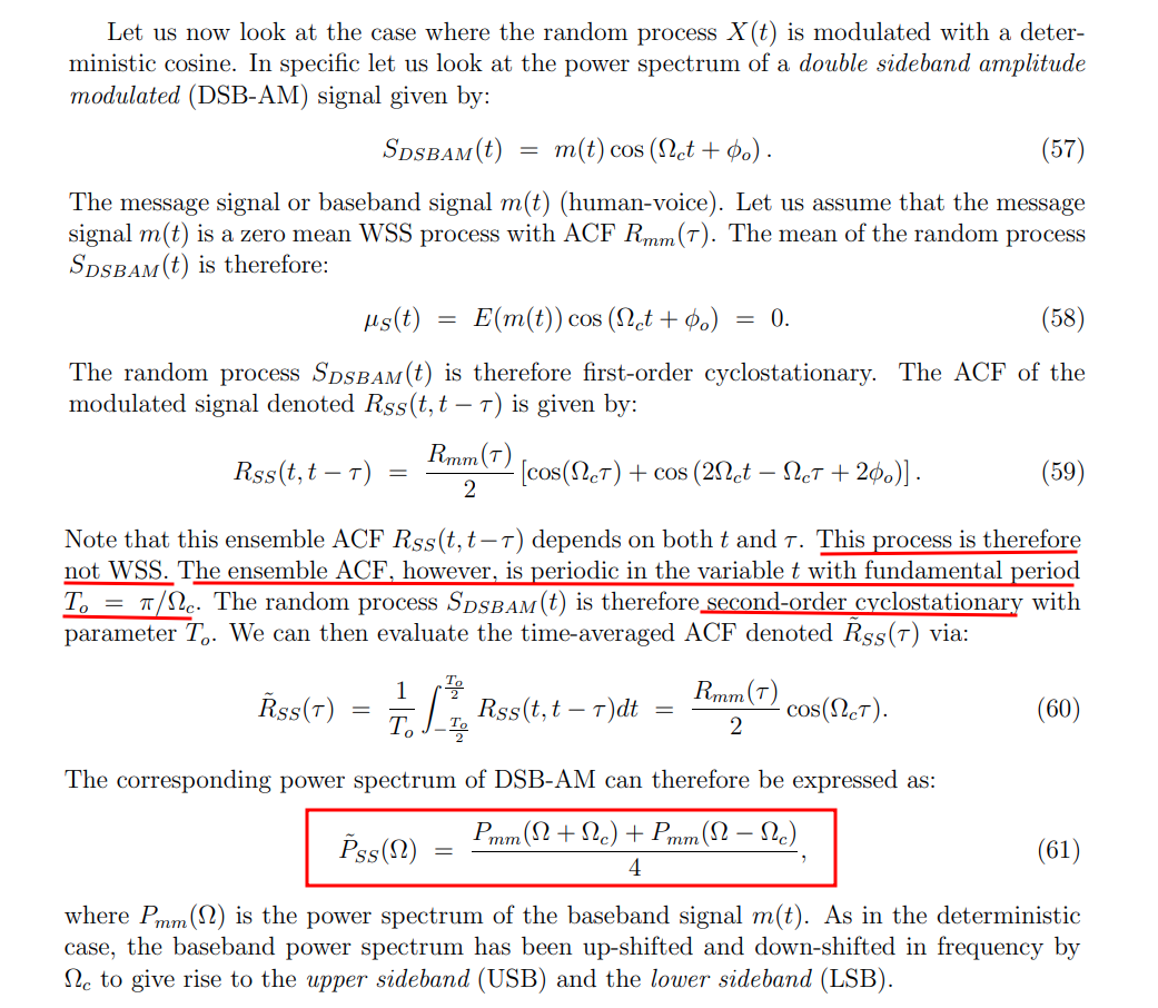
modulated with
deterministic cosine
the carrier phase/time origin is fixed, not randomized, it not WSS
but cyclostationary
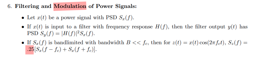
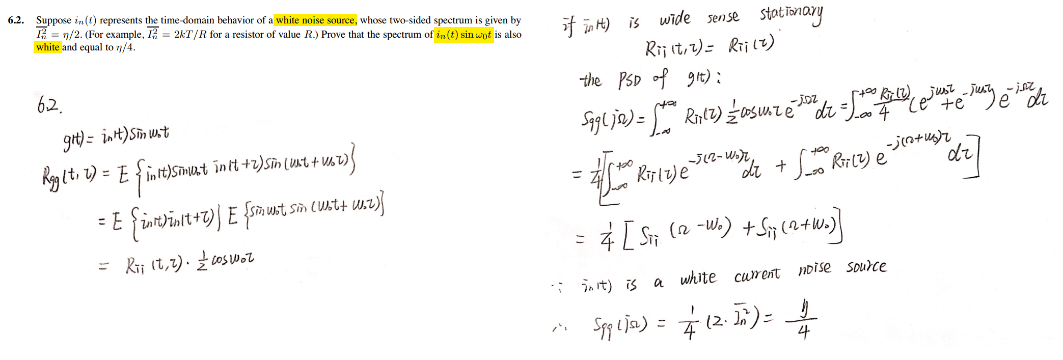
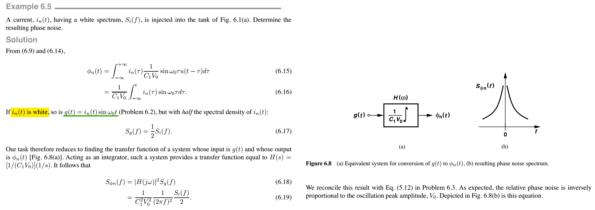
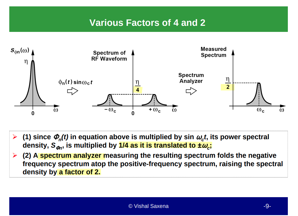
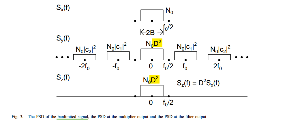
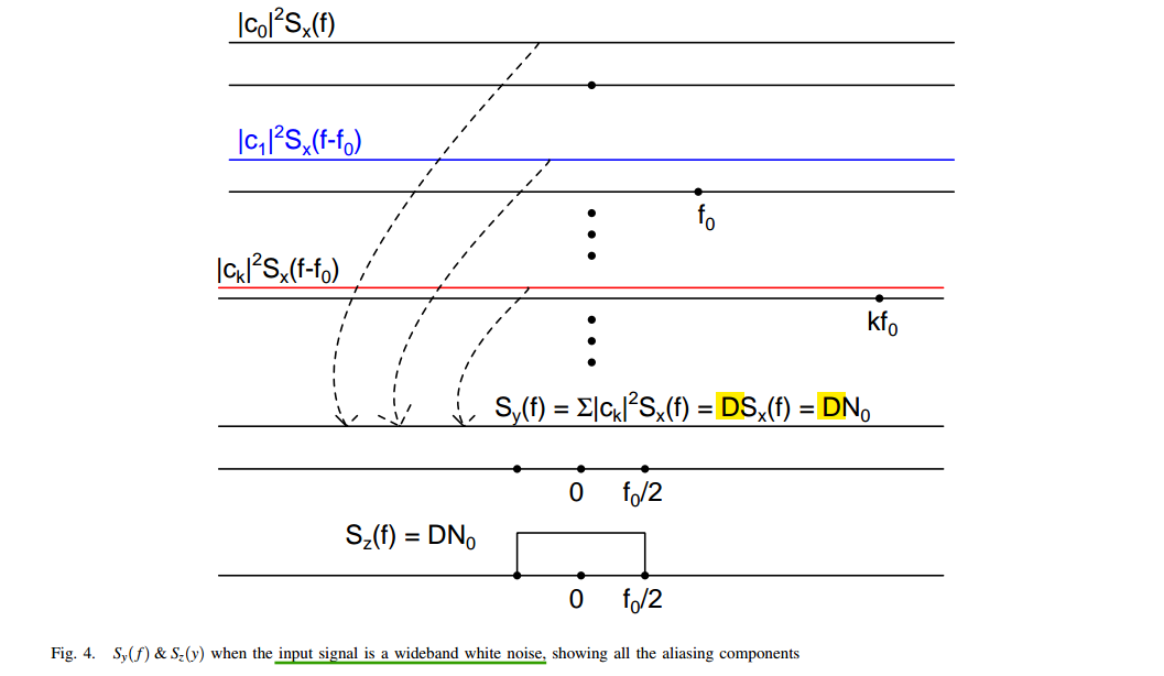
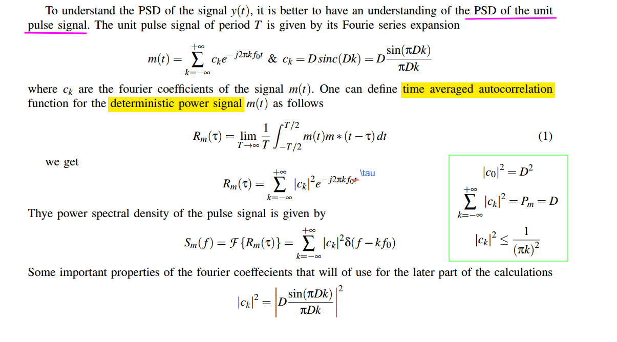
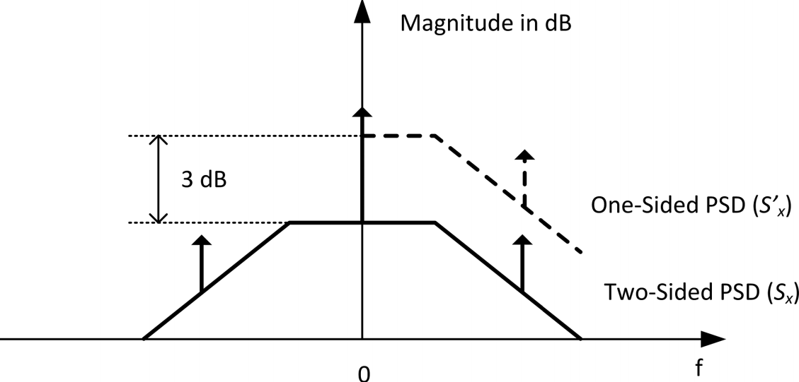
Thus an important result is: multiplying ideal white noise by
a sinusoid does not change the shape of its time-averaged PSD—it remains
white—but its average PSD is reduced by a factor of 2,
because
\[
\overline{\cos^2(\omega_0t)}=\frac12
\]
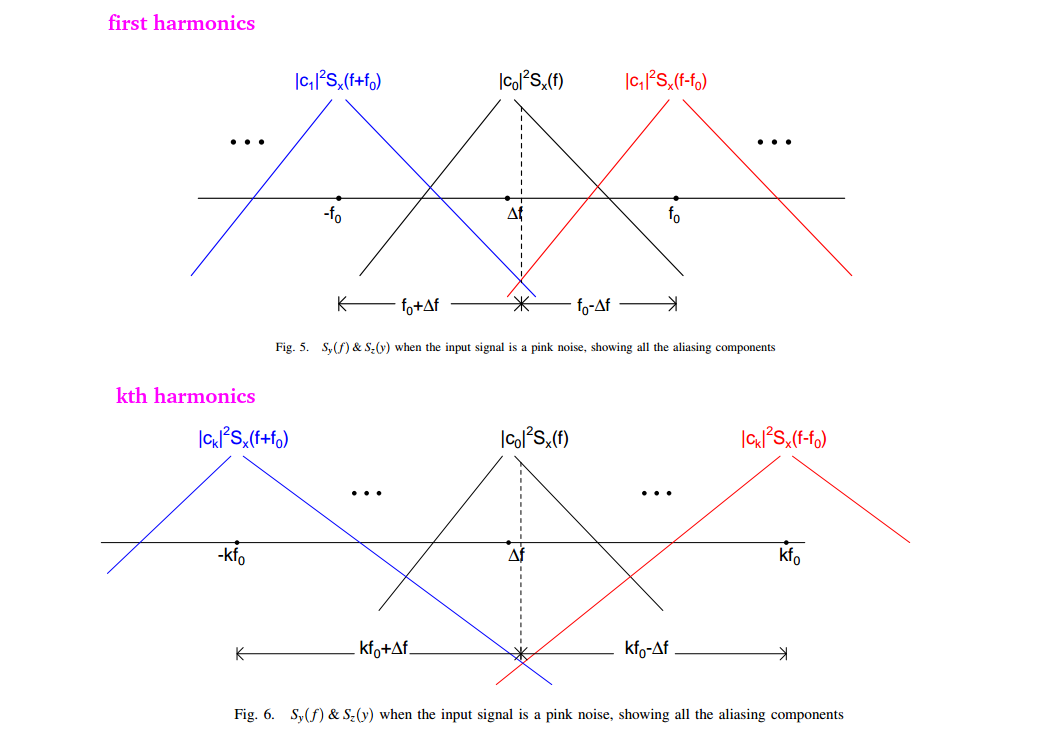
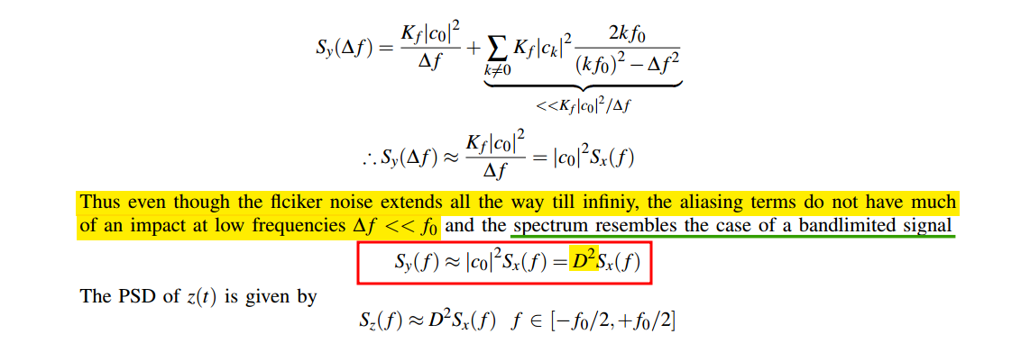
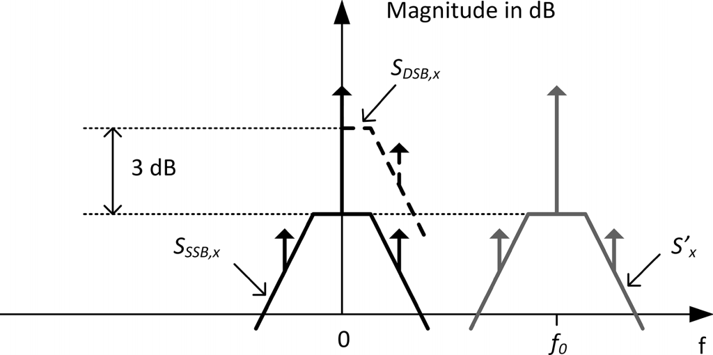
For colored noise, however, the sinusoidal multiplication creates two
shifted copies:
Alan V Oppenheim, Ronald W. Schafer. Discrete-Time Signal Processing,
3rd edition [pdf]
R. E. Ziemer and W. H. Tranter, Principles of Communications, 7th
ed., Wiley, 2013 [pdf]
John G. Proakis and Masoud Salehi, Fundamentals of communication
systems 2nd ed [pdf]
Rhee, W. and Yu, Z., 2024. Phase-Locked Loops: System
Perspectives and Circuit Design Aspects. John Wiley & Sons
Lacaita, Andrea Leonardo, Salvatore Levantino, and Carlo Samori.
Integrated frequency synthesizers for wireless systems.
Cambridge University Press, 2007
Phillips, Joel R. and Kenneth S. Kundert. "Noise in mixers,
oscillators, samplers, and logic: an introduction to cyclostationary
noise." Proceedings of the IEEE 2000 Custom Integrated Circuits
Conference. [pdf, slides]
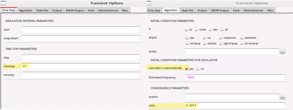
cmin is a small artificial capacitance that the
simulator adds from every circuit node to ground during
transient simulation. Cadence recommends it mainly as a convergence aid
because it smooths abrupt/discontinuous behavior that can force
extremely small timesteps
This is not a physical capacitor in your schematic.
It is a numerical stabilization parameter.
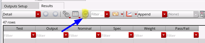
undo sorting in ADE
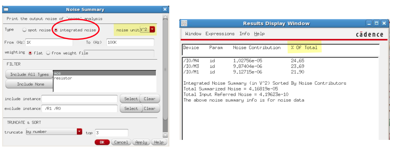
Noise Analysis
The % / Total column in the noise summary table always
displays values in \(V^{2}\)
contribution, regardless of whether noise unit option is
set to V or V^2
result browser of instance show noise
contribution, which is same with noise summary
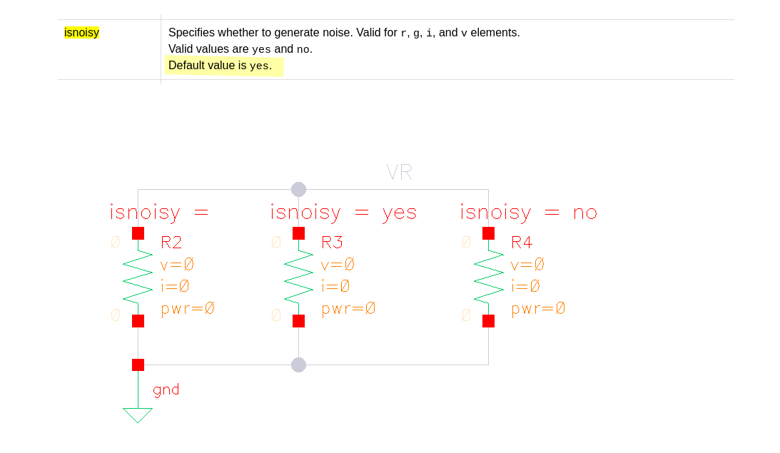
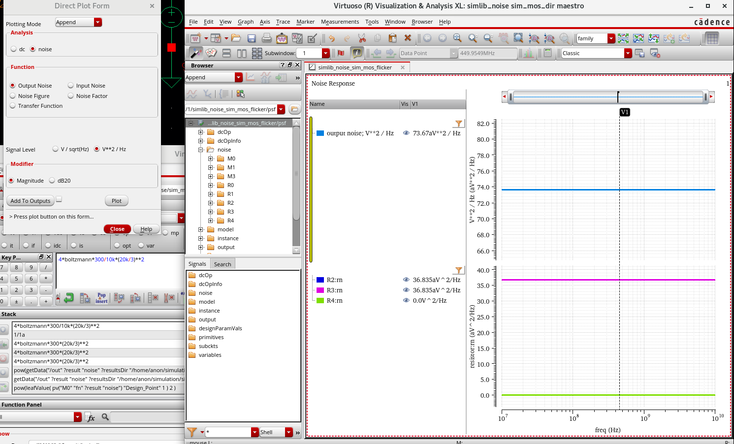
res isnoisy default yes
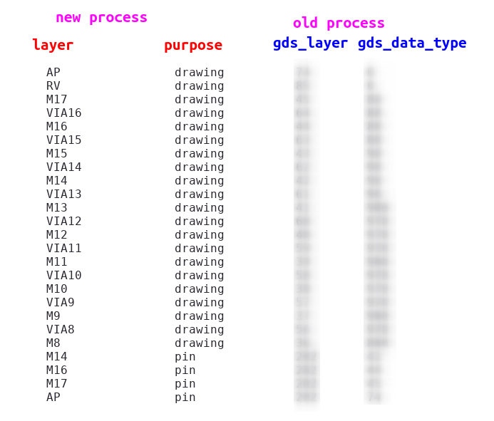
layout porting
streamout in old process -> streamin in new process with layermap,
format in below
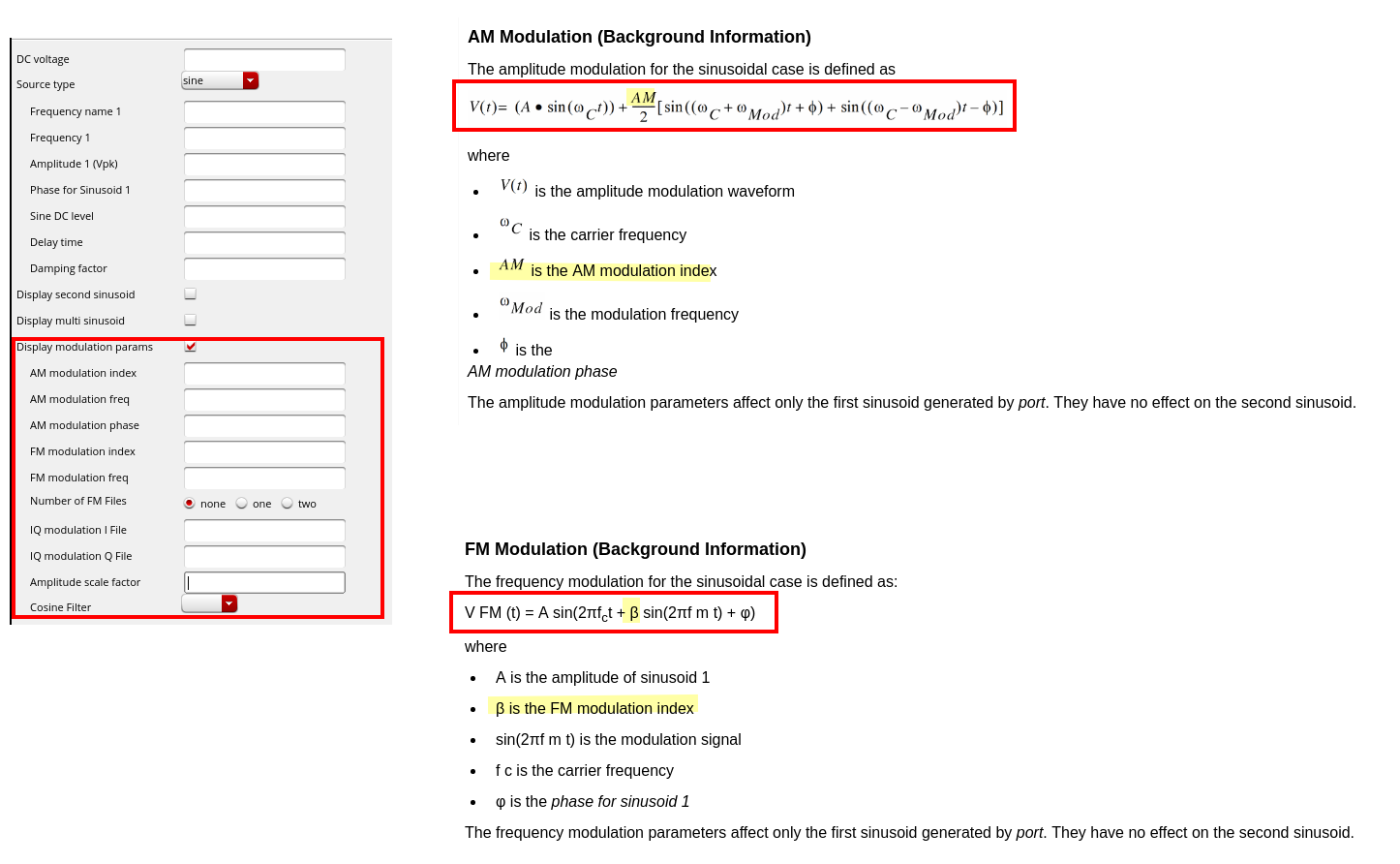
Modulation index in Virtuoso
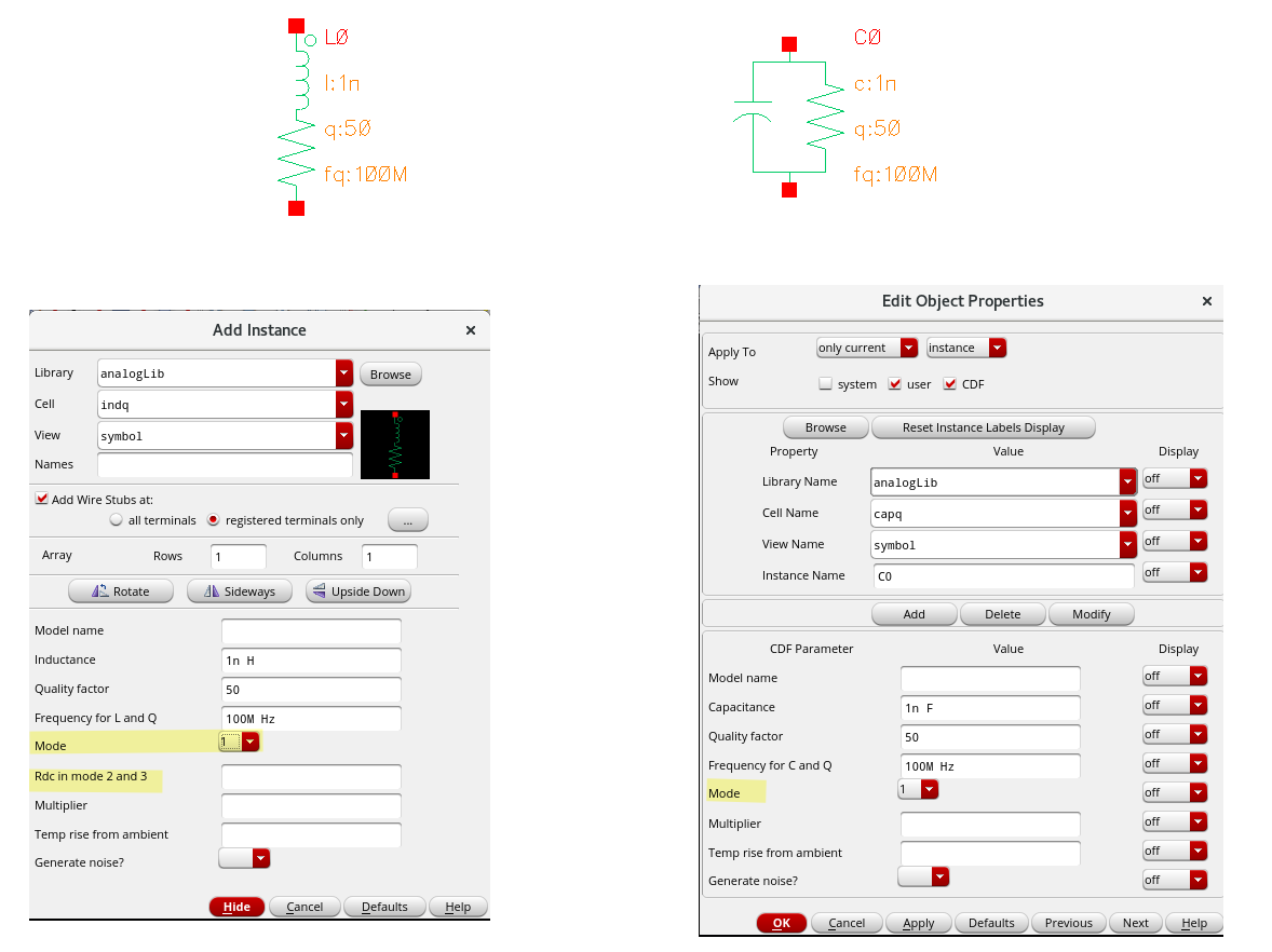
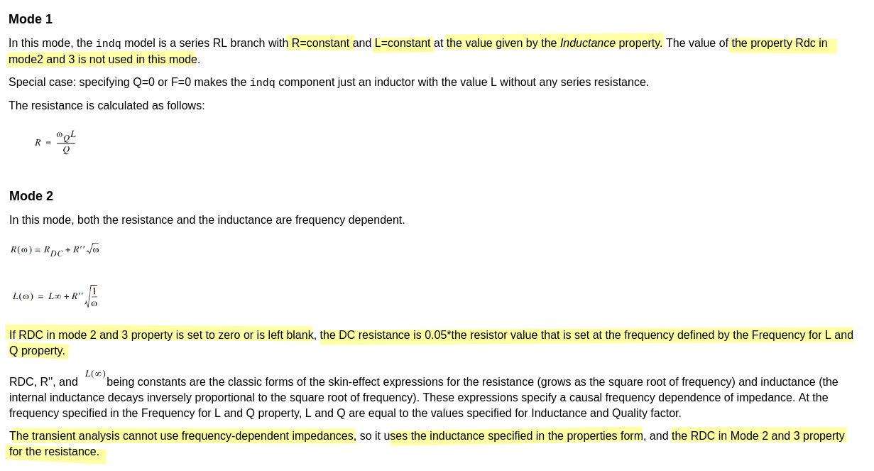
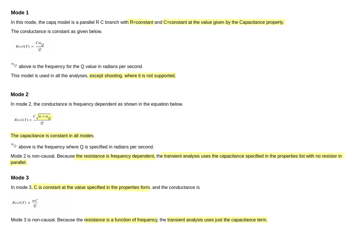
indq, capq
The inductor with Q works in all the analyses except
for shooting.
The capacitor with Q
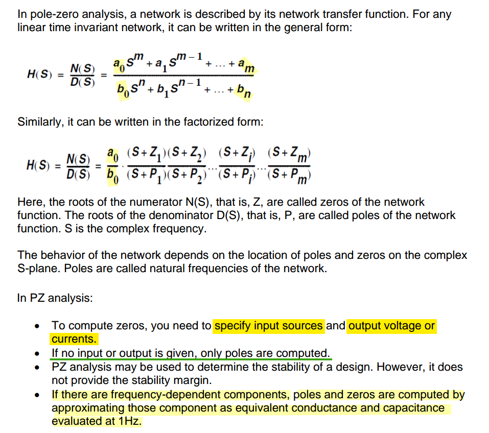
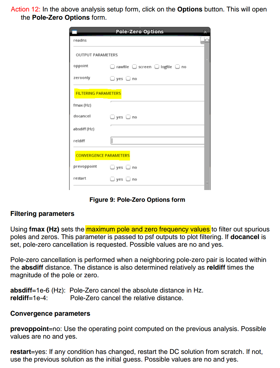
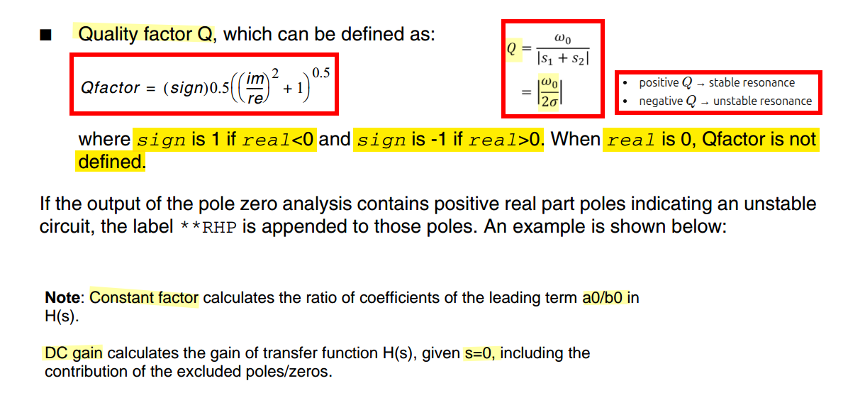
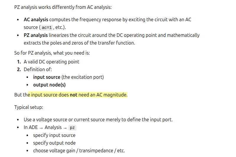
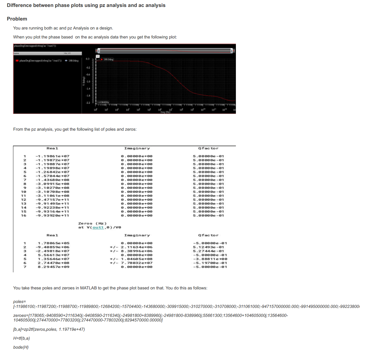
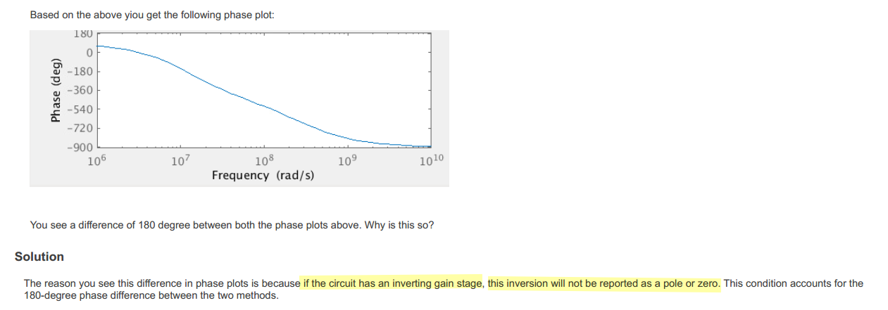
Pole Zero (PZ) Analysis
Pole Zero (PZ) Analysis with Spectre/SpectreX Rapid Adoption Kit
(RAK)
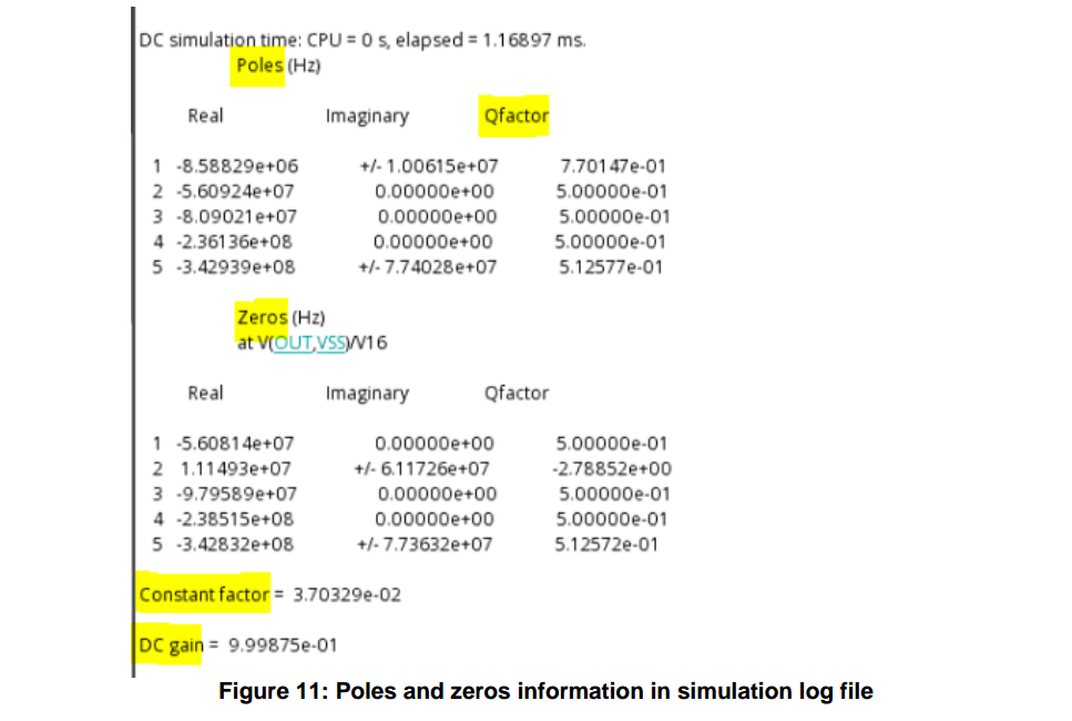
Note: poles/zeros in simulation log are in Hz instead of
rad/s
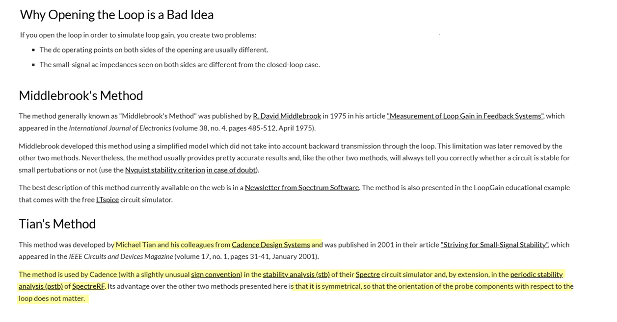
M. Tian, V. Visvanathan, J. Hantgan and K. Kundert, "Striving for
small-signal stability," in IEEE Circuits and Devices Magazine, vol. 17,
no. 1, pp. 31-41, Jan. 2001 [https://kenkundert.com/docs/cd2001-01.pdf]
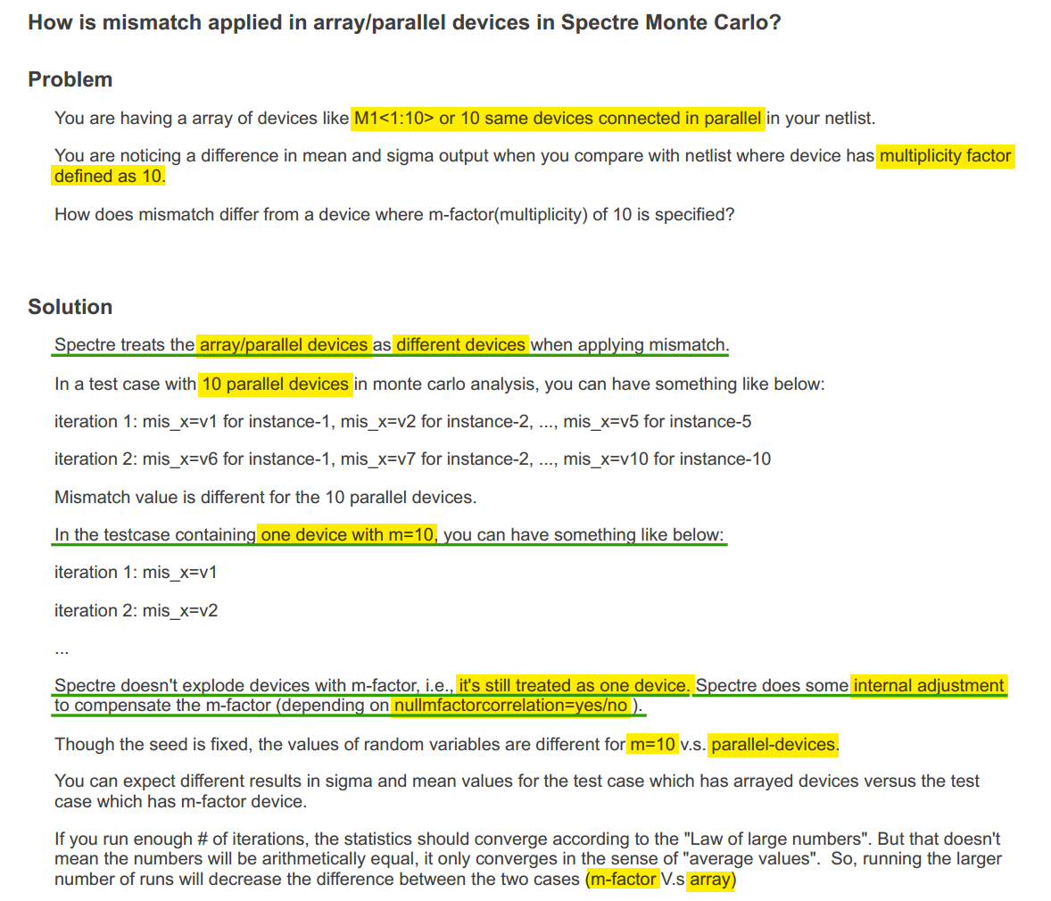
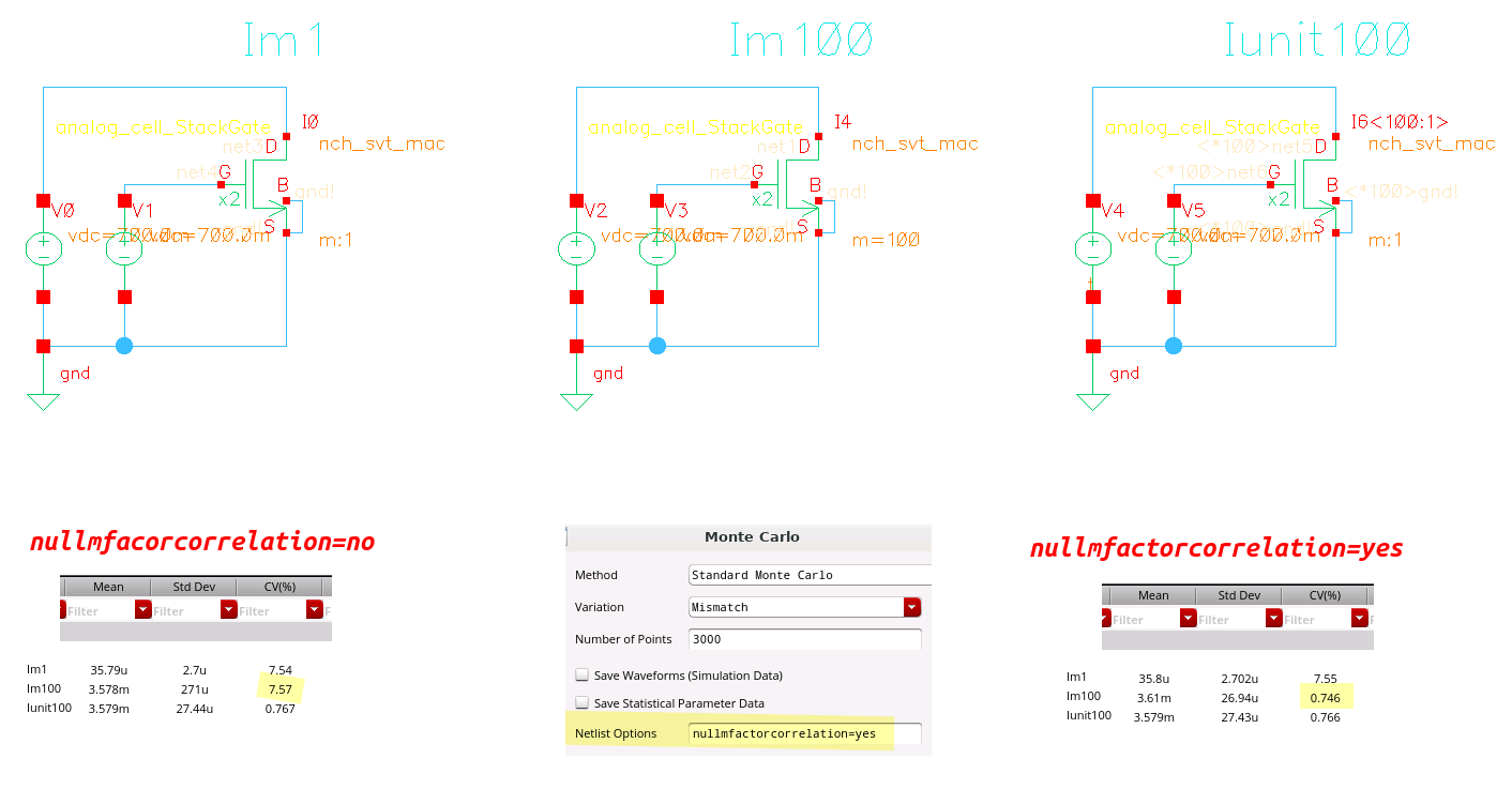
cadence support, How is mismatch applied in array/parallel
devices in Spectre Monte Carlo?
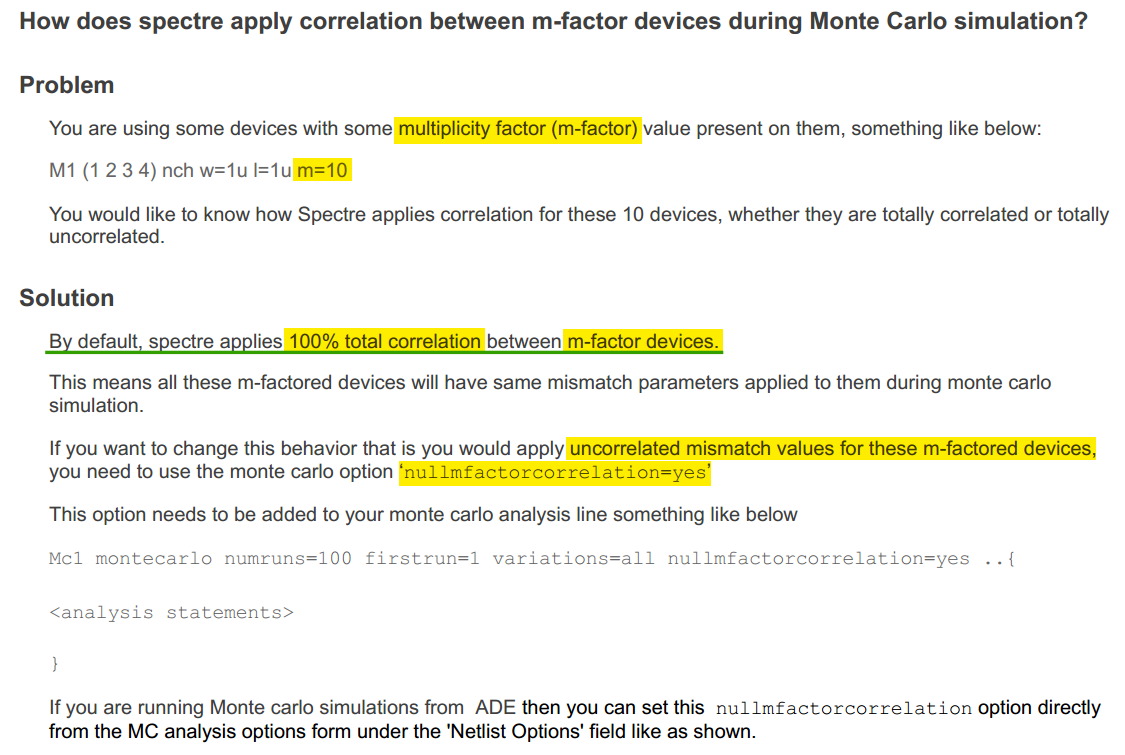
—, How does spectre apply correlation between m-factor devices
during Monte Carlo simulation?
nullmfactorcorrelation=no/yes
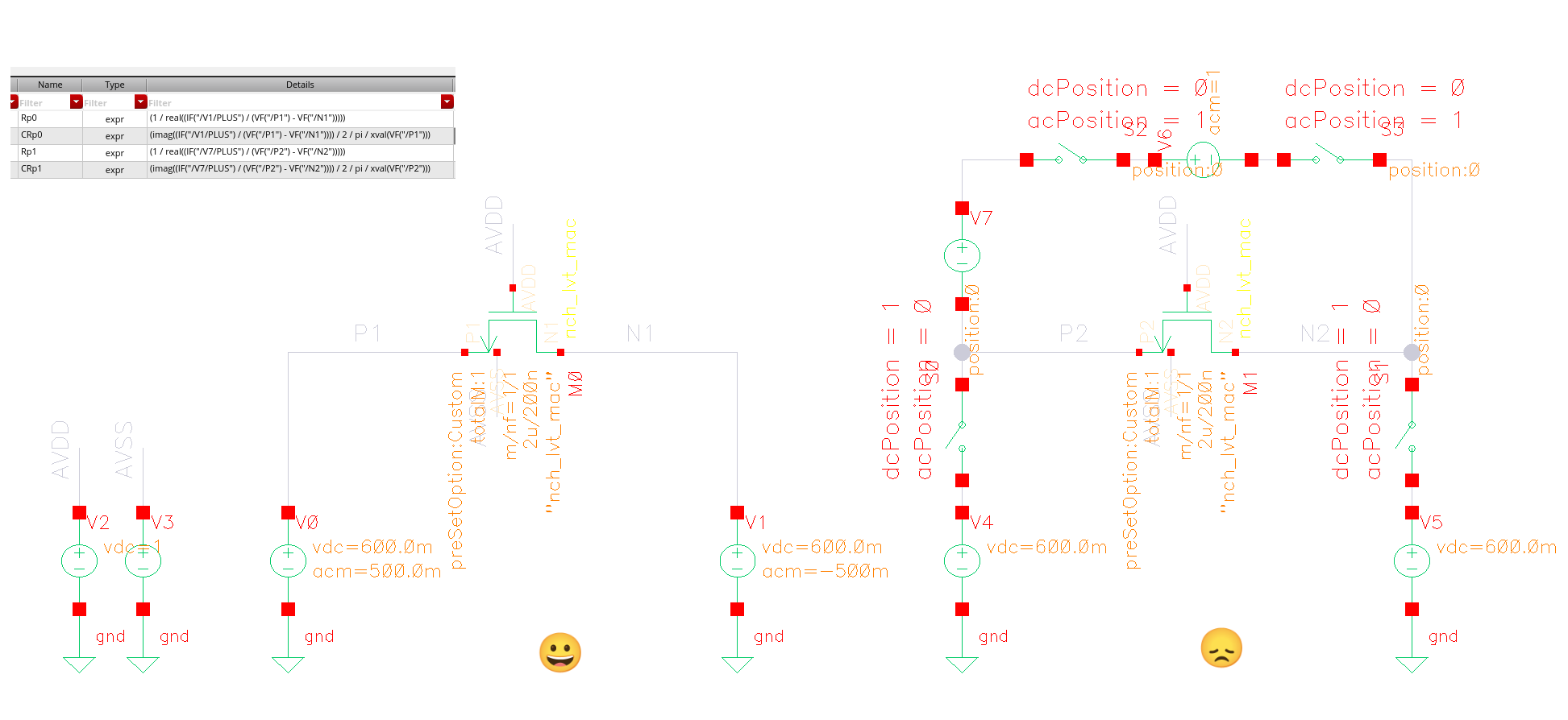
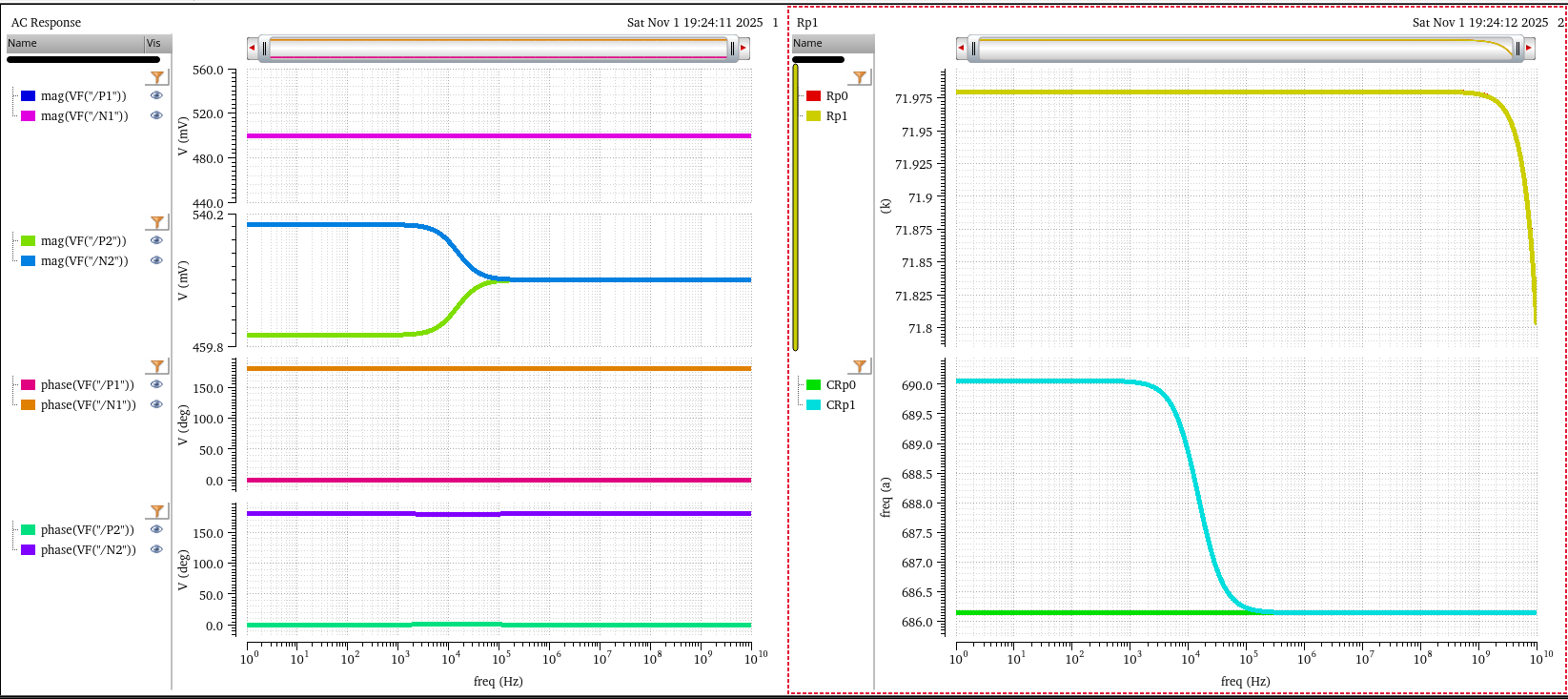
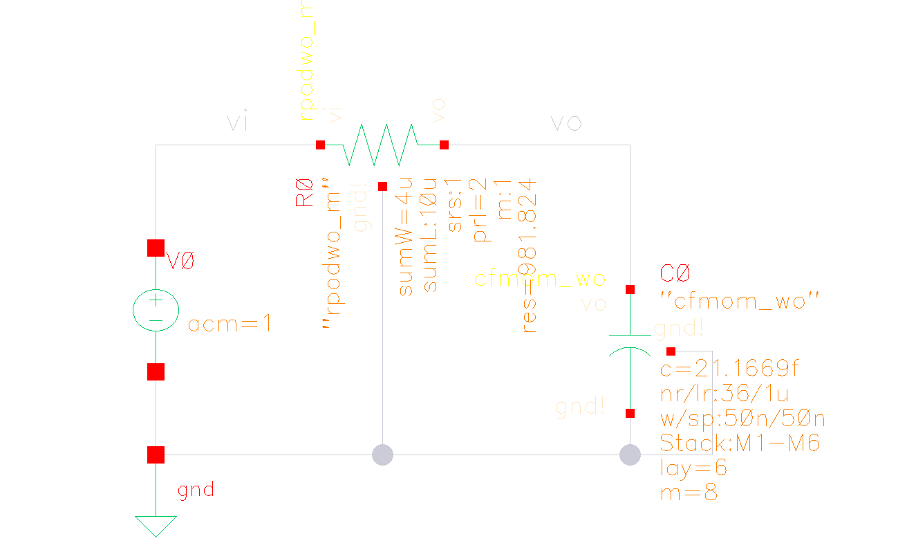
differential R/C simulation
The left testbench is better choice for differential R/C extraction.
because the right testbench may have uncontrolled AC common
stimulus, which is undesired
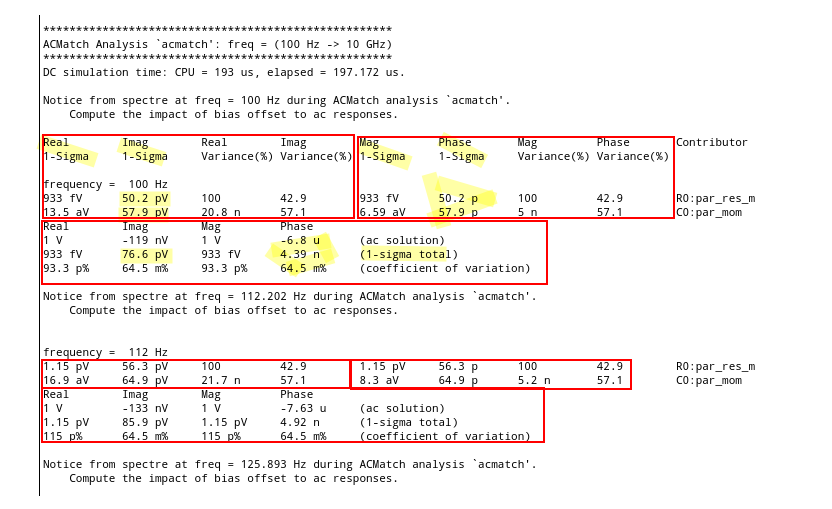
ACMatch analysis linearizes the circuit about the DC operating point
and computes the variations of AC responses
due to statistical parameters defined in statistics blocks.
Only mismatch parameters are considered. The analysis skips the
process parameters.
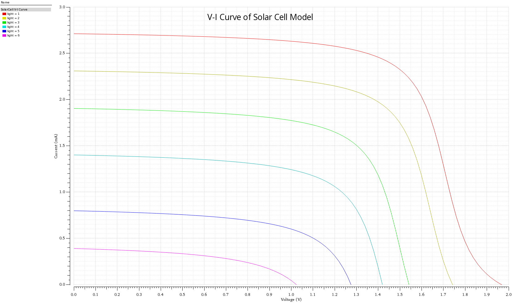
//Curve parameters real gm; real A; real factor; real Vop; real vcp;
integer light_i; integer en; analog begin
@(initial_step) begin en = 0; A = 1; Vop = 1; factor = 10; end //Enable digitalization @(cross(V(EN)-vthreshold,1)) begin if(V(EN)>=vthreshold) en = 1; else en = 0; end case(light): 0: begin A = 0; Vop = 0; end 1: begin A = -1.2; Vop = 1.71; end 2: begin A = -0.8; Vop = 1.64; end 3: begin A = -0.4; Vop = 1.50; end 4: begin A = 0.1; Vop = 1.43; end 5: begin A = 0.7; Vop = 1.36; end 6: begin A = 1.1; Vop = 1.22; end default: begin A = -1.2; Vop = 1.71; end endcase
//gm = A + atan(factor*(Vop-V(Vsolar))); //Transconductance
alias bk hiSetBindKey when ( isCallable('schGetEnv') bk("Schematics" "Ctrl<Key>x" "schHiCreateInst(\"basic\" \"nonConn\" \"symbol\")") bk("Schematics" "Ctrl<Key>v" "schHiCreateInst(\"analogLib\" \"vdc\" \"symbol\")") bk("Schematics" "Ctrl<Key>g" "schHiCreateInst(\"analogLib\" \"gnd\" \"symbol\")") bk("Schematics" "Shift<Key>9" "geDeleteNetProbe()") bk("Schematics" "<Key>0" "geDeleteAllProbe(getCurrentWindow()t)") ) unalias bk
leBindKeys.il
layout
1 2 3 4 5 6 7 8 9 10 11 12 13 14 15 16
alias bk hiSetBindKey when ( isCallable('leGetEnv) bk("Layout" "<Key>1" "leSetEntryLayer(\"M0PO\") leSetAllLayerVisible(nil) leSetEntryLayer(\"M0OD\") leSetEntryLayer(\"VIA0\") leSetEntryLayer(list(\"M1\" \"pin\")) leSetEntryLayer(\"M1\") hiRedraw()" ) ; M1-VIA1-M2 bk("Layout" "<Key>2" "leSetEntryLayer(\"M1\") leSetAllLayerVisible(nil) leSetEntryLayer(\"VIA1\") leSetEntryLayer(list(\"M2\" \"pin\")) leSetEntryLayer(\"M2\") hiRedraw()" ) ; M2-VIA2-M3 bk("Layout" "<Key>3" "leSetEntryLayer(\"M2\") leSetAllLayerVisible(nil) leSetEntryLayer(\"VIA2\") leSetEntryLayer(list(\"M3\" \"pin\")) leSetEntryLayer(\"M3\") hiRedraw()" ) ; M3-VIA3-M4 bk("Layout" "<Key>4" "leSetEntryLayer(\"M3\") leSetAllLayerVisible(nil) leSetEntryLayer(\"VIA3\") leSetEntryLayer(list(\"M4\" \"pin\")) leSetEntryLayer(\"M4\") hiRedraw()" ) ; M4-VIA4-M5 ; select M4 layer, turn off other layer visibilty, select VIA4 M5_pin M5 and turn on them bk("Layout" "<Key>5" "leSetEntryLayer(\"M4\") leSetAllLayerVisible(nil) leSetEntryLayer(\"VIA4\") leSetEntryLayer(list(\"M5\" \"pin\")) leSetEntryLayer(\"M5\") hiRedraw()" ) ; all visiable bk("Layout" "<Key>0" "leSetAllLayerVisible(t) hiRedraw()" ) ) unalias bk
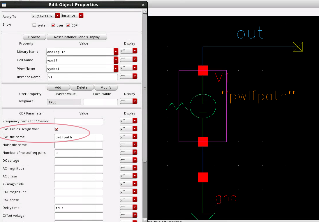
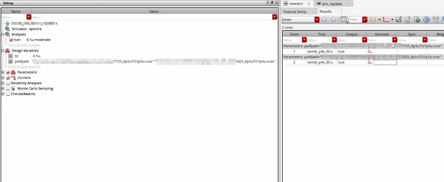
Design Variable in vpwlf
PWL File as Design Var? parameter in vpwlf cell
is convenient for sweep simulation or corner simulation, wherein there
are multiple pwl files .
The file path should be surrounded with
double-quotes to be protected from evaluation.
save option
Using Spectre Save Effectively RAK
none:
Does not save any data (currently does save one node chosen at
random)
selected:
Saves only signals specified with save statements. The default
setting.
lvlpub:
Saves all signals that are normally useful up to nestlvl deep in the subcircuit hierarchy. This option is equivalent to allpub for subcircuits.
lvl:
Saves all signals up to nestlvl deep in the subcircuit hierarchy.
This option is relevant for subcircuits.
allpub:
Saves only signals that are normally useful.
all:
Saves all signals.
Signals that are "normally useful" include the shared node voltages
and currents through voltage sources and iprobes, and exclude the
internal nodes on devices (the internal collector, base, emitter on a
BJT, the internal drain, source on a FET, and so on). It also excludes
currents through inductors, controlled sources, transmission lines,
transformers, etc.
If you use lvl or all instead of
lvlpub or allpub, you will also get
internal node voltages and currents through other components that happen
to compute current.
Thus, using *pub excludes internal nodes on devices
(the internal collector, base, emitter on a BJT, the internal drain and
source on a FET, etc). It also excludes the currents through inductors,
controlled sources, transmission lines, transformers, etc.
nestlvl
This variable is used to save groups of signals as results and when
signals are saved in subcircuits. The nestlvl parameter also specifies
how many levels deep into the subcircuit hierarchy you want to save
signals.
virtuoso "dlopen failed
to open 'libdl.so'"
1
$ sudo yum install glibc-devel
1 2 3 4 5 6 7 8 9 10 11 12 13 14 15
Last metadata expiration check: 0:01:02 ago on Sat 24 Sep 2022 12:13:54 AM CST. Dependencies resolved. ========================================================================================================================================= Package Architecture Version Repository Size ========================================================================================================================================= Installing: glibc-devel x86_64 2.28-189.5.el8_6 baseos 78 k Installing dependencies: glibc-headers x86_64 2.28-189.5.el8_6 baseos 482 k kernel-headers x86_64 4.18.0-372.26.1.el8_6 baseos 9.4 M libxcrypt-devel x86_64 4.1.1-6.el8 baseos 24 k
* DSPF files to use with Corner Definitions * This is an example file showing how to define different dspf files for different corners * using model files for individual components as the * building blocks. simulator lang=spectre library dspf_files_corners
section rcworst_25 dspf_include "DSPF_RC_WORSE25.spf" end section rcworst_25
section rcworst_125 dspf_include "DSPF_RC_WORSE125.spf" end section rcworst_125
endlibrary dspf_files_corners
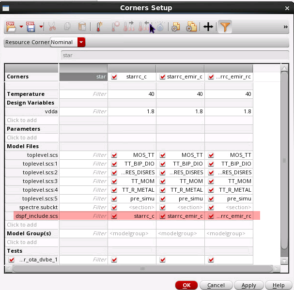
Add the file created above ‘myDSPF_File.scs’ in
‘Add/Edit Model Files’ of Corners setup form
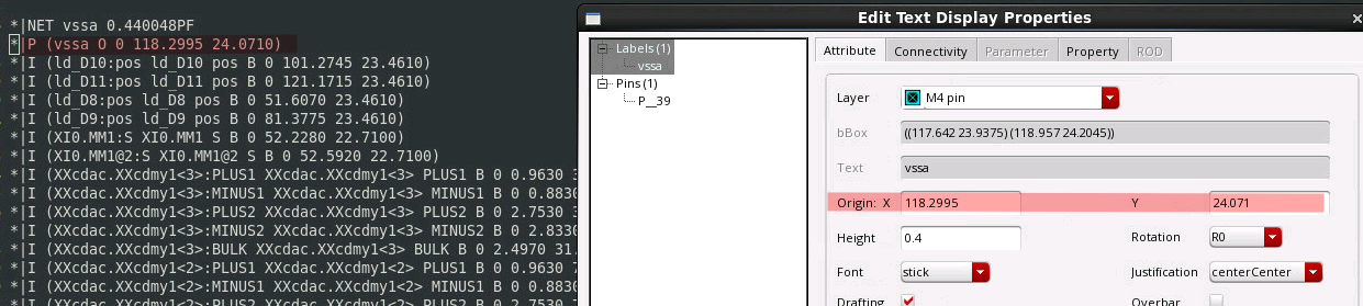
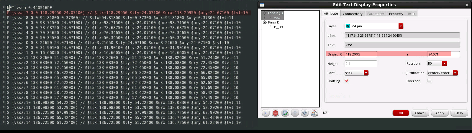
split pins in dspf_emir
dspf extract using starrc
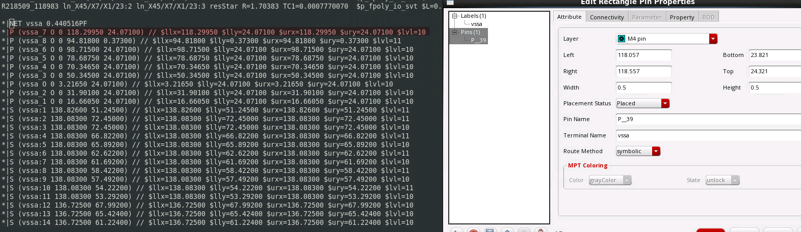
multiple label and rectangle in vssa net
general dspf
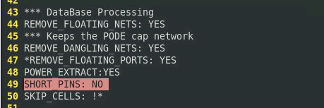
SHORT_PINS: YES
other pin are short together
dspf for emir analysis
It seems that dspf_emir don't contain the
rectangle pin information.
only label is necessary
setup
spectre result
netlist type
dspf option
emir analysis
dspf
/
disable
✓
dspf_emir
/
disable
✗
dspf_emir
shortPins="yes"
disable
✓
dspf_emir
shortPins="no"
disable
✗
dspf_emir
/
enable
✓
dspf_emir
shortPins="yes"
enable
✓
dspf_emir
shortPins=”no”
enable
✓
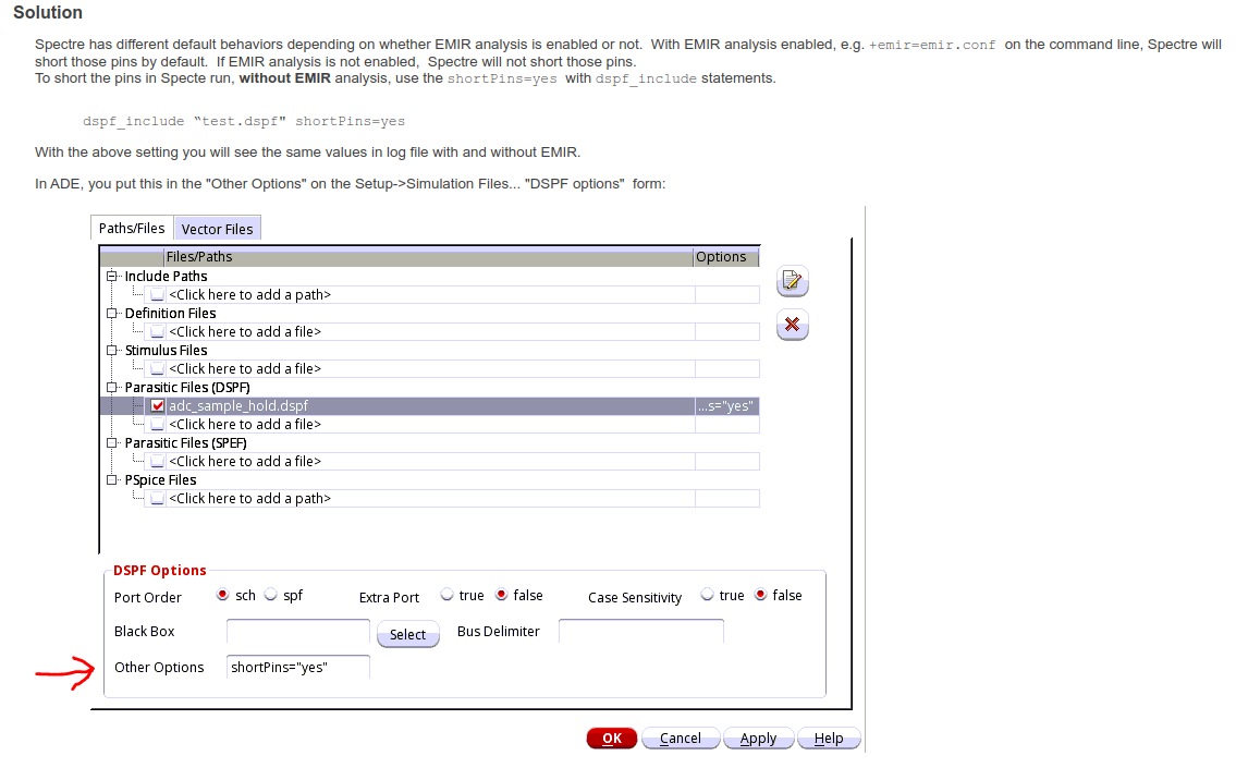
shortPins="yes" is preferred default option for
dspf_emir, which has split pins
DSPF Syntax
::=*|P ?
describes pins in the net. Multiple pin descriptions can be listed in
one line.
::=( {}?)
represents the name of the pin. represents the type
of the pin. It can be any of the following: I (Input), O (Output),
B (Bidirectional), X (don’t care), S (Switch), and J (Jumper).
represents the capacitance value associated with the pin.
is optional. It represents the location of the pin. Multiple pin
locations are allowed
split pins
1 2 3 4 5
*|P (avss_1 O 0 207.7555 59.9170) *|P (avss_10 O 0 181.1610 151.1130) *|P (avss_11 O 0 186.6330 151.1130) *|P (avss_12 O 0 192.1050 151.1130) *|P (avss_13 O 0 197.5770 151.1130)
reference
Article (20467964) Title: Difference in result on running Spectre APS
with EMIR and without EMIR analysis
StarRC User Guide and Command Reference Version O-2018.06, June
2018
DSPF Options
Case Sensitivity
netlist format
default option
Spectre netlist
case sensitive
dspf format
case insensitive
For a dspf format, it will be treated as a spice
netlist format, which is by default case insensitive
Pay attention to VerilogIn block, which may contain upper
case / lower case net name, e.g NET1 and net1.
The extracted DSPF using extraction tool also contain NET1 and net1,
which shall not be shorted together.
Port Order
If you use .dspf_include, the following rules apply:
The subcircuit description is taken from the DSPF file even if the
same subcircuit description is available in the schematic netlist.
Depending on the port_order option, the port order of
the subcircuit definition is taken from the pre-layout schematic netlist
or from the DSPF file subcircuit definition, as shown below.
port_order=sch – (Default). The port order is taken
from schematic subcircuit definition. The same port number and names are
required. If the schematic subcircuit definition is not available, a
warning is issued in the log file, and DSPF port order is used.
port_order=spf – The port order is taken from the DSPF
subcircuit definition.
SPICE_SUBCKT_FILE of StarRC
The StarRC tool reads the files specified by the
SPICE_SUBCKT_FILE command to obtain port ordering
information. The files control the port ordering of the top
cell as well. The port order and the port list members read from the
.subckt for a skip cell are preserved in the output
netlist.
The file usually is the cdl netlist of extracted cell, this
way, port order is not problem
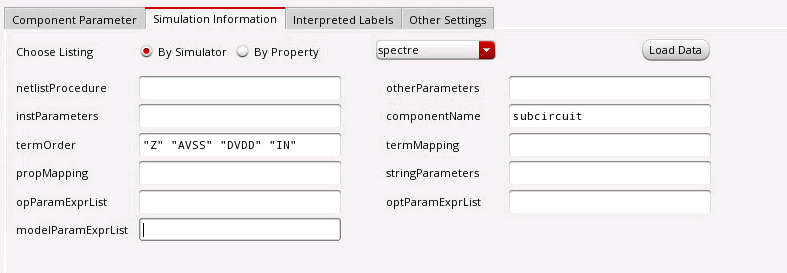
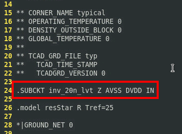
CDF termOrder
DSPF same order
DSPF
input.scs
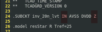
different order
manual change DSPF's pin order shown as below
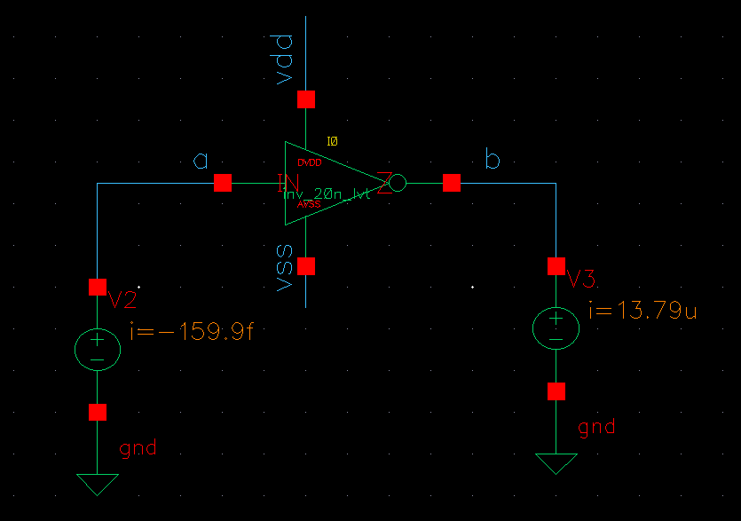
port_order=sch
dspf port is mapping to schematic by name, and the
simulation result is right
port_order=spf
dspf pin order is retained, and no mapping between
spectre netlist and dspf.
The simulation result is wrong
bus_delim="_ <>"
The way this works is that the first part of bus_delim is
the "schematic" delimiter (i.e. what's in the spectre netlist), and the
other part is the DSPF delimiter
reference
Article (20502176) Title: How does Spectre understand case-sensitive
net names when using various post-layout netlists such as dspf,
av_extracted view, or smart view?
Spectre Tech Tips: Using DSPF Post-Layout Netlists in Spectre Circuit
Simulator - Analog/Custom Design - Cadence Blogs - Cadence Community https://shar.es/afO6e1
StarRC™ User Guide and Command Reference Version O-2018.06, June
2018
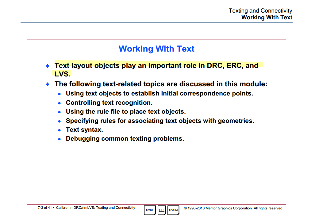
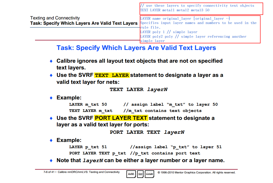
Virtual Connectivity
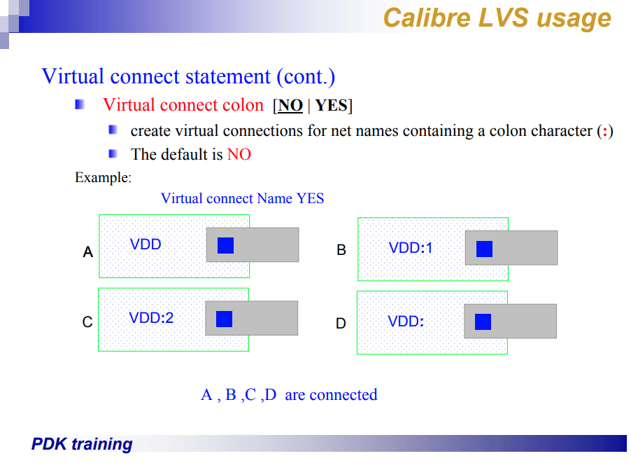
Normally, if the layout connectivity extractor finds disjoint,
unconnected geometries with the same net name text attached, the
extractor will view this as an open circuit.
Virtual connection results in the extraction of a single net from
two or more disjoint physical nets when the physical net segments share
the same name.
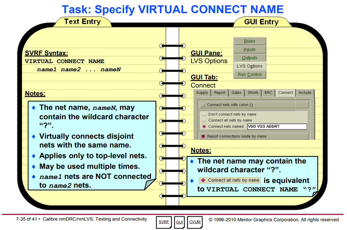
Virtual connectivity is triggered by the rule file VIRTUAL
CONNECT COLON and VIRTUAL CONNECT NAME
specification statements.
Virtual connectivity can also be specified through the Calibre
Interactive GUI.
Virtual connectivity is of primary interest in
LVS applications
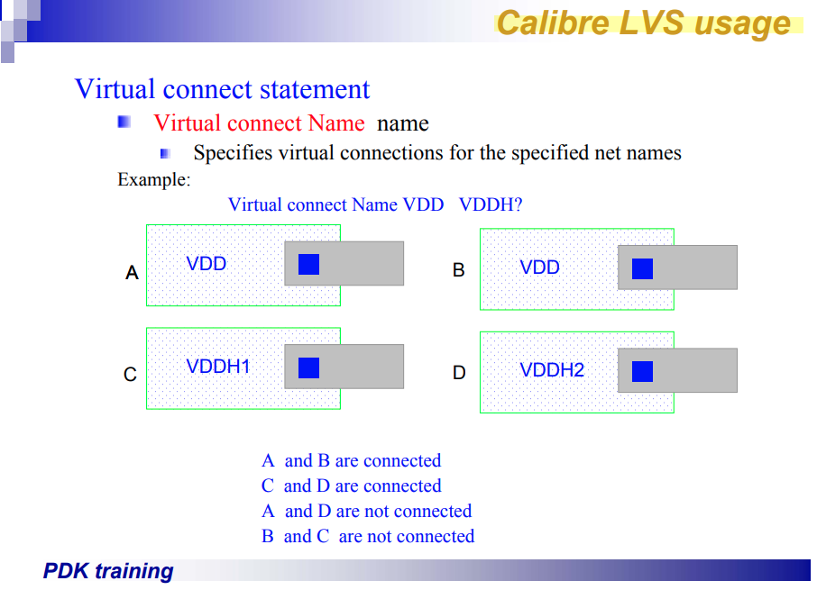
connect all nets by name:
VIRTUAL CONNECT NAME "?"
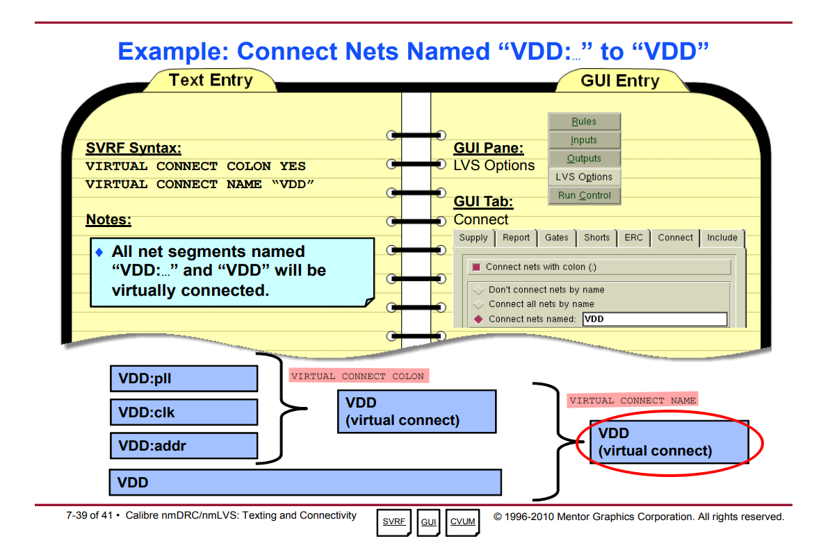
VIRTUAL CONNECT COLON
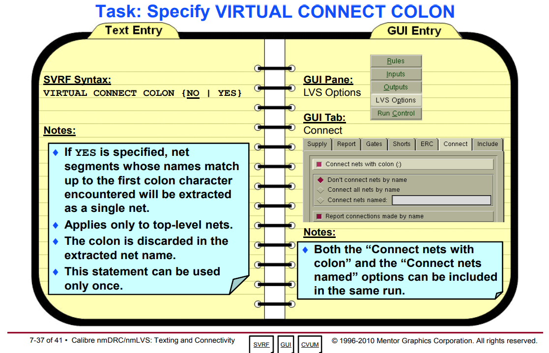
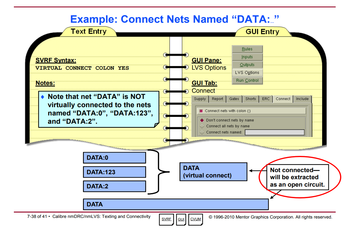
Virtual Connect Colon is used to virtually connect
nets that share a common prefix before a colon, like
VDD:1, VDD:2, and so forth.
If you specify YES, then the connectivity extractor first
strips off all characters from the first colon to the end of
the label names.
Next, the extractor forms a virtual connection between any two labels
that have the same name and that originally contained a
colon.
Colons can appear anywhere in the name with the exception that a
colon at the beginning of a name is treated as a regular character (that
is, it has no special effect).
up to the first colon character encountered
The colon is discarded in the extracted net
name
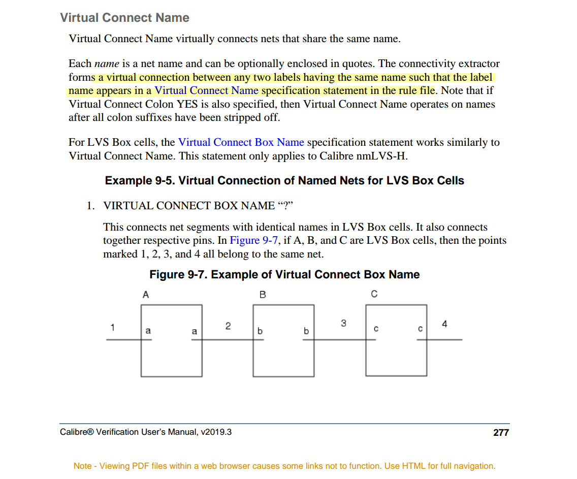
VIRTUAL CONNECT NAME
Virtual Connect Name virtually connects nets that
share the same name
Each name is a net name and can be optionally enclosed in quotes.
The connectivity extractor forms a virtual connection between
any two labels having the same name such that
the label name appears in a Virtual Connect Name
specification statement in the rule file.
VIRTUAL CONNECT NAME ? == Connect all nets by name
Note that if Virtual Connect Colon YES is also
specified, then Virtual Connect Name operates on names
after all colon suffixes have been stripped off.
Calibre Interactive stores a list of your most recently opened
runsets in your home directory as .cgidrcdb or
.cgilvsdb for Calibre Interactive DRC or LVS,
respectively.
When invoked, the Calibre DRC and LVS windows automatically load the
runset used when the last session was closed.
Runsets are ASCII files that set up Calibre Interactive for a Calibre
run. They contain only information that differs from the default
configuration of Calibre Interactive. There is a one-to-one
correspondence between entry lines in the runset file and fields and
button items in the Calibre Interactive user interface. Here is as
example of a DRC runset:
The runset filename opened at startup (if no runset is specified on
the command line) can also be specified by setting the
MGC_CALIBRE_DRC_RUNSET_FILE environment variable for DRC,
and the MGC_CALIBRE_LVS_RUNSET_FILE environment variable
for LVS. If these environment variables are set, they take precedence
over all other runset opening behavior options.
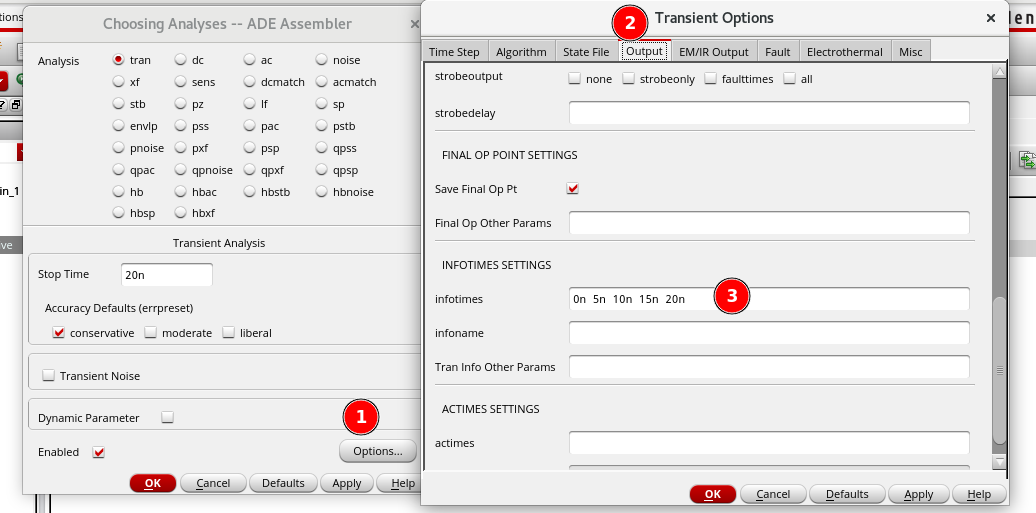
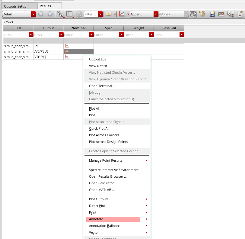
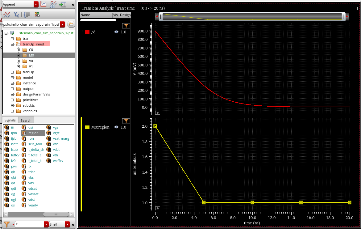
On the transient options form, there's a field called "infotimes" -
specify the times at which you want it to output the dc operating point
data. You can then annotate the "transient operating points" from any of
these times after the simulation, or access them via the results
browser.
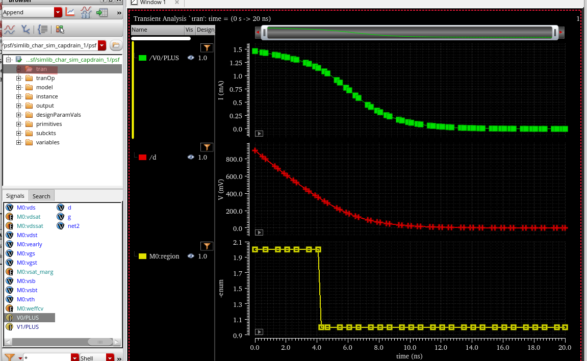
Or you could get the operating point data to be continuously saved
during the transient for selected devices - if so, create a file called
(say) "save.scs" (make sure it has a ".scs" suffix), and put: save
M1:oppoint or save M*:oppoint sigtype=dev in this file, and then
reference the file via Setup->Model Libraries or as a "definition
file" on Setup->Simulation Files. With this approach you can then
find the operating point data for the selected devices in the results
browser and plot it versus time (be cautious of saving too much though
because this can generate a lot of data if you're not careful)
<divider> represents the hierarchical pathname
divider. The default hierarchical character is forward slash
(/).
*|DELIMITER <delimiter>
<delimiter> represents the delimiter character
used to concatenate an instance name and pin name to form an instance
pin name.
It is also represents the delimiter character used to concatenate a
net name and subnode number to form a subnode name. The default
character is colon (:)
*|BUSBIT <left_busbit_char><right_busbit_char>
<left_busbit_char> and
<right_busbit_char> are used at the end of an
identifier of an array to select a single object of the array.
Objects which may be indexed include nets, primary pins, and
instance pins
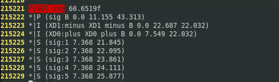
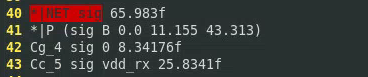
*|NET <netName> <netCap>
<netName> represents the name of a net. It can be
a user-provided net name, the name of the driving pin, or the name of
the driving instance pin.
<netCap> represents the total
capacitance value in farads associated with the net. This may be
comprised of capacitances to ground and capacitances to nearby
wires.
*|P <pinName> <pinType> <pinCap> {<coord>}
<pinName> represents the name of the pin.
<pinType> represents the type of the pin. It can
be any of the following: I (Input), O (Output), B (Bidirectional), X
(don’t care), S (Switch), and J (Jumper).
<pinCap> represents the capacitance value
associated with the pin.
<coord> is optional. It represents the location
of the pin. Multiple pin locations are allowed.
*|S <subNodeName> {<coord>}
subnodes in the net
<subNodeName> represents the name of the subnode.
A subnode name is obtained by concatenating the net name and a subnode
number using the delimiter specified in the DELIMITER statement. The
default delimiter is colon (:).
<instPinName> represents the name of the instance
pin. An instance pin name is obtained by concatenating the
<instName> and the <pinName> with
a delimiting character which is specified by the DELIMITER
statement
<instName> represents the name of the
instance
*|DeviceFingerDelim "@"
MOS finger delimiter
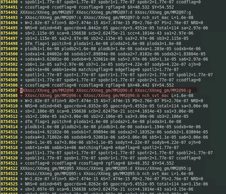
For example, M8's finger is 4, then split into 4 Devices
in DSPF
MM8, MM8@2, MM8@3,
MM8@4
its drain terminal will be
MM8:d, MM8@2:d, MM8@3:d,
MM8@4:d
DSPF Syntax
DSPF has two sections:
a net section
The net section consists of a series of net description blocks. Each
net description block corresponds to a net in the physical design. A net
description block begins with a net statement followed by pins, instance
pins, subnodes, and parasitic resistor/capacitor
(R/C) components that characterize the
electrical behavior of the net.
an instance section
The instance section consists of a series of SPICE instance
statements. SPICE instance statements begin with an
X.
Each file consists of hierarchical cells and interconnects only.
The DSPF format is as generic and as much like SPICE as possible.
While native SPICE statements describe the R/C sections, some non-native
SPICE statements complete the net descriptions. These non-native SPICE
statements start with the notation "*|" to differentiate them from
native SPICE statements. For native SPICE statements, a continuation
line begins with the conventional "+" sign in the first column.
The native SPICE statements used by the DSPF format are listed
below:
.SUBCKT represents a subcircuit statement.
.ENDS represents the end of a subcircuit
statement.
R represents a resistor element.
C represents a capacitor element.
E represents a voltage-controlled voltage sources
element.
X represents an instance of a cell;
* represents a comment line unless it is
*| or *+.
.END is an optional statement that represents the end
of a simulation session
spectre netlist
hier_delimiter="."
Used to set hierarchical delimiter. Length of
hier_delimiter should not be longer than 1, except the
leader escape character
This option maps the bus delimiter between schematic netlist and
parasitic file (i.e. DSPF, SPEF, or DPF). The option defines the bus
delimiter in the schematic netlist, and optionally the bus delimiter in
the parasitic file. By default, the bus delimiter of the parasitic file
is taken from the parasitic file header (i.e. |BUSBIT [],
|BUS_BIT [], or *|BUS_DELIMITER []). If the bus delimiter is not
defined in the parasitic file header, you need to specify it by using
the spfbusdelim option in schematic netlist.
Exampel
spfbusdelim=<> - A<1> in the schematic netlist is mapped
to A_1 in the DSPF file, if the bus delimiter header in the DSPF file is
"_".
spfbusdelim=@ [] - A@1 in the schematic netlist is mapped to to A[1]
in the DSPF file (the bus delimiter in DSPF header will be
ignored).
How to Save Net voltage in
DSPF
!!! follow the name of net section in DSPF - prepend to top-level
devices in the schematic with X
Assume node n1...n4 are named as below in DSPF file (prefix
X)
n1
XXosc/zip:1
n2
XXosc/zip:2
n3
XXosc/zip:3
n4
XXosc/zip:4
To save these nodes, you can add follow code in Definition
Files
saveopt.scs
1 2 3 4
save Xwrapper.Xvco.XXosc\/zip\:1 save Xwrapper.Xvco.XXosc\/zip\:2 save Xwrapper.Xvco.XXosc\/zip\:3 save Xwrapper.Xvco.XXosc\/zip\:4
Escape character \ is used for hierarchical pathname
divider / and subnode :
By the way, . is hierarchical delimiter of
Spectre
Calibre always prepend one X to instance name of
schematic in generated DSPF file
The DSPF design is flatten, the DIVIDER character
indicate the hierarchy
1
save Xwrapper.Xvco.XXosc\/zip
The above save voltage, however I'm NOT sure which node it save.
To avoid this unsure problem, the MOS terminal may be better choice
to save.
But keep in mind
OD resistance is lumped in the FEOL model
M0OD and above layer resistances are extracted by RC tool
How to Save Current in DSPF
!!! follow the name of instance section of DSPF - prepend to
top-level devices in the schematic with XX
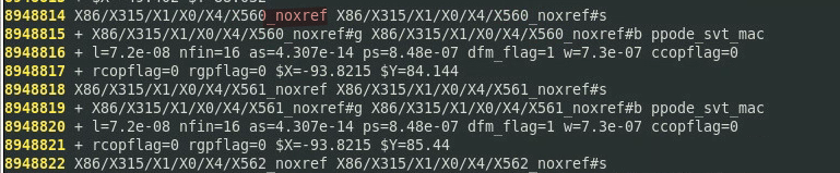
MOS in schematic: Xsupply.M4
MOS related information in DSPF (prefix XX in instance
section):
1 2 3 4 5 6 7 8 9
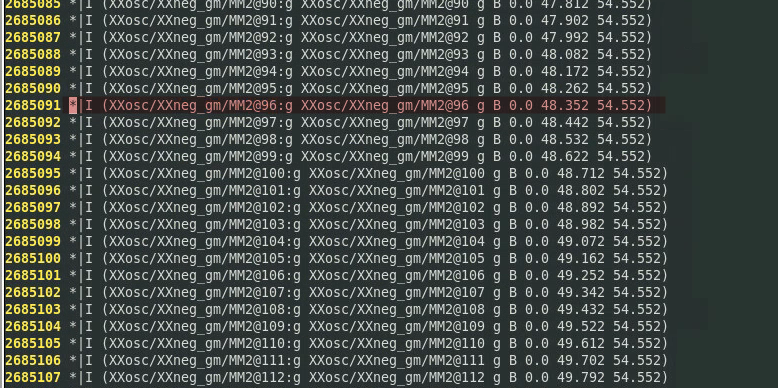
... // net section *|I XXsupply/MM4:d XXsupply/MM4 d B 0.0
<instName> in
*|I <instPinName> <instName> <pinName> <pinType><pinCap> {<coord>?}
which has prefix X corresponding to schematic is
NOT the instance name in DSPF. The instance name is in
instance section and has prefix XX
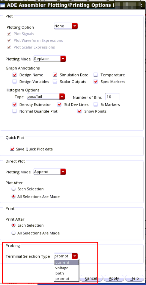
!!! Only work for MOS terminal current. Fail to apply to block
pin
Thinking about voltage
and current save
MOS device always prepend with M
To save net voltage, take account of the prefix
X of top-level device
To save MOS terminal, take account of the prefix
XX of top-level device
Post-layout netlists are created by layout extraction tools - Mentor
Calibre
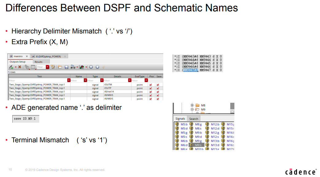
Differences
Between DSPF and Schematic Names
MOS Terminal Mismatch ( ‘s’ vs ‘1’)
Schematic: number '1' ,'2', '3','4'
DSPF: 'd', 'g', 's','b'
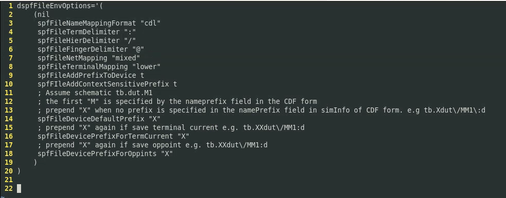
.simrc file
If DSPF files show such differences, you can set options in the
.simrc file to update the save statement in the
netlist so that the device names match with those in the DSPF
file
Additionally, dspf_include reads all the DSPF lines
starting with * (|NET, |I, *|P,*|S), while
include considers all related lines as comments.
Only verified to DSPF output of Mentor Calibre
1 2 3 4 5 6 7 8 9 10 11 12 13 14 15 16 17 18
; ensure that the netlist is recreated each time nlReNetlistAll=t
The net name is x1/x1:DRN. During the simulation, the following
warning is reported:
Warning from spectre during initial setup.
1 2
WARNING (SPECTRE-8282): `xpi1.x1/x1' is not a device or subcircuit instance name. WARNING (SPECTRE-8287): Ignoring invalid item `xpi1.x1/x1:DRN' in save statement.
How can I save this net for plotting and measurements?
Solution
The colon (:) in the save statement specifies terminal
current. So, the save statement used above is for terminal
current and, hence, the warning messages are reported.
1
save xpi1.x1\/x1:DRN
You need to modify the save statement as below:
1
save xpi1.x1\/x1\:DRN
Now, run the simulation and the issue will be resolved.
DSPF r vs rcc
rcc
c
only c dspf give the lumped
capacitance
EMIR via Voltus-Fi
general terminology
DC related
Imax in T*'s DRC document is the maximum allowed
DC current, which depends on Length and Width
only
Iavg is the average value of the current, which is
the effective DC current. Therefore, Iavg
rules are identical to Imax
rules \[
I_{\text{avg}}=\frac{\int_0^\tau I(t)dt}{\tau}
\] Similarly, Iabsavg rules are
identical to Imax rules, too \[
I_{\text{AbsAvg}}=\frac{\int_0^\tau |I(t)|dt}{\tau}
\]
rms
Irms is the root-mean-square of the current through
a metal line, which depends w(in um), the drawn
width of the metal line and \(\Delta
T\), the temperature rise due to Joule heating. \[
I_{\text{rms}}=\left[\frac{\int_0^\tau I(t)^2dt}{\tau} \right]^{1/2}
\]
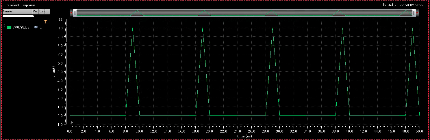
peak current
Ipeak in T*'s DRC document is the current at which a
metal line undergoes excessive Joule heating and can begin to melt.
Ipeak is corresponding to
EM Current Analysis: max in Voltus-Fi Analysis Setup \[
I_{\text{peak}}=\max(|I(t)|)
\] The limit for the peak current is \[
I_{\text{peak,limit}}=\frac{I_{\text{peak\_DC}}}{\sqrt{r
} }
\] where r is the duty ratio
The relationship between Ipeak and
Ipeak_DC is merged in DRC document so that there is
only Ipeak equation in document
\(I_{\text{peak,limit}}\) depends on
\(t_D\), r, width and length
\[
r=\frac{t_D}{\tau}
\]
where \(t_D\) is equivalent duration
\[
t_D =\frac{\int_0^\tau |I(t)|dt}{I_{\text{peak}}}
\] or \[
r=\frac{I_{\text{AbsAvg}}}{I_{\text{peak}}}
\]
where the drawn width is 1um, r is 0.1
\[
9.37*(1-0.004)/\sqrt0.1 = 29.512
\]
acpeak/pwc
It's same with max EM Current Analysis in
Voltus-Fi
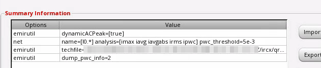
dynamicACPeak
This option affect how duty ratio r is computed in max
and acpeak/pwc EM current Analysis
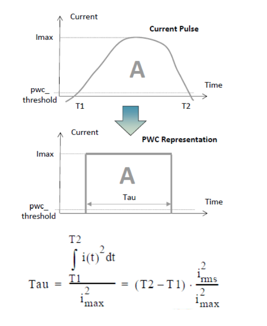
When the dynamicACPeak variable is set to
true or multiPeak\[
r=\frac{T_d}{T_{\text{total}}}
\]
where \(T_{\text{total}} = \text{EMIR time
window}\)
\(T_d\) = the time duration in
microsecond of the total "On Time" period based on IPWC
Pulse-Wise Constant EM current calculation (IPWC)
where Tau is \(T_d\) in above formula
!!! It seems that t*'s PDK don't support
dynamicACPeak=true
IR drop filter layers
EM techfile (qrcTechFile) may take diffusion contact
(n_odtap, p_odtap in DSPF file) into account during IR
drop analysis. And these segment often dominate IR drop, but we as IC
designer can NOT improve them. In general, the IR drop to M1 layer is
enough and feasible.
Regular
analysis statements in emir configuration
1 2
net name=[I0.vdd I0.vss] analysis=[vmax vavg] net name=[I0.*] analysis =[imax ivavg irms]
emirreport command
Creating reports for specific nets after simulation using
emirreport
Create a new config file as shown below:
1 2 3
** test.conf** net name=[I1.VDD I1.VSS] analysis=[iavg] net name=[I1.VBIAS] analysis=[imax]
Run emirreport on the command line using the
emirdatabase (emir*.bin) and test.conf
created above in
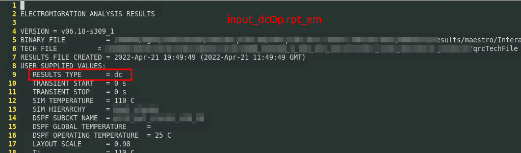
input.emir0_bin: The first EMIR Analysis which is DC or
Transient, which depends on Analyses order
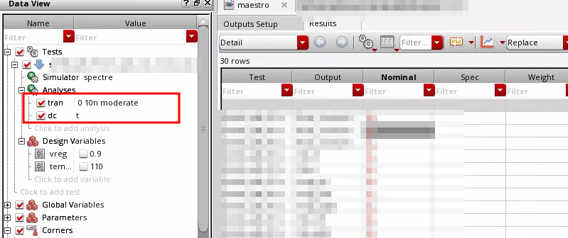
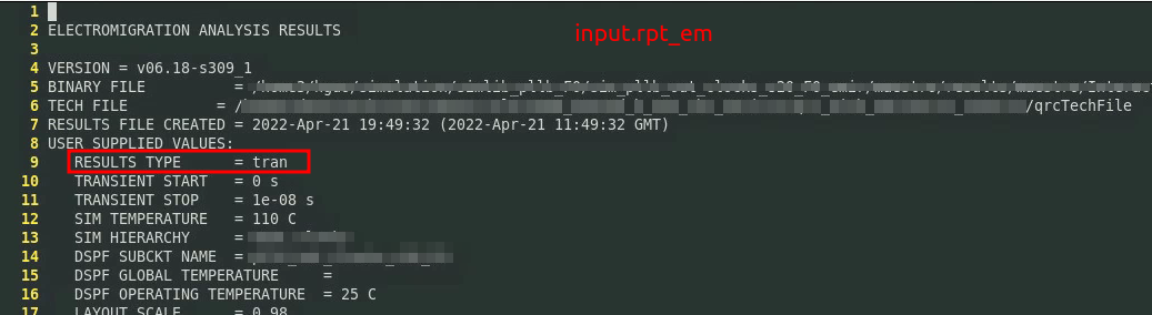
input_tran.emir0_bin: EMIR Analysis in Transient
simulation
input_dcOp.emir0_bin: EMIR Analysis in DC
simulation
For example
Two results are generated input.emir0_bin and
input_dcOp.emir0_bin and their reports respectly
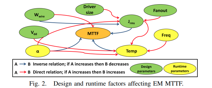
Fix Electromigration
Type
wider wire
downsize drivers
decrease fanout
RJ JMAX
✓
✓
JAVG
JABSAVG
JACPEAK
JACRMS
✓
✓
✓
Iavg
The average value of the current, which is the effective DC
current
Irms
Irms rule relates to the heat or Joule-heating of metal
lines
Ipeak
The main goal of the Ipeak limits is to ensure that no thermal
breakdown could occur on single overshoot events. If the signal may not
have a high current density but if it has a very large peak current
density, then, local melting will happen and cause failures
QA
Q. Why “length” column in EM results form doesn’t show extracted
length, it shows “NA”.
A. Voltus-Fi reports the “length” column only when length rules are
present in the emDataFile.
Seeing different port currents with and without emir simulations
for same dspf included in EMIR Direct method using dspf_include.
Split Pins (*|P) in DSPF are only shorted in the EMIR flow not in the
regular spectre flow. Islands patching is only performed in EMIR
only
Setting temperature for EM analysis
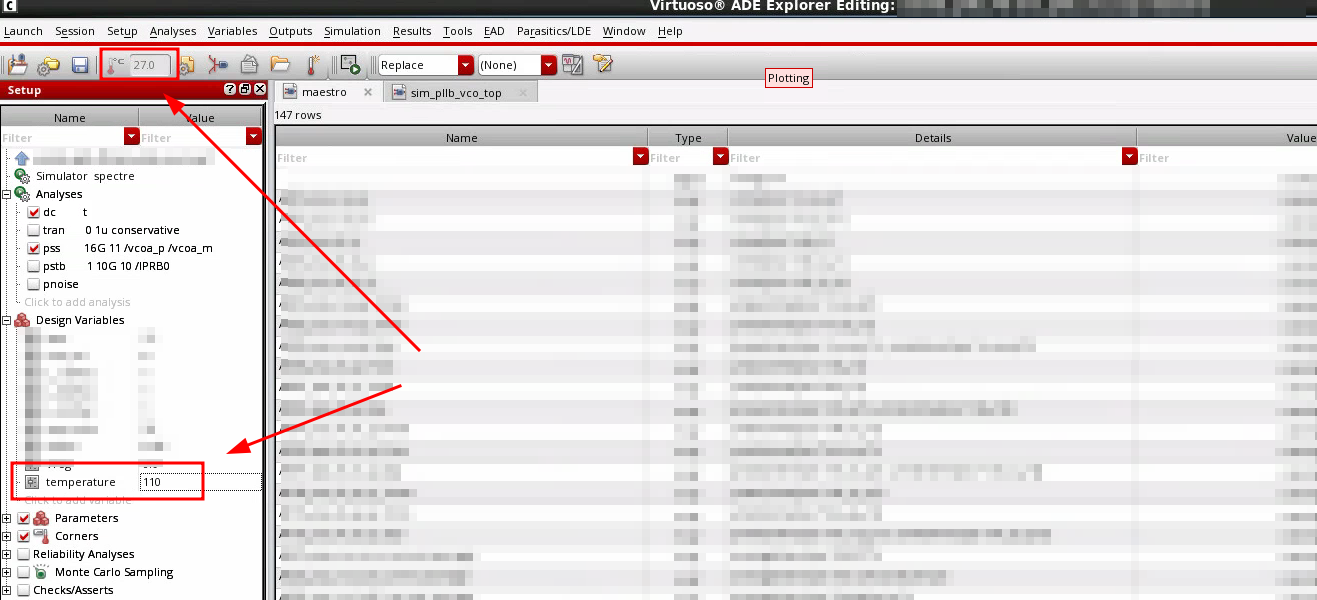
By Default, Voltus-FI and VPS pick up the current density limit for
temperature at which simulation has been performed.
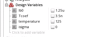
By the way, Design Variables - temperature will
override the temperature in Setup toolbar which is gray in ADE
Explorer
AC Peak EM analysis - Voltus-Fi
The available options within the EM current analysis section in the
EMIR Analysis Setup form are:
max / avg / avgabs / rms.
In order to enable the AC Peak based information when
loading the EM results, both max and avg should be
selected when setting up the EMIR Analysis Setup.
With this configuration, the AC Peak option becomes available and can
be used.
How to print average, rms, and peak current of device
tap in Spectre/Voltus FI EMIR analysis
The following option enables you to save the average, rms, and peak
tap currents in the emir0bin file and report it in the
input.rpt_tapi file.
1
solver report_tapi=true
Add this option in emir.conf to enable the reporting
of tap current after the Spectre EMIR simulation. The input.rpt_tapi
file will be saved in the psf/raw directory.
Note: This feature is supported in SPECTRE20.1 ISR14
and later versions.
emir.conf file
emir.conf file is generated automaticaly after configure
EM/IR Analysis in ADE, which is in netlist
directory.
Setting default path for EM rules file in APS EMIR analysis
set the following environment variable in your terminal
1
setenv EMDATAFILE < path to EM rules file>
or set in .cdsinit
1
setShellEnvVar("EMDATAFILE=<path to EM rules file>")
Print node names and length associated with parasitic resistors
in EM report file
export CDS_MMSIM_VOLTUSFI_ROOT=$CDSHOME
Printing the parasitic resistor length in the EM report
1
emirutil reportLength=true
Printing nodes that are associated with the parasitic
resistor
1
emirutil reportNodeName=true
Once these are enabled, you will have the Length,
Node_1, and Node_2 columns printed in
the EM report file, as shown below:
Is it possible to run RMS IR Drop analysis using Voltus-Fi?
Typically, in a simulation, Power/Ground nets are always biased with
a constant DC source. Hence, at present, Voltus-Fi only
supports Average and Maximum (Peak) IR Drop
analysis.
For a net to have data for IR analysis(vmax/vavg), the net/node must
be connected to a DC vsource or a vsource which is constant
within the emir time window.
Can we change the time window of EM computation after the
simulation completed ?
It is not possible to modify the EM time window without re-running
the full simulation.
However you can specify several time window in the emir conf file for
instance for 2 time window [0 to 10n] and [10n 20n]
1
time window=[0 10n 10n 20n]
In that case it will create 2 emir_bin files and
then 2 different em report files according to the 2 different time
windows.
How to print segment_W values being used to compute EM limits
You can use the following option to print segment_W to
the report:
1
emirutil reportSegmentWidth=[true]
This would print a Segment_w column in the report
containing the segment width values used for computing the limit:
Pass/Fail %
Resistor
layer
Current
Width
PathLength
I limit
X1
Y1
X2
Y2
J/JMAX
Res
ViaArea
No of needed vias
width/#via
J limit
Segment_w
(mA)
(um)
(um)
(um)
(um)
(um)
(um)
(nm^2)
(um/#)
(A/um)
pass-100.0
Rj3292
Met1
9.02376e-12
0.1
42.72
1.10067
0.350
11.568
0.350
11.376
8.19843e-12
0.7382
NA
NA
0.0001
0.0110067
0.1
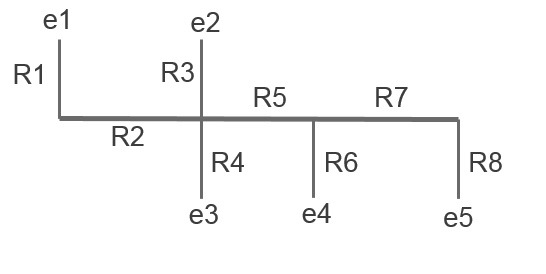
pathLength vs Length in EM report file
Length: parasitic resistor length, which is set by
emirutil reportLength=true
pathlength: Blech length is also known as "Short length" or "Path
length", and can be explained as : The longest and continuous
centerline path from edge to edge among the connected wire
shapes on the same metal layer.
For all resistors falling on this shape, same
pathLength is reported.
After the longest path in shape has been determined the tool applies
the same blech length to all the resistor falling on that shape.
This resistor length is NOT used in EM analysis
because EM rules consider Blech length of the resistor.
where W is the wire width and L is the Blech length.
By default the tool will sum all branches of a given
metal layer. In other words the path length that will be used
to look up the EM density limit is :
To enable EMIR in PSS, you have to enable DC and/or Tran simulation
simultaneously. Two or more binary results file should be generated and
select the file based file name or configure text file in
psf directory.
(given ICADVM 18.1 ISR11, Spectre 19.1 ISR6)
StarRC
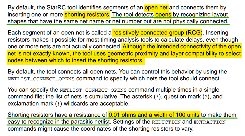
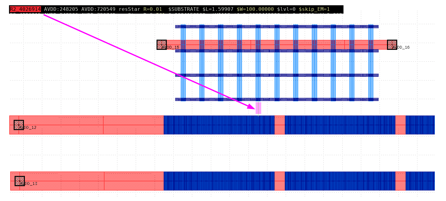
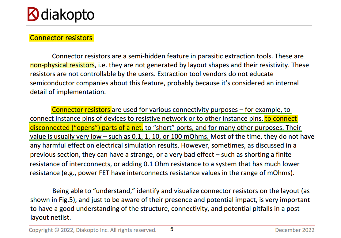
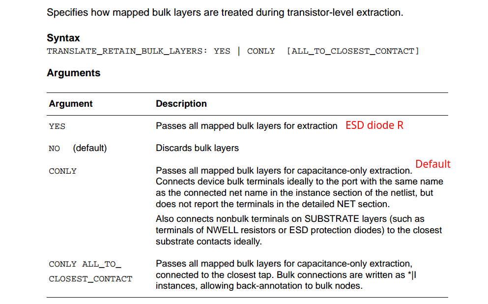
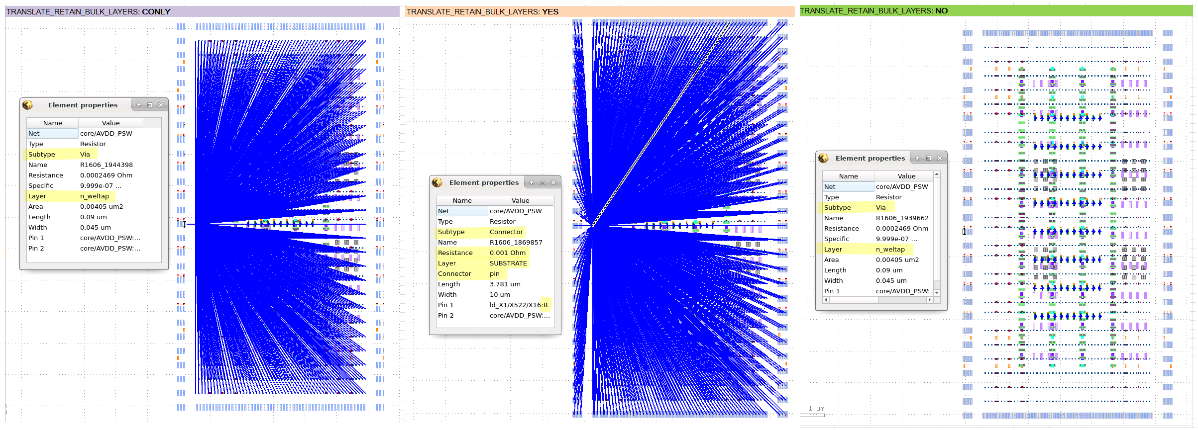
NETLIST_CONNECT_OPENS
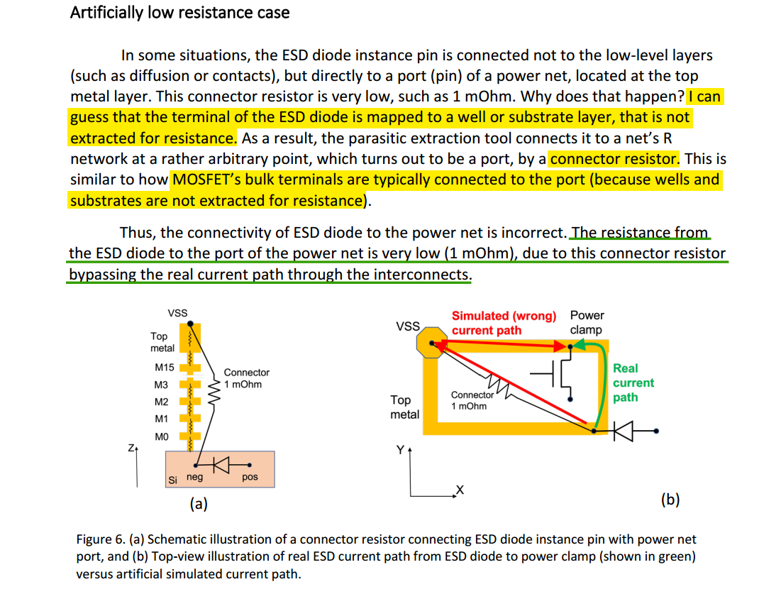
Connector resistors - non-physical
resistors (well or substrate layer, that is not extracted for
resistance)
A. B. Kahng, S. Nath and T. S. Rosing, "On potential design impacts
of electromigration awareness," 2013 18th Asia and South Pacific Design
Automation Conference (ASP-DAC), 2013, pp. 527-532, doi:
10.1109/ASPDAC.2013.6509650.
Kumar, Neeraj and Mohammad S. Hashmi. “Study, analysis and modeling
of electromigration in SRAMs.” (2014).
N. S. Nagaraj, F. Cano, H. Haznedar and D. Young, "A practical
approach to static signal electromigration analysis," Proceedings 1998
Design and Automation Conference. 35th DAC. (Cat. No.98CH36175), 1998,
pp. 572-577, doi: 10.1109/DAC.1998.724536.
Blaauw, David & Oh, Chanhee & Zolotov, Vladimir &
Dasgupta, Aurobindo. (2003). Static electromigration analysis for
on-chip signal interconnects. Computer-Aided Design of Integrated
Circuits and Systems, IEEE Transactions on. 22. 39 - 48.
10.1109/TCAD.2002.805728.
A. A. Abidi and D. Murphy, "How to Design a Differential CMOS LC
Oscillator," in IEEE Open Journal of the Solid-State Circuits
Society, vol. 5, pp. 45-59, 2025 [pdf]
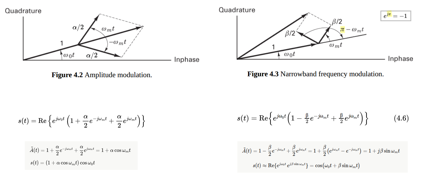
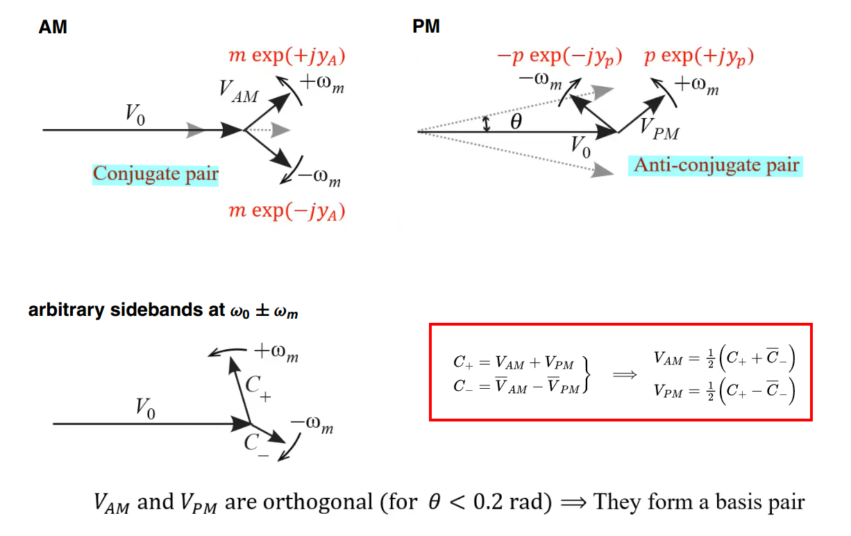
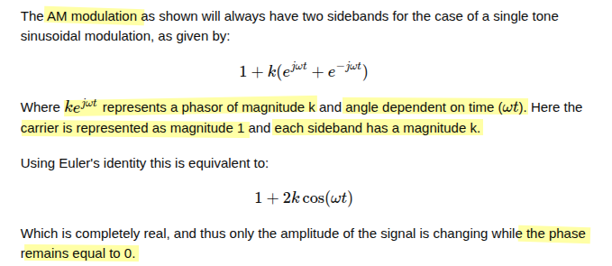
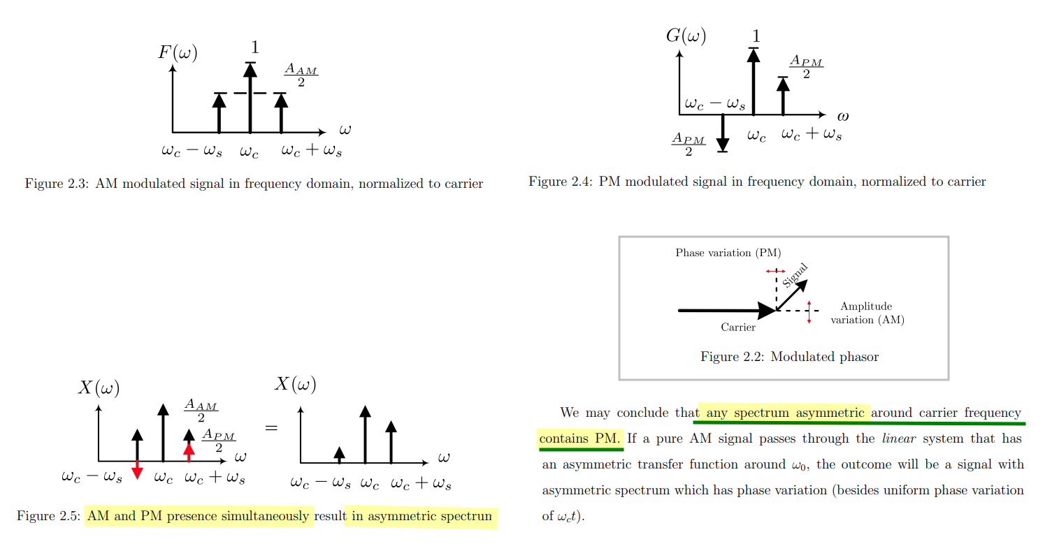
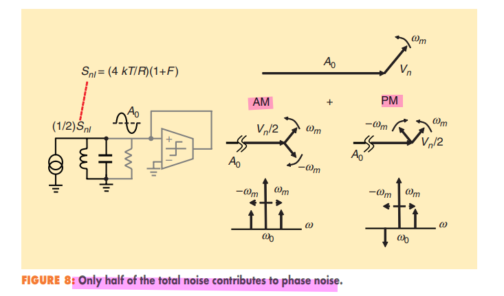
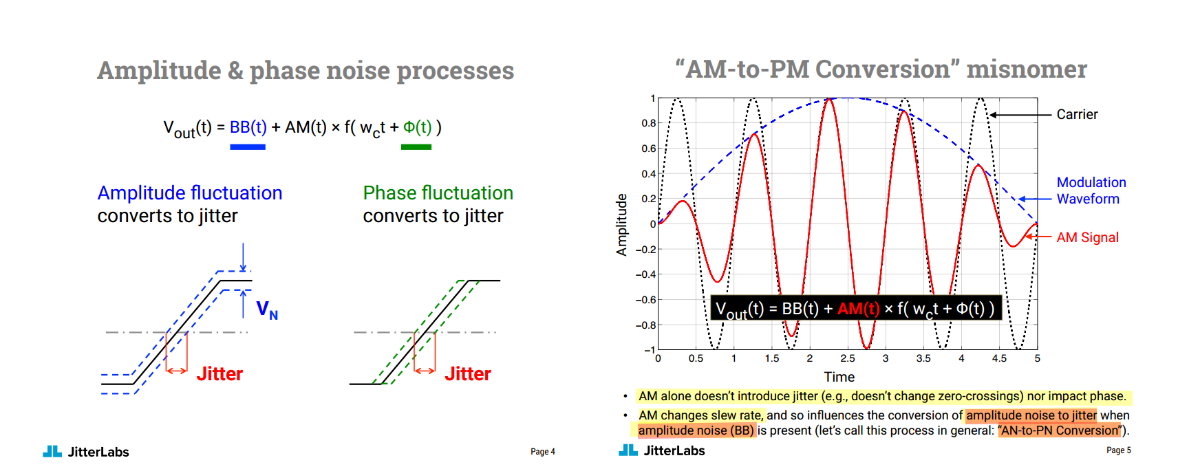
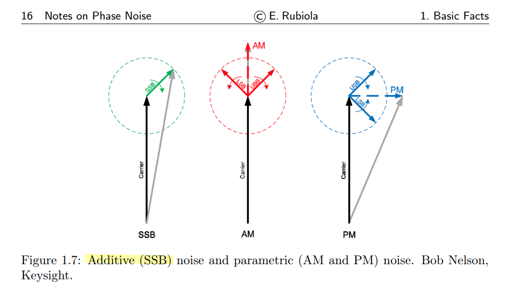
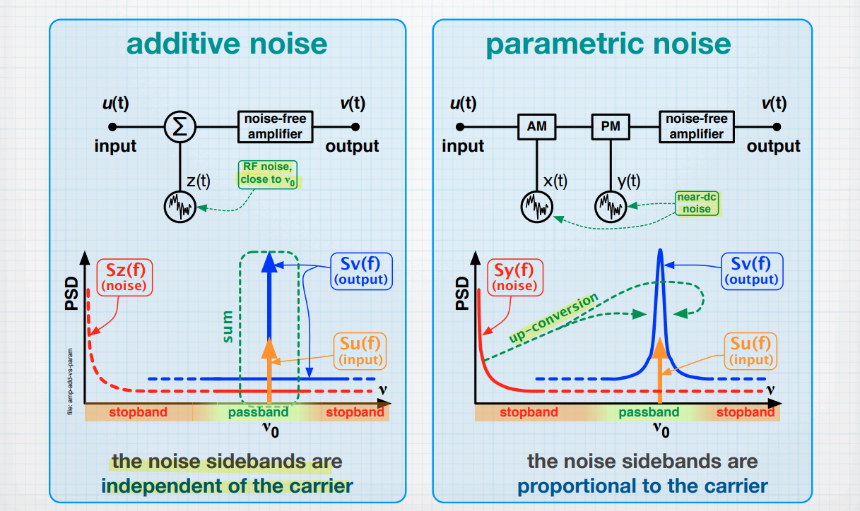
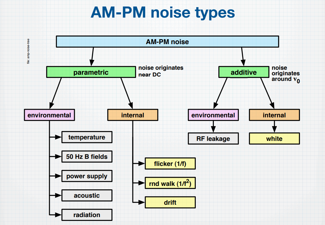
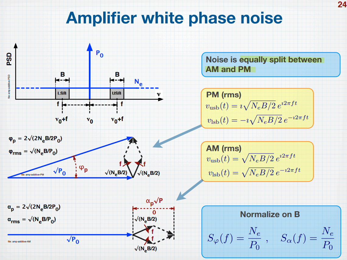
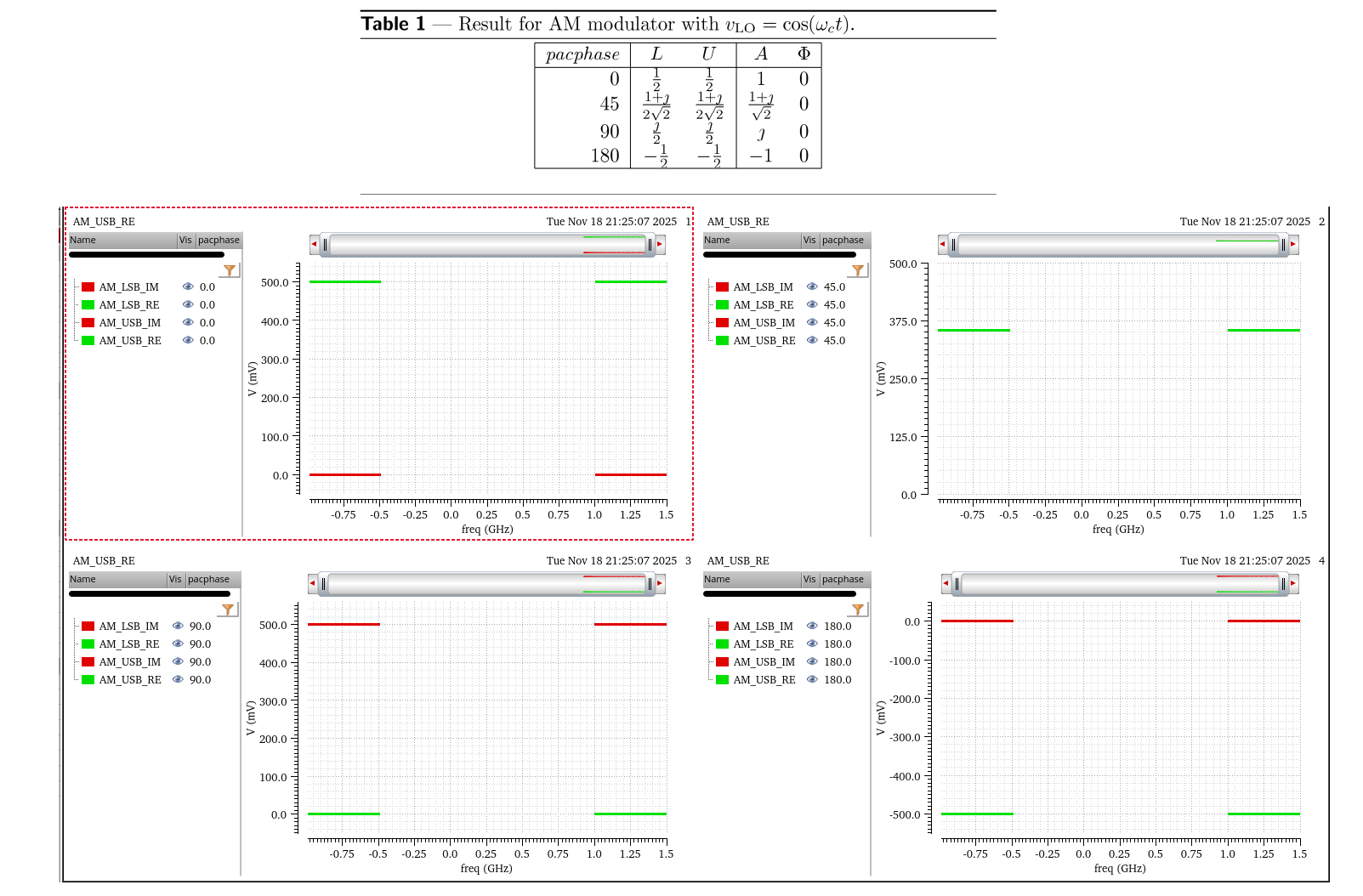
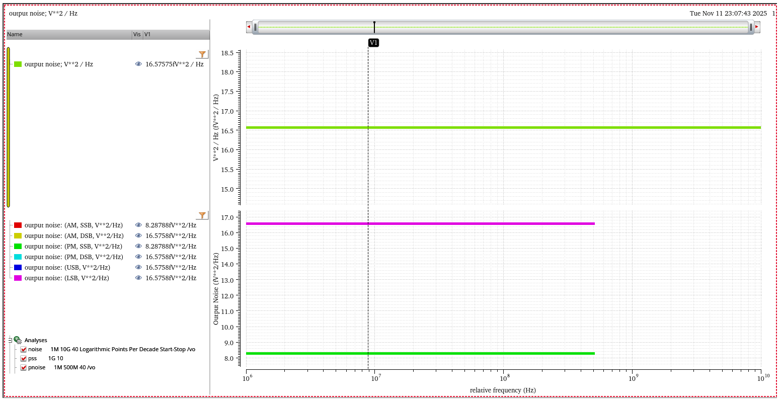
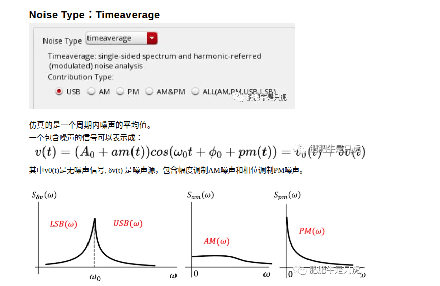
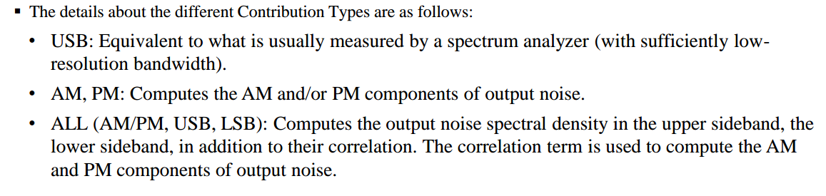
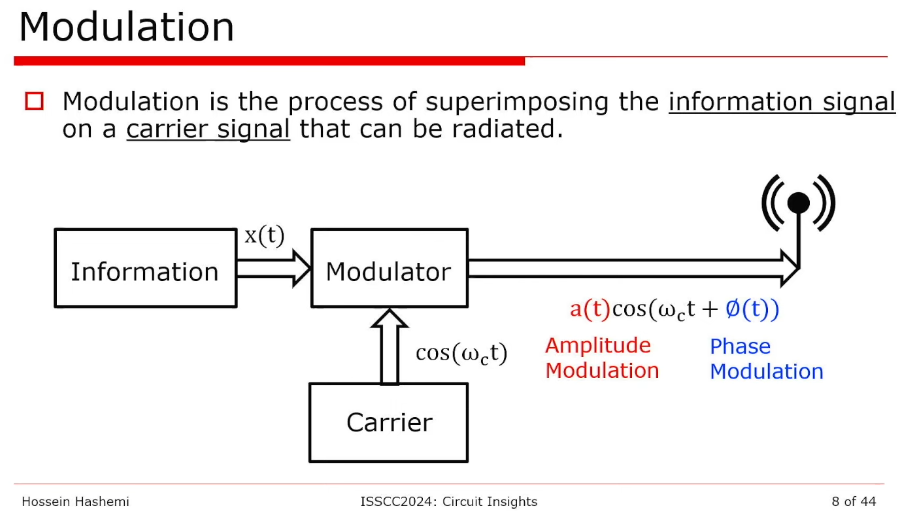
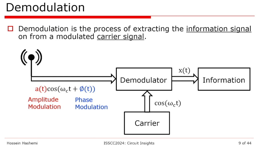
AM\[
e^{j\omega_0 t}(V_0 + V_{AM}e^{jy_A}+V_{AM}e^{-jy_A}) = V_0 e^{j\omega_0
t}\cdot \left(1+\frac{2V_{AM}}{V_0}\cos y_A\right)
\] modulate amplitude of the oscillation sinusoidally with
frequency \(\omega_m\) and depth \(m=\frac{2V_A}{V_0}\)
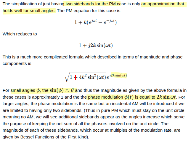
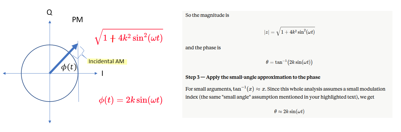
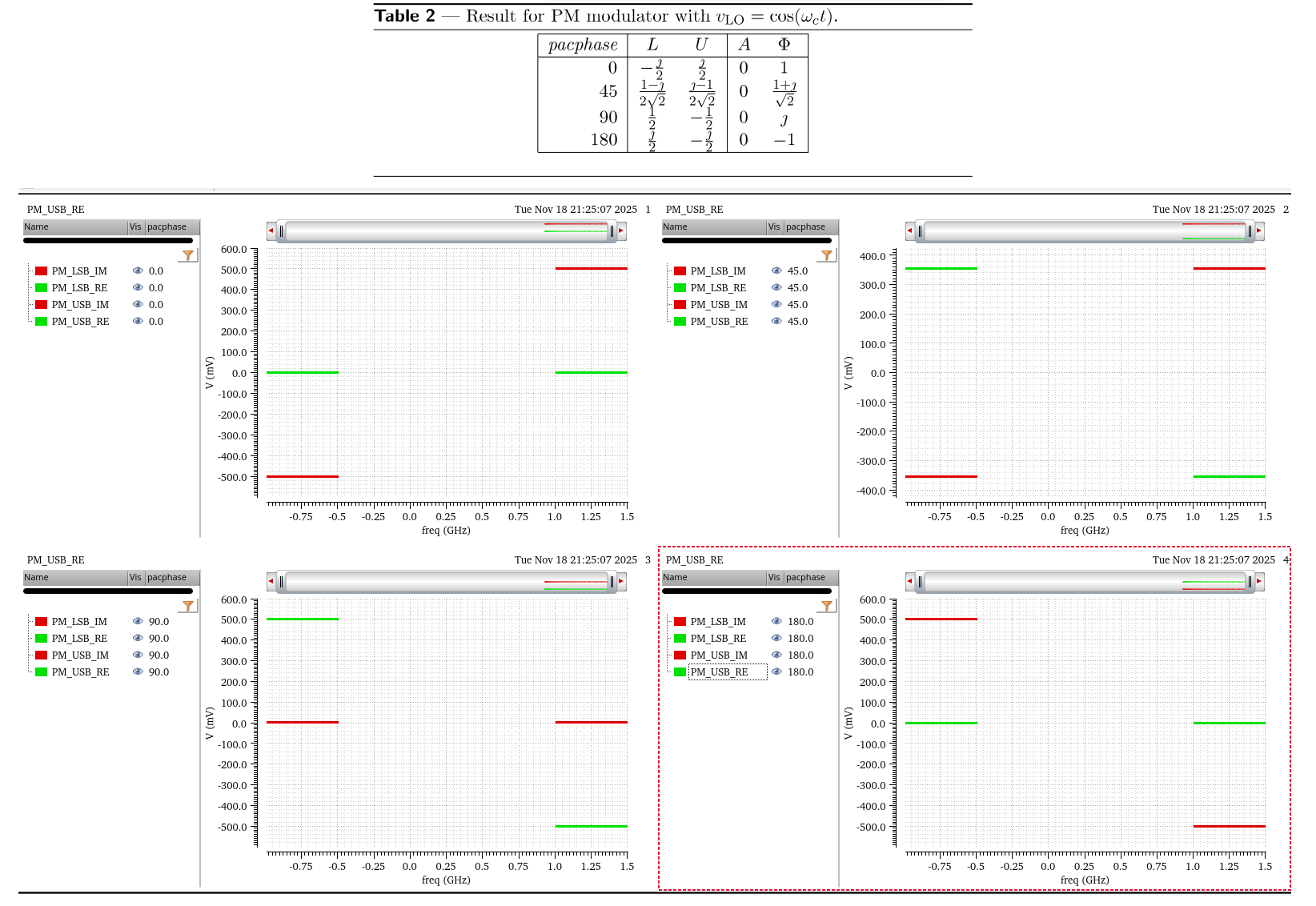
PM\[
e^{j\omega_0 t}(V_0 + V_{PM}e^{jy_P}-V_{PM}e^{-jy_P})=V_0e^{j\omega_0
t}\left(1 + j\frac{2V_{PM}}{V_0}\sin y_P\right) \approx V_0e^{j\omega_0
t}\cdot e^{j\frac{2V_{PM}}{V_0}\sin y_P}
\] modulate the phase of the oscillation with an index of
approximately \(\frac{2V_{PM}}{V_0}\)
rad
Darabi H. Radio Frequency Integrated Circuits and Systems. 2nd ed.
Cambridge University Press; 2020.
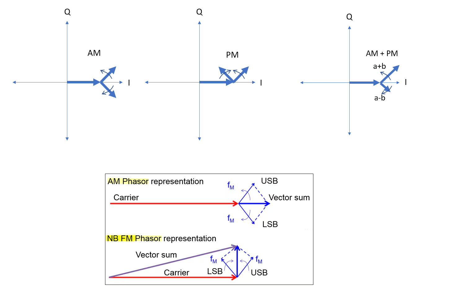
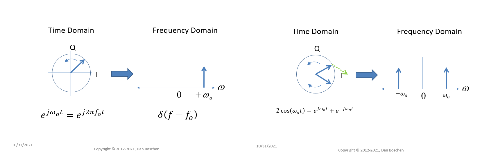
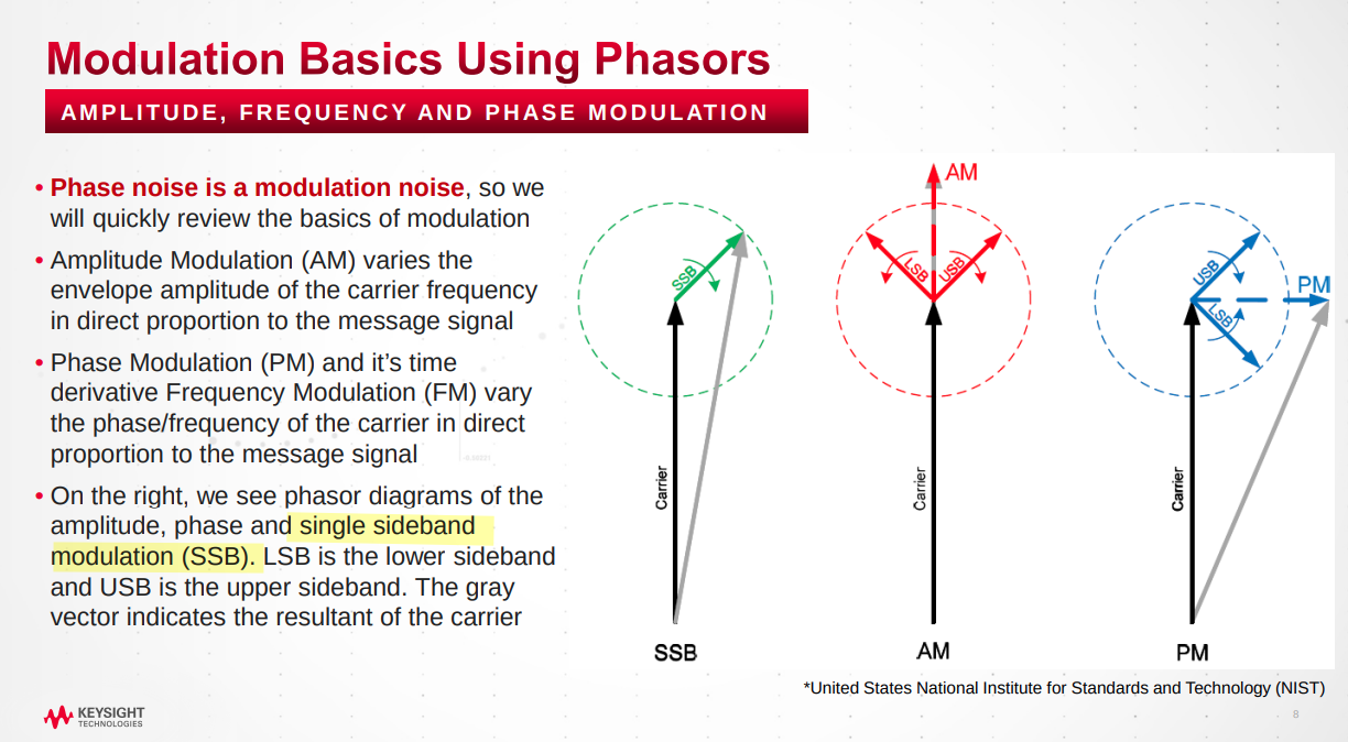
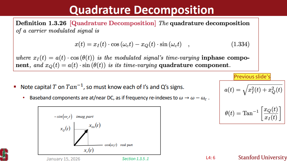
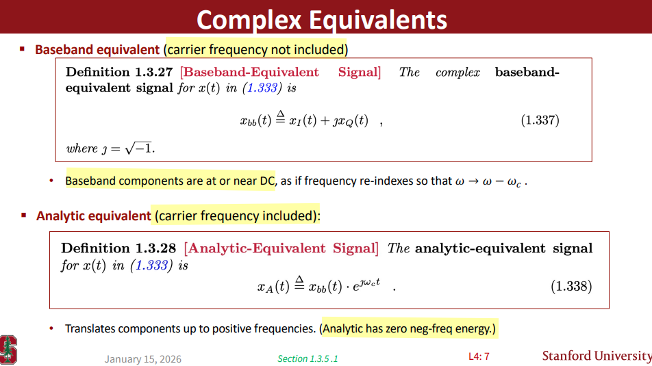
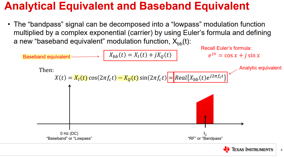
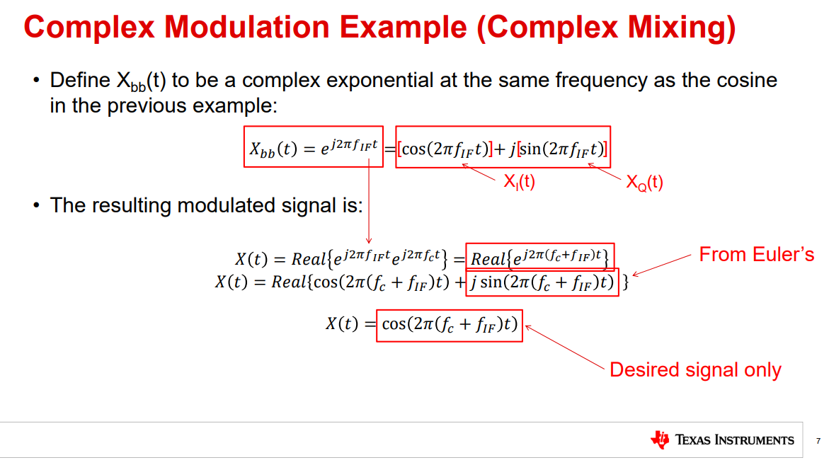
"I" is the in-phase or real axis and
"Q" is the quadrature or imaginary axis
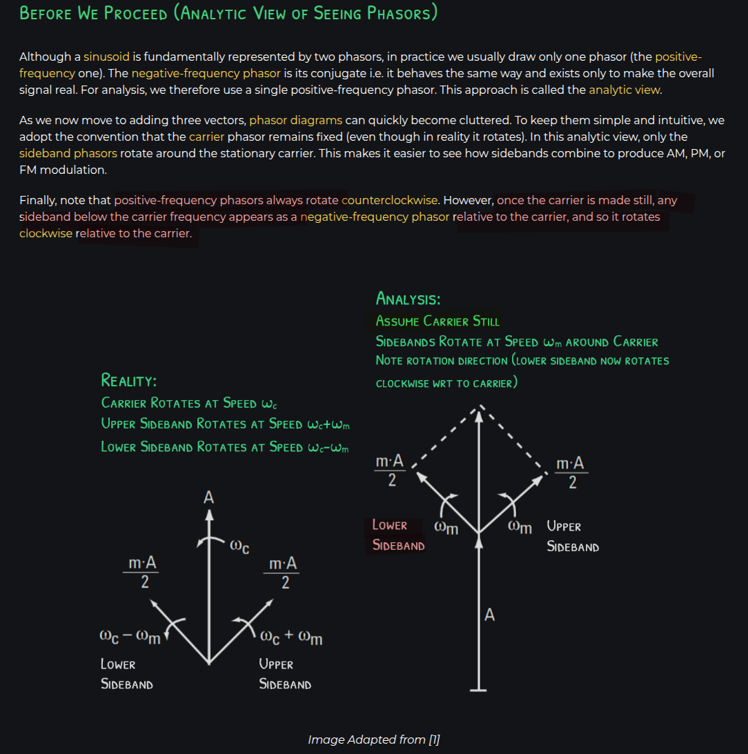
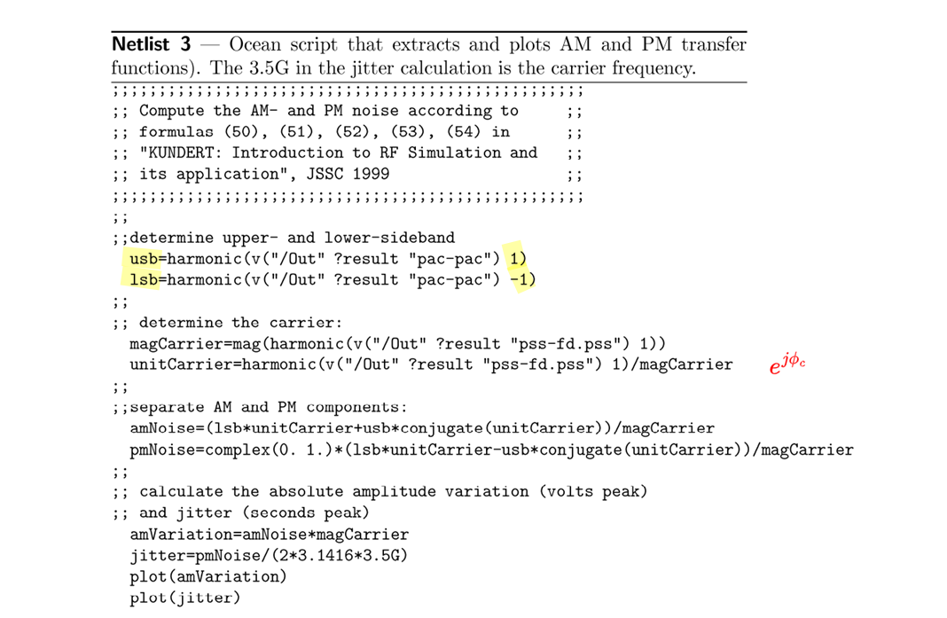
where \(X_{I,AM,USB}(t)=\cos(\omega_m
t)\) and \(X_{Q,AM,USB}(t)=\sin(\omega_m t)\); \(X_{I,AM,USB}(t)=\cos(\omega_m t)\) and
\(X_{Q,AM,USB}(t)=-\sin(\omega_m
t)\);
\(X_{I,AM,USB} = X_{I,AM,LSB}\) and
\(X_{Q,AM,USB} = -X_{Q,AM,LSB}\)
where \(X_{I,PM,USB}(t)=\cos(\omega_m
t)\) and \(X_{Q,PM,USB}(t)=\sin(\omega_m t)\); \(X_{I,PM,USB}(t)=-\cos(\omega_m t)\) and
\(X_{Q,PM,USB}(t)=\sin(\omega_m
t)\);
\(X_{I,PM,USB} = -X_{I,PM,LSB}\) and
\(X_{Q,PM,USB} = X_{Q,PM,LSB}\)
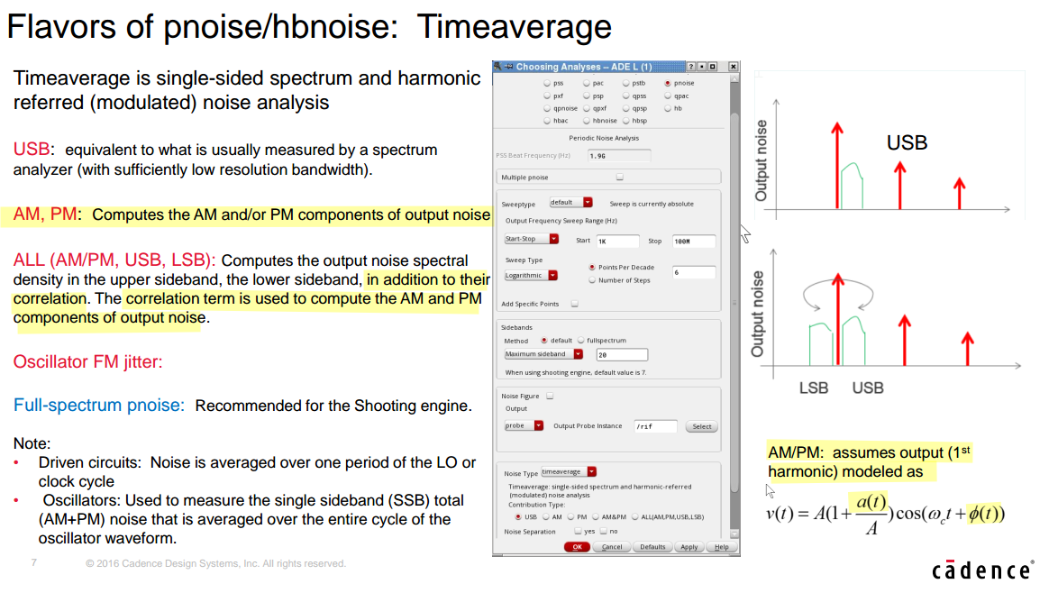
Phase Noise and Frequency Noise are not two different noise sources,
they are artifacts of the same noise, it is just a matter of what units
you want to use
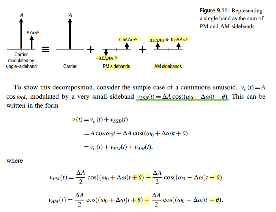
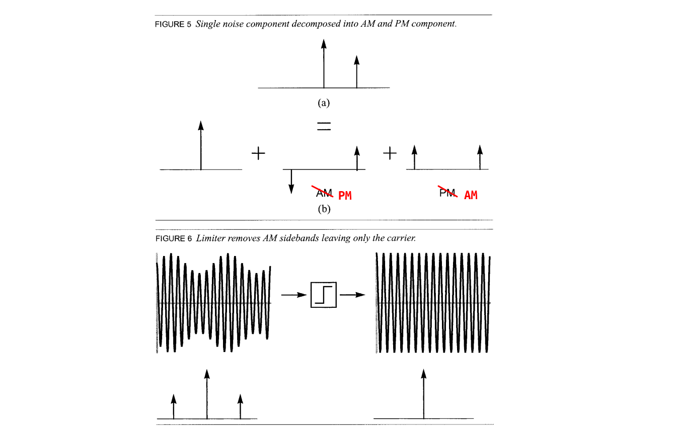
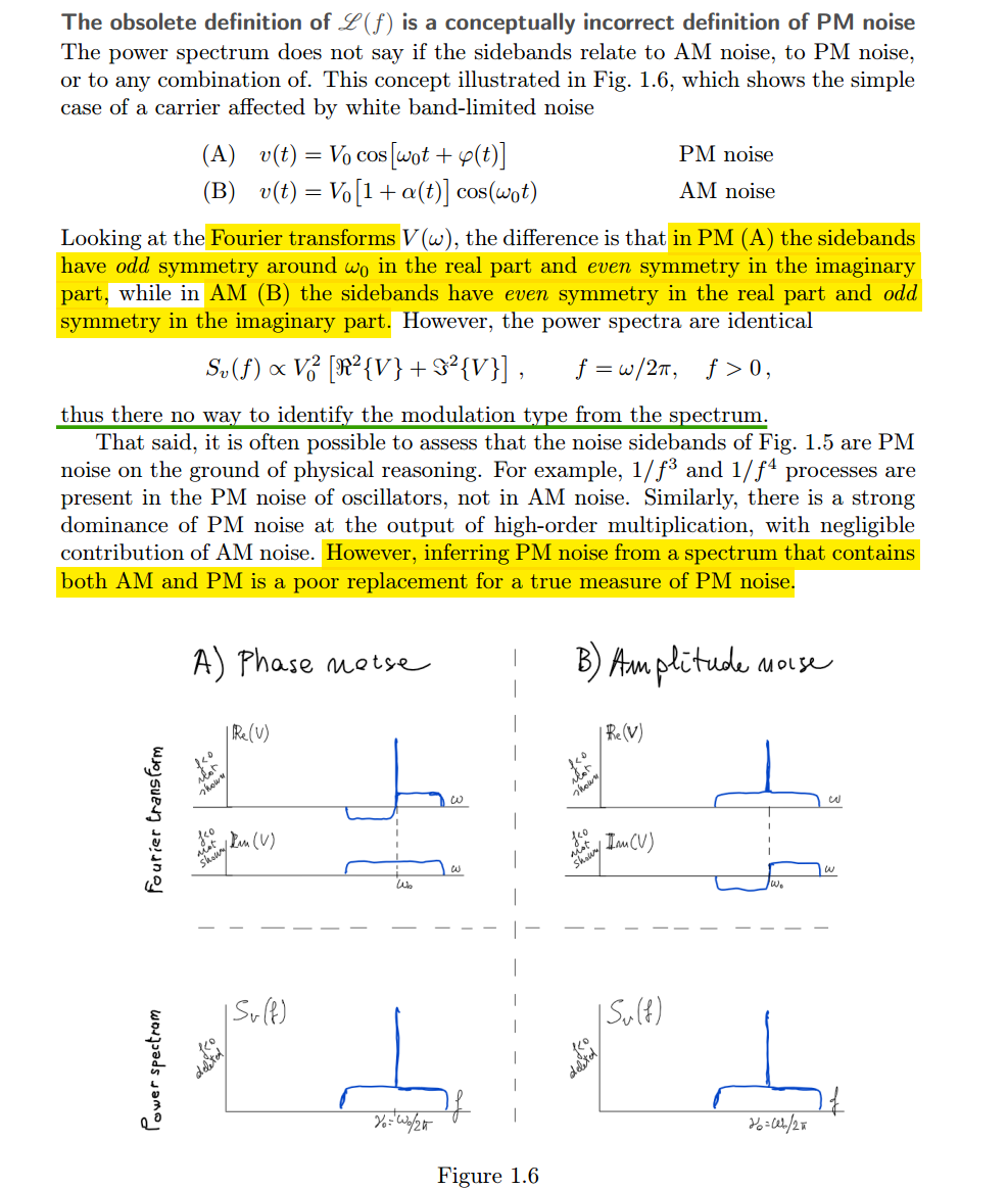
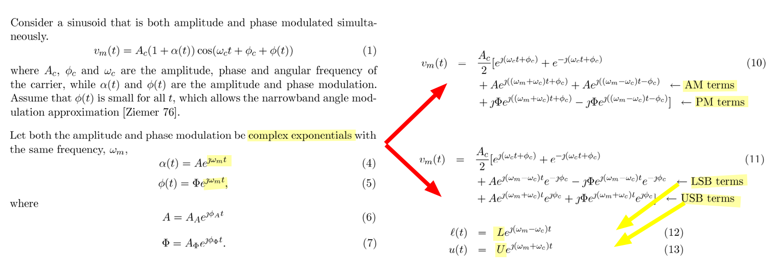
AM & PM Sidebands
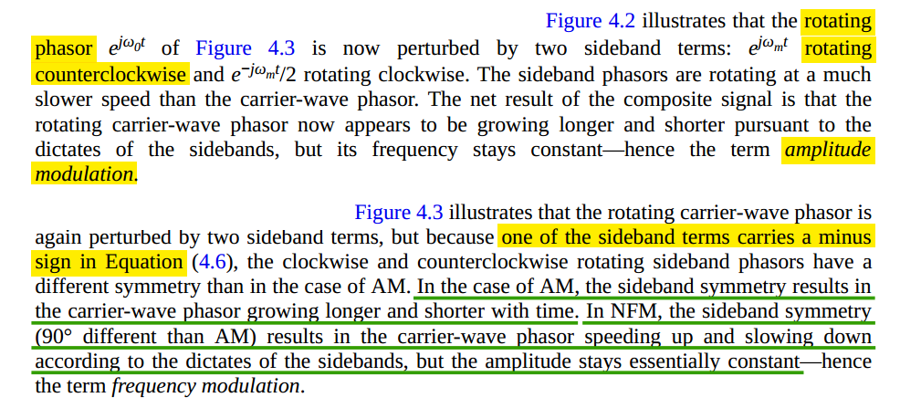
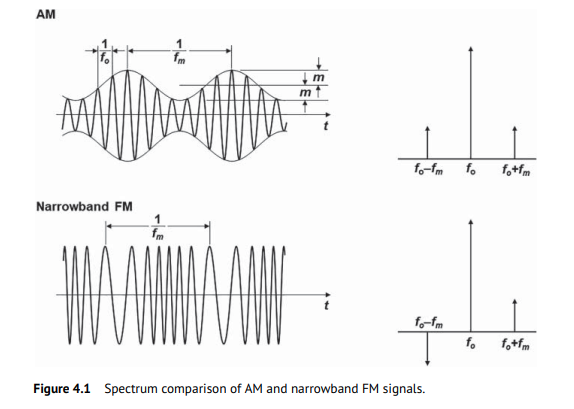
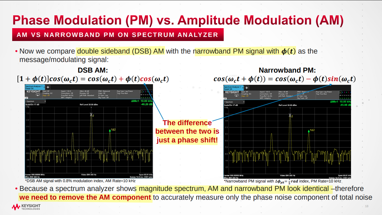
The spectrum of the narrowband FM signal is very similar to that of
an amplitude modulation (AM) signal but has the phase
reversal for the other sideband component
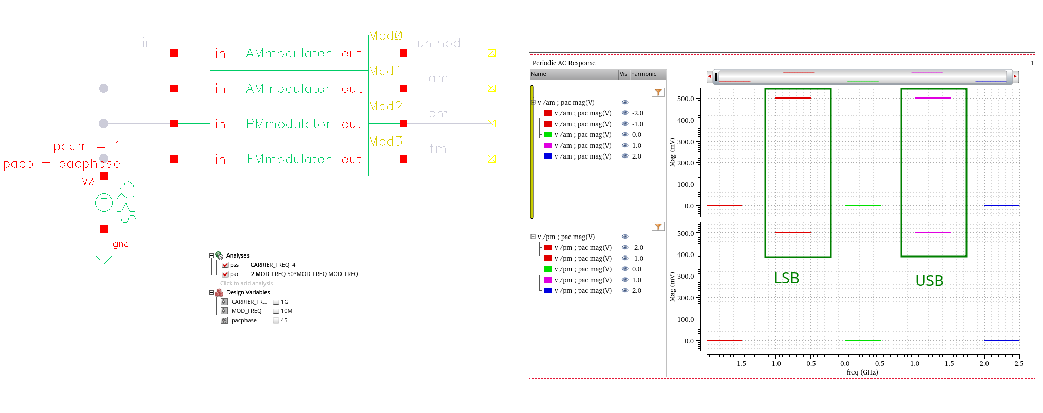
Assume the modulation frequency of PM and AM are
same, \(\omega_m\)
Bob Nelson. Phase Noise 101: Basics, Applications and Measurements
[[https://www.qsl.net/ab4oj/test/docs/20180720_KEE7_PhaseNoise.pdf])https://www.qsl.net/ab4oj/test/docs/20180720_KEE7_PhaseNoise.pdf]
Hegazi, Emad, Asad Abidi, and Jacob Rael. The Designer's Guide to
High-purity Oscillators. [New York]: Kluwer Academic Publishers,
2005. [pdf]
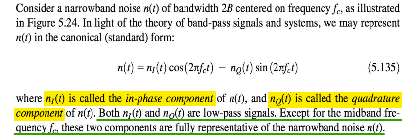
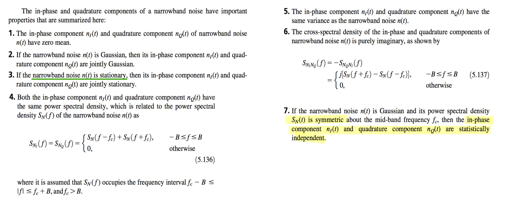
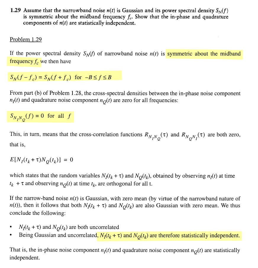
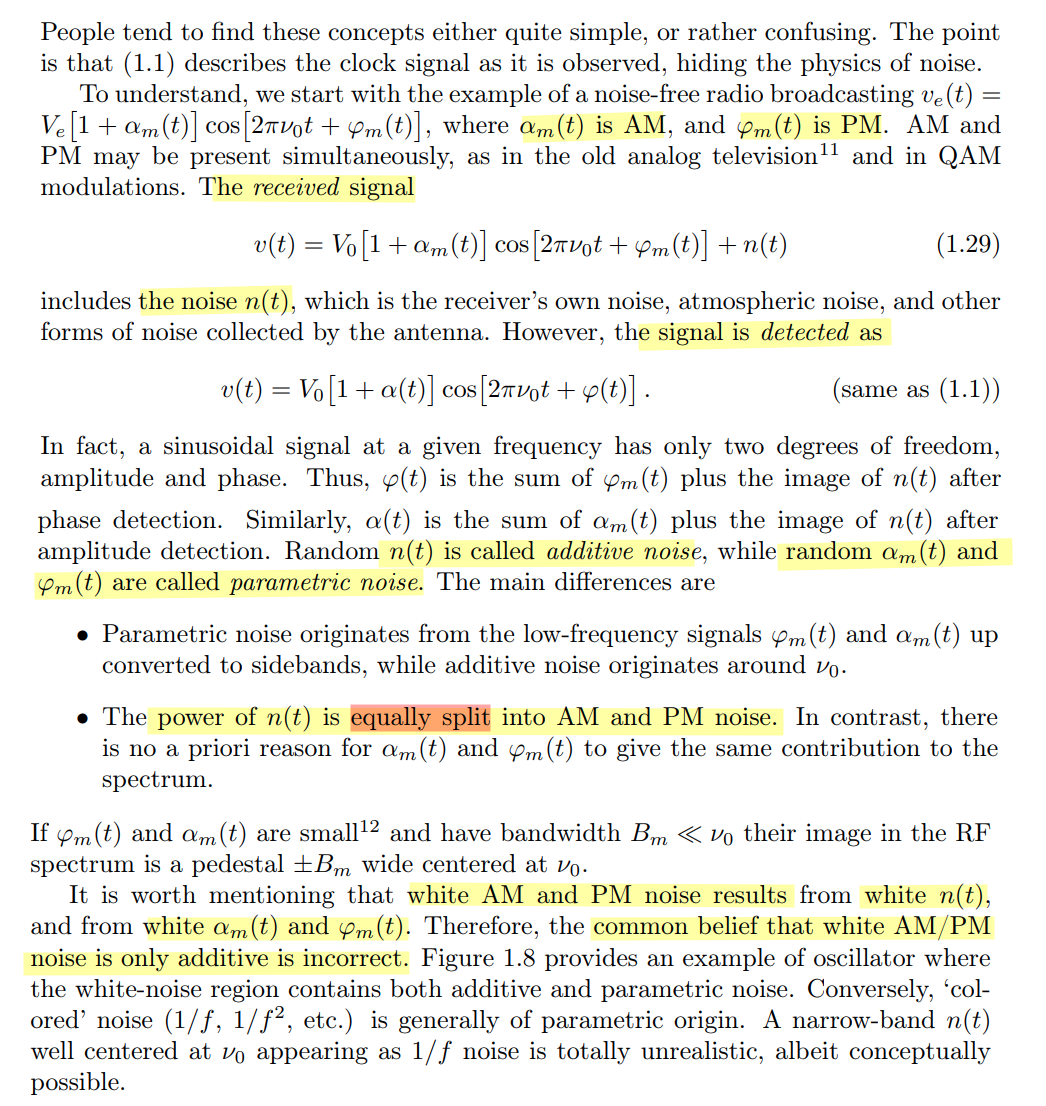
If the narrowband noise \(n(t)\) is
Gaussian and its power spectral density \(S_N
(t )\) is symmetric about the mid-band frequency
\(f_c\), then the in-phase
component\(n_I(t)\) and
quadrature component\(n_Q(t)\) are statistically
independent
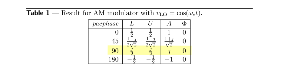
For AM & pacphase=90deg, complex
exponentials with frequency \(\omega_m\)\[
\alpha_+(t) = je^{j\omega_m t} = e^{j(\omega_mt+\pi/2)}
\] where \(A_+=j\)
Then, the complex exponentials with frequency \(-\omega_m\) shall be \[
\alpha_-(t) = [\alpha_+(t)]^* = -je^{-j\omega_m t} =
e^{-j(\omega_mt+\pi/2)}
\] where \(A_-=A_+^* =-j\)
U. L. Rohde, A. K. Poddar and A. M. Apte, "Getting Its Measure:
Oscillator Phase Noise Measurement Techniques and Limitations," in
IEEE Microwave Magazine, vol. 14, no. 6, pp. 73-86, Sept.-Oct.
2013 [https://sci-hub.jp/10.1109/MMM.2013.2269860]
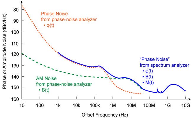
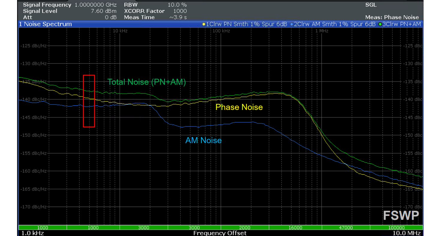
The three most widely adopted techniques are direct
spectrum, phase detector, and
two-channel cross-correlation.
While the direct spectrum technique measures phase noise with the
existence of the carrier signal, the other two remove the carrier
(demodulation) before phase noise is measured.
Though direct spectrum technique method may not be useful
for measuring very close-in phase noise to a drifting carrier,
it is convenient for qualitative quick evaluation on sources with
relatively high noise
1 2 3 4 5 6 7 8 9
import numpy as np
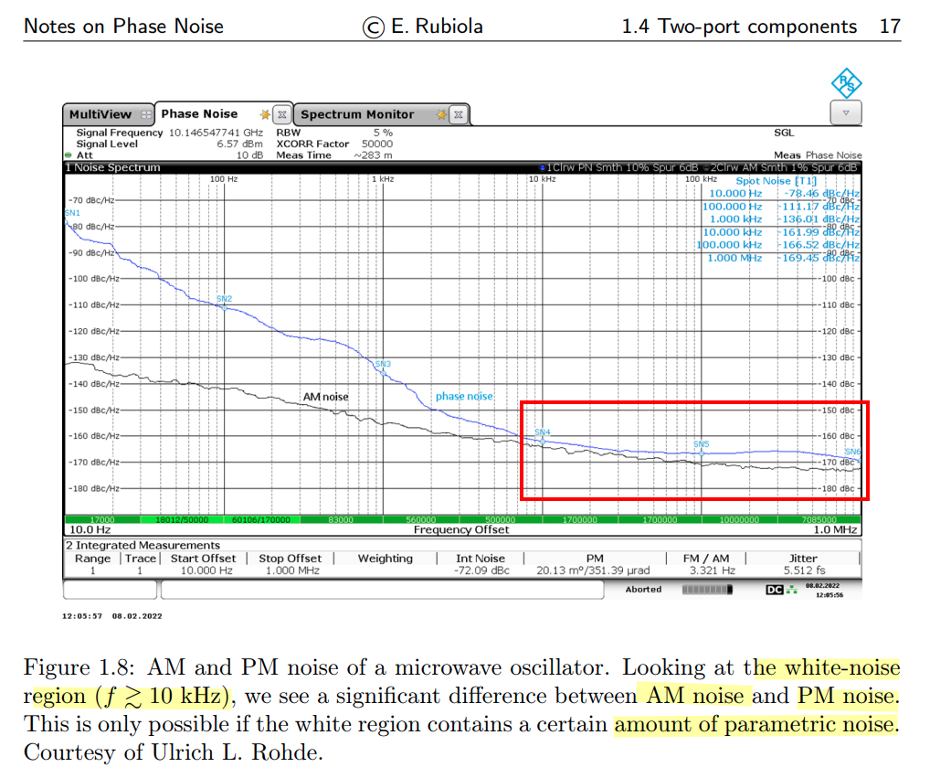
# at 5KHz n_pm = -140# dBc n_am = -142# dBc
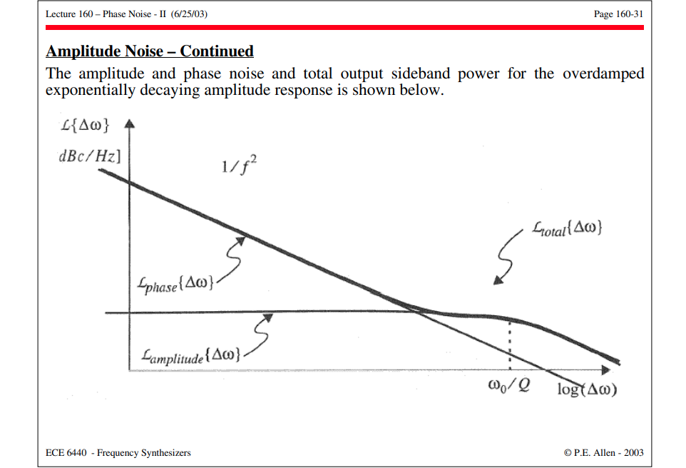
# calculate the total noise by PM + AM n_tot = 10*np.log10(10**(n_pm / 10) + 10**(n_am / 10)) print(n_tot) # -137.8755739720566
two measurements are made: the power of the carrier
and the power spectral density (PSD) of the oscillator noise at
a specified offset frequency and referenced to the carrier
power
A swept spectrum analyzer never displays the true PSD; it displays
the input spectrum convolved with the RBW filter
The carrier is measured once with a comfortably wide RBW — a CW peak
level is independent of RBW as long as the line fits inside the
filter
then each offset region is measured in segments with its own narrow,
offset-scaled RBW, normalized to 1 Hz
The classical definition is convenient when measuring phase noise
with a spectrum analyzer, but it combines both amplitude and
phase noise effects. It also has limitations for signals that
have high phase noise.
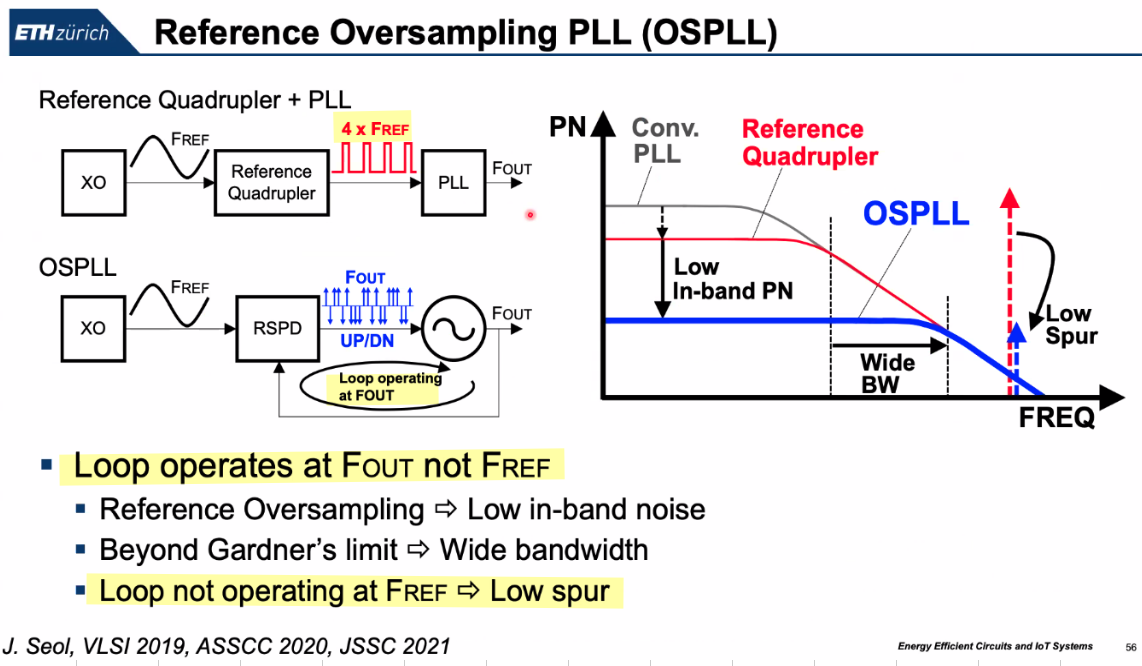
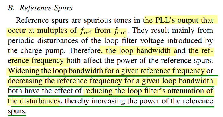
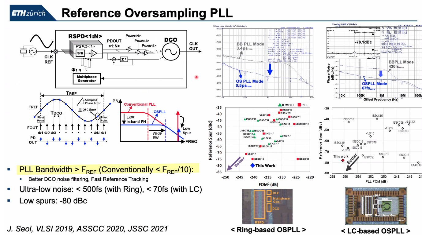
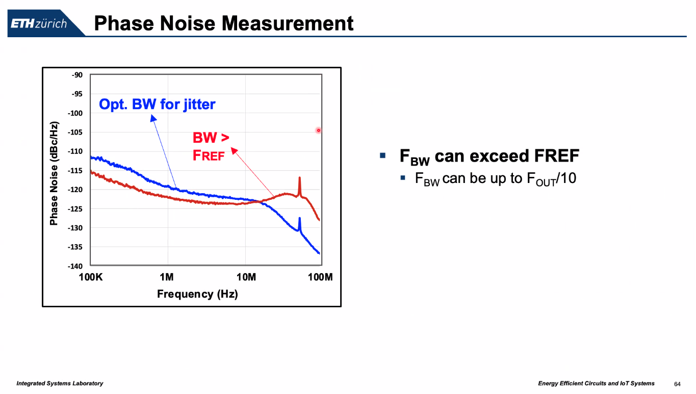
J. -H. Seol, K. Choo, D. Blaauw, D. Sylvester and T. Jang, "Reference
Oversampling PLL Achieving −256-dB FoM and −78-dBc Reference Spur," in
IEEE Journal of Solid-State Circuits, vol. 56, no. 10, pp.
2993-3007, Oct. 2021 [https://sci-hub.se/10.1109/JSSC.2021.3089930]
K. J. Wang, A. Swaminathan and I. Galton, "Spurious Tone Suppression
Techniques Applied to a Wide-Bandwidth 2.4 GHz Fractional-N PLL," in
IEEE Journal of Solid-State Circuits, vol. 43, no. 12, pp.
2787-2797, Dec. 2008 [https://sci-hub.se/10.1109/JSSC.2008.2005716]
Frequency Divider
Gunnman, Kiran, and Mohammad Vahidfar. Selected Topics in RF,
Analog and Mixed Signal Circuits and Systems. Aalborg: River
Publishers, 2017
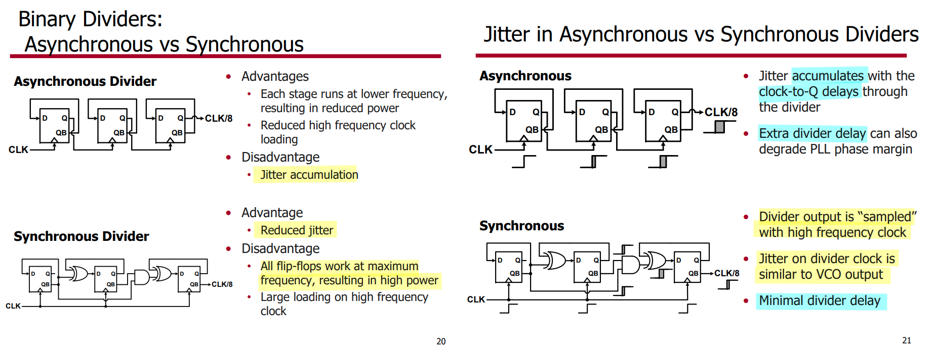
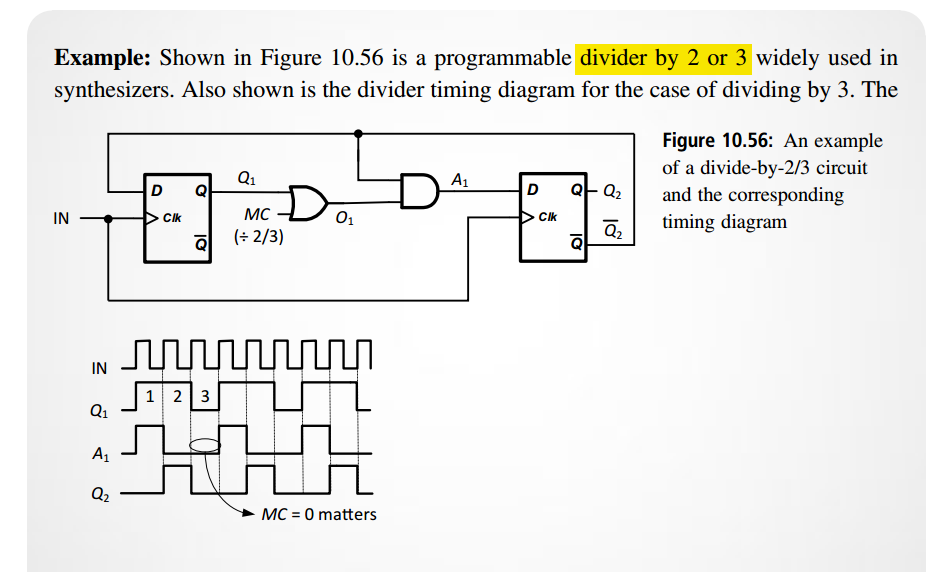
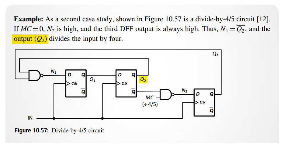
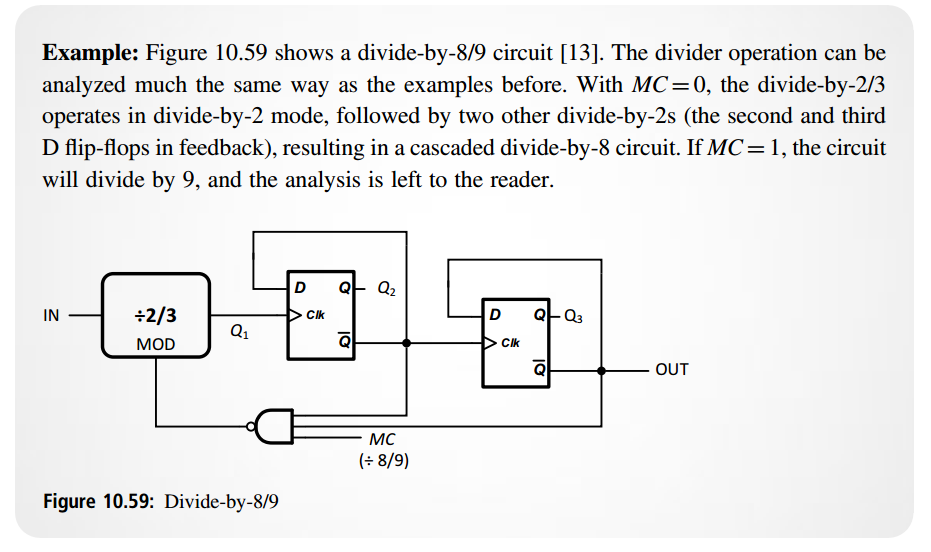
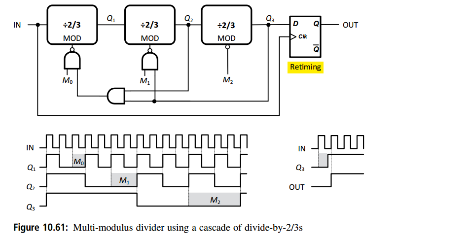
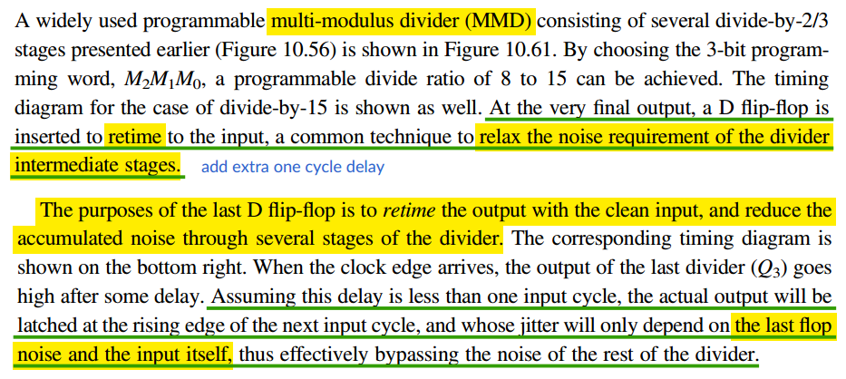
Multi-modulus divider using a cascade of divide-by-2/3s
extra one cycle
delay vs reducing accumulated
noise from the last retiming DFF
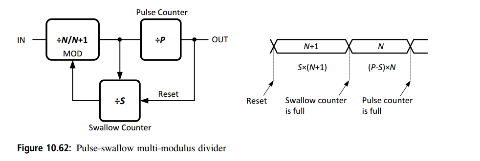
Pulse-swallow multi-modulus
divider
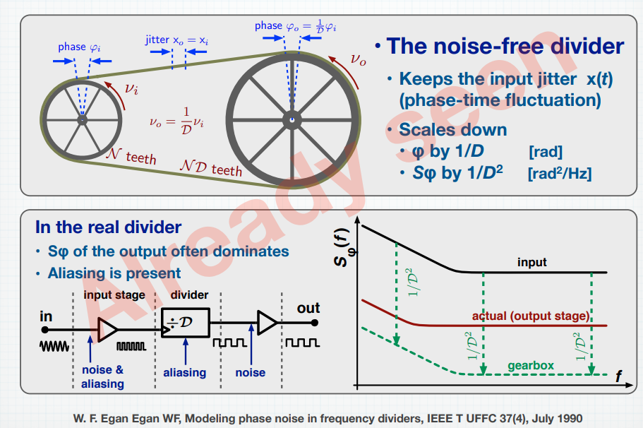
Noise in dividers (jitter
generation)
S. Levantino, L. Romano, S. Pellerano, C. Samori and A. L. Lacaita,
"Phase noise in digital frequency dividers," in IEEE Journal of
Solid-State Circuits, vol. 39, no. 5, pp. 775-784, May 2004 [https://sci-hub.se/10.1109/JSSC.2004.826338]
Lacaita, Andrea Leonardo, Salvatore Levantino, and Carlo Samori.
Integrated frequency synthesizers for wireless systems.
Cambridge University Press, 2007.
W. F. Egan, "Modeling phase noise in frequency dividers," in IEEE
Transactions on Ultrasonics, Ferroelectrics, and Frequency Control, vol.
37, no. 4, pp. 307-315, July 1990 [https://sci-hub.se/10.1109/58.56498]
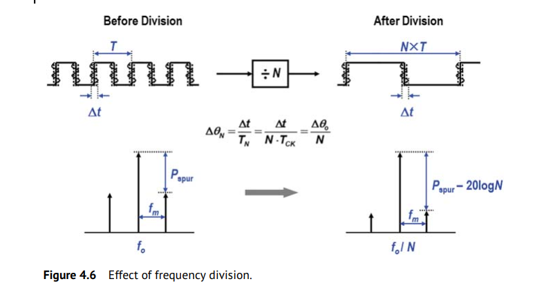
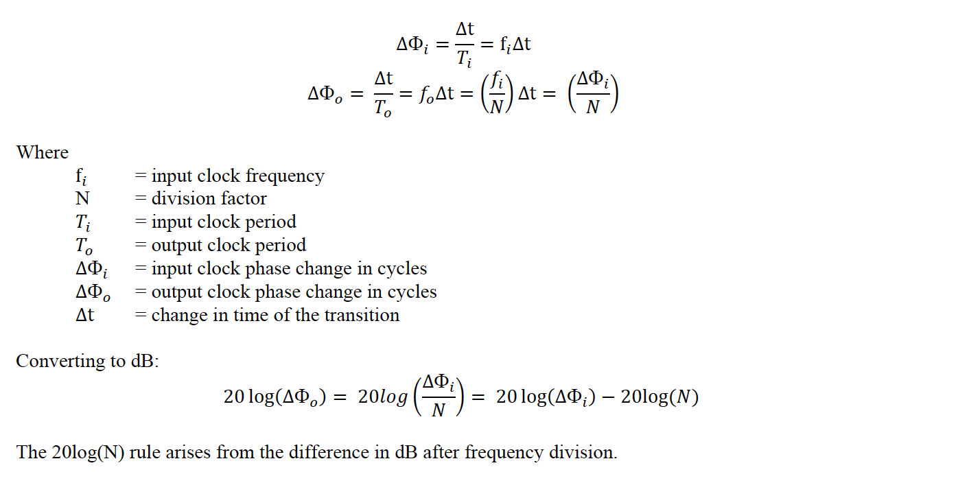
Multiplying the frequency of a signal by a factor of N using an
ideal frequency multiplier increases the phase noise of
the multiplied signal by \(20\log(N)\)
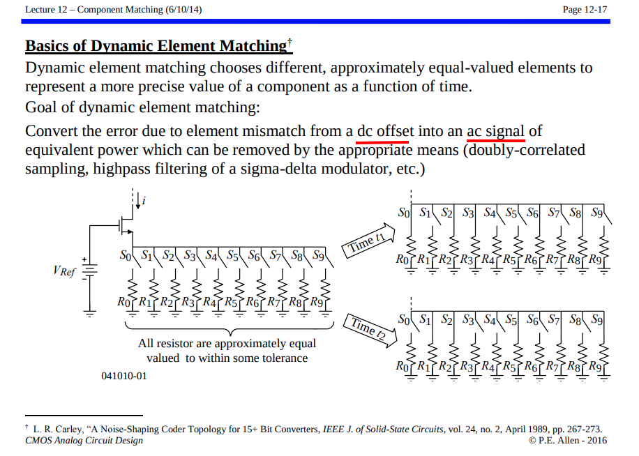
dB.
Similarly dividing a signal frequency by \(N\) reduces the phase noise of the output
signal by \(20\log(N)\) dB
The sideband offset from the carrier in the frequency
multiplied/divided signal is the same as for the original signal.
\(20\log (N)\)
Rule
If the carrier frequency of a clock is divided down by a factor of
\(N\) then we expect the phase noise to
decrease by \(20\log(N)\).The primary
assumption here is a noiseless conventional digital
divider.
The \(20\log(N)\) rule only applies
to phase noise and not integrated phase noise or phase
jitter. Phase jitter should generally measure about the
same.
What About Phase Jitter?
We integrate SSB phase noise L(f) [dBc/Hz] to
obtain rms phase jitter in seconds as follows for “brick wall”
integration from f1 to f2 offset frequencies in Hz and where f0 is the
carrier or clock frequency.
Note that the rms phase jitter in seconds is inversely proportional
to f0. When frequency is divided down, the phase noise, L(f),
goes down by a factor of 20log(N). However, since the frequency goes
down by N also, the phase jitter expressed in units of time is
constant.
Therefore, phase noise curves, related by 20log(N), with the same
phase noise shape over the jitter bandwidth, are expected to
yield the same phase jitter in seconds.
with \(M_{ref}\), the number of
reference clock cycles \[
A\cdot \frac{T_{ref}}{N} + B\cdot \frac{T_{ref}}{N+1} = M_{ref} T_{ref}
\qquad N_{vco} = A +B
\]
spurs are carrier or clock frequency spectral
imperfections measured in the frequency domain just like phase noise.
However, unlike phase noise they are discrete frequency
components.
Spurs are deterministic
Spur power is independent of bandwidth
Spurs contribute bounded peak jitter in the time domain
Sources of Spurs:
External (coupling from other noisy block) Supply, substrate, bond
wires, etc.
Internal (int-N/fractional-N operation)
Frac spur: Fractional divider (multi-modulus and
frequency accumulation)
the frequency resolution, is equal to the reference
frequency, meaning that only integer multiples of the reference
frequency can be synthesized
Stability requirements limit the loop bandwidth to about
one tenth of the reference frequency; therefore
decreasing the reference frequency increases the settling time as
the loop bandwidth also has to be decreased
a reduced loop bandwidth allows less suppression of the VCO’s
inherent phase noise
Another drawback of the integer-N PLL is the trade-off
between phase noise and settling time when the divider ratio
becomes large (The contributions to the output phase noise of
almost all PLL building blocks, except the VCO, are multiplied
by the division ratio)
if a small reference frequency is chosen, the reference spur
in the output phase noise is located at a smaller offset
frequency
Fractional-N
Dither Feedback Divider Ratio by a delta-sigma
modulator
Frequency Accumulation
Switched Capacitor Banks
Q: why \(R_b\) ?
A: TODO 📅
Hu, Yizhe. "Flicker noise upconversion and reduction mechanisms in
RF/millimeter-wave oscillators for 5G communications." PhD diss.,
2019.
S. D. Toso, A. Bevilacqua, A. Gerosa and A. Neviani, "A thorough
analysis of the tank quality factor in LC oscillators with switched
capacitor banks," Proceedings of 2010 IEEE International Symposium
on Circuits and Systems, Paris, France, 2010, pp. 1903-1906
False locking
TODO 📅
divider failure
even-stage ring oscillator ( multipath ring oscillators)
DLL: harmonic locking, stuck locking
clock edge impact
ck1 is div2 of ck0
edge of ck0 is affected differently by ck1
edge of ck1 is affected equally by ck0
Why Type 2 PLL ?
Type: # of integrators within the loop
Order: # of poles in the closed-loop
transfer function
Type \(\leq\) Order
That is, to have a wide bandwidth, a high loop gain is required
More importantly, the type 1 PLL has the problem of a
static phase error for the change of an input
frequency
Pulse Code Modulation (PCM) is a method for digitally representing
analog signals by sampling their amplitude at regular intervals and then
encoding these samples into binary numbers
Energy/bit (pJ/b)
1mW/Gbps = 1pJ/bit
Joules are a unit of work or energy.
Watts are a unit of power which is the rate at
which energy is generated or consumed.
modulation depth
The modulation index (or
modulation depth) of a modulation scheme
describes by how much the modulated variable of the carrier signal
varies around its unmodulated level
The Nyquist rate is the minimum sample rate required
to accurately measure a signal's highest frequency. It's equal to
twice the highest frequency of the
signal
Nyquist frequency
The Nyquist frequency is the highest frequency that can be
represented without aliasing in a discrete signal. It's
equal to half the sampling frequency
Oversampling Ratio (OSR) is defined as the ratio of
the Nyquist frequency\(f_s/2\) to the signal bandwidth\(B\) given by \(\text{OSR}=f_s/2B\)
The probability distribution of the sum of two or more
independent random variables is the
convolution of their individual distributions.
Thermal noise
Thermal noise in an ideal resistor is approximately
white, meaning that its power spectral density is
nearly constant throughout the frequency spectrum.
When limited to a finite bandwidth and viewed in the time
domain, thermal noise has a nearly Gaussian amplitude
distribution
sinusoidal
steady-state and frequency response
Due to KCL and \(u(t)=e^{j\omega
t}\) and \(y(t)=H(j\omega)e^{j\omega
t}\), we have ODE:
\(H(j\omega)\) is obtained as below
\[
H(j\omega) = \frac{1}{1+j\omega}
\]
PSD Definition Variants
In the practice of engineering, it has become customary to use
slightly different variants of the PSD definition, depending on the
particular application or research field.
Two-Sided PSD, \(S_x(f)\)
this is a synonym of the PSD defined as the Fourier Transform of the
autocorrelation.
One-Sided PSD, \(S'_x(f)\)
this is a variant derived from the two-sided PSD by
considering only the positive frequency semi-axis.
To conserve the total power, the value of the
one-sided PSD is twice that of the two-sided PSD \[
S'_x(f) = \left\{ \begin{array}{cl}
0 & : \ f \geq 0 \\
S_x(f) & : \ f = 0 \\
2S_x(f) & : \ f \gt 0
\end{array} \right.
\]
Note that the one-sided PSD definition makes sense only if the
two-sided is an even function of \(f\)
If \(S'_x(f)\) is even
symmetrical around a positive frequency \(f_0\), then two additional definitions can
be adopted:
Single-Sideband PSD, \(S_{SSB,x}(f)\)
This is obtained from \(S'_x(f)\) by moving the origin of the
frequency axis to \(f_0\)\[
S_{SSB,x}(f) =S'_x(f+f_0)
\] This concept is particularly useful for describing phase or
amplitude modulation schemes in wireless communications, where \(f_0\) is the carrier frequency.
Note that there is no difference in the values of the one-sided
versus the SSB PSD; it is just a pure translation on the frequency
axis.
Double-Sideband PSD, \(S_{DSB,x}(f)\)
this is a variant of the SSB PSD obtained by considering only the
positive frequency semi-axis.
As in the case of the one-sided PSD, to conserve total power, the
value of the DSB PSD is twice that of the SSB \[
S_{DSB,x}(f) = \left\{ \begin{array}{cl}
0 & : \ f \geq 0 \\
S_{SSB,x}(f) & : \ f = 0 \\
2S_{SSB,x}(f) & : \ f \gt 0
\end{array} \right.
\]
Note that the DSB definition makes sense only if the SSB PSD is even
symmetrical around zero
Poles and Zeros of
transfer function
poles
\[
H(s) = \frac{1}{1+s/\omega_0}
\]
magnitude and phase at \(\omega_0\)
and \(-\omega_0\)\[\begin{align}
H(j\omega_0) &= \frac{1}{1+j} = \frac{1}{\sqrt{2}}e^{-j\pi/4} \\
H(-j\omega_0) &= \frac{1}{1-j} = \frac{1}{\sqrt{2}}e^{j\pi/4}
\end{align}\]
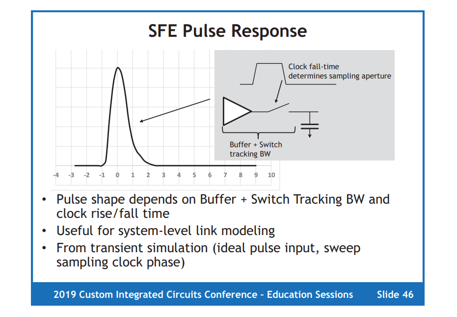

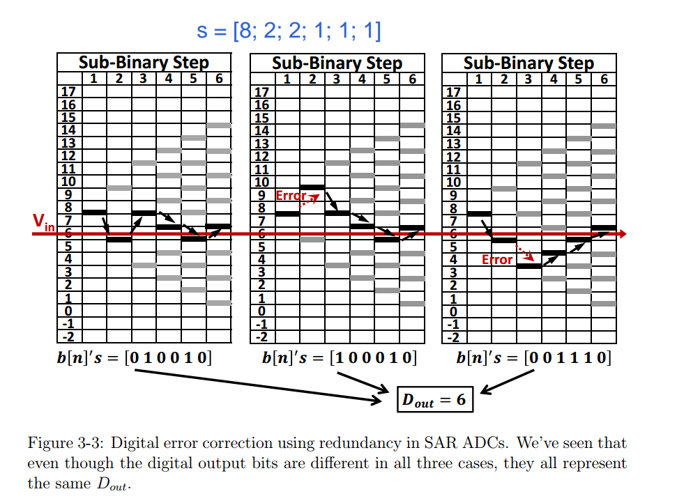

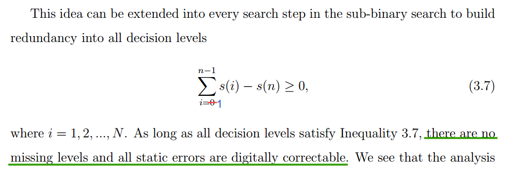
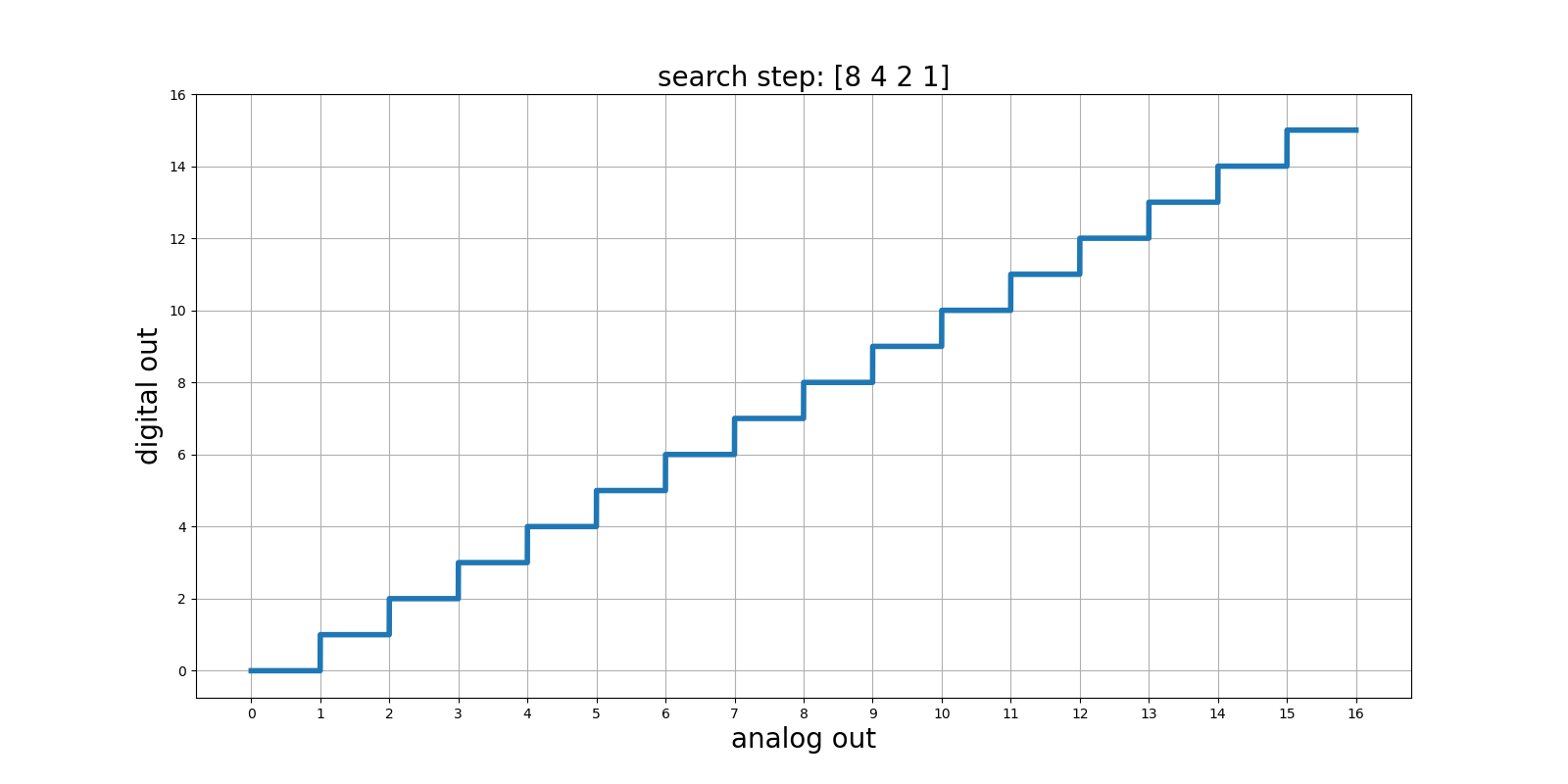
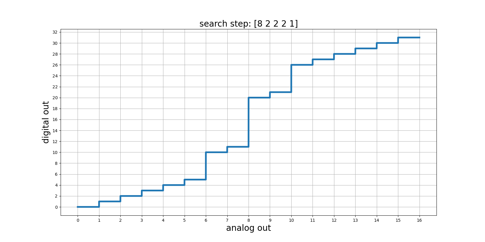
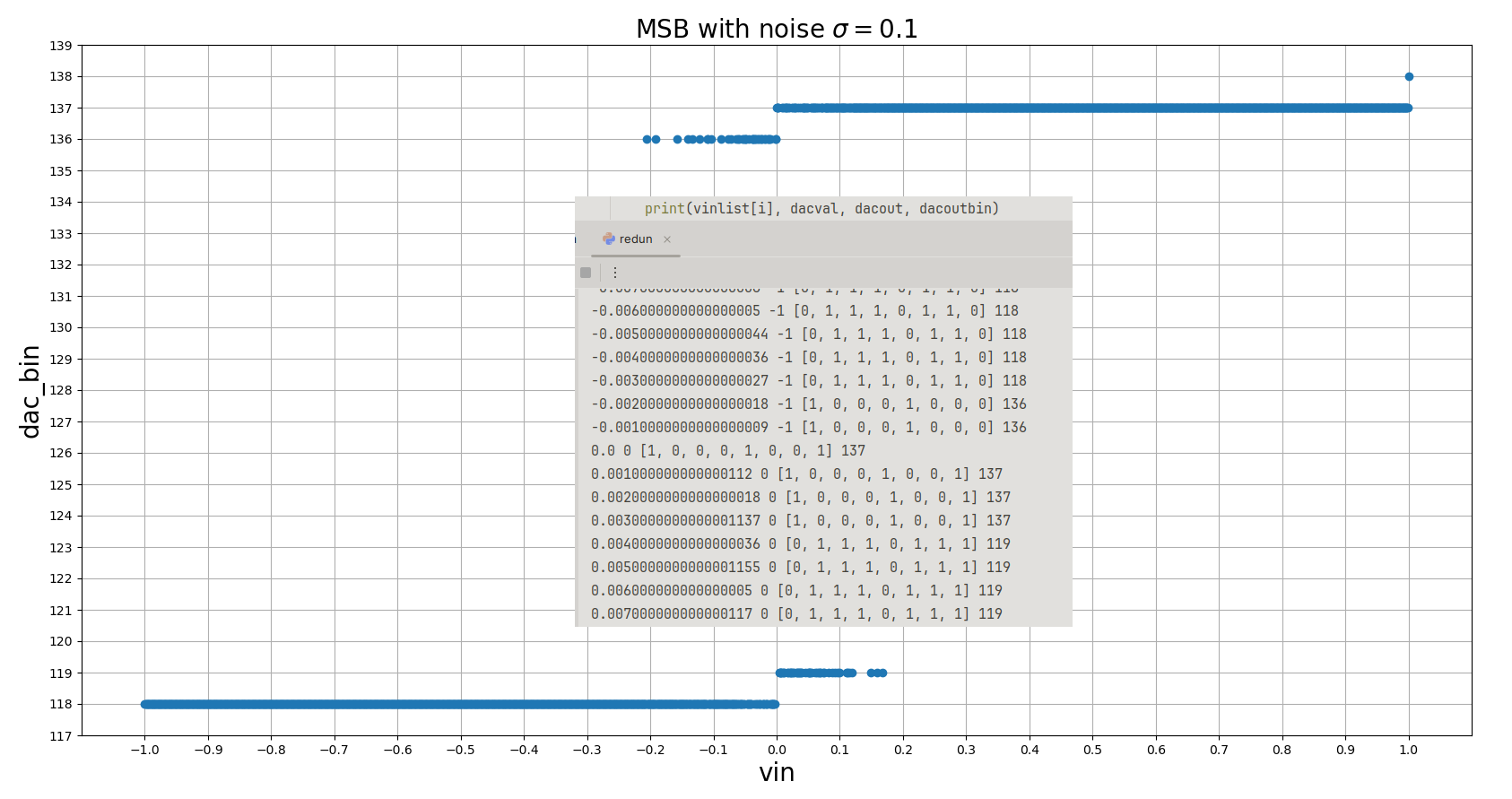
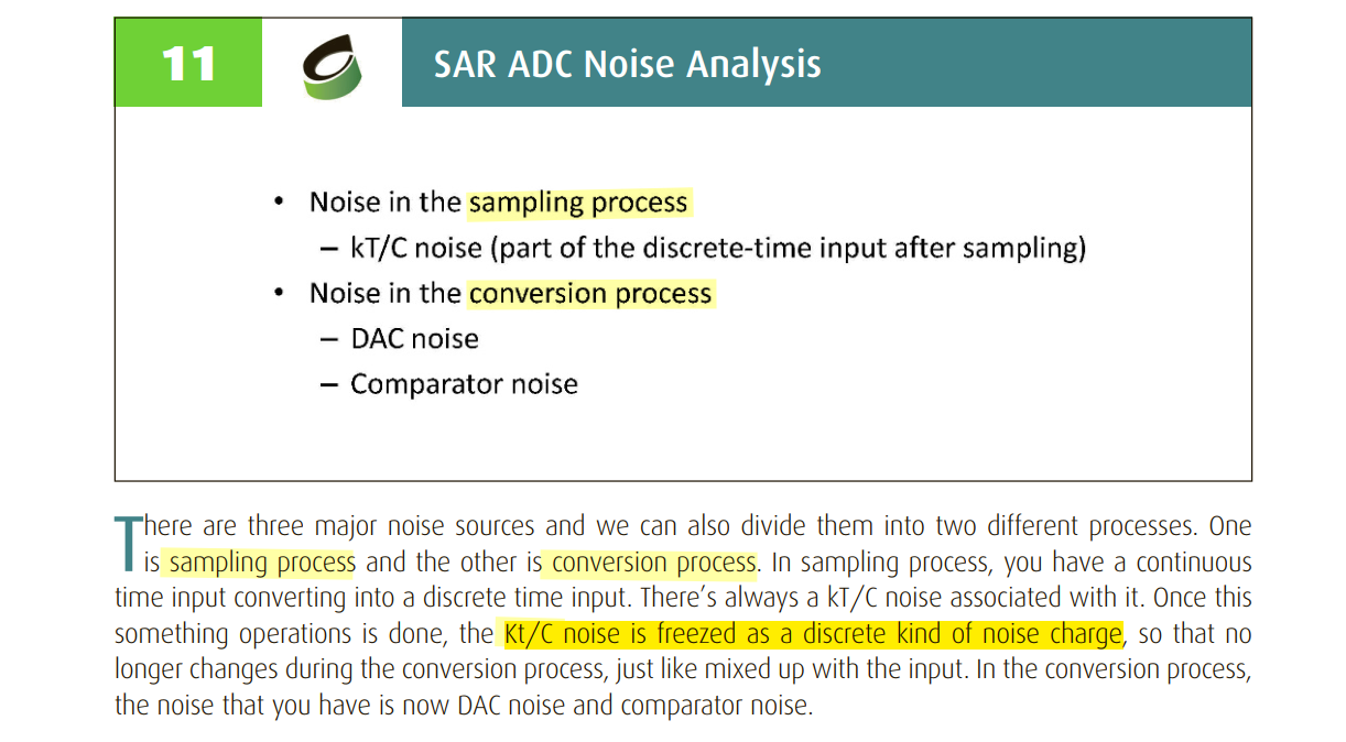
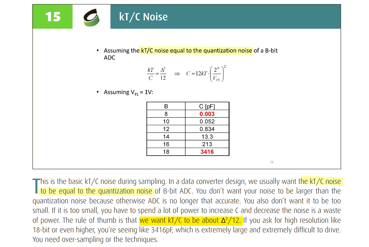
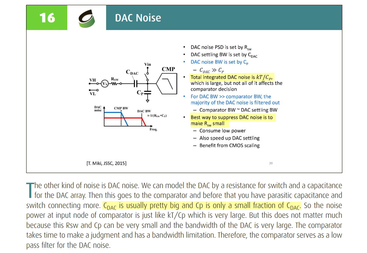
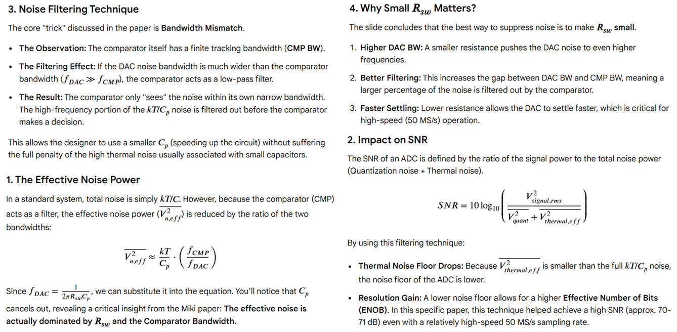
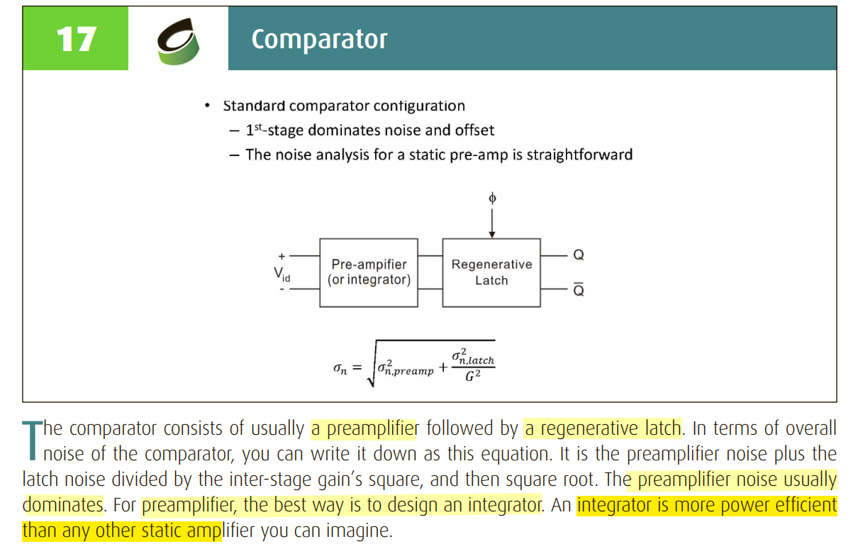
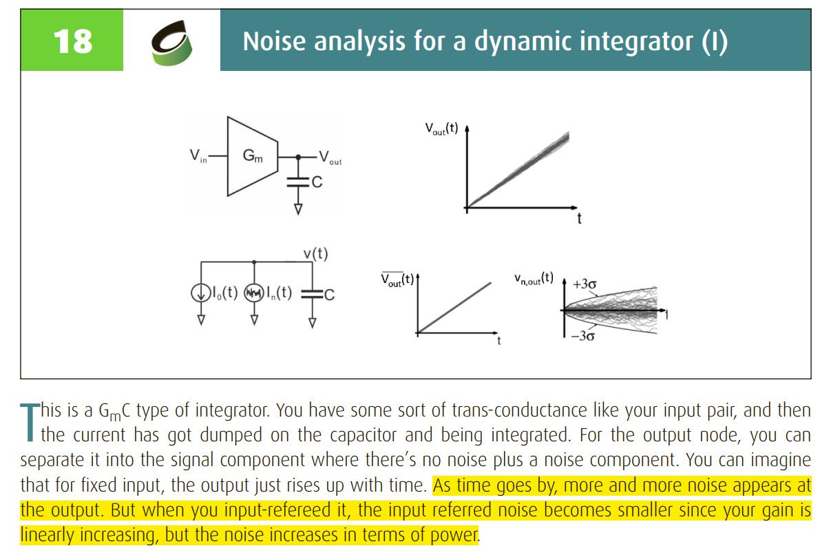
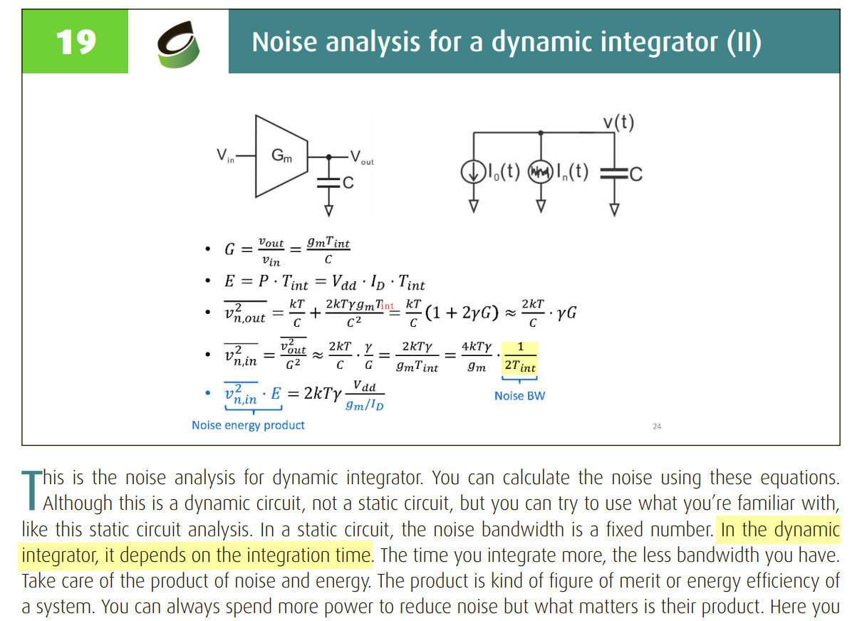
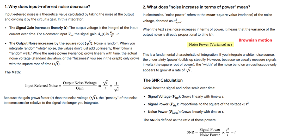
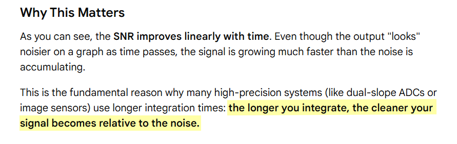
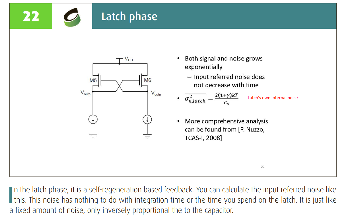
 \[
(\Delta V_i - \Delta V_x) C_1 = \Delta V_x \cdot C_2
\] Then \[
\Delta V_x = \frac{C_1}{C_1+C_2}\Delta V_i
\]
\[
(\Delta V_i - \Delta V_x) C_1 = \Delta V_x \cdot C_2
\] Then \[
\Delta V_x = \frac{C_1}{C_1+C_2}\Delta V_i
\] \[\begin{align}
V_x(s) &= \frac{C_1+C_2}{RC_1C_2}\cdot
\frac{1}{s+\frac{C_1+C_2}{RC_1C_2}}\cdot V_i(s) \\
&= \frac{1}{\tau}\cdot \frac{1}{s+\frac{1}{\tau}}\cdot \frac{1}{s}\\
&= \frac{1}{\tau}\cdot \tau(\frac{1}{s} -
\frac{1}{s+\frac{1}{\tau}})=\frac{1}{s} - \frac{1}{s+\frac{1}{\tau}}
\end{align}\]
\[\begin{align}
V_x(s) &= \frac{C_1+C_2}{RC_1C_2}\cdot
\frac{1}{s+\frac{C_1+C_2}{RC_1C_2}}\cdot V_i(s) \\
&= \frac{1}{\tau}\cdot \frac{1}{s+\frac{1}{\tau}}\cdot \frac{1}{s}\\
&= \frac{1}{\tau}\cdot \tau(\frac{1}{s} -
\frac{1}{s+\frac{1}{\tau}})=\frac{1}{s} - \frac{1}{s+\frac{1}{\tau}}
\end{align}\]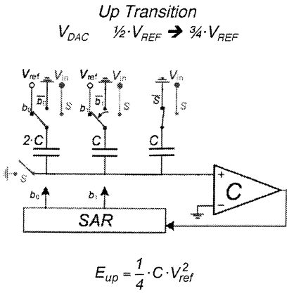
 \[
\Delta E_{tot} = \frac{1}{2}\cdot\frac{3}{4}C\cdot
V_{ref}^2 - \frac{1}{2}\cdot C\cdot V_{ref}^2 = -\frac{1}{8}CV_{ref}^2
\]
\[
\Delta E_{tot} = \frac{1}{2}\cdot\frac{3}{4}C\cdot
V_{ref}^2 - \frac{1}{2}\cdot C\cdot V_{ref}^2 = -\frac{1}{8}CV_{ref}^2
\]

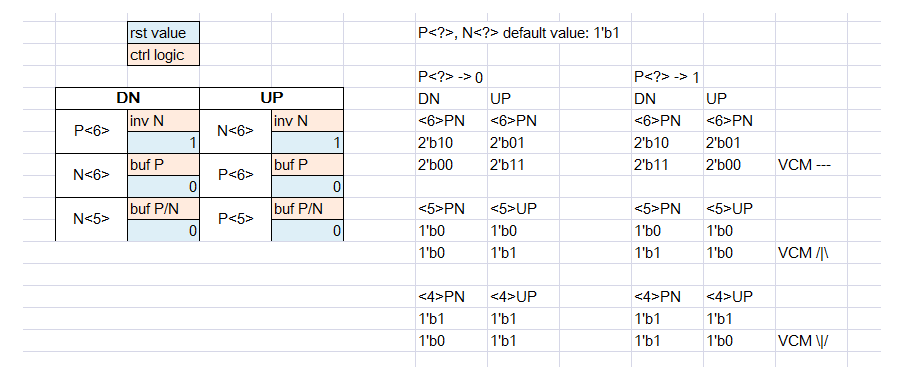
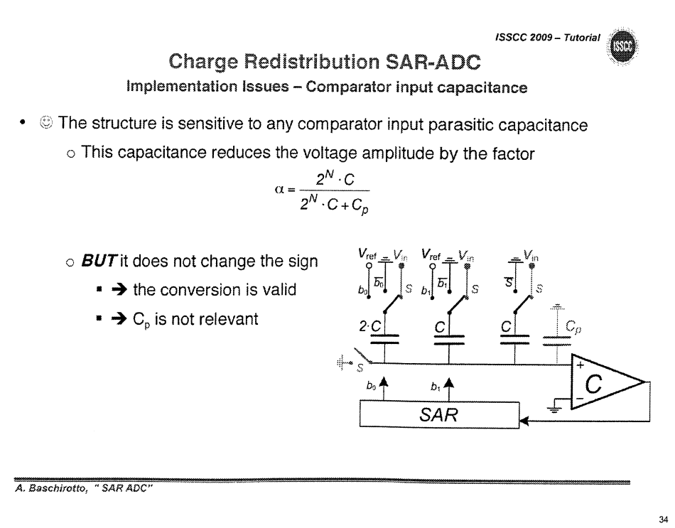 \[
-V_{in}\cdot 2^N C = V_c (2^N C + C_p)
\] Then \(V_c = -\frac{2^N C}{2^N C +
C_p}V_{in}\), i.e. this capacitance reduce the voltage amplitude
by the factor
\[
-V_{in}\cdot 2^N C = V_c (2^N C + C_p)
\] Then \(V_c = -\frac{2^N C}{2^N C +
C_p}V_{in}\), i.e. this capacitance reduce the voltage amplitude
by the factor