RLGC can be extracted from measurements of a
transmission line's input impedance under open-circuit
and short-circuit terminations at a specific
frequency
# input data, must be 2-port S2P data sub = rf.Network(args.s2p, z0=args.z0_ohm)
# physical length must be supplied by user length = args.l_um*1e-6
# target frequency for pi model extraction f_target = args.f_ghz*1e9
assert f_target < freq.stop
# get index for exctraction f = freq.f ftarget_index = rf.find_nearest_index(freq.f, f_target) omega = 2*np.pi*f[ftarget_index]
z11=sub.z[0::,0,0] # z11, the open impedance y11=sub.y[0::,0,0] # 1/y11, the short impedance Zline = np.sqrt(z11/y11) # characteristic impedance of the line
R = (gamma_ftarget*Zline_ftarget).real L = (gamma_ftarget*Zline_ftarget).imag / omega G = (gamma_ftarget/Zline_ftarget).real C = (gamma_ftarget/Zline_ftarget).imag / omega
Raymond Y. Chen, Raymond Y. Chen. Fundamentals of S Fundamentals of
S-Parameter Parameter Modeling for Power Distribution Modeling for Power
Distribution System (PDS) and SSO Analysis System (PDS) and SSO Analysis
[https://ibis.org/summits/jun05/chen.pdf]
J. H. Mikkelsen, O. K. Jensen and T. Larsen, "Crosstalk coupling
effects of CMOS co-planar spiral inductors," Proceedings of the IEEE
2004 Custom Integrated Circuits Conference [https://sci-hub.jp/10.1109/CICC.2004.1358825]
P. Guan et al., "8-Shaped Inductors: An Essential Addition to RFIC
Designers' Toolbox," in IEEE Open Journal of the Solid-State Circuits
Society, vol. 4, pp. 131-146, 2024 [pdf]
Field picture
Partial-inductance picture
Transformer
Quantity
Symbol
Meaning
Formula
Magnetic flux
\(\Phi\)
Magnetic field \(\mathbf{B}\)
passing through area \(\mathbf{S}\)
\(\Phi = \int_S \mathbf{B}\cdot
d\mathbf{S}\)
Flux linkage
\(\lambda\)
Flux linked with coil turns\(N\)
\(\lambda = N\Phi\)
Induced EMF
\(\mathcal{E}\)
Voltage generated by changing flux linkage
\(\mathcal{E} =
-\mathrm{d}\lambda/\mathrm{d}t\)
Self-inductance
\(L\)
Flux linkage caused by own current
\(L = \lambda/i\)
Mutual inductance
\(M\)
Flux linkage caused by another coil's current
\(M = \lambda_{21}/i_1\)
Coupling coefficient
\(k\)
Magnetic coupling strength between inductors
\(k = M/\sqrt{L_1L_2}\)
ideal transformer
For an ideal N:1 transformer, \[
\boxed{V_1 = N V_2} \qquad \boxed{I_1 = -\frac{I_2}{N}}
\] The minus sign comes from power conservation\[
V_1 I_1 + V_2 I_2 = 0
\] so \[
N V_2 I_1 + V_2 I_2 = 0
\] therefore \[
I_1 = -\frac{I_2}{N}
\]
So Fig. 2.3 has exactly the same two-port equations as the original
coupled inductors
Electromotive Force (EMF)
\(\mathcal{E}\)
back emf
mutual inductance
\[
M_{12}=M_{21}=M \qquad \frac{N_1\Phi_{12}}{i_2}=\frac{N_2\Phi_{21}}{i_1}
=
M
\]
Important: this does not mean\[
\Phi_{12} = \Phi_{21}
\]
\(k\) vs. \(M\)
Coupling coefficient \(k\) is based on flux
linkage ratios, not directly magnetic flux ratios
Bogatin, E. (2018). Signal and power integrity, simplified.
Prentice Hall. [pdf]
Paul, Clayton R. Inductance: Loop and Partial. Hoboken, N.J.
: [Piscataway, N.J.]: Wiley ; IEEE, 2010. [pdf]
Spartaco Caniggia. Signal Integrity and Radiated Emission of
High‐Speed Digital Systems. Wiley 2008
Luong, H. C., & Yin, J. (2016). Transformer-based design
techniques for oscillators and frequency dividers. Springer
International Publishing
ISSCC2002. Special Topic Evening Discussion Sessions SE1: Inductance:
Implications and Solutions for High-Speed Digital Circuits [vSE1_Blaauw],
[vSE1_Gauthier],
[vSE1_Morton,
[vSE1_Restle]]
Y. Massoud and Y. Ismail, "Gasping the impact of on-chip inductance,"
in IEEE Circuits and Devices Magazine, vol. 17, no. 4, pp. 14-21, July
2001 [https://sci-hub.se/10.1109/101.950046]
magnetic field (magnetic flux density, \(B\)), is the tesla
(symbol: \(T\)), defined as one
weber per square meter (\(Wb/m^2\))
Magnetic flux \(\Phi_B\) measures
the total magnetic field (\(B\))
passing through a given surface area (\(A\)), representing the number of field
lines penetrating that area. Measured in Webers (\(Wb\)),
Vector Calculus
3Blue1Brown, Divergence and curl: The language of Maxwell's
equations, fluid flow, and more [https://youtu.be/rB83DpBJQsE]
Electric Fields in Matter &
Magnetic Fields in Matter
TODO 📅
Electric Fields
Electric
field intensity \(\mathbf E\) &
Electric flux density \(\mathbf
D\)
\[
\boxed{
\underbrace{\varepsilon_0\mathbf E}_{\text{contains free + bound charge
effects}}
+
\underbrace{\mathbf P}_{\text{cancels bound-charge divergence}}
=
\underbrace{\mathbf D}_{\text{free-charge Gauss law}}
}.
\] Start from Gauss’s law for the actual electric field: \[
\nabla\cdot(\varepsilon_0\mathbf E)
=
\rho_{\text{free}}+\rho_{\text{bound}}.
\] Polarization satisfies \[
\rho_{\text{bound}}=-\nabla\cdot\mathbf P.
\] Therefore, \[
\nabla\cdot(\varepsilon_0\mathbf E)
=
\rho_{\text{free}}-\nabla\cdot\mathbf P.
\] Move the polarization term to the left: \[
\nabla\cdot(\varepsilon_0\mathbf E+\mathbf P)
=
\rho_{\text{free}}.
\] Define \[
\mathbf D=\varepsilon_0\mathbf E+\mathbf P.
\]
Electric field intensity \(\mathbf E\)
Gauss's law for \(\mathbf E\) is
\[
\boxed{
\nabla\cdot\mathbf E
=
\frac{\rho_{\text{total}}}{\varepsilon_0}
}
\] where \[
\rho_{\text{total}}
=
\rho_{\text{free}}+\rho_{\text{bound}}.
\] Therefore, \(\mathbf E\) is
determined by all charges:
externally supplied free charges,
polarization-induced bound charges.
In integral form, \[
\oint_S \mathbf E\cdot d\mathbf S
=
\frac{Q_{\text{total,enclosed}}}{\varepsilon_0}.
\]
Electric flux density \(\mathbf
D\)
Gauss's law for \(\mathbf D\) is
\[
\boxed{
\nabla\cdot\mathbf D=\rho_{\text{free}}
}
\] or \[
\boxed{
\oint_S\mathbf D\cdot d\mathbf S
=
Q_{\text{free,enclosed}}
}
\] Thus, \(\mathbf D\) is
constructed so that dielectric bound charge is absorbed into the
constitutive relation \[
\mathbf D=\varepsilon_0\mathbf E+\mathbf P.
\] It therefore relates directly only to free charge
Gauss's law for
\(\mathbf{E}\) & Gauss's law for
\(\mathbf{D}\)
\[
\boxed{
\begin{aligned}
\nabla\cdot\mathbf E
&=\frac{\rho_{\text{total}}}{\varepsilon_0},
\\[4pt]
\nabla\cdot\mathbf D
&=\rho_{\text{free}}.
\end{aligned}
}
\]
So when a textbook writes \[
\oint_S\mathbf D\cdot d\mathbf S
=
\int_V\rho_v\,dV,
\] the symbol \(\rho_v\)
normally means \[
\boxed{\rho_v=\rho_{v,\text{free}}}.
\] But when it writes \[
\oint_S\mathbf E\cdot d\mathbf S
=
\frac{1}{\varepsilon_0}\int_V\rho_v\,dV,
\] then \(\rho_v\) means the
total volume-charge density, unless the context
explicitly assumes vacuum or no polarization
Magnetostatics
Magnetostatics is the study of magnetic
fields in systems where the currents are steady (not
changing with time)
Relationship between
\(\mathbf B\) and \(\mathbf H\)
The central distinction is \[
\boxed{
\mathbf H\text{ tracks the free-current excitation, while }
\mathbf B\text{ is the resulting total magnetic flux density.}
}
\]
The general macroscopic relation is \[
\boxed{
\mathbf B=\mu_0\left(\mathbf H+\mathbf M\right)
}
\] where
\(\mathbf M\) is the magnetization
density of the material,
\(\mu_0\mathbf H\) represents the
part separated from material magnetization,
\(\mu_0\mathbf M\) is the
contribution caused by magnetic dipoles inside the material.
Therefore, \[
\boxed{
\mathbf H=\frac{\mathbf B}{\mu_0}-\mathbf M
}.
\] In vacuum
There is no material magnetization: \[
\mathbf M=0.
\] Hence, \[
\boxed{\mathbf B=\mu_0\mathbf H}.
\] In a linear, isotropic material
If \[
\mathbf M=\chi_m\mathbf H,
\] then \[
\mathbf B
=
\mu_0(1+\chi_m)\mathbf H.
\] Define \[
\mu_r=1+\chi_m,
\qquad
\mu=\mu_0\mu_r.
\] Then \[
\boxed{\mathbf B=\mu\mathbf H}.
\]
Suppose a coil carries a free current \(I\).
The free current produces an \(\mathbf
H\) field. If a magnetic material is placed inside the coil, the
material becomes magnetized: \[
I_{\mathrm{free}}
\longrightarrow
\mathbf H
\longrightarrow
\mathbf M.
\] The resulting total magnetic flux density is \[
\mathbf B=\mu_0(\mathbf H+\mathbf M).
\] Therefore: \[
\boxed{
\mathbf H
\text{ is related to the applied free current}
}
\] while \[
\boxed{
\mathbf B
\text{ includes both the applied field and the material response}.
}
\] For the same coil current, \(\mathbf
H\) may remain approximately the same, but inserting a
high-permeability core can greatly increase \(\mathbf B\).
Magnetic field intensity
\(\mathbf H\)
It is introduced to describe magnetic fields in matter while
separating the material’s magnetization from externally supplied, or
free, currents.
The Maxwell–Ampère law is \[
\boxed{
\nabla\times\mathbf H
=
\mathbf J_{\mathrm{free}}
+
\frac{\partial\mathbf D}{\partial t}
}
\] or, in integral form, \[
\boxed{
\oint_C\mathbf H\cdot d\mathbf l
=
I_{\mathrm{free}}
+
\int_S\frac{\partial\mathbf D}{\partial t}\cdot d\mathbf S
}.
\] Thus, the circulation of \(\mathbf
H\) is associated with free current.
Magnetic Flux Density \(\mathbf B\)
\(\mathbf B\) determines the
magnetic force on a moving charge.
It also defines magnetic flux: \[
\boxed{\Phi_B=\int_S\mathbf B\cdot d\mathbf S}
\] and appears in Faraday's law: \[
\oint_C\mathbf E\cdot d\mathbf l
=
-\frac{d}{dt}
\int_S\mathbf B\cdot d\mathbf S.
\] Gauss's law for magnetism is \[
\boxed{\nabla\cdot\mathbf B=0}
\] or \[
\boxed{\oint_S\mathbf B\cdot d\mathbf S=0}.
\] This is universally valid because magnetic monopoles have not
been observed.
If \[
\mathbf B=\mu\mathbf H,
\qquad
\mathbf D=\varepsilon\mathbf E,
\] with constant \(\mu\) and
\(\varepsilon\), then \[
\boxed{
\oint_C\mathbf B\cdot d\mathbf l
=
\mu I_{\mathrm{free}}
+
\mu\varepsilon
\int_S
\frac{\partial\mathbf E}{\partial t}\cdot d\mathbf S
}
\]
Gauss’s law for magnetism
The universally valid equation is \[
\boxed{\oint_S \mathbf B\cdot d\mathbf S=0}
\] or \[
\nabla\cdot\mathbf B=0.
\] This expresses that magnetic field lines have no beginning or
end—there are no observed magnetic monopoles
\[
\boxed{
\oint_S\mathbf B\cdot d\mathbf S=0
\text{ always, while }
\oint_S\mathbf H\cdot d\mathbf S=0
\text{ only under additional conditions.}
}
\] i.e. \(\mathbf B=\mu\mathbf
H\)
A. Sheikholeslami, "Current Without Electrons [Circuit Intuitions],"
in IEEE Solid-State Circuits Magazine, vol. 17, no. 4, pp. 8-10, Fall
2025
—, "Current Without Electric Field [Circuit Intuitions]," in IEEE
Solid-State Circuits Magazine, vol. 18, no. 1, pp. 8-12, winter
2026
energy and information are carried by electric and magnetic fields
(\(E\) and \(H\)) rather than by electron drift
proximity effect & skin
effect
Skin effect concentrates current near the
surface of a single conductor, while
proximity effect concentrates current in specific
regions of multiple conductors due to their
interaction
Skin effect is caused by the conductor's
own magnetic field, while proximity effect is
caused by the magnetic field of a nearby
conductor
proximity effect is a redistribution of
electric current occurring in nearby parallel
electrical conductors carrying alternating current
(AC), caused by magnetic effects (eddy
currents)
skin effect is the tendency of
AC current flow near the surface (or "skin")
of a conductor, rather than throughout its cross-section, due to the
magnetic field generated by the current
itself
Cause of skin effect
A main current \(I\) flowing through
a conductor induces a magnetic field \(H\). If the current increases, as in this
figure, the resulting increase in \(H\)
induces separate, circulating eddy currents\(I_W\) which partially cancel the
current flow in the center and reinforce it near the skin
Eddy current
By Lenz's
law, an eddy current creates a magnetic field that
opposes the change in the magnetic field that
created it, and thus eddy currents react back
on the source of the magnetic field
reference
Griffiths, David J. Introduction to Electrodynamics. Fifth
edition. Cambridge University Press, 2024. [pdf]
David Smith, Electromagnetic Theory for Complete Idiot, 2021
import numpy as np import matplotlib.pyplot as plt from scipy import signal
# Parameters: 4th order filter with 1kHz cutoff order = 4 w_cutoff = 2 * np.pi * 1000 w = np.logspace(2, 5, 1000) # Frequency range from 100Hz to 100kHz
# Generate Butterworth coefficients and frequency response b_but, a_but = signal.butter(order, w_cutoff, analog=True) w_but, h_but = signal.freqs(b_but, a_but, worN=w)
% Parameters wc = 100; % Cutoff frequency in rad/s orders = [1, 2, 6]; % Orders to compare w = logspace(0, 3, 1000); % Frequency range (1 to 1000 rad/s)
for n = orders % 1. Design Analog Filter (the 's' flag is critical) [b, a] = butter(n, wc, 's'); % 2. Calculate Complex Frequency Response h = freqs(b, a, w); % 3. Calculate Group Delay % For analog filters, we manually differentiate phase: gd = -d(phi)/dw phase = unwrap(angle(h)); gd = -diff(phase) ./ diff(w); % --- Plot Magnitude (dB) --- subplot(3,1,1); semilogx(w, 20*log10(abs(h)), 'LineWidth', 2, 'DisplayName', ['n=' num2str(n)]); hold on; % --- Plot Phase (Degrees) --- subplot(3,1,2); semilogx(w, phase * 180/pi, 'LineWidth', 2); hold on; % --- Plot Group Delay --- subplot(3,1,3); semilogx(w(1:end-1), gd, 'LineWidth', 2); hold on; end
Bessel filter is often called Bessel–Thomson
filter or simply Thomson filter
besself: Bessel analog filter design
[b,a] = besself(n, Wo)
the transfer function coefficients of an \(n\)th-order lowpass analog Bessel filter,
where Wo is the angular frequency up to which the filter's
group delay is approximately constant. Larger values of n
produce a group delay that better approximates a constant up to
Wo.
x(t) ──┬── R ──┬── y(t) │ │ │ C │ │ └───────┴── gnd
Three discretizations of the same continuous prototype, all valid
first-order LPFs but with different sample-domain behavior \(\alpha = \frac{T}{T+\tau}\):
Form
Difference equation
Transfer function
Notes
Backward Euler (above)
\(y_n = (1-\alpha) y_{n-1} + \alpha\,
x_n\)
\(\dfrac{\alpha}{1 - (1-\alpha)
z^{-1}}\)
Implicit; needs \(x_n\) before
computing \(y_n\)
Delayed leaky integrator
\(y_n = (1-\alpha) y_{n-1} + \alpha\,
x_{n-1}\)
\(\dfrac{\alpha z^{-1}}{1 - (1-\alpha)
z^{-1}}\)
One extra sample of delay; same magnitude response
Pole magnitude \(|1-\alpha| < 1\)
always — backward Euler is unconditionally stable,
unlike forward Euler (\(\alpha =
T/\tau\)), which goes unstable when \(T
> 2\tau\)
All four collapse to the same continuous-time filter as \(T \to 0\), but they're not interchangeable
at finite \(T\) — the delayed leaky
integrator in particular adds one sample of group delay that the others
don't.
Boris Murmann. EE315A VLSI Signal Conditioning Circuits
Bill Redman-White, ISSCC 2009 Tutorial: T1 : Continuous-Time
Filters
B. Nikolic, "Tutorial: Filtering in RF Transceivers," 2014 IEEE
International Solid-State Circuits Conference Digest of Technical Papers
(ISSCC), San Francisco, CA, USA, 2014
W. Sansen, "Short Course: Power Limits for Amplifiers and Filters,"
2012 IEEE International Solid-State Circuits Conference, San
Francisco, CA, USA, 2012
Antonio Liscidini, 2018 New Trends in Analog Filters
M. Babaie, "Tutorial: Role of Current-Mode Passive Mixers and N-Path
Filters in RF Receivers," 2023 IEEE International Solid-State
Circuits Conference (ISSCC), San Francisco, CA, USA, 2023
Given \(\color{red}T_p = T_s\)\[
H_\mathrm{SH}(f) \approx
\mathrm{sinc}\left( \frac{f}{f_s} \right)e^{-j\pi f T_s}
\]
\[
h_{ZOH}(t) = \text{rect}(\frac{t}{T} - \frac{1}{2}) = \left\{
\begin{array}{cl}
1 & : \ 0 \leq t \lt T \\
0 & : \ \text{otherwise}
\end{array} \right.
\] The effective frequency response is the continuous Fourier
transform of the impulse response \[
H_{ZOH}(f) = \mathcal{F}\{h_{ZOH}(t)\} = T\frac{1-e^{j2\pi fT}}{j2\pi
fT}=Te^{-j\pi fT}\text{sinc}(fT)
\] where \(\text{sinc}(x)\) is
the normalized sinc function \(\frac{\sin(\pi
x)}{\pi x}\)
The Laplace transform transfer function of the ZOH is found by
substituting \(s=j2\pi f\)\[
H_{ZOH}(s) = \mathcal{L}\{h_{ZOH}(t)\}=\frac{1-e^{-sT}}{s}
\]
Sinc Droop of ZOH sampler
Time-Domain Argument
Frequency-Domain Argument
Switched-Capacitor Filter
Kwantae Kim, Integrated Analog Systems D - Lecture 08
(Switched-Capacitor Filter) [https://youtu.be/G0lzrMll-Ho]
Due to not taking loading \(C_2\)
into account, actual switched-capacitor filter deviate from equivalent
\(R_{SC}\) + \(C_2\) low pass filter as \(f_p\) approaching to \(f_s\)
A. Abo et al., "A 1.5-V, 10-bit, 14.3-MS/s CMOS Pipeline Analog-to
Digital Converter," IEEE J. Solid-State Circuits, pp. 599, May 1999 [https://sci-hub.se/10.1109/4.760369]
Dessouky and Kaiser, "Input switch configuration suitable for
rail-to-rail operation of switched opamp circuits," Electronics Letters,
Jan. 1999. [https://sci-hub.se/10.1049/EL:19990028]
P. Schvan et al., "A 24GS/s 6b ADC in 90nm CMOS," 2008 IEEE
International Solid-State Circuits Conference - Digest of Technical
Papers, San Francisco, CA, USA, 2008, pp. 544-634
B. Sedighi, A. T. Huynh and E. Skafidas, "A CMOS track-and-hold
circuit with beyond 30 GHz input bandwidth," 2012 19th IEEE
International Conference on Electronics, Circuits, and Systems (ICECS
2012), Seville, Spain, 2012, pp. 113-116
defget_third_harmonic_bin(i, ndft): """ Finds the 3rd harmonic bin for a real-valued signal. i: fundamental bin index nfft: total number of FFT points """ # Step 1: Wrap around the sampling frequency wrapped_bin = (3 * i) % ndft ### trim N # Step 2: Fold back if it's above Nyquist if wrapped_bin > ndft // 2: harmonic_bin = ndft - wrapped_bin ### fold back to fs/2 else: harmonic_bin = wrapped_bin returnint(harmonic_bin)
defcompute_spectra(bins, v, ndft): sfdr = np.zeros(len(bins)) hd3 = np.zeros(len(bins)) spec_dbv_out = np.zeros((len(bins), ndft//2+1)) for i in bins: y = v[i-1, :] y = y[:-1] ### Coherence sanity check ### With coherent sampling, y[-1] and y[-1-ndft] should be (nearly) equal relative_error = (y[-1]-y[-1-ndft])/y[-1] print(relative_error) y = y[-ndft:] spec = np.fft.rfft(y) spec_dbv = 20*np.log10(np.abs(spec)/(ndft/2)) spec_dbv_out[i-1, :] = spec_dbv sfdr[i-1] = spec_dbv[i] - np.max(np.delete(spec_dbv, [0, i])) hd3[i-1] = spec_dbv[i] - spec_dbv[get_third_harmonic_bin(i, ndft)] return sfdr, hd3, spec_dbv_out
\(E\): oscillator-generated
component after being influenced by \(E_1\).
\(E_g\): total signal resulting
from the oscillator-generated and injected contributions.
\(\alpha(t)\) is the phase
difference between the internal oscillator phasor \(E\), after being influenced by \(E_1\), and the injected phasor \(E_1\)
\(\phi(t)\) is the angle between
that internal oscillator phasor \(E\)
and the resultant phasor \(E_g=E+E_1\)
Although \(E\) is called the
"internally generated signal," it is not the free-running, unaffected
signal. The coupling is implicit: \[
E_1
\rightarrow
E_g=E+E_1
\rightarrow
H(j\omega)
\rightarrow
E.
\] Therefore, \[
\boxed{E\text{ depends dynamically on }E_1.}
\]
Adler's Equation
\[
\boxed{\frac{\mathrm{d}\alpha}{\mathrm{d}t}
=
\Delta\omega_0
-
\frac{E_1}{E}\frac{\omega_0}{2Q}\sin\alpha}
\] Define the injection-locking strength as \[
K
=
\frac{E_1}{E}\frac{\omega_0}{2Q}.
\] Then Eq. (3) becomes the standard Adler form \[
\boxed{
\frac{\mathrm{d}\alpha}{\mathrm{d}t}
=
\Delta\omega_0-K\sin\alpha
}
\]
In steady state\[
\frac{\mathrm{d}\alpha}{\mathrm{d}t} = 0
\]
When free-running frequency is equal to injected frequency, in a
steady state, the large oscillation aligns in phase
with the small injected current
KCL plus the inductor law \[
C\dot v + \frac{v}{R} + i_L = \frac{\pi}{4}I_1\,\mathrm{sgn}(v) +
\epsilon I_1\sin(\omega_{inj}t),\qquad L\,\dot i_L = v,
\] with \(I_1\equiv\tfrac{2}{\pi}I_0\)
"inject at \(\omega_0\)" must mean
the measured free-running frequency — we measure it from an
\(\epsilon=0\) run first
phase estimates the instantaneous phase of waveform
v relative to the reference \(\sin(\omega_{\rm ref}t)\)
It acts like a simple lock-in detector:
1
N = int(round(2*np.pi / wref / dt))
Computes the number of samples in one reference period.
1 2
Ic = moving_average(2*v*sin(wref*t)) Qc = moving_average(2*v*cos(wref*t))
The one-period moving average extracts the components of
v aligned with the reference sine and cosine while
suppressing harmonics.
For
\[
v(t)=A\sin(\omega_{\rm ref}t+\phi)
\]
the averages are approximately
\[
I_c=A\cos\phi,\qquad Q_c=A\sin\phi
\]
so:
1
np.arctan2(Qc, Ic)
returns \(\phi\), in radians between
\(-\pi\) and \(\pi\)
""" Neat two-level ODE check of the slide (Dw0 = 0), one eps, one figure (3 panels). Level 1 (phase ODE, eq.3): da/dt = -B sin(a), B = (E1/E) * w0/(2Q) Level 2 (raw circuit ODE): C dv/dt + v/R + iL = Ip*sgn(v) + eps*I1*sin(w_osc*t) L diL/dt = v Both start at a0 = 90 deg (v0 ~ cos, injection ~ sin) and are compared with the slide's closed form tan(a/2) = exp(-Bt)*tan(a0/2) and with a0*exp(-Bt). Two waveform panels show v0(t) right after injection turns on (90 deg ahead of i_n) and in steady state ((1+eps)*I1*R*sin, in phase with i_n). """ import numpy as np from scipy.integrate import solve_ivp import matplotlib.pyplot as plt
# ---- parameters ------------------------------------------------------------ w0 = 2*np.pi # 1/sqrt(LC) (period = 1 s) Q, R = 10.0, 1.0 C, L = Q/(w0*R), R/(w0*Q) I1 = 1.0# limiter fundamental (= (2/pi)*I0) Ip = np.pi/4 * I1 # square-wave amplitude -> fundamental I1 eps = 0.10# E1/E B = eps*w0/(2*Q) # slide's B a0 = np.pi/2 dt, T = 2e-3, 200.0
# ---- Level 2: full circuit ODE, no averaging ------------------------------- defcircuit(t, y, eps, winj): v, iL = y dv = (Ip*np.tanh(v/0.01) + eps*I1*np.sin(winj*t) - v/R - iL)/C return dv, v/L
defphase(t, v, wref): # phase of v relative to sin(wref*t) N = int(round(2*np.pi/wref/dt)); box = np.ones(N)/N Ic = np.convolve(2*v*np.sin(wref*t), box, "same") Qc = np.convolve(2*v*np.cos(wref*t), box, "same") return np.arctan2(Qc, Ic), N
# limiter harmonics shift the autonomous frequency slightly below 1/sqrt(LC) # (Groszkowski), so measure w_osc once and inject there ("w0" of the slide): t, v = run(0.0, w0, 150.0) th, N = phase(t, v, w0) tt, thh = t[N:-N], np.unwrap(th[N:-N]) w_osc = w0 + np.polyfit(tt[tt > 50], thh[tt > 50], 1)[0]
t, v = run(eps, w_osc, T) # injection ON at t = 0 a_ckt, N = phase(t, v, w_osc)
A conventional inverter-based ring oscillator consists of a single
loop of an odd number of inverters. While compact, easy
to design and tunable over a wide frequency range, this oscillator
suffers from several limitations.
it is not possible to increase the number of phases while
maintaining the same oscillation frequency since the frequency is
inversely proportional to the number of inverters in the loop. In other
words, the time resolution of the oscillator is limited to one inverter
delay and cannot be improved below this limit.
the number of phases that can be obtained from this oscillator is
limited to odd values. Otherwise, if an even number of
inverters is used, the circuit remains in a latched state and
does not oscillate.
To overcome the limitations of conventional ring oscillators,
multi-paths ring oscillator (MPRO) is proposed. Each phase can be driven
by two or more inverters, or multi-paths instead of having each
phase in oscillator driven by a single inverter, or single
path.
One thing that makes the MPRO design problem even more complicated is
its property of having multiple possible oscillation
modes. Without a clear understanding of what makes one of these
modes dominant, it is very likely that a designer might end-up having an
oscillator that can start-up each time in a different oscillation mode
depending on the initial state of the oscillator.
In practive, the oscillator starts first from a linear mode of
operation where all the buffers are indeed acting as linear
transconductors. All oscillation modes that have mode gains, \(a_n\), lower than the actual dc gain of the
inverter, \(a_0\), start to grow.
As the oscillation amplitude grows, the effective gain of the
inverter drops due to nonlinearity. Consequently, modes with higher
mode gain die out and only the mode that requires the minimum gain
continues to oscillate and hence is the dominant mode.
The dominant mode is dependent only on the relative sizing vector
maximum oscillation
frequency
The oscillation frequency of the dominant mode of any MPRO having any
arbitrary coupling structure and number of phases is \[
f_{n^*} = \frac {1}{2\pi}\frac {(a_0-1) \cdot \sum_{i=1}^{N}x_isin\left
( \frac {2\pi n^*(i-1)}{N} \right)}{(a_0\tau _p - \tau _o)\cdot
\sum_{i=1}^{N}-x_icos\left( \frac{2\pi n^*(i-1)}{N}+(\tau _o - \tau _p)
\right)}
\]
A linear increase in the maximum possible normalized
oscillation frequency as the number of stages increases provided
that the dc gain of the buffer sufficient to provide the required
amplification
assuming unlimited dc gain and zero mode gain margins
mode stability
A common problem in MPRO design is the stability of the dominant
oscillation mode. Mode stability refers to whether the MPRO always
oscillates at the same mode regardless of the initial conditions of the
oscillator. This problem is especially pronounced for MPROs with a large
number of phases. This is due to the existence of many modes and the
very small differences in the value of the mode gain of adjacent modes
if the MPRO is not well designed.
In general, when the mode gain difference between two modes is small,
the oscillator can operate in either one depending on initial
conditions.
coupling
configurations and simulation results
Abou-El-Sonoun, A. A. (2012). High Frequency Multiphase Clock
Generation Using Multipath Oscillators and Applications. UCLA.
ProQuest ID: AbouElSonoun_ucla_0031D_10684. Merritt ID:
ark:/13030/m57p9288. Retrieved from
https://escholarship.org/uc/item/75g8j8jt
frequency stability
A problem associated with the design of MPROs is the existence of
different possible modes of oscillation. Each of these modes is
characterized by a different frequency, phase shift and phase noise.
Linear delay-stage model
(mode gain)
mode gain is based on the linear model, independent
of process but depends on coupling structure (coupling configuration,
size ratio).
The inverting buffer modeled as a linear transconductor. The
input-output relationship of a single buffer scaled by \(h_i\) and driving the input capacitance of
a similar buffer can be expressed as \[\begin{align}
h_ig_mv_{in}(t) + h_ig_oV_{out}(t)+h_iC_g\frac {dV_{out}(t)}{dt} &=
0 \\
a_nV_{in}(t)+V_{out}(t)+\tau \frac {V_{out}(t)}{dt} &= 0
\end{align}\] where \(g_m\) is
the transconductance, \(g_o\) is the
output conductance, \(C_g\) is the
buffer input capacitance which also acts as the load capacitance for the
driving buffer, and \(a_n = \frac
{g_m}{g_o}\) is the linear dc gain of the
buffer, and \(\tau=\frac {C_g}{g_o}\)
is a time constant.
Similarly, \(V_1\), the output of
the first stage in MPRO can be expressed \[
\sum_{i=1}^{N}h_ig_mV_i(t)+\sum_{i=1}^{N}h_ig_oV_i(t)+\sum_{i=1}^{N}h_iC_g\frac
{dV_it(t)}{dt} = 0
\] Defining the fractional sizing factors and the total sizing
factor as \(x_i=\frac{h_i}{H}\) and
\(H=\sum_{i=1}^{N}h_i\)\[
a_n\sum_{i=1}^{N}x_iV_i(t) + V_1(t)+\tau\frac {dV_i(t)}{dt} = 0
\] where \(a_n = \frac
{g_m}{g_o}\) and \(\tau=\frac
{C_g}{g_o}\) are same dc gain and time constant defined
previously
Since the total phase shift around the loop should be multiples of
\(2\pi\), the oscillation waveform at
the ith node can be expressed as \[
V_i(t) = V_o \cos(\omega_nt-\Delta \varphi \cdot i)
\] where \(\omega_n\) is the
oscillation frequency and \(\Delta \varphi =
\frac {2\pi n}{N}\), \(N\) is
the number of stages in the oscillator and \(n\) can take values between \(0\) and \(N-1\)
Plug \(V_i(t)\) into differential
equation, we get \[
a_n\sum_{i=1}^{N}x_i\cos(\omega_n t-\frac{2\pi n}{N}i)+\cos(\omega_n
t-\frac{2\pi n}{N}) - \omega_n \tau \sin(\omega_n t-\frac{2\pi n}{N}) =
0
\] By equating the \(cos(\omega_n
t)\) and \(sin(\omega_n t)\)
terms of the above equation, we get expressions for the
oscillation frequency of the nth mode and the
minimum dc gain required for this mode to exist. we refer to
this gain as the mode gain\[\begin{align}
\omega_n\tau &= \frac {\sum_{i=1}^{N}x_i \cdot \sin(\frac{2\pi
n}{N}(i-1))}{-\sum_{i=1}^{N}x_i \cdot \cos(\frac{2\pi n}{N}(i-1))} \\
a_n &= \frac {1}{-\sum_{i=1}^{N}x_i \cdot \cos(\frac{2\pi
n}{N}(i-1))}
\end{align}\] where \(a_n\)
should be greater than \(0\) for a
existent mode
In practice, the oscillator starts first from a linear mode of
operation where all the buffers are indeed acting as linear
transconductors. All oscillation modes that have mode gains \(a_n\) lower than the actual dc gain of the
inverter \(a_o\) start to grow. As the
oscillation amplitude grows, the effective gain of the inverter drops
due to nonlinearity. Consequently, modes with higher mode gain die
out and only the mode that requires the minimum gain continues to
oscillate and hence is the dominant mode
A. A. Hafez and C. K. Yang, "Design and Optimization of Multipath
Ring Oscillators," in IEEE Transactions on Circuits and Systems I:
Regular Papers, vol. 58, no. 10, pp. 2332-2345, Oct. 2011, doi:
10.1109/TCSI.2011.2142810.
Simulation-based approach
GCHECK is an automated verification tool that
validate whether a ring oscillator always converges to the desired mode
of operation regardless of the initial conditions and
variability conditions. This is the first tool ever
reported to address the global convergence failures in presence of
variability. It has been shown that the tool can successfully validate a
number of coupled ring oscillator circuits with various global
convergence failure modes (e.g. no oscillation, false oscillation, and
even chaotic oscillation) with reasonable computational costs such as
running 1000-point Monte-Carlo simulations for 7~60 initial conditions
(maximum 4 hours).
The verification is performed using a predictive global
optimization algorithm that looks for a problematic initial
state from a discretized state space
despite the finite number of initial state
candidates considered and finite number of Monte-Carlo
samples to model variability, the proposed algorithm can verify
the oscillator to a prescribed confidence level
The observation that the responses of a circuit with nearby initial
conditions are strongly correlated with respect to common variability
conditions enables us to explore a discretized version
of the initial condition space instead of the continuous one.
the settling time increases as the initial state gets farther away
from the equilibrium state allowed us to use the settling time as a
guidance metric to find a problematic initial condition.
Selecting the Next Initial Condition Candidate to
Evaluate
To determine whether the algorithm should continue or terminate the
search for a new maximum, the algorithm estimates the probability of
finding a new initial condition with the longer settling
time, based on the information obtained with the
previously-evaluated initial conditions.
GCHECK EXAMPLE
1
python gcheck_osc.py input.scs
output log:
1 2 3 4 5 6 7 8
Step 1/4: Simulating the setting-time distribution with the reference initial condition ... Step 2/4: Simulating the setting-time distribution for randomly-selected initial probes ... Step 3/4: Searching for Problematic Initial Conditions ... Step 4/4: Reporting Verification Results and Statistics ...
T. Kim, D. -G. Song, S. Youn, J. Park, H. Park and J. Kim, "Verifying
start-up failures in coupled ring oscillators in presence of variability
using predictive global optimization," 2013 IEEE/ACM International
Conference on Computer-Aided Design (ICCAD), 2013, pp. 486-493 GCHECK:
Global Convergence Checker for
Oscillators](https://mics.snu.ac.kr/wiki/GCHECK)
Mathuranathan, Line code – demonstration in Matlab and Python [link]
For unipolar NRZ line coded signal, the average value of the
signal is not zero and hence they have a significant DC
component
The DC impulses in the PSD do not carry any information and it also
causes the transmission wires to heat up. This is a wastage of
communication resource
The bipolar NRZ signal is devoid of a significant impulse at the
zero frequency (DC component is very close to zero)
Furthermore, it has more power than the unipolar line code (note: PSD
curve for bipolar NRZ is slightly higher compared to that of unipolar
NRZ). Therefore, bipolar NRZ signals provide better signal-to-noise
ratio (SNR) at the receiver.
Both Unipolar and Bipolar NRZ signal lacks embedded clock
information, which posses synchronization problems at the receiver when
the binary information has long runs of 0s and 1s
Baseline Wander
David A. Johns, ECE1392H - Integrated Circuits for Digital
Communications - Fall 2001 [Equalization]
Then rise time of 20% to 80% is \[
T_{r} = \tau_{RC}\cdot \ln\frac{0.8}{0.2} = 1.3863 \cdot \tau_{RC}
\] we have \[
f_{3dB} = \frac{1}{2\pi}\frac{1}{\tau_{RC}} = \frac{1}{2\pi}\frac{
1.3863}{T_r} = \frac{0.22}{T_r}
\]
Since we have (ideally) no return current, the ground
reference becomes less important. The ground potential can
even be different at the sender and receiver or moving around within a
certain acceptable range. However, you need to be careful because
DC-coupled differential signaling (such as USB, RS-485, CAN) generally
requires a shared ground potential to ensure that the signals stay
within the interface's maximum and minimum allowable common-mode
voltage.
Tony Chan Carusone, Alphawave Semi. VLSI2025 SC2: Connectivity
Technologies to Accelerate AI
Jitter Performance
Limitations
Aliasing of baud-rate
sampling
The most significant impairments are considered to be the sensitivity
to sampling phase, and the effect of aliasing out of band signal and
noise into the baseband
D. S. Millar, D. Lavery, R. Maher, B. C. Thomsen, P. Bayvel and S. J.
Savory, "A baud-rate sampled coherent transceiver with digital pulse
shaping and interpolation,"in OFC 2013 [https://www.merl.com/publications/docs/TR2013-010.pdf]
Tahmoureszadeh, Tina. Master's Theses (2009 - ): Analog Front-end
Design for 2x Blind ADC-based Receivers [http://hdl.handle.net/1807/29988]
Shafik, Ayman Osama Amin Mohamed. "Equalization Architectures for
High Speed ADC-Based Serial I/O Receivers." PhD diss., 2016. [https://core.ac.uk/download/79652690.pdf]
"ISI cancellation" based equalization is conceptually more
straightforward but suffers from SNR penalty or error propagation
Jitter Amplification
by Passive Channels
Enhancing
Resolution with a \(\Delta \Sigma\)
Modulator
Sub-Resolution Time Averaging
\(\Delta \Sigma\) modulator
effectively dithers the LSB bit
between zero and one, such that you can get the effective
resolution of a much higher resolution DAC in the number of bits
Decimation
how they affect sampling phase
DLF's input bit-width can be reduced by decimating BBPD's
output. Decimation is typically performed by realizing either
majority voting (MV) or boxcar
filtering.
Note that deserialization is inherent to both
MV and boxcar filtering
Decimation is commonly employed to alleviate the high-speed
requirement. However, decimation increases loop-latency which causes
excessive dither jitter.
Decimation is basically, widen the data and slowing it down
Decimating by \(L\) means frequency
register only added once every \(L\)
UI, thus integral path gain reduced by \(L\) in linear model
proportional path gain is unchanged
CDR Linear Model
condition:
Linear model of the CDR is used in a frequency lock
condition and is approaching to achieve phase
lock
Using this model, the power spectral density (PSD) of jitter in the
recovered clock \(S_{out}(f)\) is \[
S_{out}(f)=|H_T(f)|^2S_{in}(f)+|H_G(f)|^2S_{VCO}(f)
\] Here, we assume \(\varphi_{in}\) and \(\varphi_{VCO}\) are uncorrelated as they
come from independent sources.
Using below notation \[\begin{align}
\omega_n^2=\frac{K_{PD}K_{VCO}}{C} \\
\xi=\frac{K_{PD}K_{VCO}}{2\omega_n^2}
\end{align}\]
We can rewrite transfer function as follows \[
H_T(s)=\frac{2\xi\omega_n s+\omega_n^2}{s^2+2\xi \omega_n s+\omega_n^2}
\]
The jitter transfer represents a low-pass filter
whose magnitude is around 1 (0 dB) for low jitter frequencies and drops
at 20 dB/decade for frequencies above \(\omega_n\)
the recovered clock track the low-frequency
jitter of the input data
the recovered clock DONT track the
high-frequency jitter of the input data
The recovered clock does not suffer from high-frequency jitter even
though the input signal may contain high-frequency jitter, which will
limit the CDR tolerance to high-frequency jitter.
Jitter Peaking in
Jitter Transfer Function
The peak, slightly larger than 1 (0dB) implies that jitter will be
amplified at some frequencies in the CDR, producing a
jitter amplitude in the recovered clock, and thus also in the recovered
data, that is slightly larger than the jitter amplitude
in the input data.
This is certainly undesirable, especially in applications such as
repeaters.
Jitter Generation
If the input data to the CDR is clean with no jitter, i.e., \(\varphi_{in}=0\), the jitter of the
recovered clock comes directly from the VCO jitter. The transfer
function that relates the VCO jitter to the recovered clock jitter is
known as jitter generation. \[
H_G(s)=\frac{\varphi_{out}}{\varphi_{VCO}}|_{\varphi_{in}=0}=\frac{s^2}{s^2+2\xi
\omega_n s+\omega_n^2}
\] Jitter generation is high-pass filter with
two zeros, at zero frequency, and two poles identical to those of the
jitter transfer function
Jitter Tolerance (JTOL)
To quantify jitter tolerance, we often apply a sinusoidal jitter of a
fixed frequency to the CDR input data and observe the BER of the CDR
The jitter tolerance curve DONT capture a CDR's true
tolerance to random jitter. Because we are applying
"sinusoidal" jitter, which is deterministic signal.
We can deal only with the jitter's amplitude and frequency instead of
the PSD of the jitter thanks to deterministic sinusoidal jitter signal.
\[
JTOL(f) = \left | \varphi_{in}(f) \right |_{\text{pp-max}} \quad
\text{for a fixed BER}
\] Where the subscript \(\text{pp-max}\) indicates the
maximum peak-to-peak amplitude. We can further expand
this equation as follows \[
JTOL(f)=\left| \frac{\varphi_{in}(f)}{\varphi_{e}(f)} \right| \cdot
|\varphi_e(f)|_\text{pp-max}
\]
Relative jitter, \(\varphi_e\) must
be less than 1UIpp for error-free operation
In an ideal CDR, the maximum peak-to-peak amplitude
of \(|\varphi_e(f)|\) is
1UI, i.e.,\(|\varphi_e(f)|_\text{pp-max}=1UI\)
Accordingly, jitter tolerance can be expressed in terms of the number
of UIs as \[
JTOL(f)=\left| \frac{\varphi_{in}(f)}{\varphi_{e}(f)} \right|\quad
\text{[UI]}
\] Given the linear CDR model, we can write \[
JTOL(f)=\left| 1+\frac{K_{PD}K_{VCO}H_{LF}(f)}{j2\pi f} \right|\quad
\text{[UI]}
\] Expand \(H_{LF}(f)\) for the
CDR, we can write \[
JTOL(f)=\left| 1-2\xi j \left(\frac{f_n}{f}\right) -
\left(\frac{f_n}{f}\right)^2 \right|\quad \text{[UI]}
\] At frequencies far below and above the natural frequency, the
jitter tolerance can be approximated by the following \[
JTOL(f) = \left\{ \begin{array}{cl}
\left(\frac{f_n}{f}\right)^2 & : \ f\ll f_n \\
1 & : \ f\gg f_n
\end{array} \right.
\]
the jitter tolerance at very high jitter frequencies
is limited to 1UIpp
1 2 3 4 5 6 7 8 9 10 11 12 13 14
clc;
clear all;

f_fn = logspace(-1, 2, 60);
for xi = [2, 1, 0.5, 0.2]
    jtol = abs(1- 1i*2*xi.*(1./f_fn)- (1./f_fn).^2);
    loglog(f_fn, jtol,LineWidth=2)
    disp(["min(JTpp)=", min(jtol),"@\xi=",xi])
    hold on
end
grid on;
xlabel("f/f_n")
ylabel('JT_{pp}')
legend('\xi=2', '\xi=1', '\xi=0.5', '\xi=0.2')
JTF, by jitter frequency, compares how much input signal jitter is
transferred to the output of a clock-recovery's PLL (recovered
clock)
Input signal jitter that is within the clock recovery PLL's loop
bandwidth results in jitter that is faithfully transferred (closed-loop
gain) to the clock recovery PLL's output signal. JTF in this situation
is approximately 1.
Input signal jitter that is outside the clock recovery PLL's loop
bandwidth results in decreasing jitter (open-loop gain) on the clock
recovery PLL's output, because the jitter is filtered out and no longer
reaches the PLL's VCO
Observed Jitter Transfer Function
Input Signal Versus Sampled Signal
OJTF compares how much input signal jitter is transferred to the
output of a receiver's decision making circuit as
effected by a clock recovery's PLL. As the recovered clock is the
reference for detecting the input signal
Input signal jitter that is within the clock
recovery PLL's loop bandwidth results in jitter on the recovered clock
which reduces the amount of jitter that can be detected. The input
signal and clock signal are closer in phase
Input signal jitter that is outside the clock
recovery PLL's loop bandwidth results in reduced jitter on the
recovered clock which increases the amount of jitter that can
be detected. The input signal and clock signal are more out of phase.
Jitter that is on both the input and clock signals can not detected or
is reduced
JTF and OJTF for 1st Order PLLs
The observed jitter is a complement to the PLL jitter transfer
response OJTF=1-JTF (Phase matters!)
OTJF gives the amount of jitter which is tracked and therefore not
observed at the output of the CDR as a function of the jitter rate
applied to the input.
The combination of the OJTF of a jitter measurement device and the
JTF of the clock generator under test gives the measured jitter as a
function of frequency.
For example, a clock generator with a type 1, 1st order PLL measured
with a jitter measurement device employing a golden PLL is \[
J_{\text{measured}} = \frac{\omega_1}{s+\omega_1}\frac{s}{s+\omega_2}
\]
Accurate measurement of the clock JTF requires that the OJTF cutoff
of the jitter measurement be significantly below that of the clock JTF
and that the measurement is compensated for the instrument's OJTF.
The overall response is a band pass filter because the clock JTF is
low pass and the jitter measurement device OJTF is high pass.
The compensation for the instrument OJTF is performed by measuring
the jitter of the reference clock at each jitter rate being tested and
comparing the reference jitter with the jitter
measured at the output of the DUT.
The lower the cutoff frequency of the jitter measurement device the
better the accuracy of the measurement will be.
The cutoff frequency is limited by several factors including the
phase noise of the DUT and measurement time.
Digital Sampling
Oscilloscope
How to analyze jitter:
TIE (Time Interval Error) track
histogram
FFT
TIE track provides a direct view of how the phase of
the clock evolves over time.
histogram provides valuable information about the
long term variations in the timing.
FFT allows jitter at specific rates to be measured
down to the femto-second range.
Maintaining the record length at a minimum of \(1/10\) of the inverse of the PLL loop
bandwidth minimizes the response error
reference
Dalt, Nicola Da and Ali Sheikholeslami. “Understanding Jitter and
Phase Noise: A Circuits and Systems Perspective.” (2018).
quantization noise is ~ bounded uniform distribution
Using unbounded Gaussian -> pessimistic BER prediction
AFE Nonlinearity
"total harmonic distortion" (THD) in
AFE
Relative to NRZ-based systems, PAM4 transceivers require more
stringent circuit linearity, equalizers which can implement multi-level
inter-symbol interference (ISI) cancellation, and improved
sensitivity
Because if it compresses, it turns out you have to use a much more
complicated feedback filter. As long as it behaves linearly,
the feedback filter itself can remain a linear FIR
Linearity can actually be a critical constraint in these signal
paths, and you really want to stay as linear as you can all the way up
until the point where you've canceled all of the ISI
Elad Alon, ISSCC 2014, "T6: Analog Front-End Design for Gb/s Wireline
Receivers"
BER with Quantization Noise
\[
\text{Var}(X) = E[X^2] - E[X]^2
\]
Impulse Response or Pulse
Response
TX FFE
TX FFE suffers from the peak power constraint, which in effect
attenuates the average power of the outgoing signal - the low-frequency
signal content has been attenuated down to the high-frequency level
H. Shakiba, D. Tonietto and A. Sheikholeslami, "High-Speed Wireline
Links-Part II: Optimization and Performance Assessment," in IEEE Open
Journal of the Solid-State Circuits Society, vol. 4, pp. 110-121, 2024
[https://ieeexplore.ieee.org/stamp/stamp.jsp?tp=&arnumber=10579874]
R. Walker, “Designing Bang-Bang PLLs for Clock and Data Recovery in
Serial Data Transmission Systems,” in Phase-Locking in High-Performance
Systems, B. Razavi, Ed. New Jersey: IEEE Press, 2003, pp. 34-45. [http://www.omnisterra.com/walker/pdfs.papers/BBPLL.pdf]
P. K. Hanumolu, M. G. Kim, G. -y. Wei and U. -k. Moon, "A 1.6Gbps
Digital Clock and Data Recovery Circuit," IEEE Custom Integrated
Circuits Conference 2006, San Jose, CA, USA, 2006, pp. 603-606 [https://sci-hub.se/10.1109/CICC.2006.320829]
Da Dalt N. A design-oriented study of the nonlinear dynamics of
digital bang-bang PLLs. IEEE Transactions on Circuits and Systems I:
Regular Papers. 2005;52(1):21–31. [https://sci-hub.se/10.1109/TCSI.2004.840089]
Jang S, Kim S, Chu SH, Jeong GS, Kim Y, Jeong DK. An optimum loop
gain tracking all-digital PLL using autocorrelation of bang–bang phase
frequency detection. IEEE Transactions on Circuits and Systems II:
Express Briefs. 2015;62(9):836–840. [https://sci-hub.se/10.1109/TCSII.2015.2435691]
CDR Loop Latency
Denoting the CDR loop latency by \(\Delta
T\) , we note that the loop transmission is multiplied by \(exp(-s\Delta T)\simeq 1-s\Delta T\).The
resulting right-half-plane zero, \(f_z\) degrades the phase margin and must
remain about one decade beyond the BW\[
f_z\simeq \frac{1}{2\pi \Delta T}
\]
This assumption is true in practice since the bandwidth of the CDR
(few mega Hertz) is much smaller than the data rate (multi giga
bits/second).
Homayoun, Aliakbar and Behzad Razavi. “On the Stability of
Charge-Pump Phase-Locked Loops.” IEEE Transactions on Circuits and
Systems I: Regular Papers 63 (2016): 741-750.
N. Kuznetsov, A. Matveev, M. Yuldashev and R. Yuldashev, "Nonlinear
Analysis of Charge-Pump Phase-Locked Loop: The Hold-In and Pull-In
Ranges," in IEEE Transactions on Circuits and Systems I: Regular
Papers, vol. 68, no. 10, pp. 4049-4061, Oct. 2021
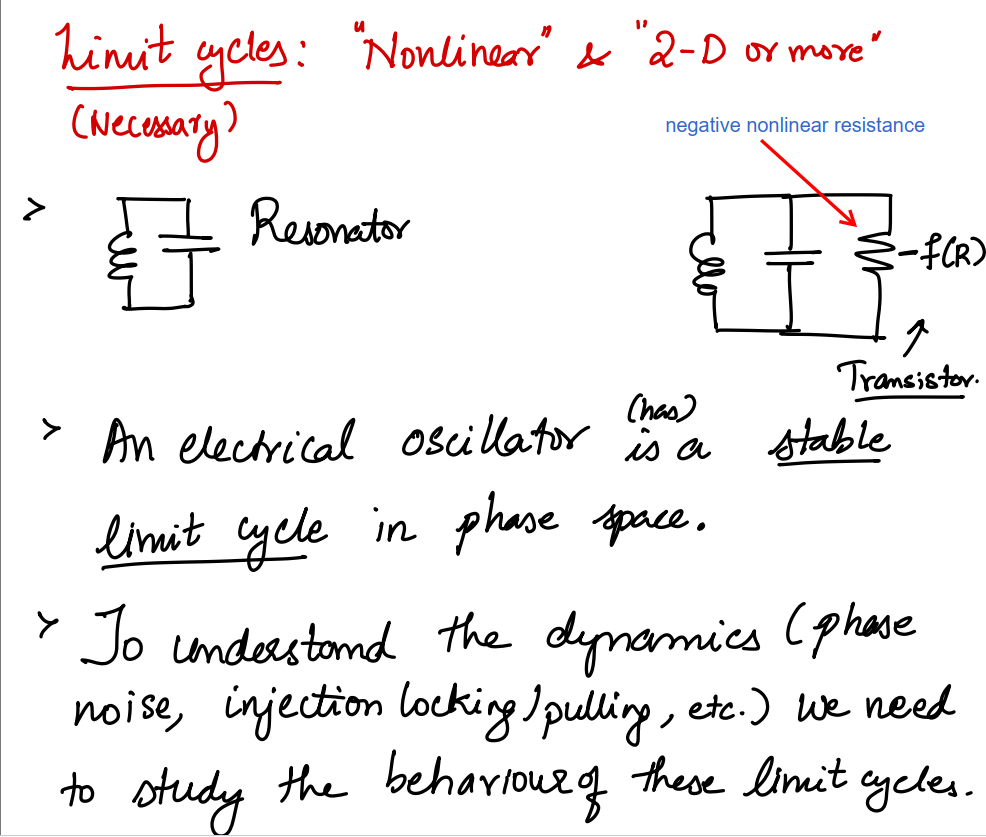
limit cycles imply self-sustained oscillators due nonlinear
nature
Ouzounov, S., Hegt, H., Van Roermund, A. (2007). SUB-HARMONIC
LIMIT-CYCLE SIGMA-DELTA MODULATION, APPLIED TO AD CONVERSION. In: Van
Roermund, A.H., Casier, H., Steyaert, M. (eds) Analog Circuit Design.
Springer, Dordrecht. [https://sci-hub.se/10.1007/1-4020-5186-7_6]
Digital CDR Category
DCO part is analogous so that it cannot be perfectly
modeled
Digital-to-phase converter is well-defined phase output, thus, very
good to model real situation
Z-domain modeling
The difference equation is \[
\phi[n] = \phi[n-1] + K_{DCO}V_C[n]\cdot T\cdot2\pi
\] z-transform is \[
\frac{\Phi(z)}{V_C(z)}=\frac{2\pi K_{DCO}T}{1-z^{-1}}
\]
where \(K_{DCO}\) : \(\Delta f\) (Hz/bit)
\(\Delta
\Sigma\)-dithering in DCO
Quantization noise
Here, \(\alpha_T\) is data
transition density
BBPD quantization noise
DAC quantization noise
M. -J. Park and J. Kim, "Pseudo-Linear Analysis of Bang-Bang
Controlled Timing Circuits," in IEEE Transactions on Circuits and
Systems I: Regular Papers, vol. 60, no. 6, pp. 1381-1394, June 2013 [https://sci-hub.st/10.1109/TCSI.2012.2220502]
Time to Digital Converter
(TDC)
Digital to Phase Converter
(DPC)
IIR low pass filter
simple approximation: \[
z = 1 + sT
\] bilinear-z transform \[
z =\frac{}{}
\]
FAQ
PLL vs. CDR
PLL
CDR
Clock edge periodic
Data edge random
Phase & Frequency detecting possible
Phase detecting possible , Frequency detecting impossible
PLL or FD(Frequency Detector) for frequency detecting in CDR
reference
J. Stonick. ISSCC 2011 "DPLL-Based Clock and Data Recovery" [slides,transcript]
P. Hanumolu. ISSCC 2015 "Clock and Data Recovery Architectures and
Circuits" [slides]
Amir Amirkhany. ISSCC 2019 "Basics of Clock and Data Recovery
Circuits"
Fulvio Spagna. INTEL, CICC2018, "Clock and Data Recovery Systems" [slides]
M. Perrott. 6.976 High Speed Communication Circuits and Systems
(lecture 21). Spring 2003. Massachusetts Institute of Technology: MIT
OpenCourseWare, [lec21.pdf]
Akihide Sai. ISSCC 2023, T5 "All Digital Plls From Fundamental
Concepts To Future Trends" [T5.pdf]
J. L. Sonntag and J. Stonick, "A Digital Clock and Data Recovery
Architecture for Multi-Gigabit/s Binary Links," in IEEE Journal of
Solid-State Circuits, vol. 41, no. 8, pp. 1867-1875, Aug. 2006 [https://sci-hub.se/10.1109/JSSC.2006.875292]
—, "A digital clock and data recovery architecture for
multi-gigabit/s binary links," Proceedings of the IEEE 2005 Custom
Integrated Circuits Conference, 2005.. [https://sci-hub.se/10.1109/CICC.2005.1568725]
P. Palestri et al., "Analytical Modeling of Jitter in
Bang-Bang CDR Circuits Featuring Phase Interpolation," in IEEE
Transactions on Very Large Scale Integration (VLSI) Systems, vol.
29, no. 7, pp. 1392-1401, July 2021 [https://sci-hub.se/10.1109/TVLSI.2021.3068450]
Rhee, W. (2020). Phase-locked frequency generation and clocking :
architectures and circuits for modern wireless and wireline
systems. The Institution of Engineering and Technology
M.H. Perrott, Y. Huang, R.T. Baird, B.W. Garlepp, D. Pastorello, E.T.
King, Q. Yu, D.B. Kasha, P. Steiner, L. Zhang, J. Hein, B. Del Signore,
"A 2.5 Gb/s Multi-Rate 0.25μm CMOS Clock and Data Recovery Circuit
Utilizing a Hybrid Analog/Digital Loop Filter and All-Digital
Referenceless Frequency Acquisition," IEEE J. Solid-State Circuits, vol.
41, Dec. 2006, pp. 2930-2944 [https://cppsim.com/Publications/JNL/perrott_jssc06.pdf]
—, et al., "Modeling of ADC-Based Serial Link Receivers With
Embedded and Digital Equalization," in IEEE Transactions on
Components, Packaging and Manufacturing Technology, vol. 9, no. 3,
pp. 536-548, March 2019 [https://sci-hub.se/10.1109/TCPMT.2018.2853080]
K. Zheng, "System-Driven Circuit Design for ADC-Based Wireline Data
Links", Ph.D. Dissertation, Stanford University, 2018 [https://purl.stanford.edu/hw458fp0168]
S. Cai, A. Shafik, S. Kiran, E. Z. Tabasy, S. Hoyos and S. Palermo,
"Statistical modeling of metastability in ADC-based serial I/O
receivers," 2014 IEEE 23rd Conference on Electrical Performance of
Electronic Packaging and Systems [pdf]
F. L. Traversa, M. Bonnin and F. Bonani, "The Complex World of
Oscillator Noise: Modern Approaches to Oscillator (Phase and Amplitude)
Noise Analysis," in IEEE Microwave Magazine, vol. 22, no. 7,
pp. 24-32, July 2021 [https://sci-hub.ru/10.1109/MMM.2021.3069535]
Phase Noise Definition
Eq. (3.25) is widely adopted by industry and academia
using the narrow angle assumption, the two definitions above
are equivalent
If the narrow angle condition is not satisfied, however, the
two definitions differ
M.H. Perrott, Short Course On Phase-Locked Loops and Their
Applications Day 2, AM Lecture Basic Building Blocks
Voltage-Controlled Oscillators [https://www.cppsim.com/PLL_Lectures/day2_am.pdf]
A. Hajimiri and T. H. Lee, "A general theory of phase noise in
electrical oscillators," in IEEE Journal of Solid-State
Circuits, vol. 33, no. 2, pp. 179-194, Feb. 1998 [paper],
[slides]
—, RFIC 2024 Technical Lecture: Noise in Oscillators from
Understanding to Design
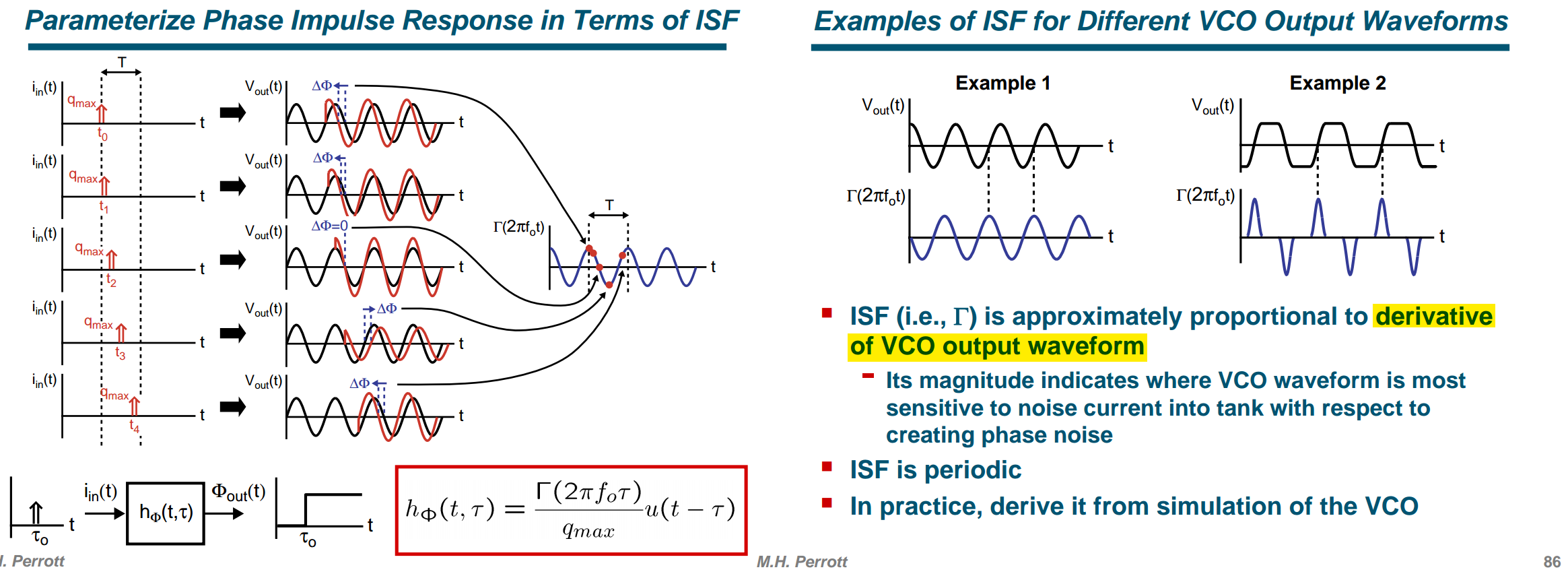
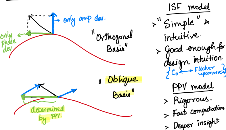
The peak magnitude of the ISF, \[
\Gamma_{\max}=\max_\theta |\Gamma(\theta)|,
\] can be greater than 1, equal to 1, or less than
1.
A value \(\Gamma>1\) therefore
does not mean "more than 100%." It simply means that
the oscillator has relatively high phase sensitivity at that particular
phase.
\(\psi(t)\) is literally the
instantaneous frequency deviation. Check the dimensions: \(i(t)/q_{max}\) has units of A/C = 1/s, and
\(\Gamma\) is dimensionless, so \(\psi(t) = \Gamma(\omega_0
t)\,i(t)/q_{max}\) is in rad/s. The diagram is saying \(d\phi/dt = \psi(t)\), i.e. \(\phi(t) =
\int_{-\infty}^{t}\psi(\tau)d\tau\). An ideal integrator has
transfer function \(1/j\Delta\omega\),
so in power spectra: \[
S_\phi(\Delta\omega) = \frac{S_\psi(\Delta\omega)}{\Delta\omega^2}
\] That single block is the origin of every\(1/\Delta\omega^2\) factor in phase noise
theory — including the \((\omega_0/2Q\Delta\omega)^2\) term in
Leeson's equation
Pure sinusoidal voltage
White-noise Folding
Suppose a low frequency sinusoidal perturbation current \(i(t) = I_m \cos[(m\omega_0 +\Delta
\omega)t]\),
If \(m=0\)\[
\phi(t) \approx \frac{I_0C_0}{2q_\text{max}\Delta
\omega}\sin(\Delta\omega t)
\] If \(m\neq 0\) and \(m=n\)\[
\phi(t) \approx \frac{I_mC_m}{2q_\text{max}\Delta
\omega}\sin(\Delta\omega t)
\]
When performing the phase noise computation
integral, there will be a negligible contribution from all
terms, other than \(n=m\)
apply equation (18) derived from sinusoidal
to white noise
Corrections to "A General Theory of Phase Noise in
Electrical Oscillators"
A. Hajimiri and T. H. Lee, "Corrections to "A General Theory of Phase
Noise in Electrical Oscillators"," in IEEE Journal of Solid-State
Circuits, vol. 33, no. 6, pp. 928-928, June 1998 [https://sci-hub.se/10.1109/4.678662]
L. Lu, Z. Tang, P. Andreani, A. Mazzanti and A. Hajimiri, "Comments
on “Comments on “A General Theory of Phase Noise in Electrical
Oscillators””," in IEEE Journal of Solid-State Circuits, vol.
43, no. 9, pp. 2170-2170, Sept. 2008 [https://sci-hub.se/10.1109/JSSC.2008.2005028]
Noise power around the frequency \(\color{blue}n\omega_0 + \Delta\omega\)
causes two equal sidebands at \(\omega_0 \pm
\Delta\omega\). However, the noise power at \(\color{blue}n\omega_0 - \Delta\omega\) has
a similar effect as mentioned in the paper. Therefore, twice the power
of noise at \(n\omega_0 +
\Delta\omega\) should be taken into account
Given \(i(t) = I_m \cos[(m\omega_0 - \Delta
\omega)t]\) and \(m \ge 1\)
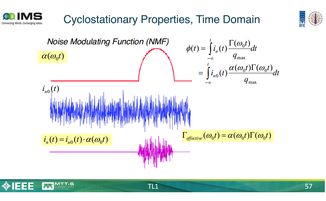
Cyclostationary noise can be viewed as stationary noise, \(i_{n0}(t)\), multiplied by a periodic
envelope, \(\alpha(\omega_0 t)\).
Effective ISF — ISF multiplied with
Noise Modulating Function (NMF)
For Colpitts Oscillator, \(\Gamma_\text{eff}(x)\) is different from
\(\Gamma(x)\), however \(\Gamma_\text{eff}(x)\) and \(\Gamma(x)\) are almost identical for ring
oscillator
alternative derivation
Michael Perrott August 12, 2008, Short Course On Phase-Locked Loops
and Their Applications Day 2, AM Lecture Basic Building Blocks
Voltage-Controlled Oscillators [https://www.cppsim.com/PLL_Lectures/day2_am.pdf]
White Noise Input
1/f Noise in Input Current
Current Noise Modulation
another alternative
derivation
\[
S_{\phi,USB} =
\frac{S_n^{''}}{q_\text{max}^2\Delta\omega^2}\left(a_0^2+\sum_{k\neq0}a_k^2\right)=\frac{S_n^{''}}{q_\text{max}^2\Delta\omega^2}\left(\frac{c_0^2}{4}+\sum_{k=1}^\infty
\frac{c_k^2}{2}\right)=\frac{S_n^{'}}{4q_\text{max}^2\Delta\omega^2}\left(\frac{c_0^2}{2}+\sum_{k=1}^\infty
c_k^2\right)
\] where \(S_n^{''}\) is
two sided PSD, \(S_n^{}\) is one sided
PSD
Diff. Pair Noise with ISF
only half of this current is differentially injected
in the tank at the zero-crossing
Given \(\Gamma_{MOS}\) shown as
above slide \[
F_{rms,MOS}^2 = \frac{1/4\cdot T_\text{w}}{T_0/2} =
\frac{T_\text{w}}{2T_0}
\]
P. Andreani, X. Wang, "On the Phase-Noise and Phase-Error
Performances of Multiphase LC CMOS VCOs," IEEE Journal of Solid-State
Circuits, vol. 39, pp. 1883-1893, Nov. 2004. [https://backend.orbit.dtu.dk/ws/files/4109919/Wang.pdf]
P. Andreani, X. Wang, L. Vandi, A. Frad, "A study of phase noise in
Colpitts and LC-tank CMOS oscillators," IEEE Journal of Solid-State
Circuits, vol. 40, pp. 1107-1118, May 2005. [https://backend.orbit.dtu.dk/ws/files/3976825/Andreani.pdf]
A. Bevilacqua, P. Andreani, "An Analysis of 1/f Noise to Phase Noise
Conversion in CMOS Harmonic Oscillators," IEEE Transactions on Circuits
and Systems I: Regular Papers, vol. 59, no. 5, pp. 938-945, May 2012 [https://sci-hub.jp/10.1109/TCSI.2012.2190564]
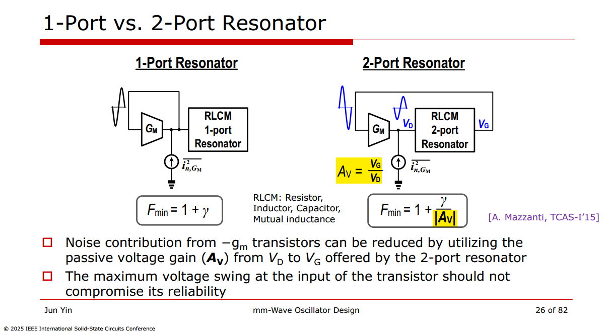
For Class-B with an Ideal Current Source
noise factor is \(\boxed{1+\gamma_n}\)
\(-g_m\) transistors (M1,2) do
not contribute to \(1/f\) noise upconversion
Note the contrast with thermal noise: white
noise is uncorrelated between the two crossings, so the two
kicks don't cancel — their variances add. That's why the same
commutation mechanism gives you the full \(\gamma_n\) term in \(F = 1+\gamma_n\) for the \(1/f^2\) region, yet contributes nothing in
\(1/f^3\)
Closed-Form Formula for the
ISF
If the state variables are node
voltages, write \(\Delta \vec X = \sum_i
\Delta v_i\,\hat e_i\) (with \(\Delta
v_i = \Delta q_i/C_i\)) and the dot product
distributes: \[
\Delta\phi = \frac{2\pi}{T}\frac{\big(\sum_i \Delta v_i \hat
e_i\big)\cdot \dot{\vec X}}{\lVert\dot{\vec X}\rVert^{2}}
\;=\frac{2\pi}{T}\; \sum_i\,\frac{\Delta v_i\, \dot v_i}{\lVert\dot{\vec
X}\rVert^{2}} \;=\; \sum_i \Delta\phi_i,
\] For second-order system, one can use the normalized waveform
and its derivative as the state variables \[
\Gamma_{1}(x)=\frac{f'(x)}{f^{2}(x)+f'^{2}(x)} \qquad
\Gamma_{2}(x)=\frac{f''(x)}{f'^{2}(x)+f''^{2}(x)}
\] In the case of an ideal sinusoidal oscillator \(f=\cos(x)\)\[
\Gamma_{1}(x)=-\sin(x) \qquad \Gamma_{2}(x)=-\cos(x)
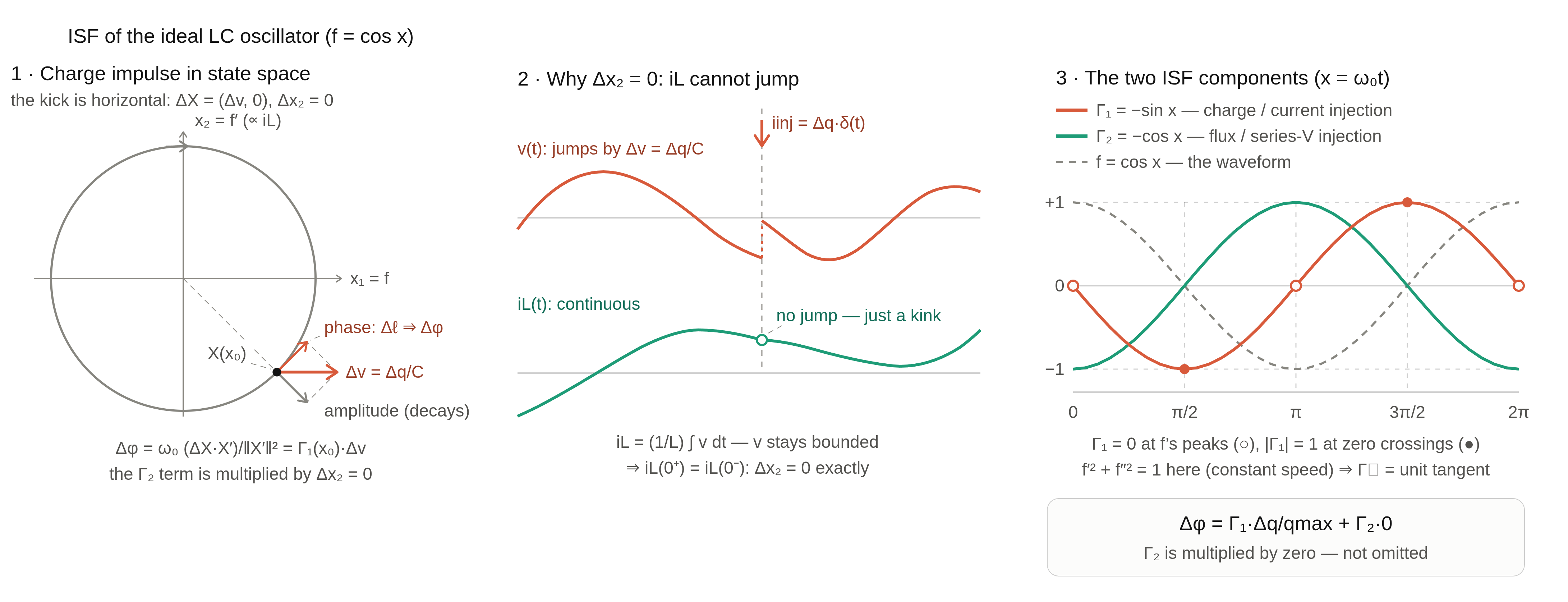
\] A finite charge impulse into the node cannot make the inductor
current jump (\(v\) stays bounded, so
\(i_L=\frac{1}{L}\int v\,dt\) is
continuous) — currentcomponent of the
perturbation is exactly zero. That's physics of
the input, not an approximation: \(\Delta\vec
X = (\Delta v,\,0)\) exactly, so \(\Gamma_2\) gets multiplied by zero
Total phase noise sums over physical sources, each weighted by its
own ISF
If every noise source in the circuit injects current into nodes —
transistor channel noise, resistor noise, the usual on-chip situation —
then the \(\Gamma_1\) family is the
whole story with no approximation
\(\Gamma_2\) enters only when a
source physically acts as a series voltage on the inductor (flux
injection), such as the coil's series resistance
quietly assumes the normal component contributes zero phase
shift, i.e., that surfaces of equal phase (isochrons) cross the limit
cycle orthogonally
Real oscillators violate this to varying degrees (amplitude-to-phase
conversion), which is why the paper ranks direct impulse-injection
simulation as the most accurate
The dot product and norm in (31)–(33) mean different things in
different coordinates, so the same physical oscillator run through (33)
in two different coordinate systems yields two different ISFs — and only
one coordinate choice yields the paper's intended answer
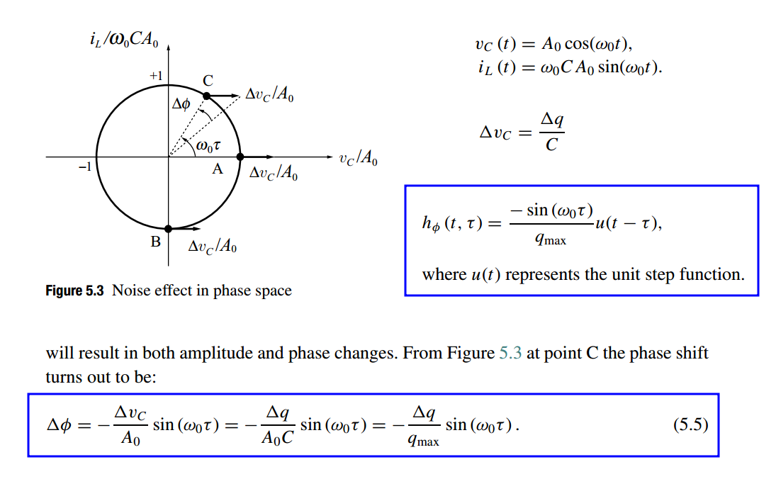
Consider the ideal parallel LC network —
pure sinusoid wave
Suppose a current pulse with area \(q\) suddenly changes the charge across the
capacitor, its voltage changes by \(\Delta
v_c=\Delta q/C\)
Decompose the horizontal kick \(\Delta\vec
r=(\Delta x,0)\) and \(\Delta x=\Delta
v_C/A_0\), with tangential direction \(\hat t=(-\sin\theta,\cos\theta)\) and
radial direction \(\hat
r=(\cos\theta,\sin\theta)\)\[
\Delta \phi = \arctan\left(\frac{\Delta\vec r\cdot \hat t}{1 +
\Delta\vec r\cdot \hat r}\right) = \arctan\left(\frac{-\Delta x \sin
\theta}{1 + \Delta x \cos \theta}\right)\approx -\frac{\Delta v_C}{A_0}
\sin(\omega_0 \tau)
\]
Therefore, the ISF of an ideal parallel LC resonator
can be expressed as \(\boxed{\Gamma(\omega
\tau)=-\sin(\omega_0 \tau)}\), which is independent of peak
voltage value \(A_0\)
C. Calculation of ISF Based on the First
Derivative
additive voltage error
A fixed \(\Delta V\) at a crossing
shifts the crossing time by \(\Delta t =
\Delta V/\dot v\), so \(\Delta\phi =
\omega_0\Delta V/\dot v\). Express this against the normalized
injection \(\Delta\phi = \Gamma\cdot\Delta
V/V_{\max}\) and solve: \[
\Gamma_{\text{crossing}} = \frac{\omega_0 V_{\max}}{\dot v} =
\frac{1}{f'}
\] Now take eq. (37) at the mid-transition, where \(f'' = 0\) (inflection point): \[
\Gamma = \frac{f'}{f'^2 + f''^2}\;\Big|_{f''=0}
= \frac{f'}{f'^2} = \frac{1}{f'}
\]
\[
\boxed{
\text{steeper transition}
\quad\Longrightarrow\quad
\text{smaller ISF peak}
}
\] with \(\Gamma = \sin x\), at
crossing \(\sin x =1\), which is
derivative of edge \[
\Delta \phi = \Gamma \frac{\Delta q}{q_\text{max}} = \sin x\cdot
\frac{\Delta q}{C\cdot A}= \sin x\cdot \frac{\Delta q}{C\cdot A\sin x}
\]
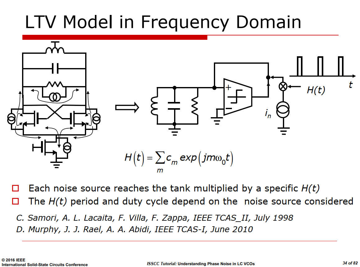
Murphy's Model — LTV in
Frequency Domain
C. Samori, A. L. Lacaita, F. Villa and F. Zappa, "Spectrum folding
and phase noise in LC tuned oscillators," in IEEE Transactions on
Circuits and Systems II: Analog and Digital Signal Processing, vol.
45, no. 7, pp. 781-790, July 1998 [https://sci-hub.ru/10.1109/82.700925]
D. Murphy, J. J. Rael and A. A. Abidi, "Phase Noise in LC
Oscillators: A Phasor-Based Analysis of a General Result and of Loaded Q
," in IEEE Transactions on Circuits and Systems I: Regular Papers, vol.
57, no. 6, pp. 1187-1203, June 2010 [https://sci-hub.ru/10.1109/TCSI.2009.2030110]
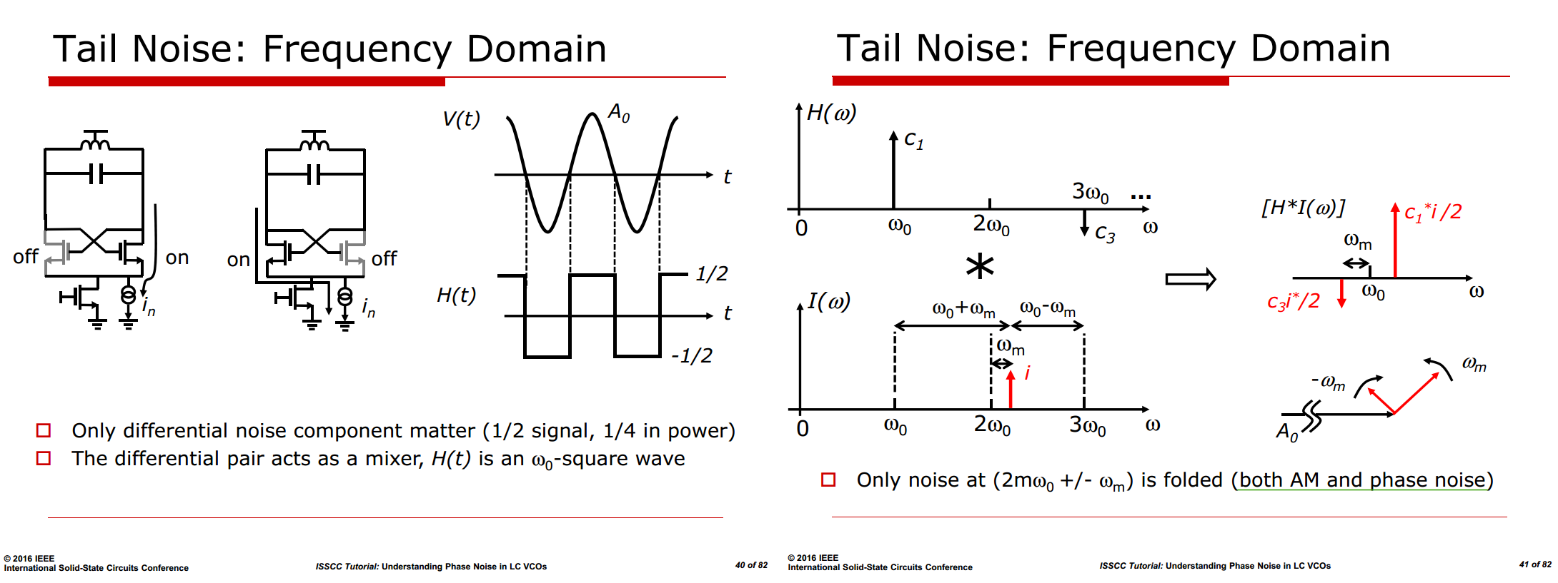
The differential pair plays two distinct roles. Toward its own noise
it acts as a sampling gate — each transistor contributes only within the
short conduction windows at the zero crossings — and the resulting
injection is almost purely phase-modulating.
Toward the tail noise it acts as a single-balanced mixer, commutating
the upstream current with a square wave and folding it as a single
sideband that splits equally into AM and PM
Diff. Pair Noise
For diff. pair noise, the diff. pair is its own noise
gate
half of the noise current of each generator reaches
the tank, while the remaining half circulates within
the transistor
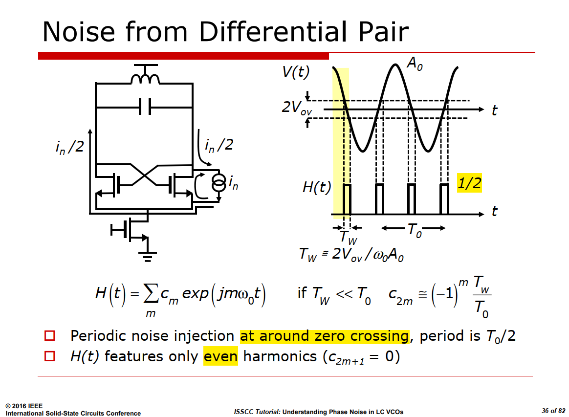
A reference pulse train centered at \(t=0\) would have plain positive
coefficients (\(\tfrac{T_w}{T_0}\),
with \(\operatorname{sinc} \approx
1\)). \[
c_n = \frac{1}{2}\cdot
\frac{T_w}{T_0/2}\operatorname{sinc}\left(\frac{nT_w}{T_0/2}\right)=\frac{T_w}{T_0}\operatorname{sinc}\left(\frac{2nT_w}{T_0}\right)
\] The real injection sits at \(t=T_0/4\), and since the pulse-train period
is \(P=T_0/2\), that offset is exactly
\(P/2\) — a half-period shift. Every
coefficient therefore picks up \((-1)^m\) — \(e^{j2m\omega_0\cdot T_0/4}=e^{jm\pi}\)\[
c_{2m} = \underbrace{(-1)^m}_{\text{position}}\,
\underbrace{\frac{T_w}{T_0}}_{\text{area / period}}\,
\underbrace{\operatorname{sinc}\!\left(\frac{2mT_w}{T_0}\right)}_{\to\,1
\text{ as } T_w \ll T_0}
\]
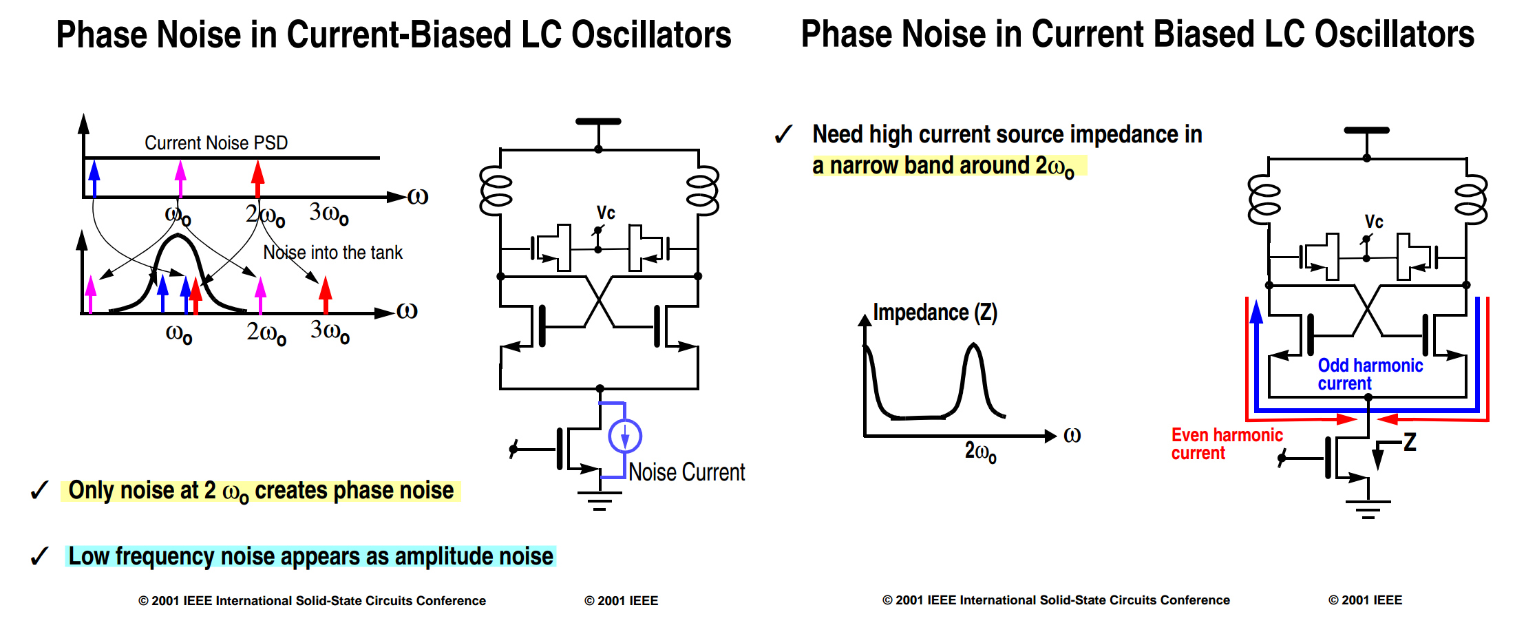
Consequently, excess noise arises solely from the components at \(\omega_0\pm \omega_m\), since all other
spectral components lie outside the tank bandwidth and are therefore
suppressed by the resonator's frequency-selective filtering
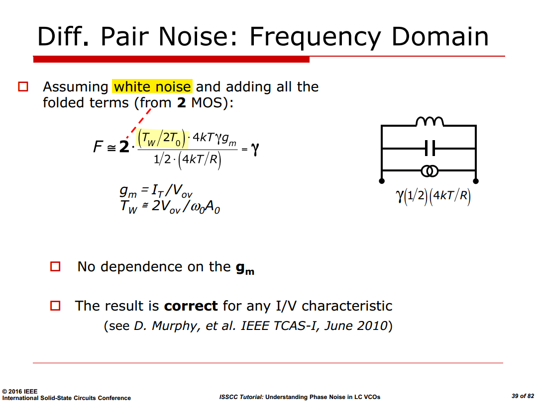
For one MOS, Two-Sided PSD is \[
S_O = S_I \cdot \mathcal{D}\cdot \mathcal{h}^2 = 2kT\gamma g_m\cdot
\frac{2T_W}{T_0}\cdot\frac{1}{4} = \frac{T_W}{2T_0}\cdot 2kT\gamma g_m
\] yield One-Sided PSD of one
MOS\[
S_O' = \textcolor{blue}{\frac{T_W}{2T_0}}\cdot 4kT\gamma g_m
\]
The single-tone analysis establishes that the
differential-pair current is injected as almost pure phase
noise, while summing the white-noise power over all
harmonics of the gating function (\(\overline{H^2}=T_W/2T_0\)) sets its
magnitude; together these yield the differential-pair
contribution to the oscillator phase noise.
phase noise is independent of the transconductance of the
transistors
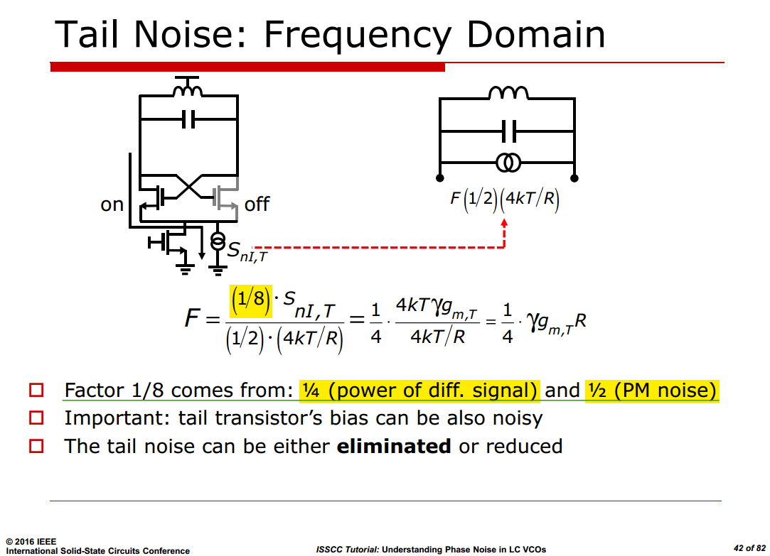
Tail Noise
For the tail noise, the diff. pair is a mixer
\[
V_{AM} = \tfrac{1}{2}\big(C_+ + \overline{C}_-\big) =
\tfrac{1}{2}\Big(\tfrac{c_1^* i}{2} + \tfrac{c_3^* i}{2}\Big)\qquad
V_{PM} = \tfrac{1}{2}\big(C_+ - \overline{C}_-\big) =
\tfrac{1}{2}\Big(\tfrac{c_1^* i}{2} - \tfrac{c_3^* i}{2}\Big)
\]\(V_{AM}\approx V_{PM}\) for
a square wave \(|c_1|=3|c_3|\) —
modulated tail noise is divided into AM and phase noise
almost equally\[
S_{I,PN} = S_{nI,T} \cdot \mathcal{D}\cdot \mathcal{h}^2 \cdot
\frac{1}{2} = S_{nI,T} \cdot 1 \cdot \frac{1}{4}\cdot \frac{1}{2} =
\boxed{\frac{1}{8}\cdot S_{nI,T}}
\] The commutation folds tail noise as a (near) single
sideband, which is equivalent to equal AM and PM — and only the
PM half counts toward phase noise
Noise around \(\boxed{2\omega_0
\pm\omega_m}\) dominate phase noise due to \(|c_1|, |c_3| \gg |c_{2m+1}|
\space\space\space\space \forall m>1\)
E. Hegazi, H. Sjoland and A. Abidi, "A filtering technique to lower
oscillator phase noise," 2001 IEEE International Solid-State
Circuits Conference. Digest of Technical Papers. ISSCC (Cat.
No.01CH37177), San Francisco, CA, USA, 2001 [paper,
slides]
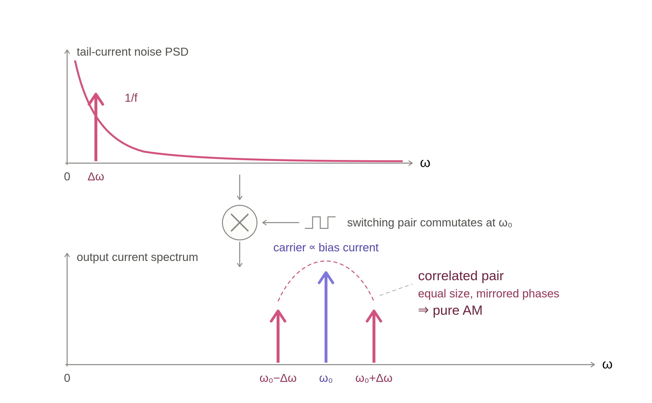
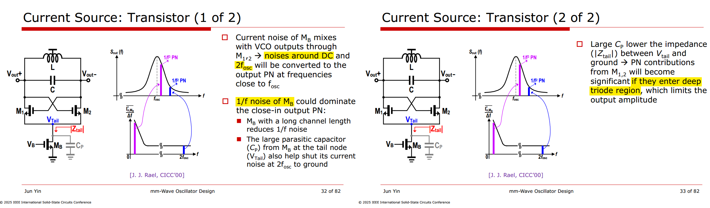
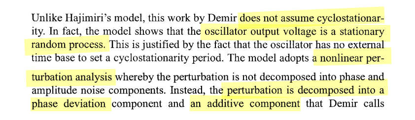
In the first-order, noise around DC (flicker) is
upconverted as a pair of correlated, symmetric
sidebands around the carrier — which is pure AM
practical outcome once second-order conversion effects are
included
flicker near DC → AM/bias modulation → converted to FM →
1/f3 PN (the purple arrow in its spectrum)
while thermal noise at 2fosc → direct PN →
1/f2 PN (the blue arrow)
Demir's Model — NLTV
A. Demir, A. Mehrotra and J. Roychowdhury, "Phase noise in
oscillators: a unifying theory and numerical methods for
characterization," in IEEE Transactions on Circuits and Systems I:
Fundamental Theory and Applications, vol. 47, no. 5, pp. 655-674,
May 2000 [https://sci-hub.jp/10.1109/81.847872]
A. Demir and A. Sangiovanni-Vincentelli, Analysis and Simulation
of Noise in Nonlinear Electronic Circuits and Systems, vol. 425.
Boston, MA, USA: Kluwer Academic Publishers, 1998
A. Mehrotra and A. Sangiovanni-Vincentelli, Noise Analysis of
Radio Frequency Circuits, 1st ed. New York, NY, USA: Springer,
2004
Demir's theory is essentially Floquet theory applied to the limit
cycle of an autonomous oscillator, and the PPV is one specific Floquet
vector
PPV (Perturbation Projection
Vector)
A. Demir and J. Roychowdhury, "A reliable and efficient procedure for
oscillator PPV computation, with phase noise macromodeling
applications," in IEEE Transactions on Computer-Aided Design of
Integrated Circuits and Systems, vol. 22, no. 2, pp. 188-197, Feb.
2003 [https://sci-hub.se/10.1109/TCAD.2002.806599]
S. Levantino and P. Maffezzoni, "Computing the Perturbation
Projection Vector of Oscillators via Frequency Domain Analysis," in IEEE
Transactions on Computer-Aided Design of Integrated Circuits and
Systems, vol. 31, no. 10, pp. 1499-1507, Oct. 2012 [https://sci-hub.se/10.1109/TCAD.2012.2194493]
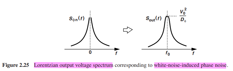
We typically use the two spectra, \(S_{\phi
n}(f)\) and \(S_{out}(f)\),
interchangeably, but we must resolve these inconsistencies.
voltage spectrum is called Lorentzian
spectrum
The periodic signal \(x(t)\) can be
expanded in Fourier series as:
Assume that the signal is subject to excess phase noise,
which is modeled by adding a time-dependent noise
component \(\alpha(t)\). The noisy
signal can be written \(x(t+\alpha(t))\), the added excess phase
\(\phi(t)=
\frac{\alpha(t)}{\omega_0}\)
The autocorrelation of the noisy signal is by definition:
The autocorrelation averaged over time results in:
By taking the Fourier transform of the autocorrelation, the spectrum
of the signal \(x(t + \alpha(t))\) can
be expressed as
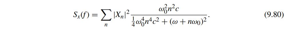
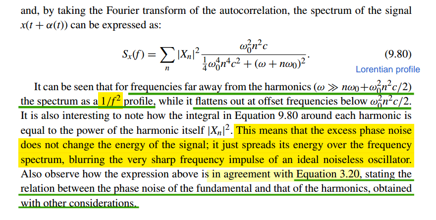
It is also interesting to note how the integral in Equation
9.80 around each harmonic is equal to the power of the harmonic
itself \(|X_n|^2\)
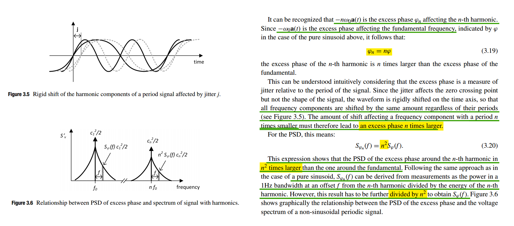
The integral \(S_x(f)\) around
harmonic is \[\begin{align}
P_{x,n} &= \int_{f=-\infty}^{\infty}
|X_n|^2\frac{\omega_0^2n^2c}{\frac{1}{4}\omega_0^4n^4c^2+(\omega
+n\omega_0)^2}df = |X_n|^2\int_{\Delta
f=-\infty}^{\infty}\frac{2\beta}{\beta^2+(2\pi\cdot\Delta f)^2}d\Delta f
\\
&= |X_n|^2\frac{1}{\pi}\arctan(\frac{2\pi \Delta
f}{\beta})|_{-\infty}^{\infty} = |X_n|^2
\end{align}\]
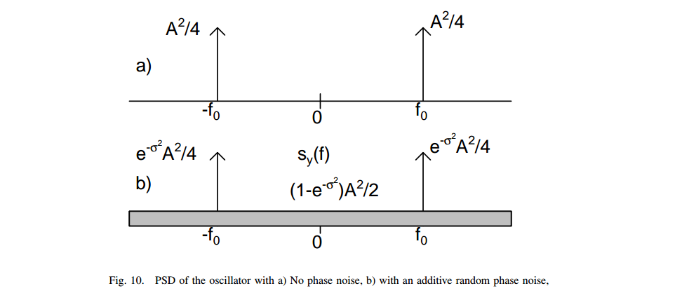
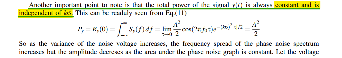
The phase noise does not affect the total power in the
signal, it only affects its distribution
Without phase noise, \(S_v(f)\) is
a series of impulse functions at the harmonics of \(f_o\).
With phase noise, the impulse functions spread, becoming fatter and
shorter but retaining the same total power
A. Mirzaei and A. A. Abidi, "The Spectrum of a Noisy Free-Running
Oscillator Explained by Random Frequency Pulling," in IEEE
Transactions on Circuits and Systems I: Regular Papers, vol. 57,
no. 3, pp. 642-653, March 2010 [https://sci-hub.jp/10.1109/TCSI.2009.2024970]
J. Bank, "A harmonic-oscillator design methodology based on
describing functions," Ph.D. dissertation, Dept. Signals Syst., Sch.
Elect. Eng., Chalmers Univ. Techn., Chalmers, Sweden, 2006. [https://publications.lib.chalmers.se/records/fulltext/17376.pdf]
A. Mazzanti and A. Bevilacqua, "On the Phase Noise Performance of
Transformer-Based CMOS Differential-Pair Harmonic Oscillators," in
IEEE Transactions on Circuits and Systems I: Regular Papers,
vol. 62, no. 9, pp. 2334-2341, Sept. 2015 [https://sci-hub.jp/10.1109/TCSI.2015.2451915]
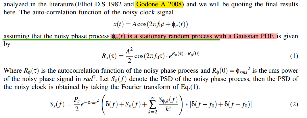
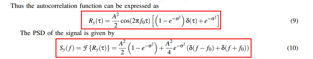
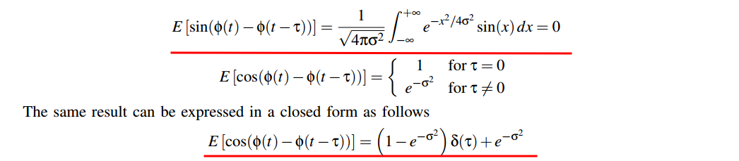
If keep \(\phi_{rms}\) in \(R_x(\tau)\), i.e. \[
R_x(\tau)=\frac{A^2}{2}e^{-\phi_{rms}^2}\cos(2\pi f_0
\tau)e^{R_\phi(\tau)}\approx \frac{A^2}{2}e^{-\phi_{rms}^2}\cos(2\pi f_0
\tau)(1+R_\phi(\tau))
\] The PSD of the signal is \[
S_x(f) = \mathcal{F} \{ R_x(\tau) \} =
\frac{P_c}{2}e^{-\phi_{rms}^2}\left[S_\phi(f+f_0)+S_\phi(f-f_0)\right] +
\frac{P_c}{2}e^{-\phi_{rms}^2}\left[\delta(f+f_0)+\delta(f-f_0)\right]
\] ❗❗above Eq isn't consistent with stationary
white noise process - the following section
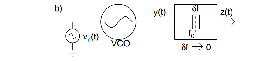
w/ stationary white noise
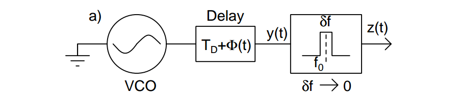
Assuming that the delay line is noiseless
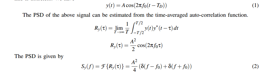
Expanding the cosine function we get \[\begin{align}
R_y(t,\tau) &= \frac{A^2}{2}\left\{\cos(2\pi
f_0\tau)E[\cos(\phi(t)-\phi(t-\tau))] - \sin(2\pi
f_0\tau)E[\sin(\phi(t)-\phi(t-\tau))]\right\} \\
&+ \frac{A^2}{2}\left\{\cos(4\pi
f_0(t+\tau/2-T_D))E[\cos(\phi(t)+\phi(t-\tau))] - \sin(4\pi
f_0(t+\tau/2-T_D))E[\sin(\phi(t)+\phi(t-\tau))] \right\}
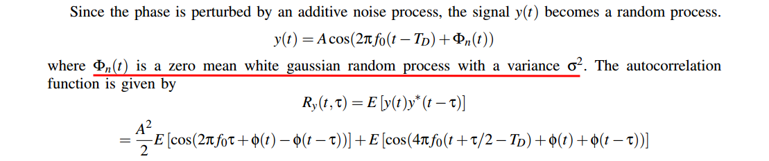
\end{align}\]
where, both the process \(\phi(t)-\phi(t-\tau)\) and \(\phi(t)+\phi(t-\tau)\) are independent of
time \(t\), i.e. \(E[\cos(\phi(t)+\phi(t-\tau))] =
m_{\cos+}(\tau)\), \(E[\cos(\phi(t)-\phi(t-\tau))] =
m_{\cos-}(\tau)\), \(E[\sin(\phi(t)+\phi(t-\tau))] =
m_{\sin+}(\tau)\) and \(E[\sin(\phi(t)-\phi(t-\tau))] =
m_{\sin-}(\tau)\)
The second term in the above expression is periodic in \(t\) and to estimate its PSD, we compute the
time-averaged autocorrelation function\[
R_y(\tau) = \frac{A^2}{2}\left\{\cos(2\pi f_0\tau)m_{\cos-}(\tau) -
\sin(2\pi f_0\tau)m_{\sin-}(\tau)\right\}
\]
After nontrivial derivation
w/ Weiner process
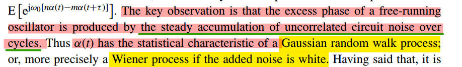
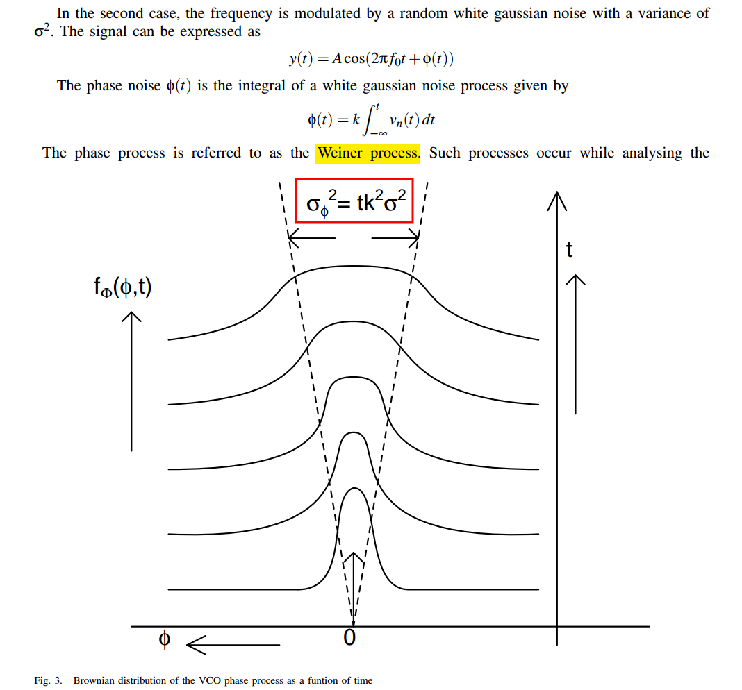
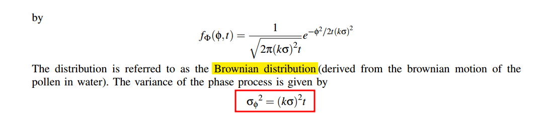
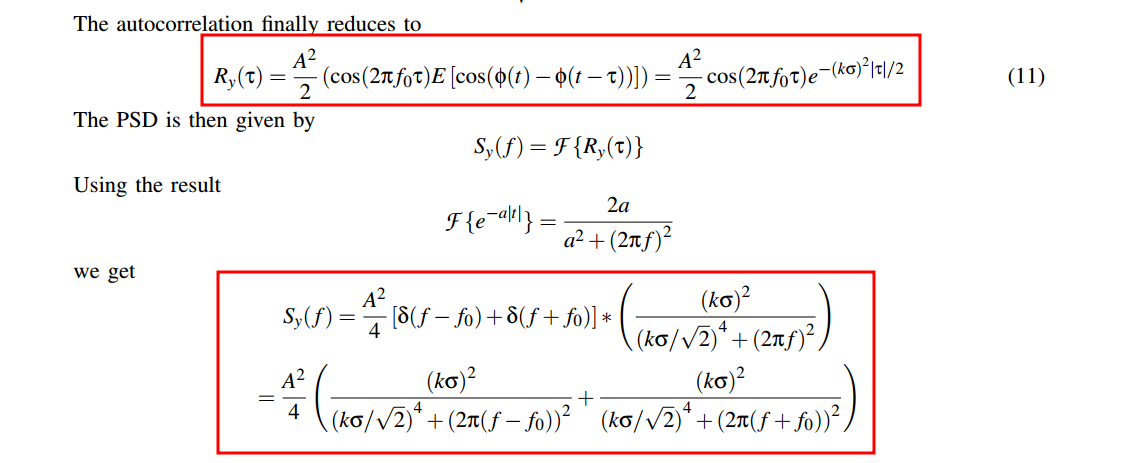
The phase process \(\phi(t)\) is
also gaussian but with an increasing variance which
grows linearly with time\(t\)
The spectrum of \(y(t)\) is
determined by the asymptotic behavior of \(R_y(t,\tau)\) as \(t\to \infty\)
❗❗ \(\lim_{t\to\infty}R_y(t,\tau)\) rather than
time-averaged autocorrelation function of cyclostationary
process, ref. Demir's paper
We define \(\zeta(t,
\tau)=\phi(t)+\phi(t-\tau) = \phi(t)-\phi(t-\tau) +
2\phi(t-\tau)\), the expected value of \(\zeta(t,\tau)\) is 0, the variance is \(\sigma_{\zeta}^2=(k\sigma)^2(\tau +
4(t-\tau))=(k\sigma)^2(4t-3\tau)\)\[
E[\cos(\zeta(t,\tau))]=\frac{1}{\sqrt{2\pi
\sigma_{\zeta}^2}}\int_{-\infty}^{\infty}e^{-\zeta^2/2\sigma_{\zeta}^2}\cos(\zeta)d\zeta
= e^{-\sigma_{\zeta}^2/2}=e^{-(k\sigma)^2(4t-\tau)}
\] i.e., \(\lim _{t\to \infty}
E[\cos(\zeta(t,\tau))] = \lim_{t\to \infty}e^{-(k\sigma)^2(4t-\tau)} =
0\)
For \(E[\sin(\zeta(t,\tau))]\), we
have \[
E[\sin(\zeta(t,\tau))] = \frac{1}{\sqrt{2\pi
\sigma_{\zeta}^2}}\int_{-\infty}^{\infty}e^{-\zeta^2/2\sigma_{\zeta}^2}\sin(\zeta)d\zeta
\] i.e., \(E[\sin(\zeta(t,\tau))]\) is odd
function, therefore \(E[\sin(\zeta(t,\tau))]=0\)
\(\Delta t\) should be measured
after the amplitude settles down (steady-state solution).
The impulse should be injected after the oscillator stabilizes.
The simulation step size used to measure \(\Delta t\) should be small.
The transient-simulation error tolerance should be small.
Use cross function to find zero crossing when impulse is
off. Set significant digits to 16 and note down the value. \[
T_{i=0}
=
15.62239156\times10^{-9}
=
15.622\times10^{-9}
+
0.39156\times10^{-12}
\]
Subtract it from the cross output. ADE output truncates
it, so break it up into different unit scales.
Check that the output is approximately zero before running
sweeps.
Oscillator Injection Linearity
time shift by sweeping current pulse
delay
Aditya Varma Muppala, Noise Modulation Function
(NMF) Simulation in Cadence | Oscillators 08 | MMIC 13
[https://youtu.be/CvcLG9cSreg]
[code]
source-specific ISF
For example, if MOS drain thermal noise is represented as a current
source between drain and source, then the perturbation used to obtain
the source-specific ISF should also be injected between those same drain
and source nodes
NMF \(\alpha_{NMF}(t)\)
shall work with the corresponding source-specific
ISF/PPV
Hu, Yizhe, "Intuitive Understanding of Flicker Noise Reduction via
Narrowing of Conduction Angle in Voltage-Biased Oscillators," in IEEE
Transactions on Circuits and Systems II: Express Briefs, vol. 66, no.
12, pp. 1962-1966, Dec. 2019 [https://sci-hub.ru/10.1109/TCSII.2019.2896483]
—. (2019). A Simulation Technique of Impulse Sensitivity Function
(ISF) Based on Periodic Transfer Function (PXF).
10.13140/RG.2.2.32151.60323. [link]
—, "Oscillator Flicker Phase Noise: A Tutorial," in IEEE
Transactions on Circuits and Systems II: Express Briefs, vol. 68,
no. 2, pp. 538-544, Feb. 2021 [paper]
[slides]
Aditya Varma Muppala, Fast Simulation of ISF and PPV using PSS and
PXF in Cadence | Oscillators 12 | MMIC 19 [videonotecode]
freqaxis=in
PXF preserves the signed input-frequency axis. Therefore, both
positive- and negative-frequency input sidebands can be used directly to
extract the ISF
freqaxis=absin (default)
Positive sidebands can be used directly. For negative sidebands, the
PXF result corresponds to the Hermitian-symmetric positive-frequency
response and must first be complex-conjugated; equivalently, retain its
magnitude and reverse its phase
time reference between tran simulation and pss/pxf is different,
that's why circshift is used.
Using a complex exponential representation gives the same result as
the cosine derivation in the slides, provided the Fourier coefficient
conventions are handled consistently.
The complex-exponential derivation is algebraically simpler than the
cosine derivation. The only subtlety is the Fourier-series
convention:
Positive-frequency coefficient of a cosine: \[
H_k=\frac{h_k}{2}e^{j\theta_{h,k}}.
\]
Fundamental voltage phasor: \[
V_{H1}=\frac{V_{h1}}{2}e^{j\theta}.
\]
Accounting for these \(1/2\) factors
yields the identical PXF expression derived in the slides.
PPV from PSS inbuilt solver
Aditya Varma Muppala, Fast Simulation of ISF and PPV using PSS and
PXF in Cadence | Oscillators 12 | MMIC 19 [https://youtu.be/Lu6VEWEEdxo]
TODO 📅
effective ISF
thermal noise with NMF
source-specific ISF + its NMF
flicker noise with effective
non-normalized ISF
Y. Hu, T. Siriburanon and R. B. Staszewski, "A Low-Flicker-Noise
30-GHz Class-F23 Oscillator in 28-nm CMOS Using Implicit Resonance and
Explicit Common-Mode Return Path," in IEEE Journal of Solid-State
Circuits, vol. 53, no. 7, pp. 1977-1987, July 2018 [https://ieeexplore.ieee.org/stamp/stamp.jsp?tp=&arnumber=8345650]
With the paper’s implicit \(1\text{-Hz}\) noise bandwidth, Eq.
(3) \[
v_{1/f}(t)
=
\sqrt{2}\,V_{1/f,\mathrm{rms}}
\cos(\Delta\omega t+\gamma)
\] represents one narrowband sinusoidal noise component.
Here: \[
V_{1/f,\mathrm{rms}}
=
\sqrt{S_{v,1/f}(\Delta f)\cdot 1\,\mathrm{Hz}}
\] is the RMS voltage amplitude of that
component. Therefore, strictly within Eq. (3), \[
[V_{1/f,\mathrm{rms}}]=\mathrm V.
\] Because the bandwidth is implicitly \(1\,\mathrm{Hz}\), its numerical value
equals the amplitude spectral density expressed in \(\mathrm{V}/\sqrt{\mathrm{Hz}}\): \[
V_{1/f,\mathrm{rms}}[\mathrm V]
\overset{B=1\,\mathrm{Hz}}{=}
\sqrt{S_{v,1/f}}
\left[\frac{\mathrm V}{\sqrt{\mathrm{Hz}}}\right]
\sqrt{1\,\mathrm{Hz}}.
\] Also, more precisely:
\(\Delta\omega t+\gamma\) is the
phase of the sinusoidal component.
\(\cos(\Delta\omega t+\gamma)\) is
the dimensionless sinusoidal waveform.
\(\gamma\) is the random initial
phase.
\(\sqrt{2}V_{1/f,\mathrm{rms}}\) is
the peak amplitude.
Indeed, \[
\operatorname{rms}
\left\{
\sqrt{2}V_{1/f,\mathrm{rms}}
\cos(\Delta\omega t+\gamma)
\right\}
=
V_{1/f,\mathrm{rms}}.
\] Therefore, the same interpretation applies to Eq. (4): \[
i_{1/f,\mathrm{cyclo}}(t)
=
\sqrt{2}I_{1/f,\mathrm{rms}}(t)
\cos(\Delta\omega t+\gamma).
\] Under the implicit \(1\text{-Hz}\) bandwidth, \[
[I_{1/f,\mathrm{rms}}(t)]=\mathrm A,
\] From Eq. (4), \[
i_{1/f,\mathrm{cyclo}}(t)
=
\sqrt{2}\,I_{1/f,\mathrm{rms}}(t)
\cos(\Delta\omega t+\gamma).
\] Substitute this into the phase perturbation integral: \[
\begin{aligned}
\phi(t)
&=
\int_{-\infty}^{t}
h_{\mathrm{DS}}(\tau)
i_{1/f,\mathrm{cyclo}}(\tau)\,d\tau
\\
&=
\sqrt{2}
\int_{-\infty}^{t}
h_{\mathrm{DS}}(\tau)
I_{1/f,\mathrm{rms}}(\tau)
\cos(\Delta\omega\tau+\gamma)\,d\tau.
\end{aligned}
\] Define the periodically varying effective ISF
as \[
\color{blue}\boxed{h_{\mathrm{eff}}(t)
\equiv
h_{\mathrm{DS}}(t)I_{1/f,\mathrm{rms}}(t)}
\] Therefore, \[
\phi(t)
=
\sqrt{2}
\int_{-\infty}^{t}
h_{\mathrm{eff}}(\tau)
\cos(\Delta\omega\tau+\gamma)\,d\tau.
\] Since \(h_{\mathrm{eff}}(t)\)
is periodic with period \(T=2\pi/\omega_0\), write \[
h_{\mathrm{eff}}(t)
=
h_{\mathrm{eff,dc}}
+
\sum_{k=1}^{\infty}
H_k\cos(k\omega_0t+\psi_k),
\] where \[
h_{\mathrm{eff,dc}}
=
\frac{1}{T}
\int_0^T
h_{\mathrm{eff}}(t)\,dt
=
\frac{1}{T}
\int_0^T
h_{\mathrm{DS}}(t)
I_{1/f,\mathrm{rms}}(t)\,dt.
\] This is Eq. (7).
Substitution gives \[
\begin{aligned}
\phi(t)
={}&
\sqrt{2}h_{\mathrm{eff,dc}}
\int^t\cos(\Delta\omega\tau+\gamma)\,d\tau
\\
&+
\sqrt{2}\sum_{k=1}^{\infty}H_k
\int^t
\cos(k\omega_0\tau+\psi_k)
\cos(\Delta\omega\tau+\gamma)\,d\tau.
\end{aligned}
\] The first term is \[
\sqrt{2}h_{\mathrm{eff,dc}}
\int^t\cos(\Delta\omega\tau+\gamma)\,d\tau
=
\frac{\sqrt{2}h_{\mathrm{eff,dc}}}{\Delta\omega}
\sin(\Delta\omega t+\gamma).
\] For the harmonic terms, use \[
\cos A\cos B
=
\frac{1}{2}\left[\cos(A+B)+\cos(A-B)\right].
\] Thus, the exact harmonic contribution is \[
\begin{aligned}
\phi_k(t)
=
\frac{\sqrt{2}H_k}{2}
\Bigg[
&
\frac{
\sin\!\left[(k\omega_0+\Delta\omega)t+\psi_k+\gamma\right]
}{
k\omega_0+\Delta\omega
}
\\
+&
\frac{
\sin\!\left[(k\omega_0-\Delta\omega)t+\psi_k-\gamma\right]
}{
k\omega_0-\Delta\omega
}
\Bigg].
\end{aligned}
\] These terms lie near \(k\omega_0\pm\Delta\omega\), whereas the DC
term produces a slowly varying phase component directly at \(\Delta\omega\).
Because \[
\Delta\omega\ll\omega_0,
\] the slow component is also much larger after integration:
\[
\frac{1}{\Delta\omega}
\gg
\frac{1}{k\omega_0\pm\Delta\omega}.
\] Therefore, keeping only the dominant low-frequency phase term,
\[
\color{blue}\boxed{
\phi(t)
\approx
\frac{\sqrt{2}h_{\mathrm{eff,dc}}}{\Delta\omega}
\sin(\Delta\omega t+\gamma)
}
\] The essential mechanism is \[
\underbrace{h_{\mathrm{DS}}(t)}_{\text{periodic ISF}}
\,
\underbrace{I_{1/f,\mathrm{rms}}(t)}_{\text{periodic noise amplitude}}
\longrightarrow
\underbrace{h_{\mathrm{eff,dc}}}_{\text{nonzero average}},
\]
M. Shahmohammadi, M. Babaie and R. B. Staszewski, "A 1/f Noise
Upconversion Reduction Technique for Voltage-Biased RF CMOS
Oscillators," in IEEE Journal of Solid-State Circuits, vol. 51, no. 11,
pp. 2610-2624, Nov. 2016 [https://pure.tudelft.nl/ws/portalfiles/portal/30880387/07571191.pdf]
References
Jun Yin. ISSCC 2025 T10: mm-Wave Oscillator Design
Pietro Andreani. ISSCC 2011 T1: Integrated LC oscillators
—. "Harmonic Oscillators in CMOS—A Tutorial Overview," in IEEE Open
Journal of the Solid-State Circuits Society, vol. 1, pp. 2-17, 2021 [pdf]
C. Samori, ISSCC2016 T1 "Tutorial: Understanding Phase Noise in LC
VCOs"
—, "Understanding Phase Noise in LC VCOs: A Key Problem in RF
Integrated Circuits," in IEEE Solid-State Circuits Magazine,
vol. 8, no. 4, pp. 81-91, Fall 2016 [https://sci-hub.ru/10.1109/MSSC.2016.2573979]
Jaeha Kim. Lecture 8. Special Topics: Design Trade -Offs in LC -Tuned
Oscillators
Lacaita, Andrea Leonardo, Salvatore Levantino, and Carlo Samori.
Integrated frequency synthesizers for wireless systems.
Cambridge University Press, 2007.
Darabi H. Radio Frequency Integrated Circuits and Systems. 2nd ed.
Cambridge University Press; 2020.
Hegazi, Emad, Asad Abidi, and Jacob Rael. The Designer's Guide to
High-purity Oscillators. [New York]: Kluwer Academic Publishers,
2005. The Designer's Guide to High-Purity Oscillators
Bae, Woorham, and Deog-Kyoon Jeong. Analysis and Design of CMOS
Clocking Circuits for Low Phase Noise. Institution of Engineering
and Technology, 2020.
proportional term (P) depends on the present error
integral term (I) depends on past errors
derivative term (D) depends on anticipated future errors
PID controller makes use of linear extrapolation of
the measured output
PI controller does not make use of any prediction of
the future state of the system
The prediction by linear extrapolation (D) can
generate large undesired control signals because measurement noise is
amplified, that's why D is not used widely
The Problem of
"Sinusoids Running Around Loops"
The representative of Fourier transform \(\frac{1}{j\omega+j\omega_0}\) back in the
time domain \(e^{-j\omega_0 t}\) is
infinite extent in time
Running around a loop, chasing one's tail — these are thought
pictures that only work in a discretized, time-sequenced conceptual
framework that has a beginning and an end
Fix in your mind that oscillations are a type of
resonance
System Type
Control of Steady-State Error to Polynomial Inputs: System Type
control systems are assigned a type number according
to the maximum degree of the input polynominal for which the
steady-state error is a finite constant. i.e.
Type 0: Finite error to a step (position error)
Type 1: Finite error to a ramp (velocity error)
Type 2: Finite error to a parabola (acceleration error)
If we consider tracking the reference input alone and set \(W = V = 0\)
The open-loop transfer function can be expressed as
\[
T(s) = \frac{K_n(s)}{s^n}
\]
where we collect all the terms except the pole (\(s\)) at eh origin into \(K_n(s)\),
The polynomial inputs, \(r(t)=\frac{t^k}{k!} u(t)\), whose transform
is \[
R(s) = \frac{1}{s^{k+1}}
\]
Then the equation for the error, \(R(s)-Y(s)\) is simply \[
E(s) = \frac{1}{1+T(s)}R(s)
\]
Application of the Final Value Theorem to the error formula
gives the result
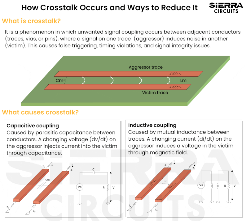
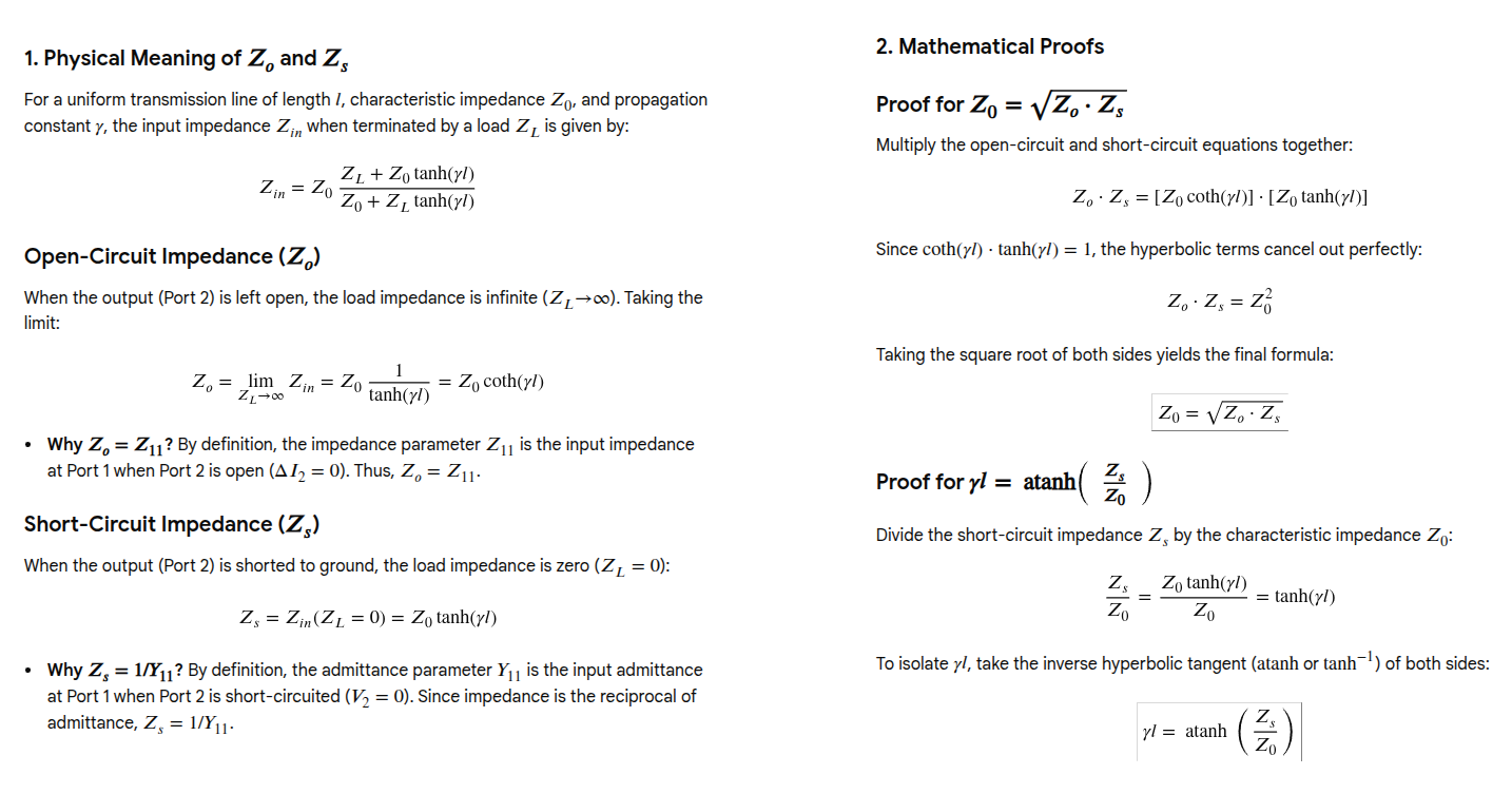
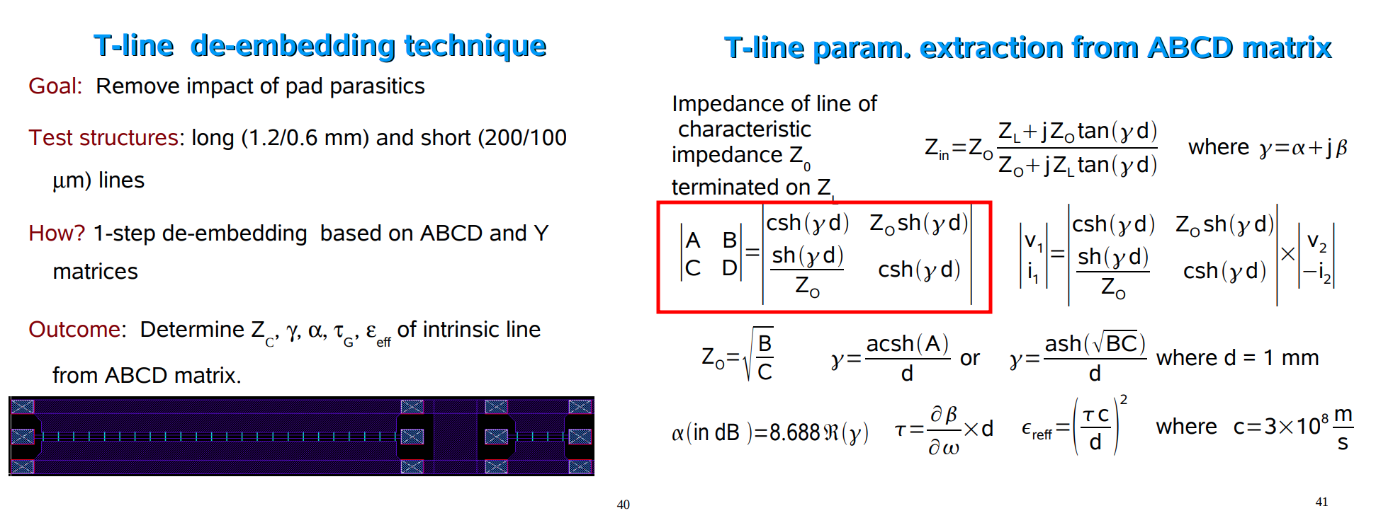
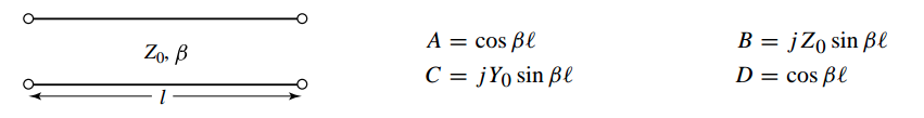
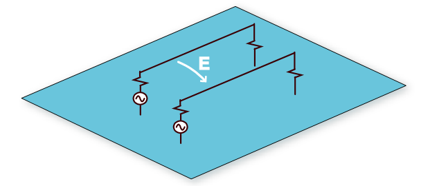
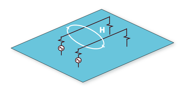
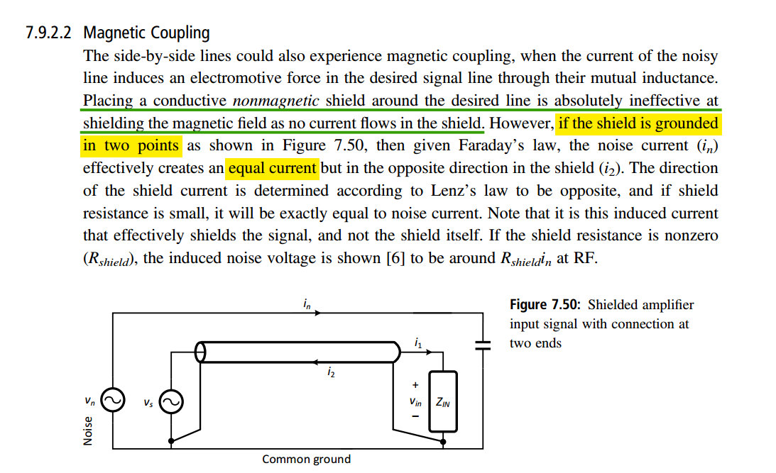

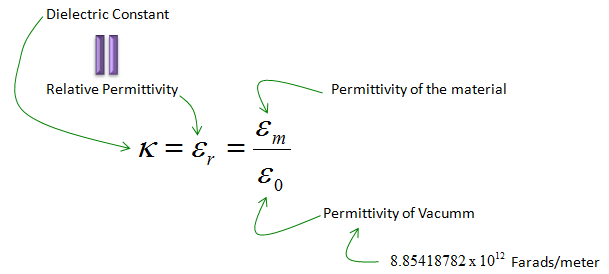
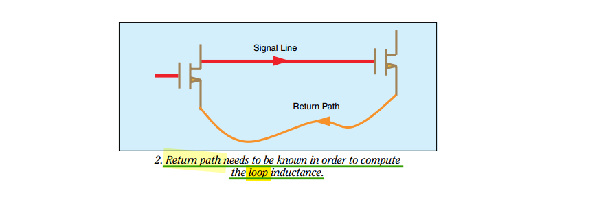
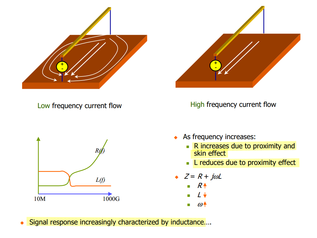
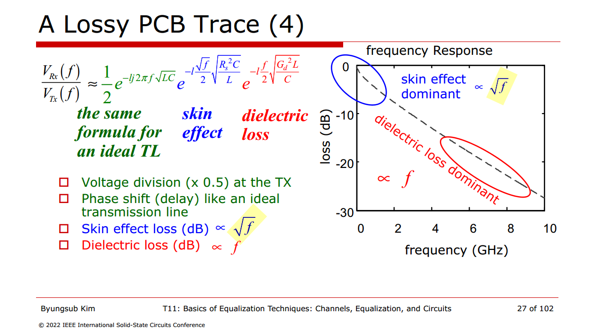
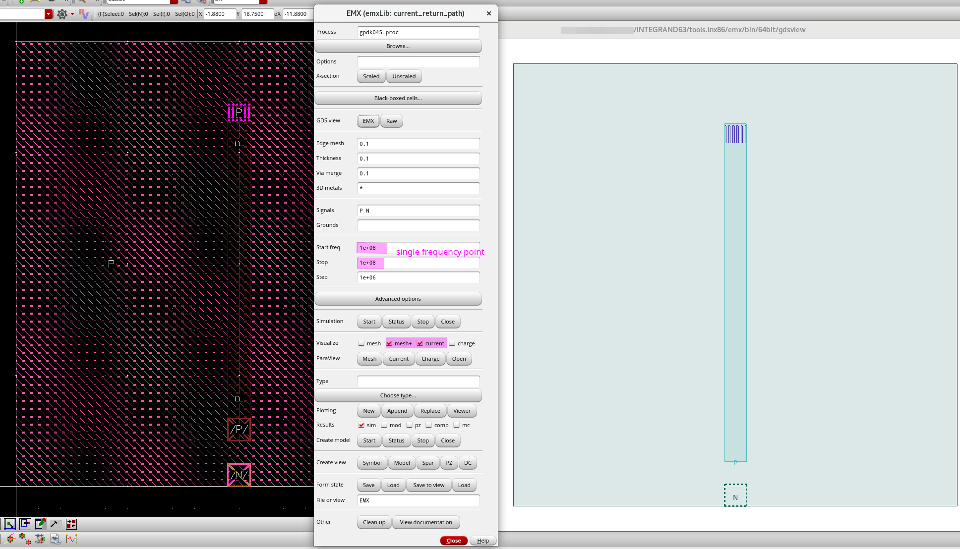
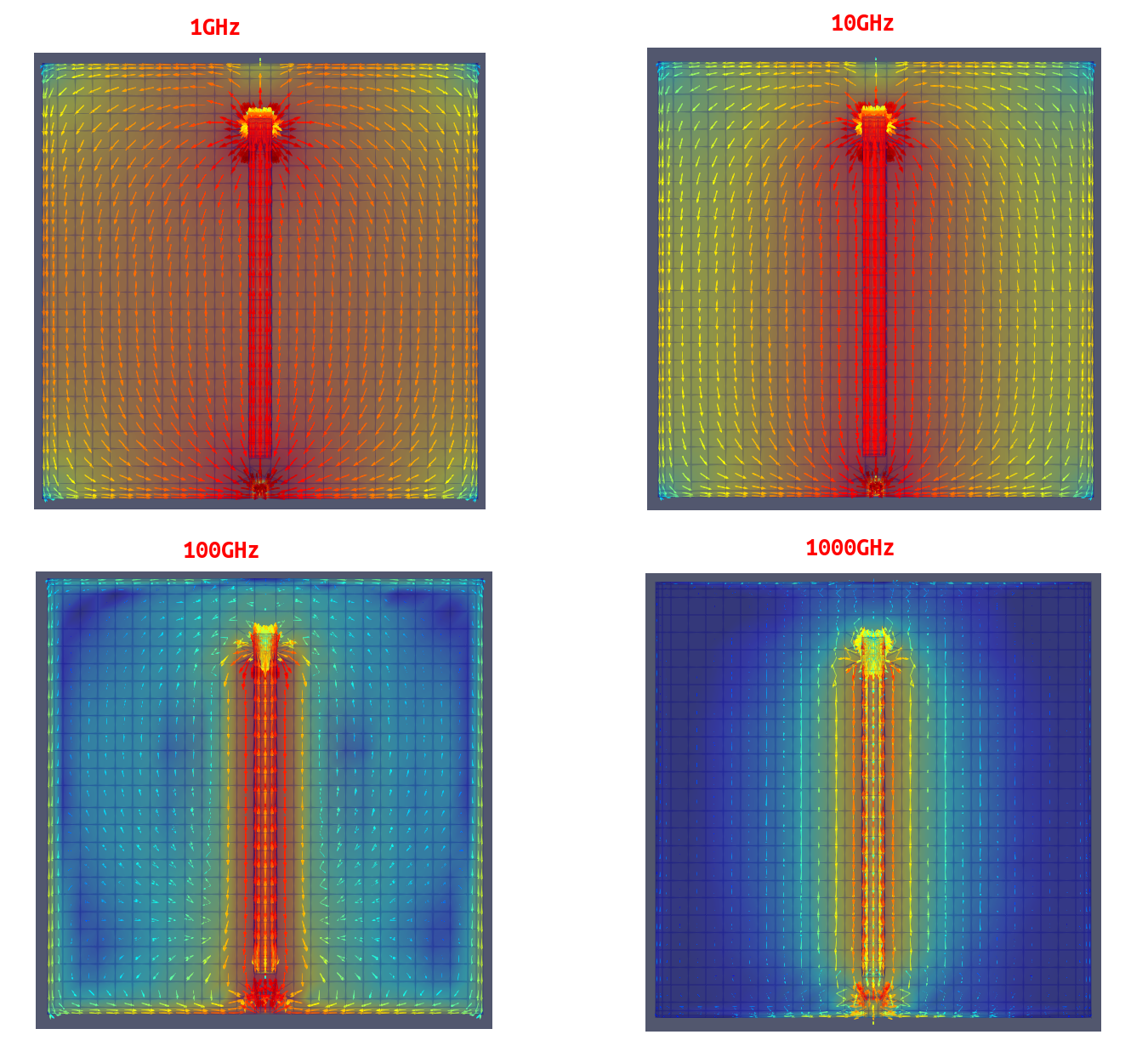
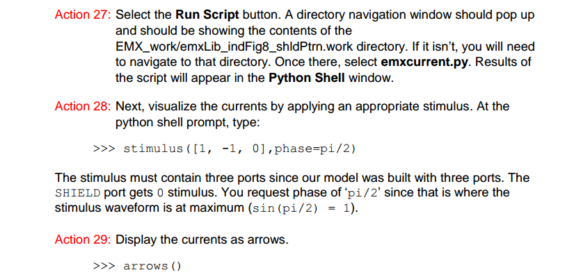
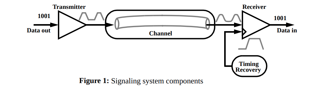
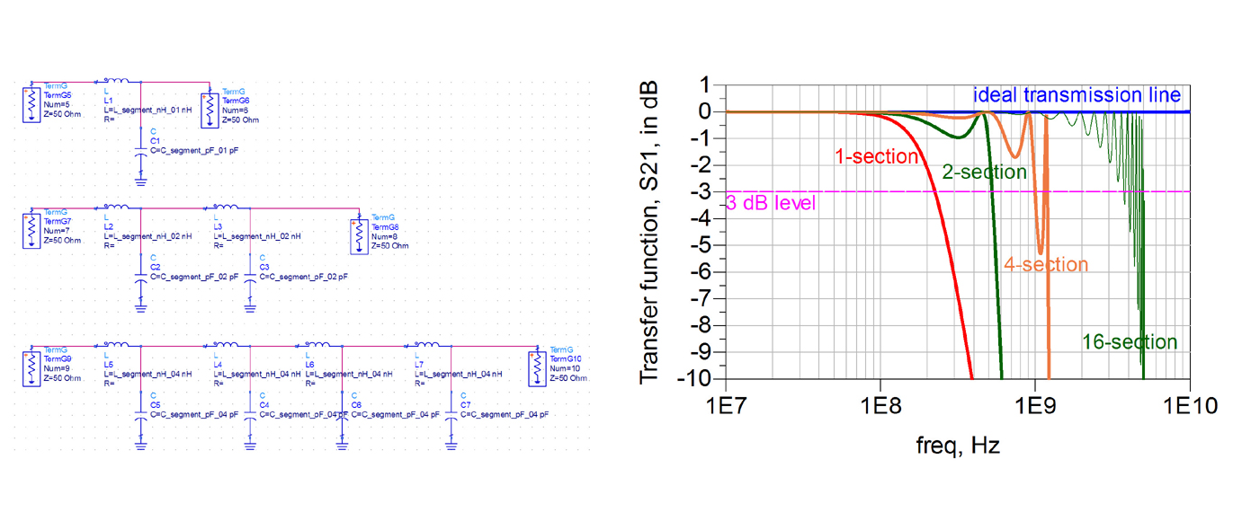
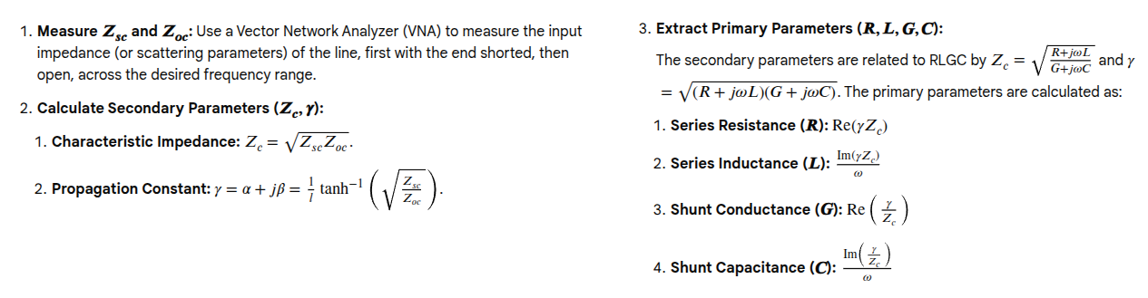
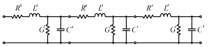 \[
\boxed{R= \text{Re}(\gamma Z_c)} \qquad
\boxed{L= \frac{\text{Im}(\gamma Z_c)}{\omega}} \qquad
\boxed{G= \text{Re}\left(\frac{\gamma}{Z_c}\right)} \qquad
\boxed{C= \frac{\text{Im}\left(\frac{\gamma}{Z_c}\right)}{\omega}}
\]
\[
\boxed{R= \text{Re}(\gamma Z_c)} \qquad
\boxed{L= \frac{\text{Im}(\gamma Z_c)}{\omega}} \qquad
\boxed{G= \text{Re}\left(\frac{\gamma}{Z_c}\right)} \qquad
\boxed{C= \frac{\text{Im}\left(\frac{\gamma}{Z_c}\right)}{\omega}}
\]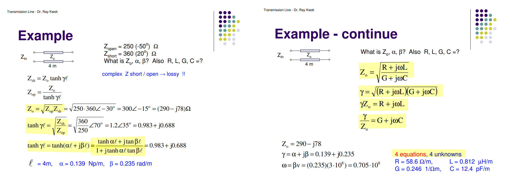
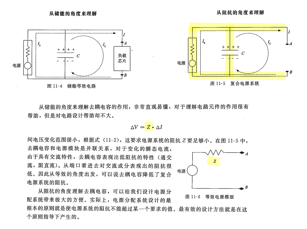
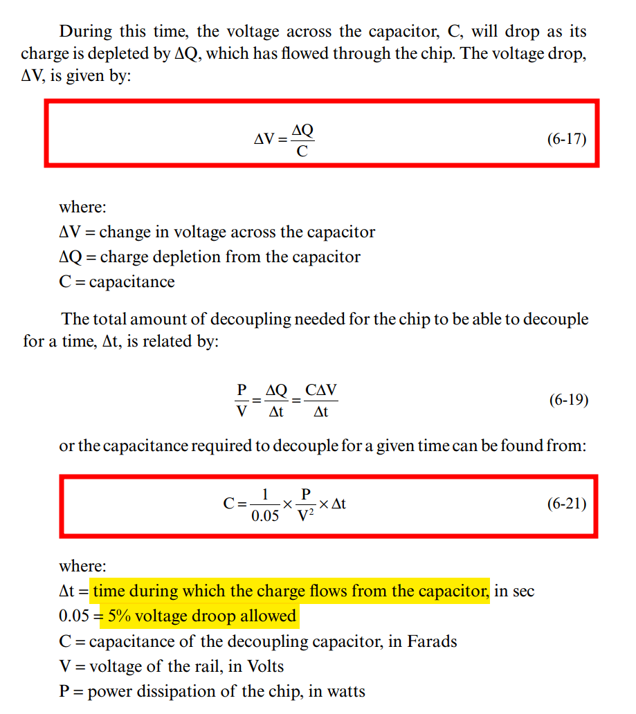
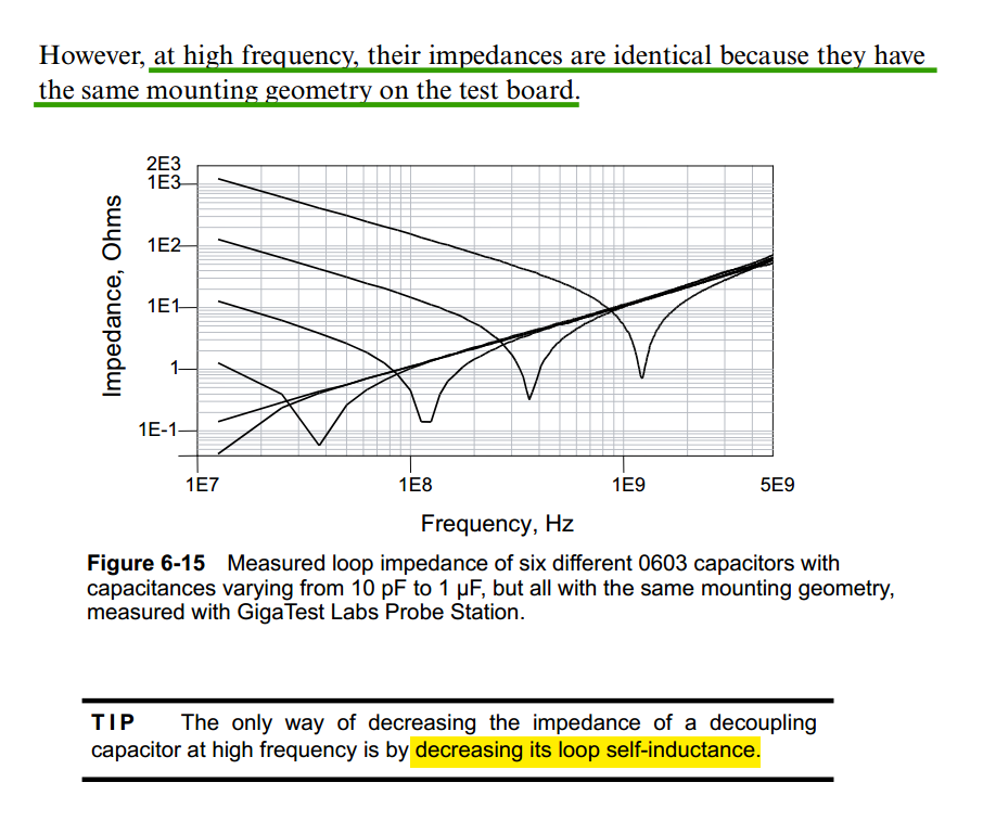
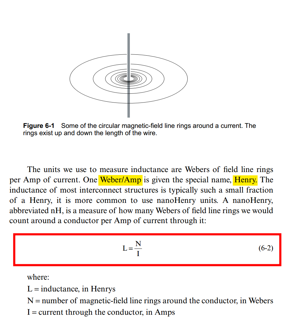
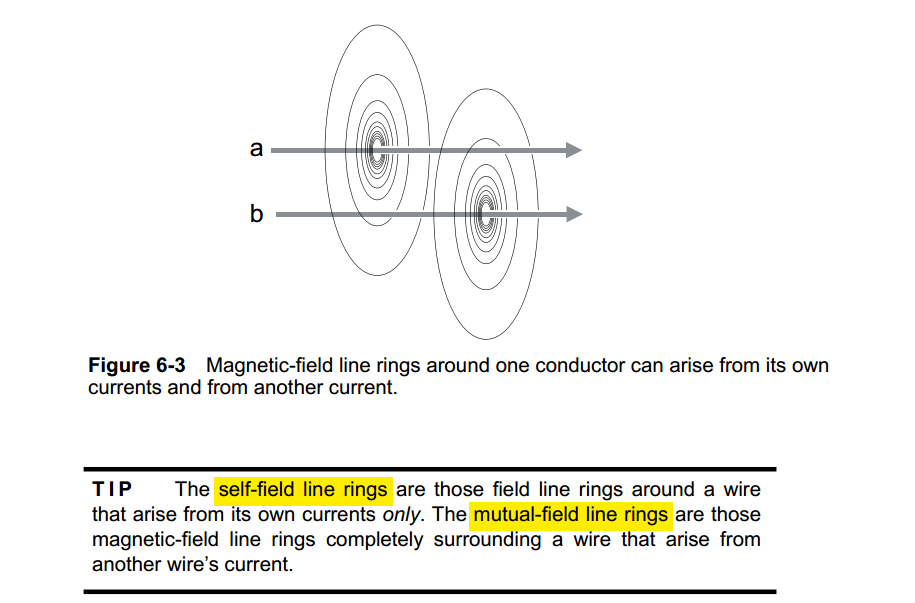
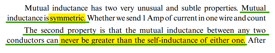
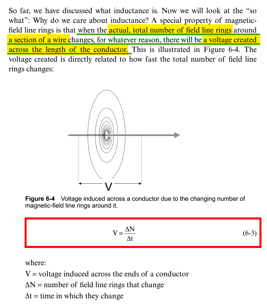
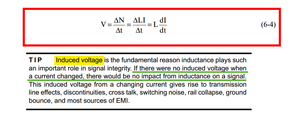
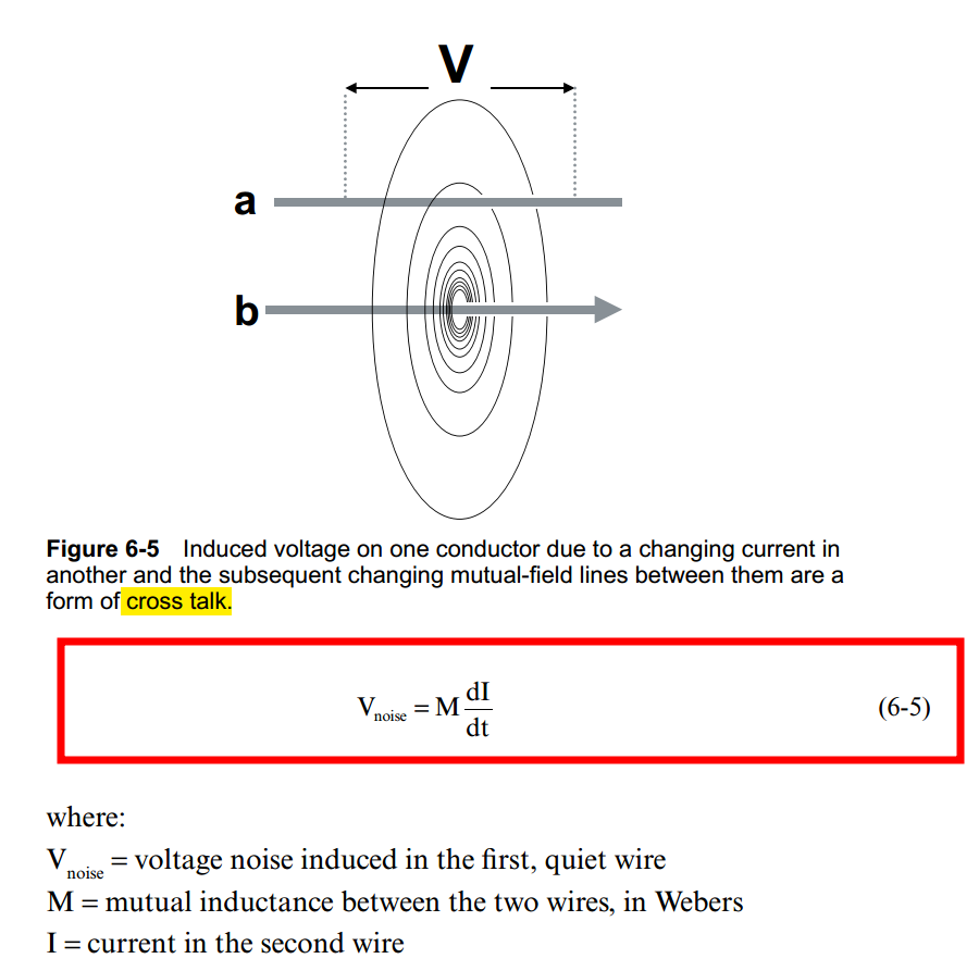
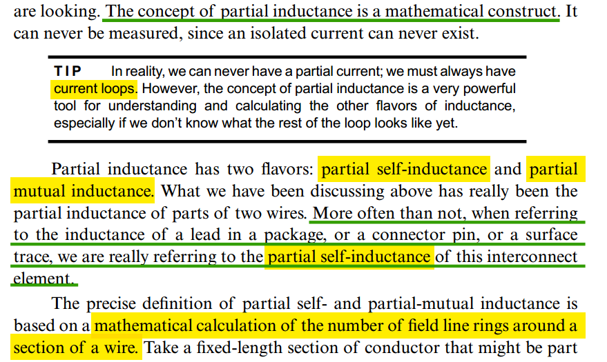
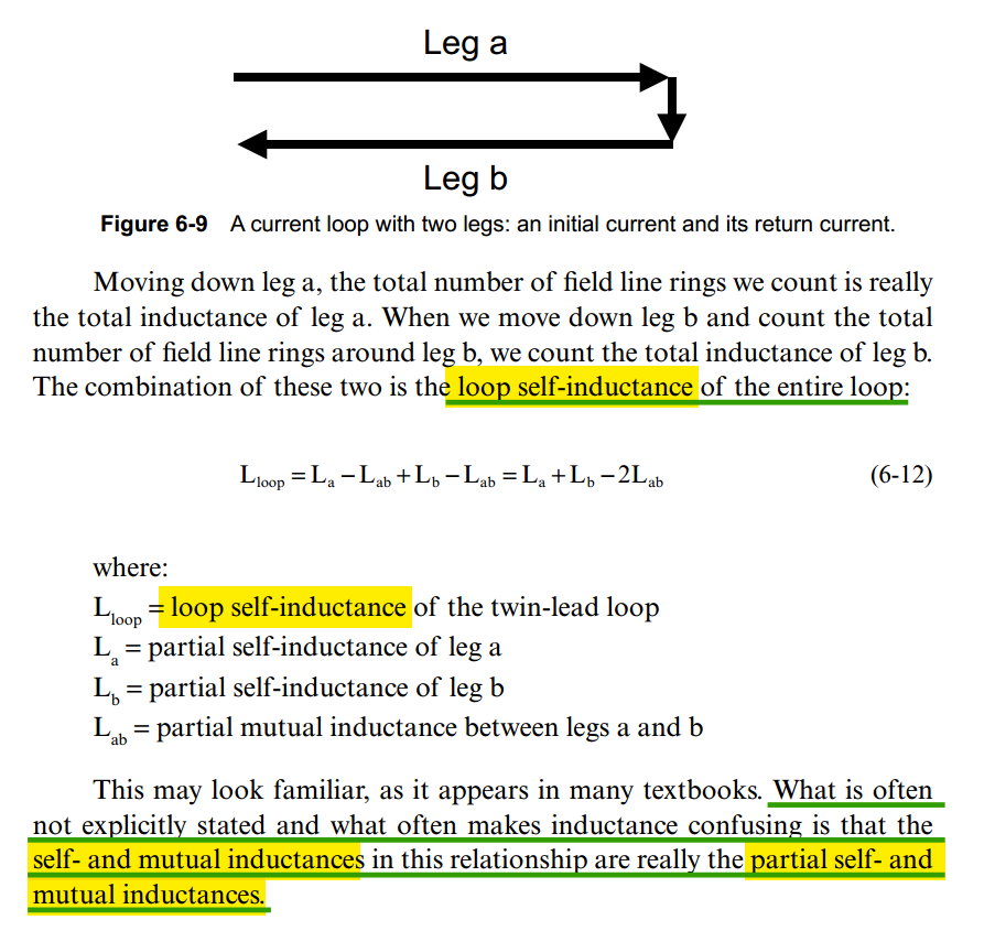
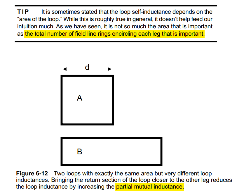
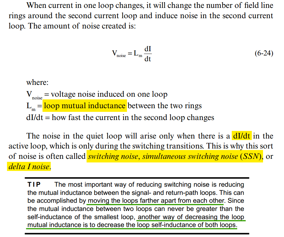
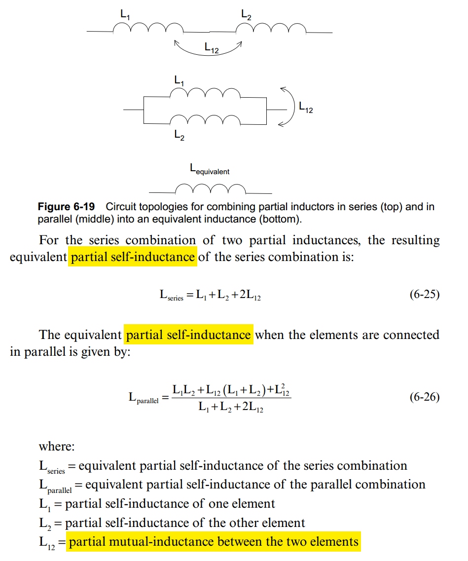
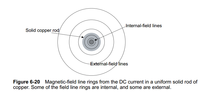
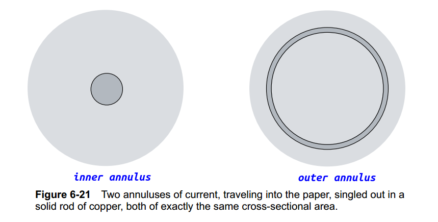
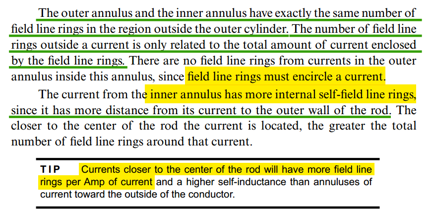
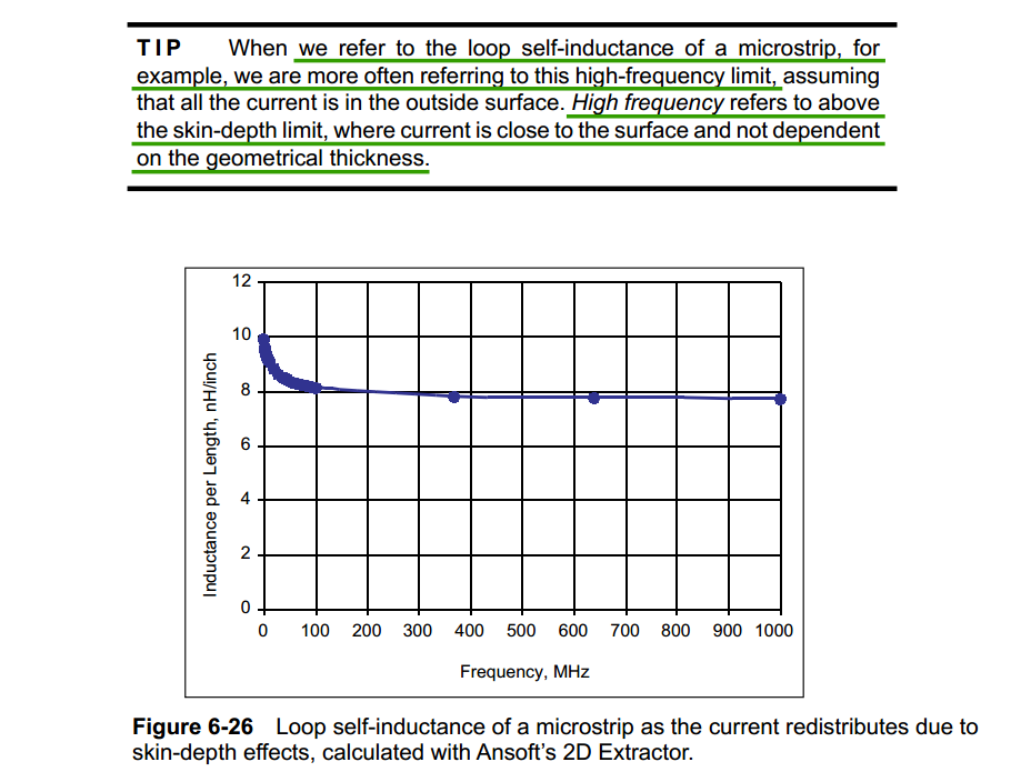
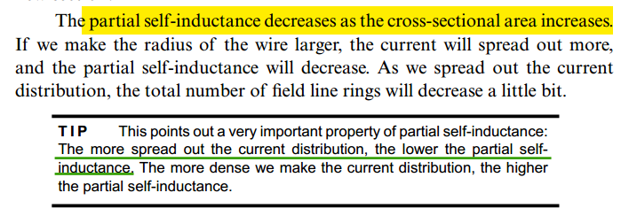
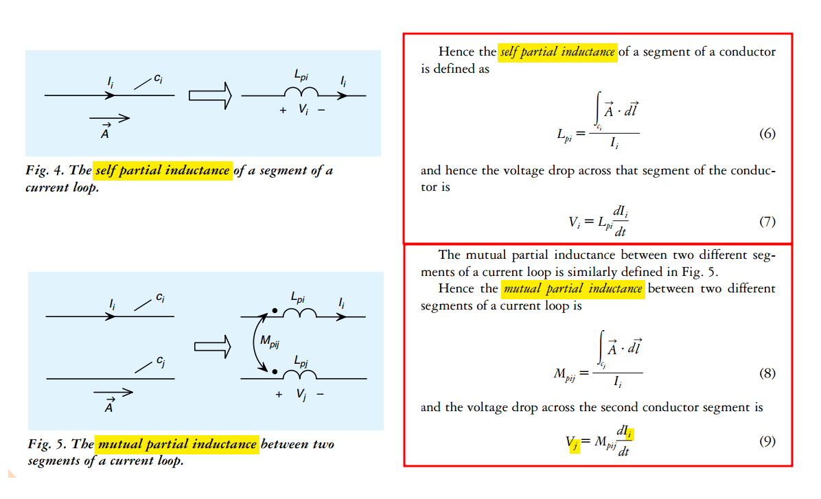
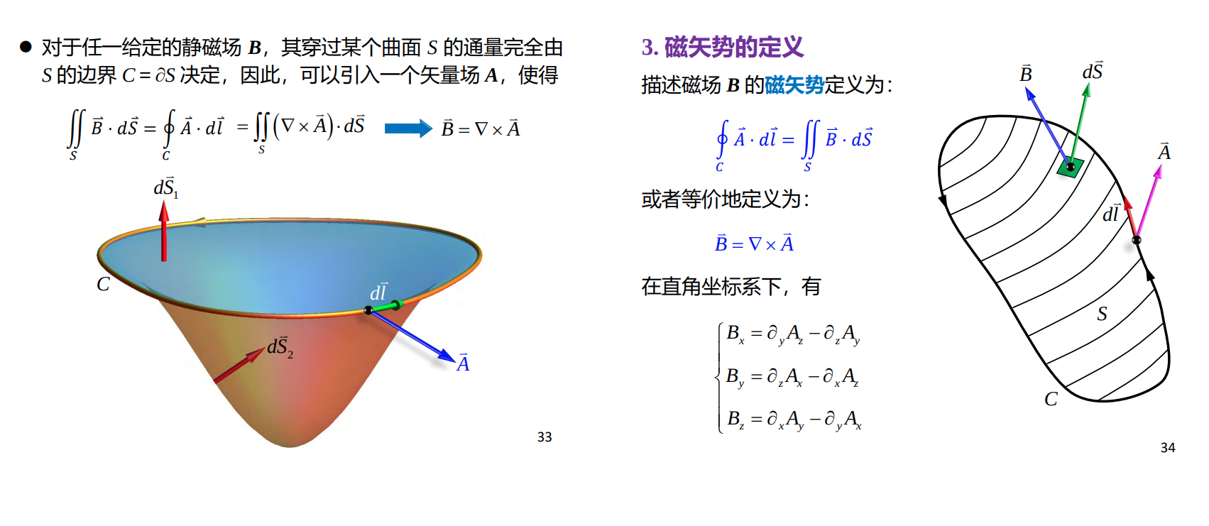
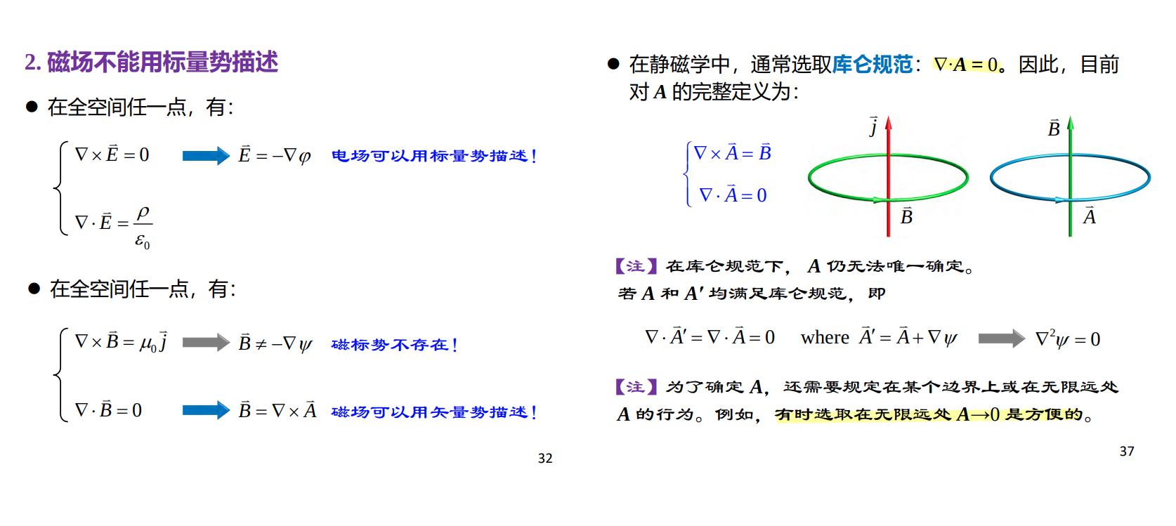
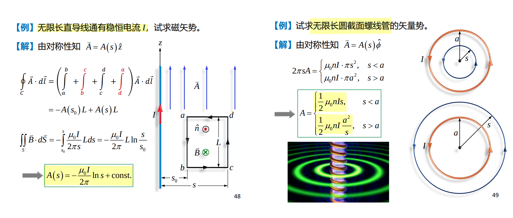
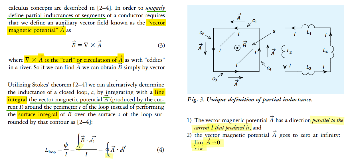
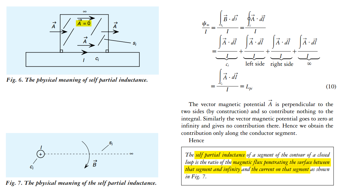
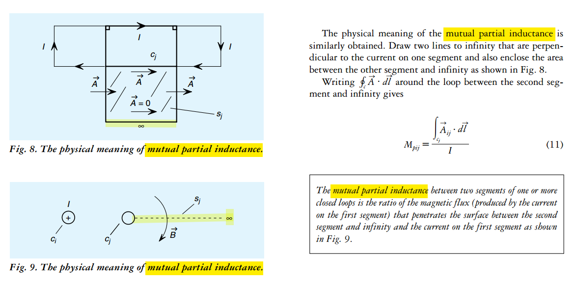
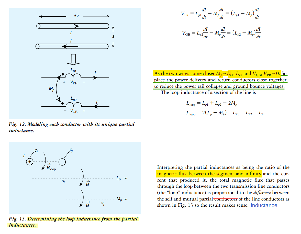
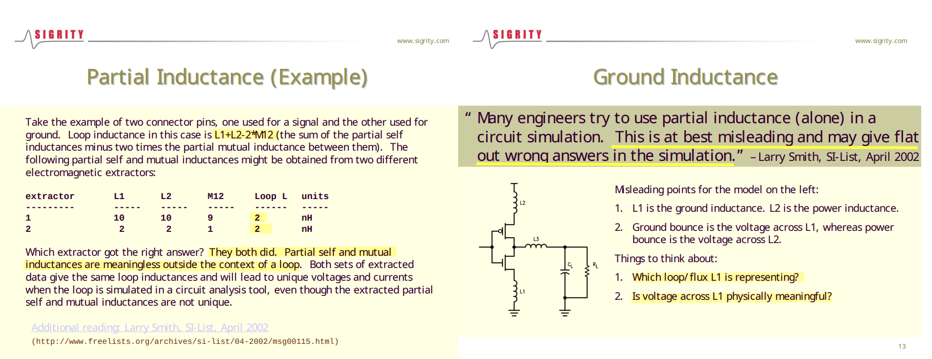
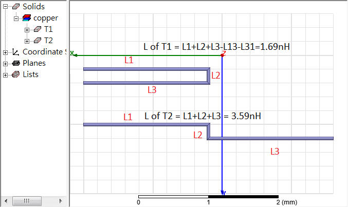
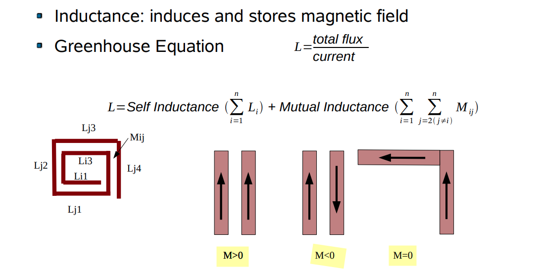
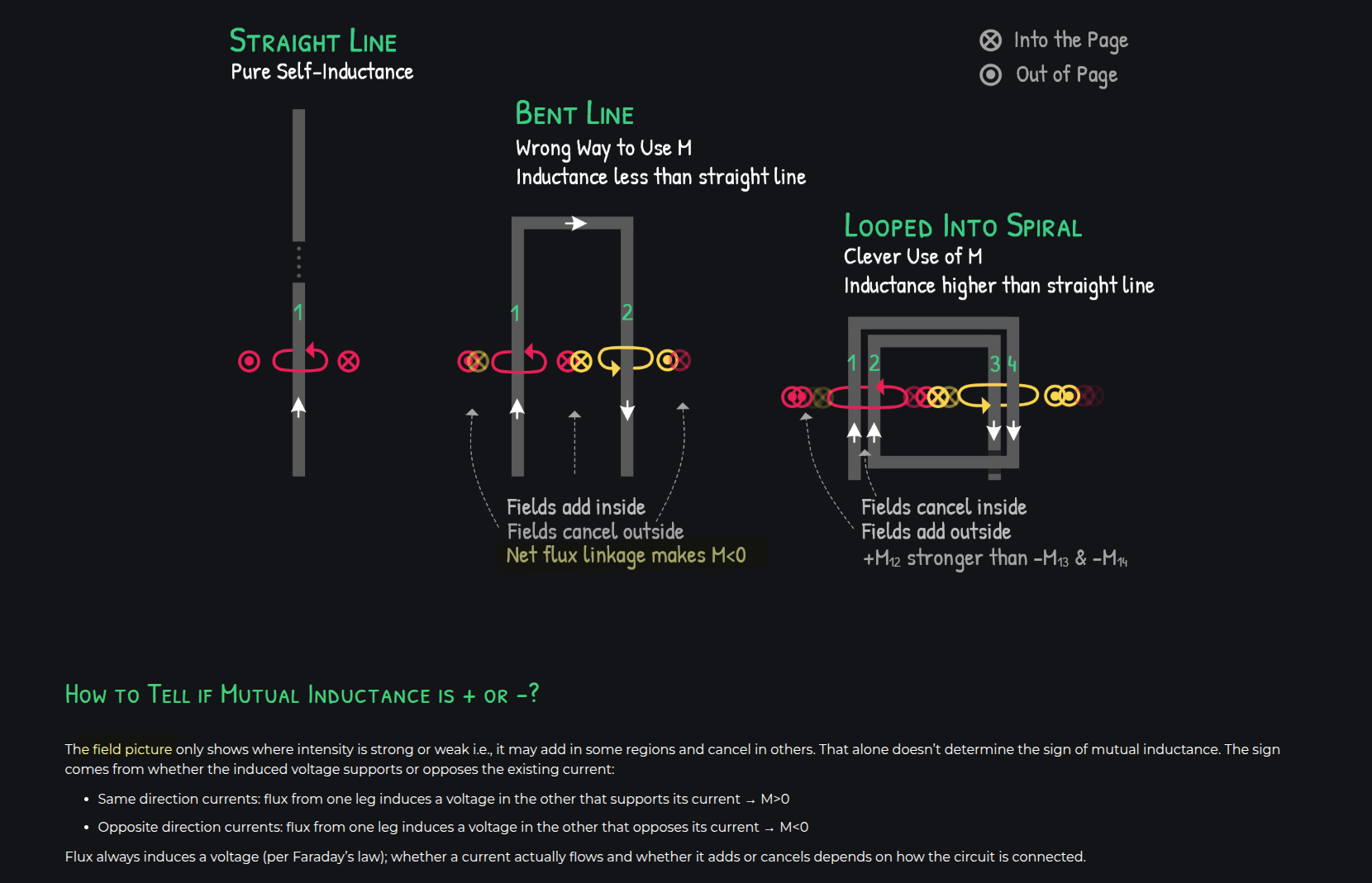
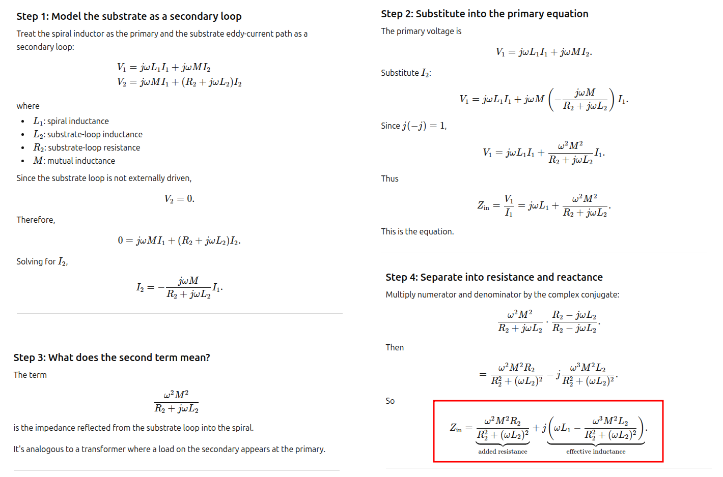
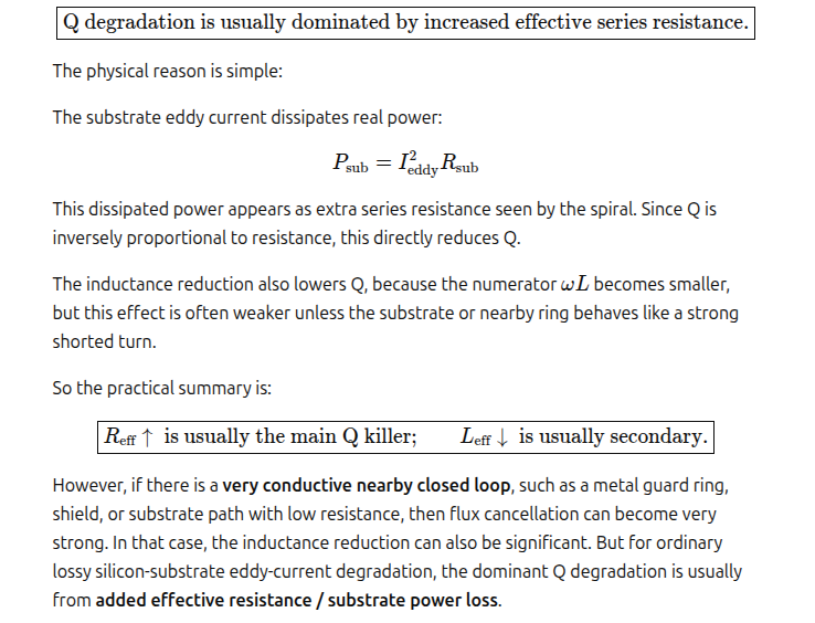
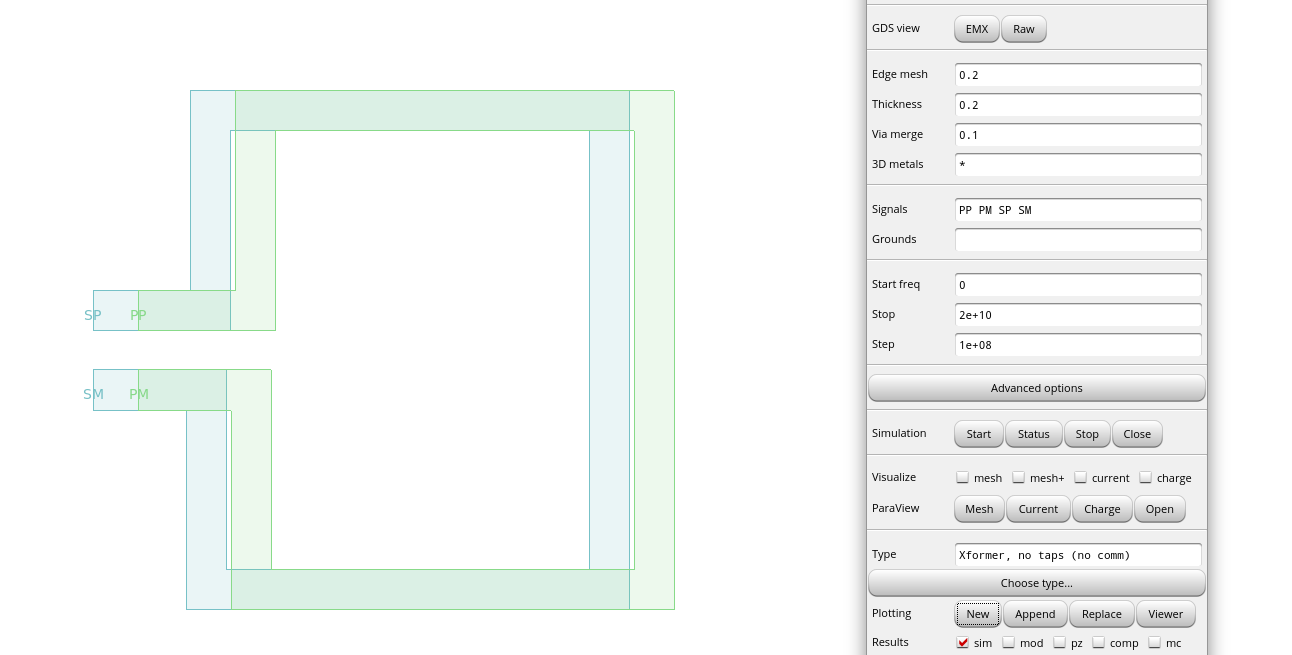
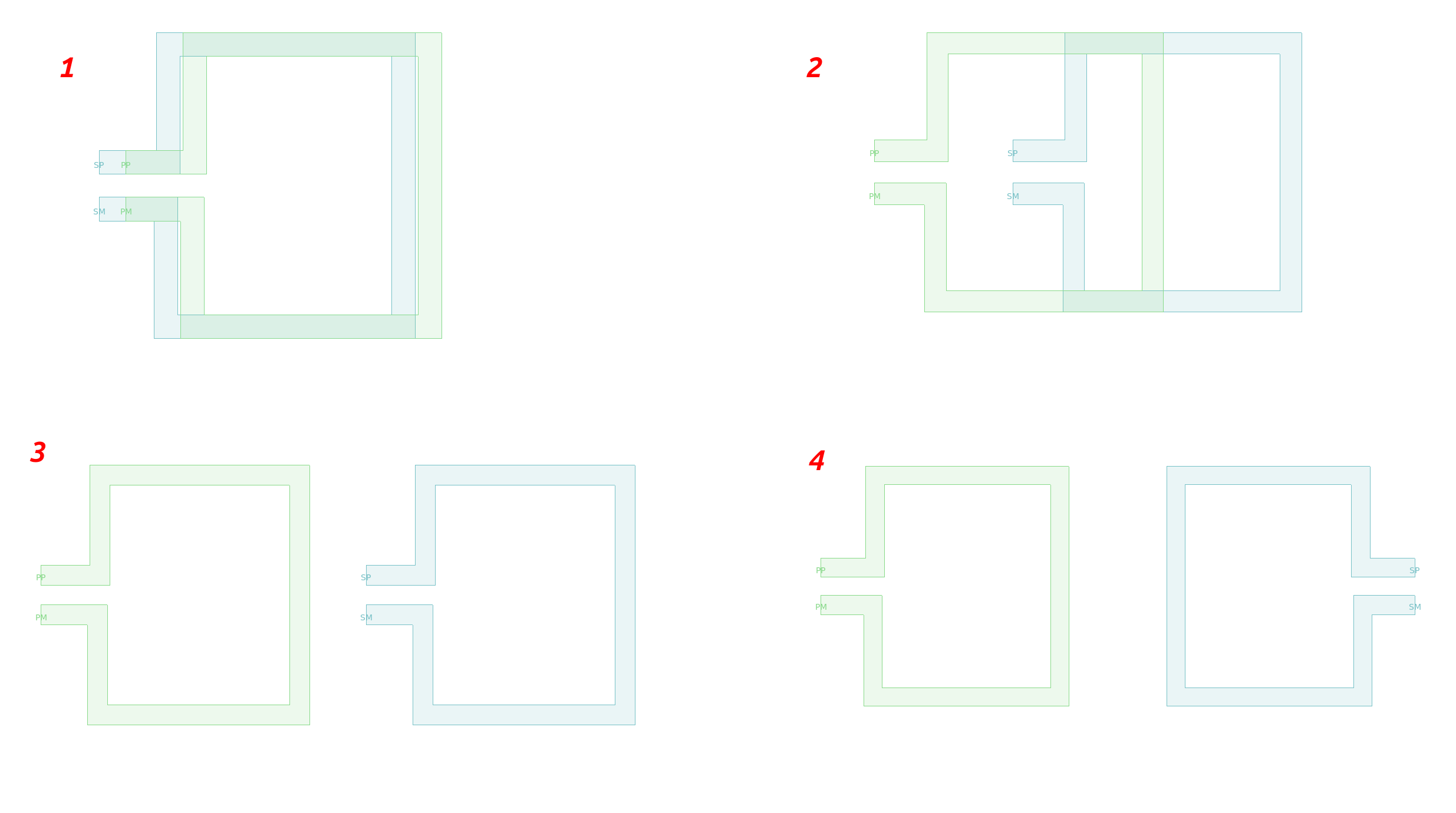
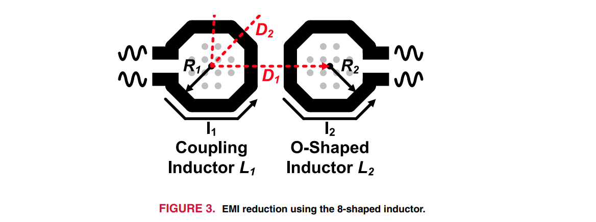
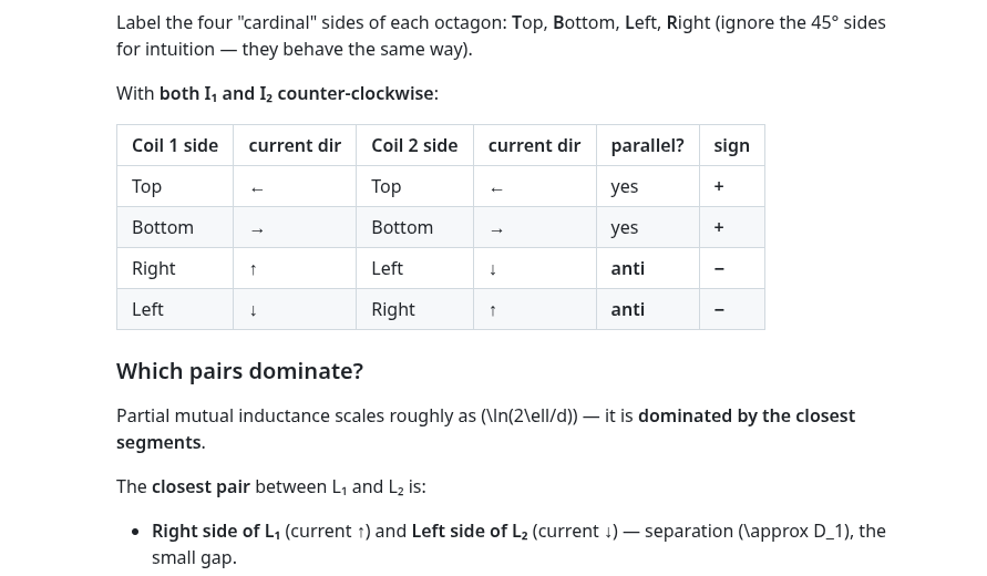
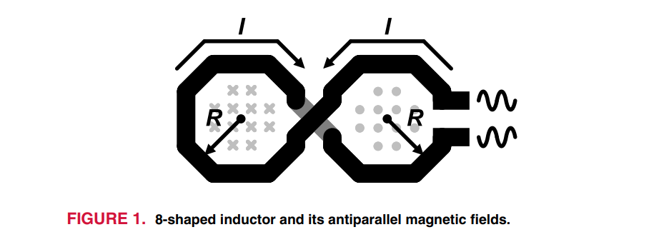
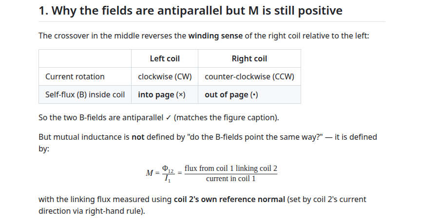
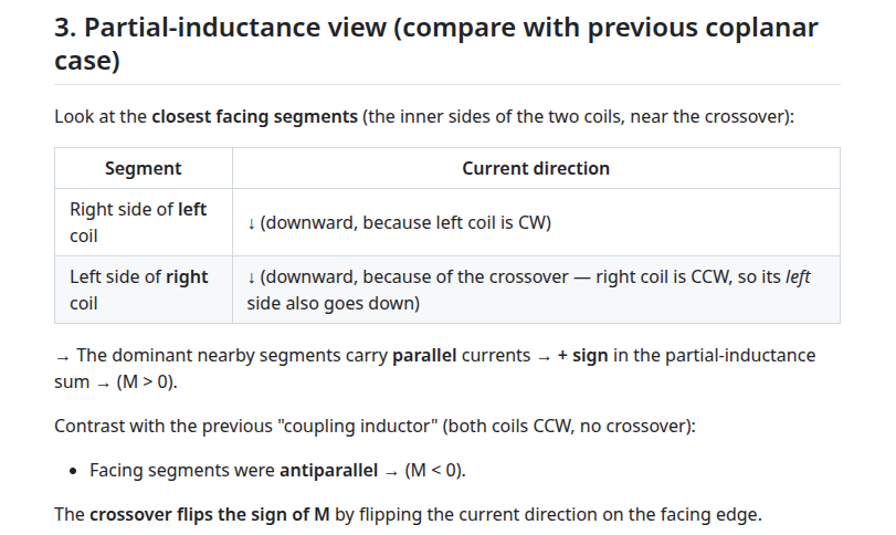
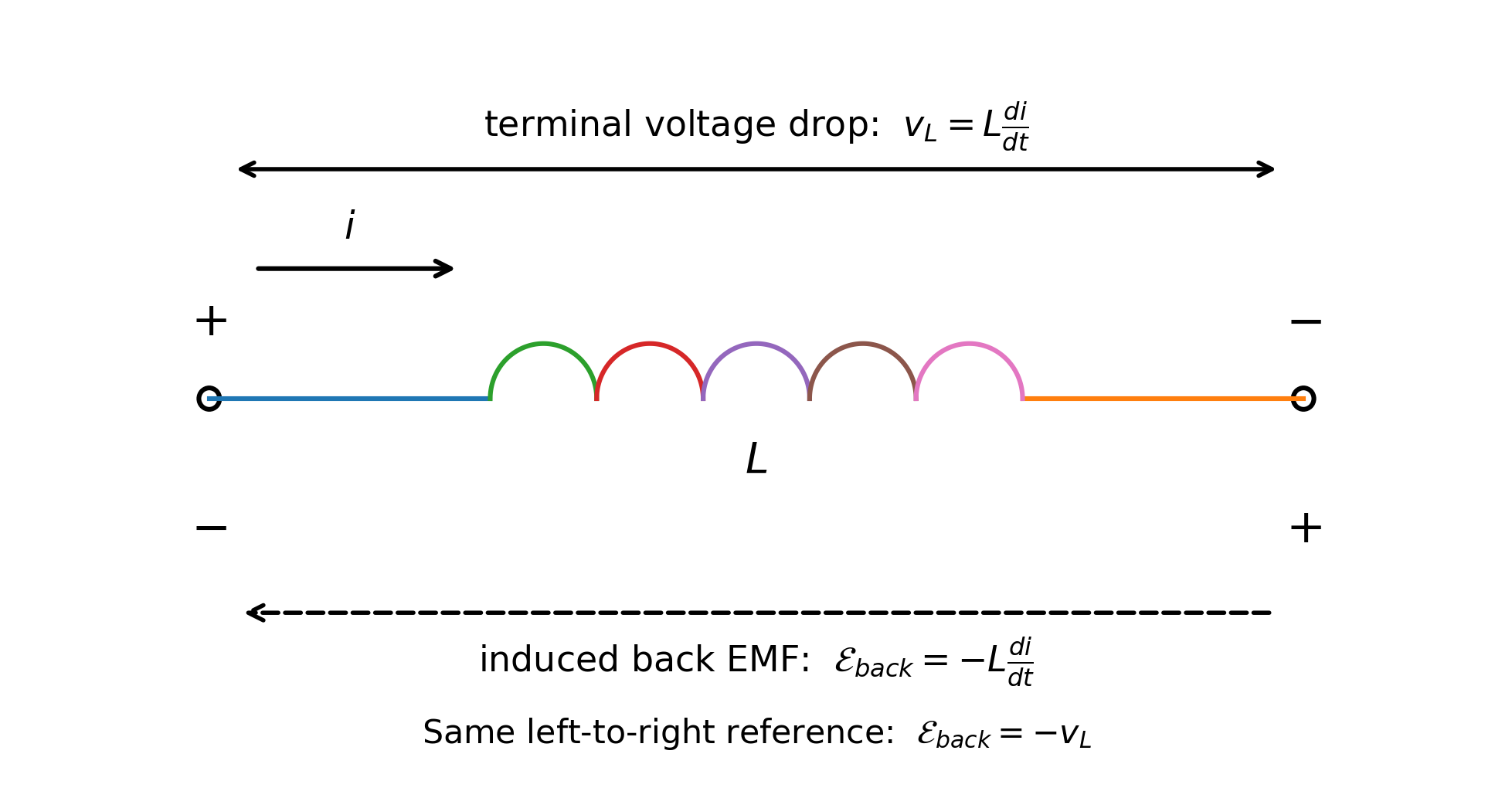
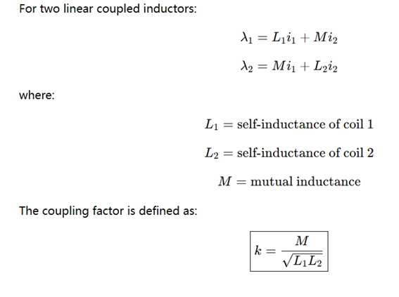
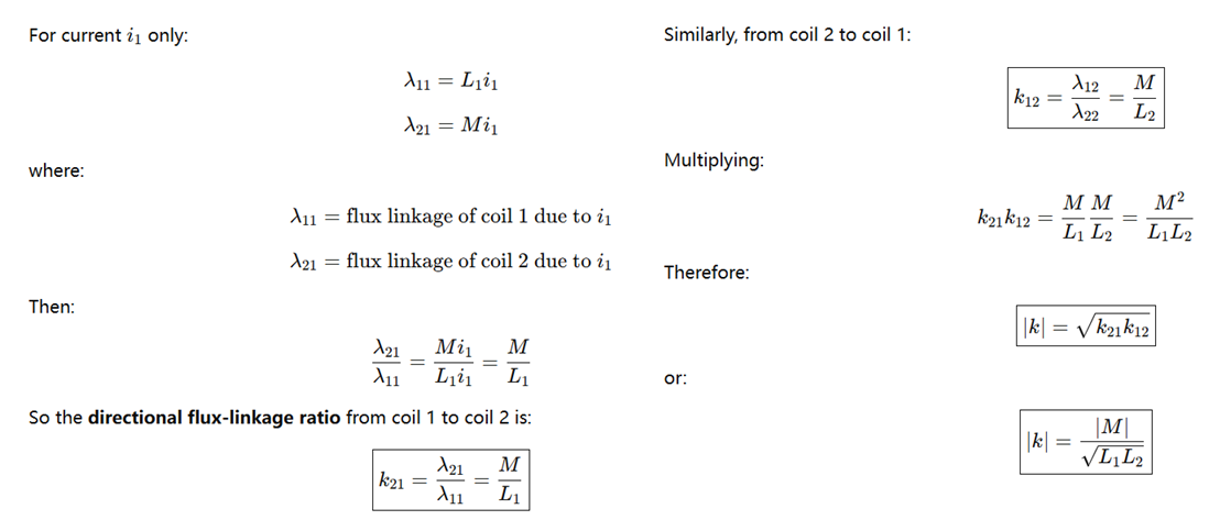
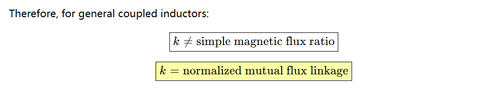
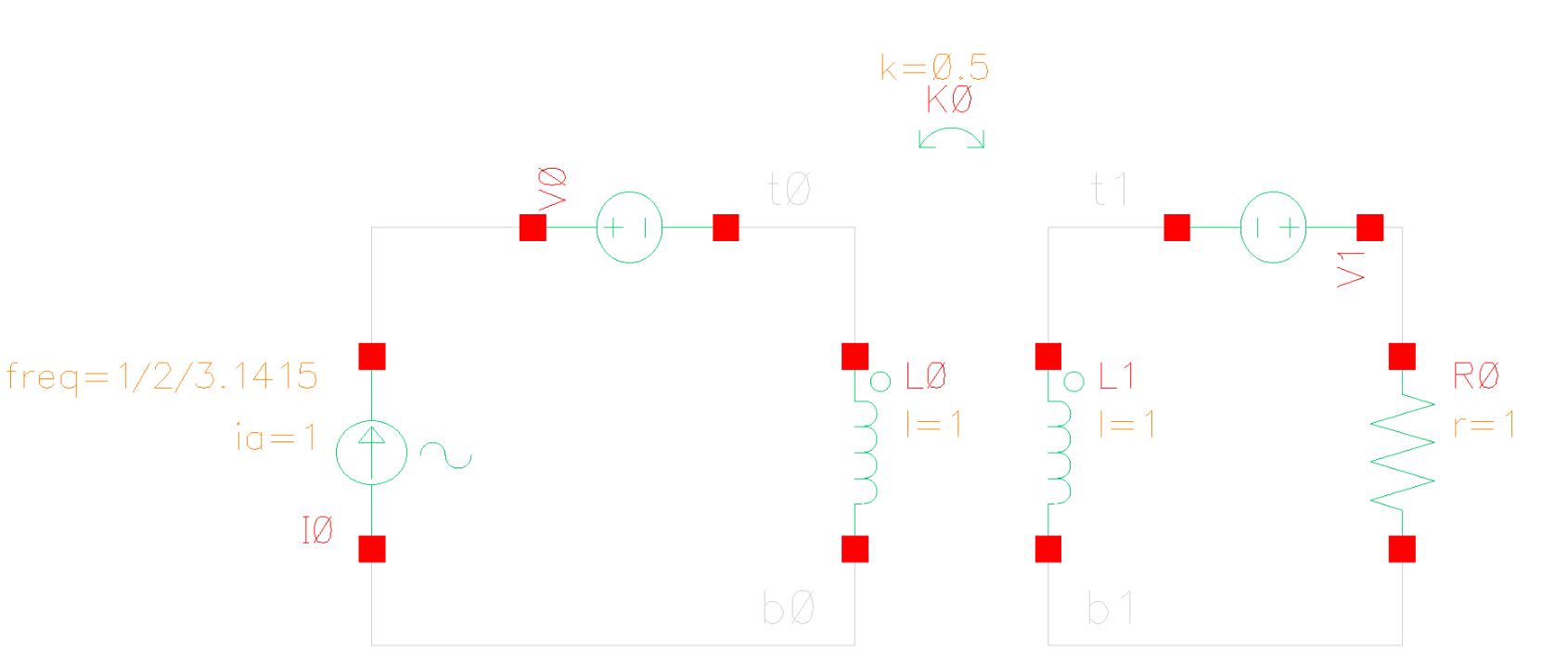
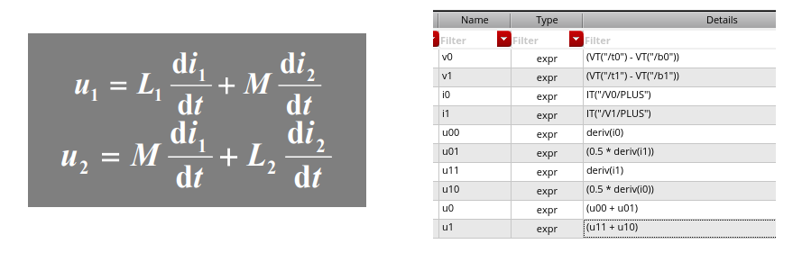
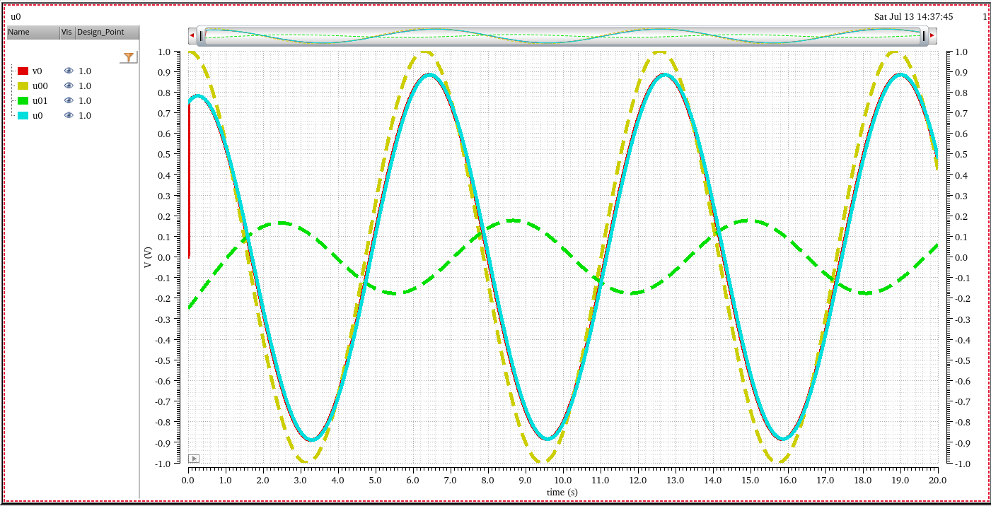
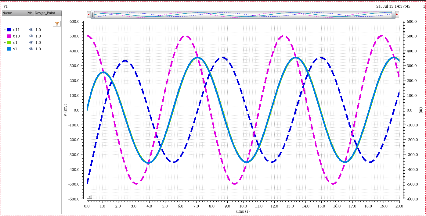
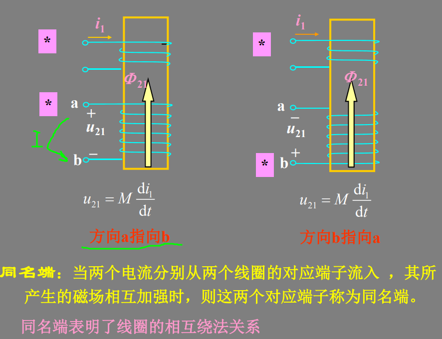
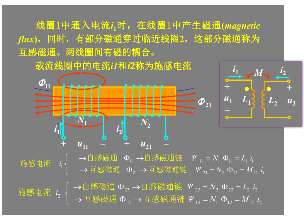
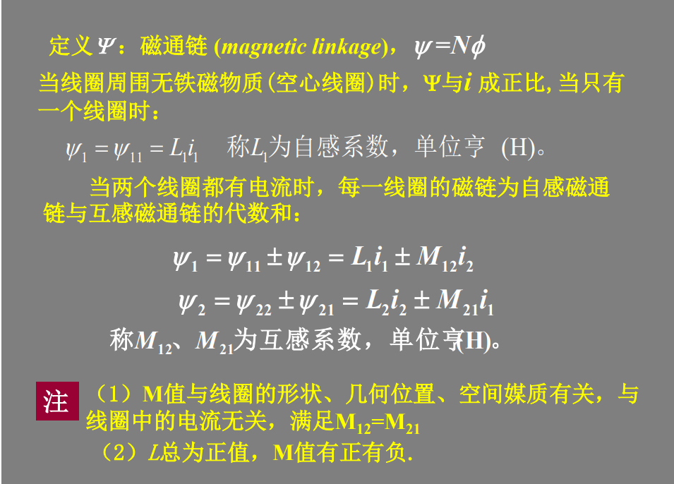
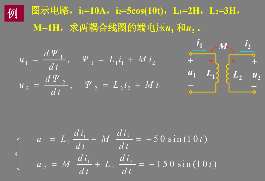
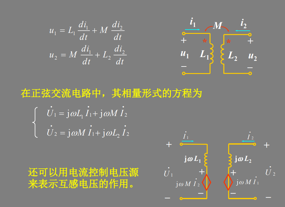
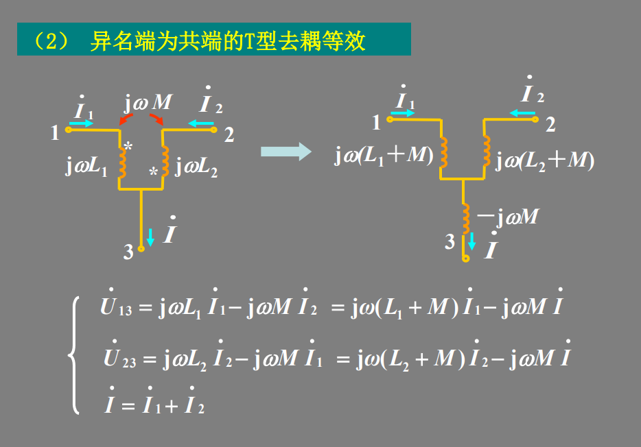
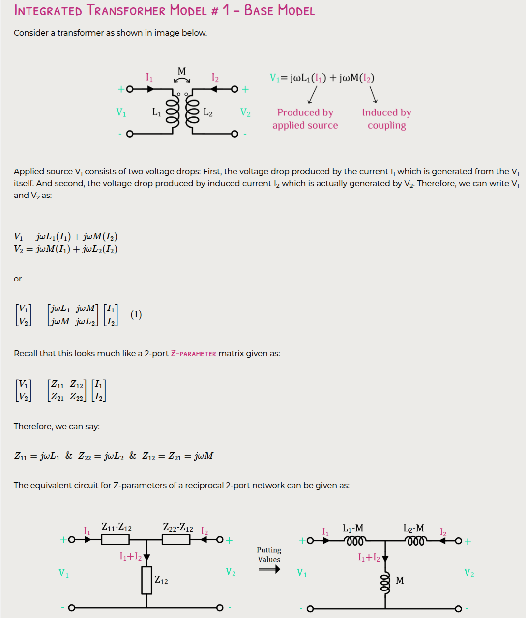
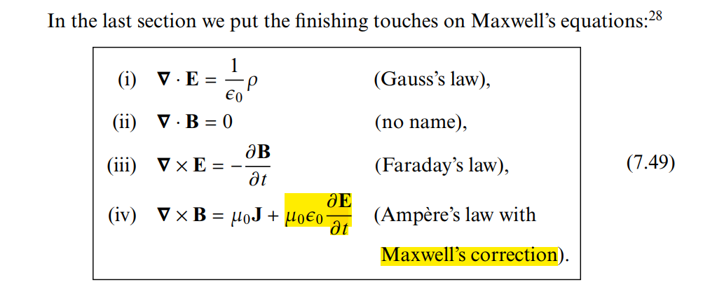
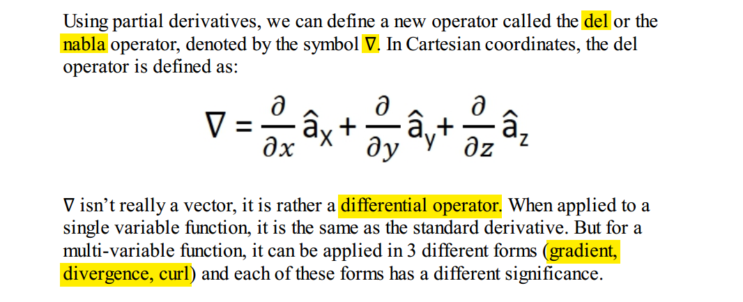
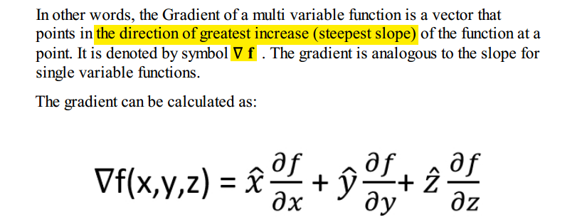
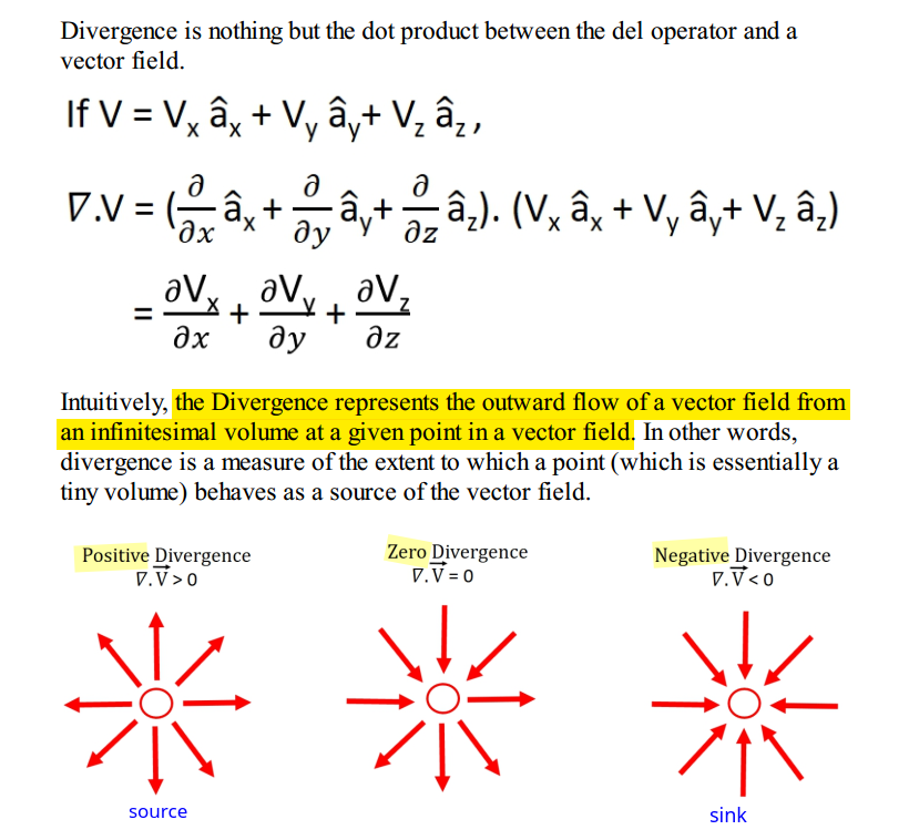
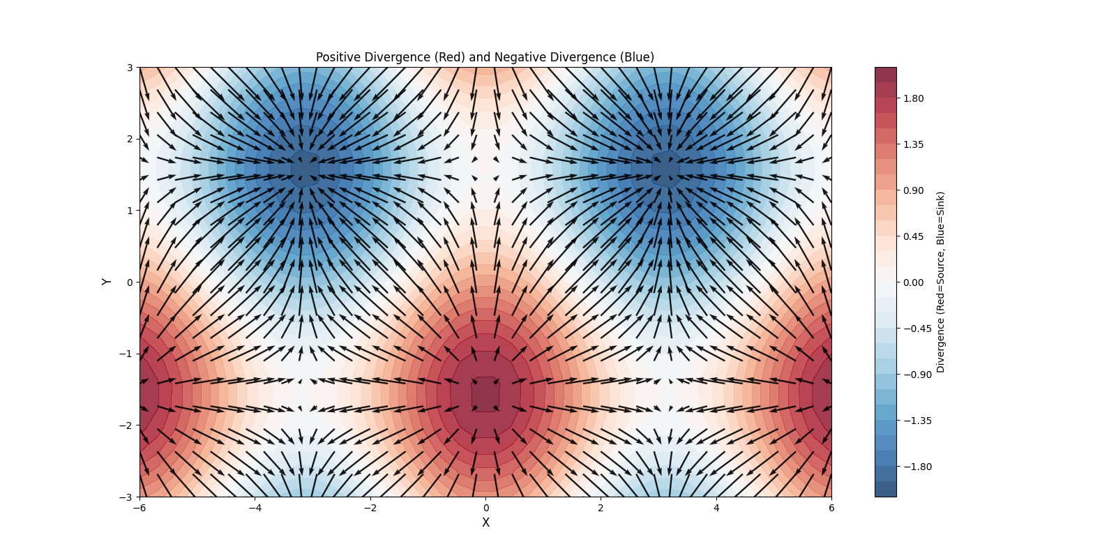
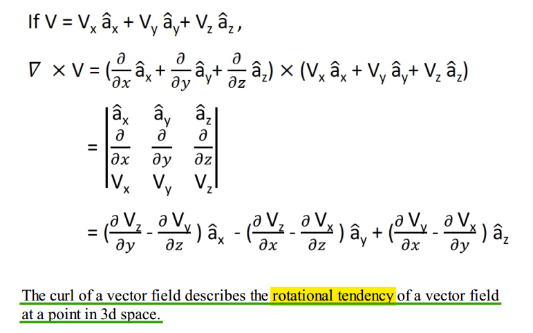
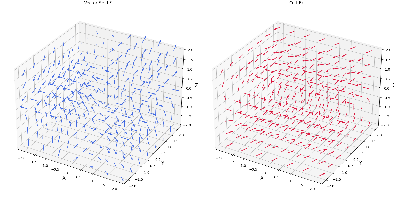
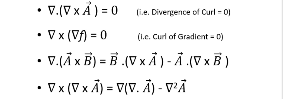
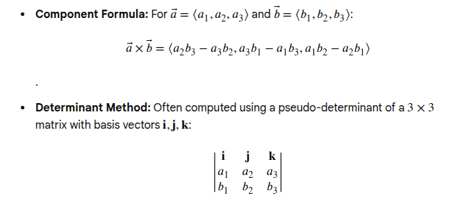
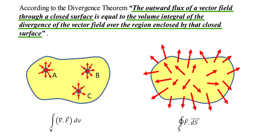
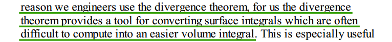
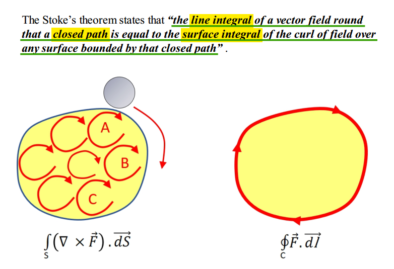
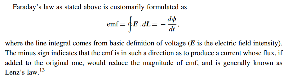
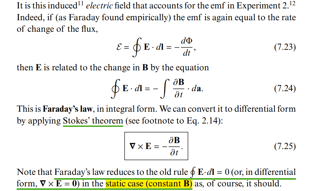
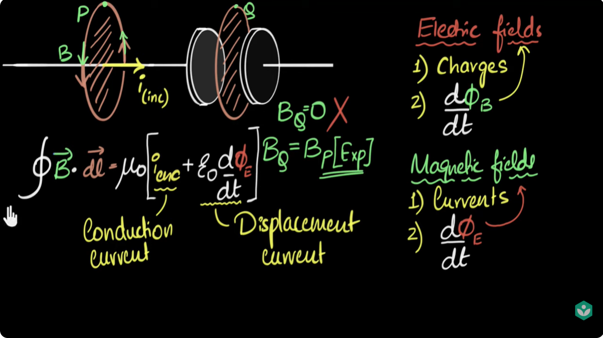

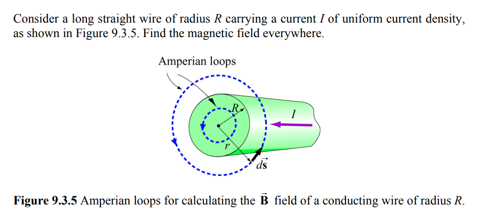
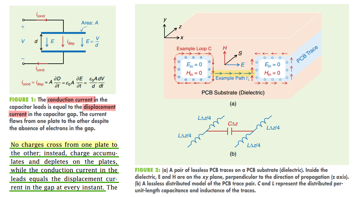
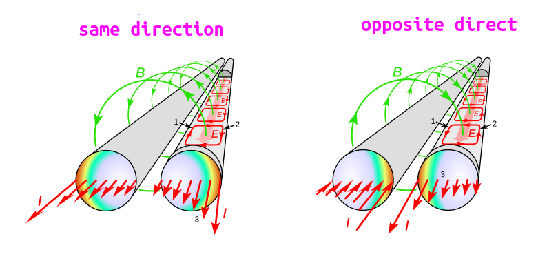
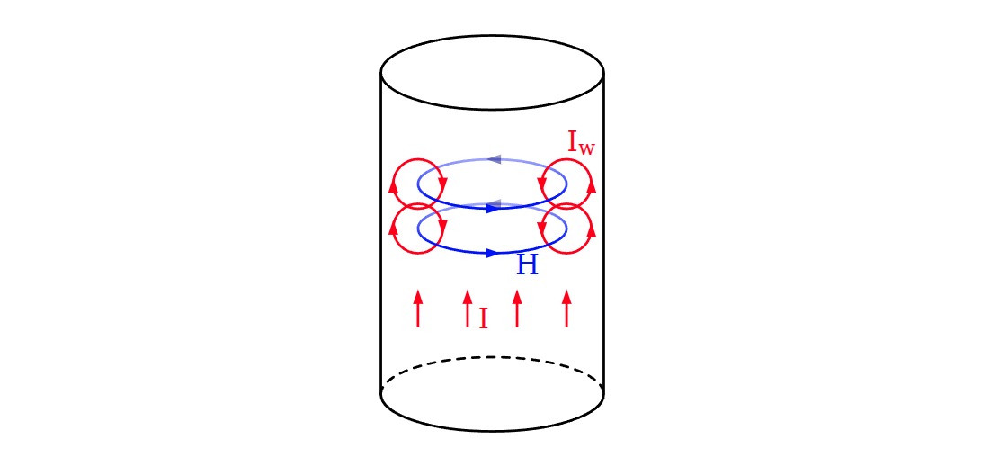
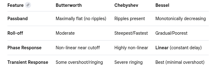
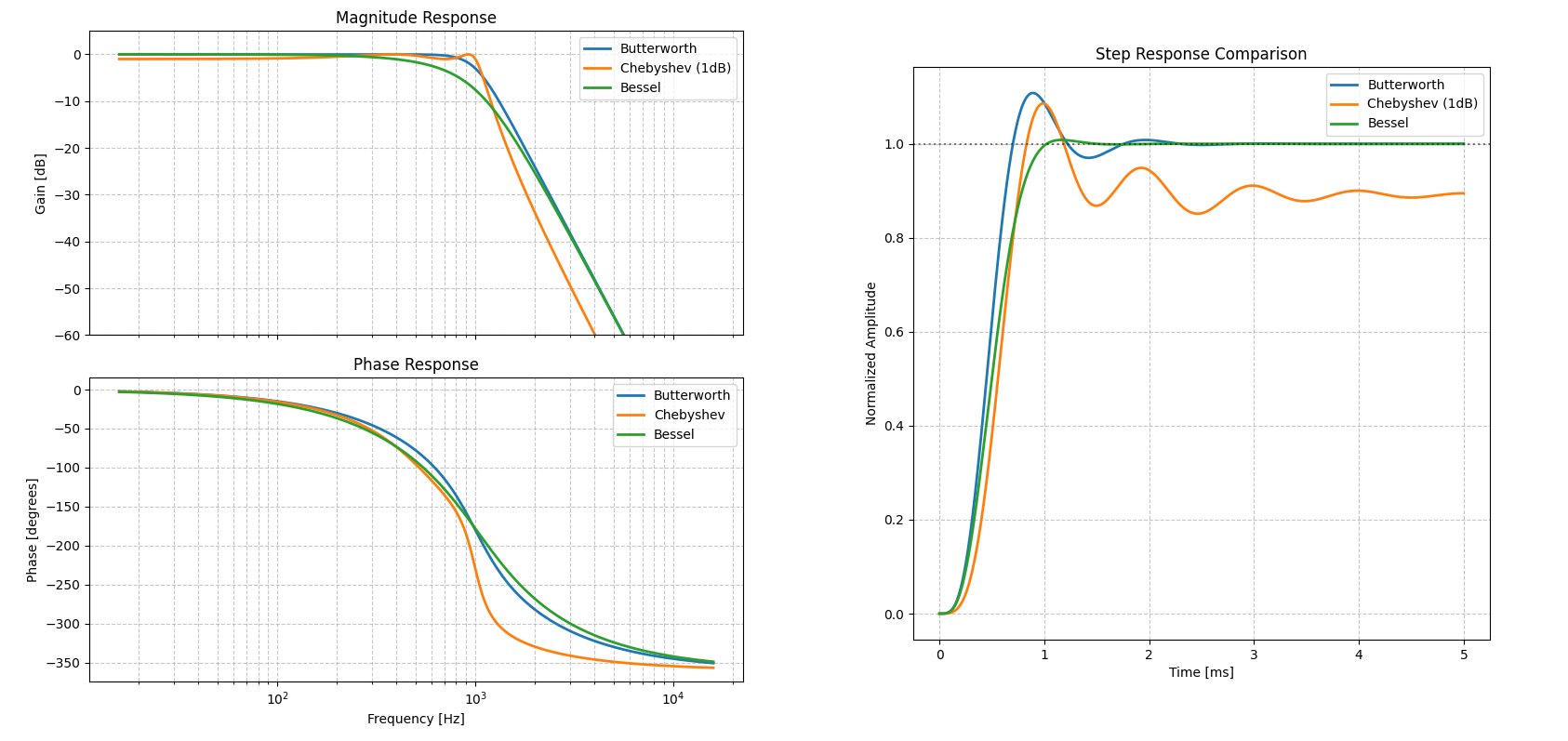
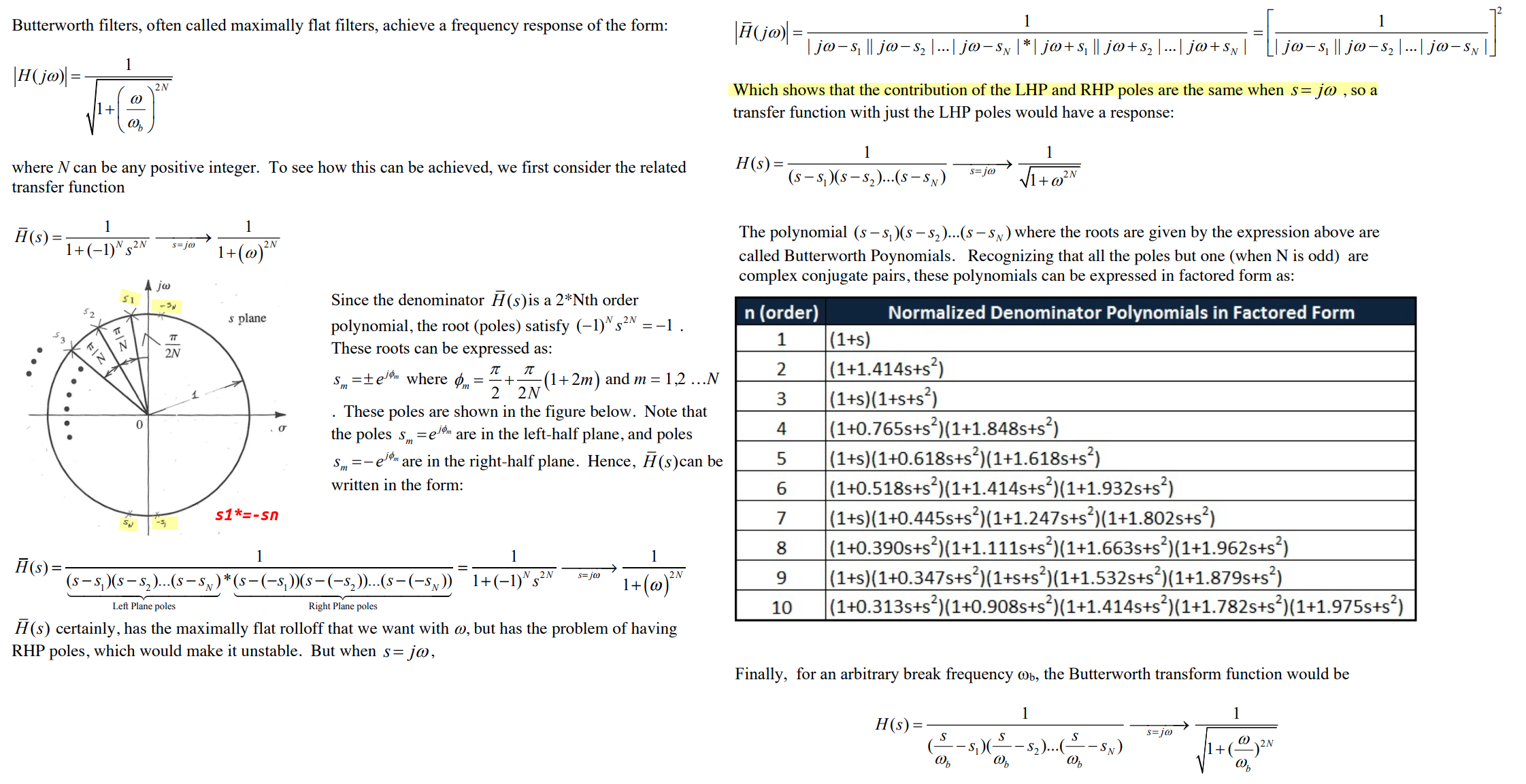
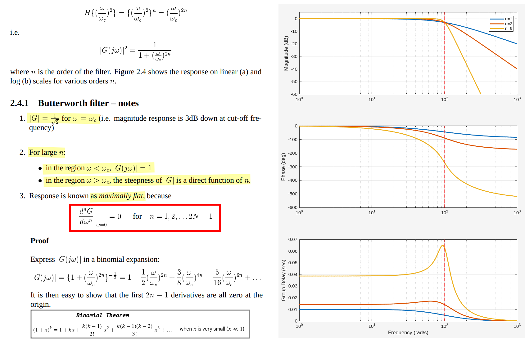
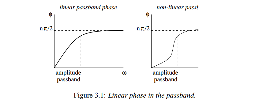
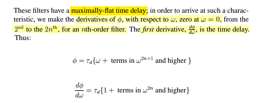
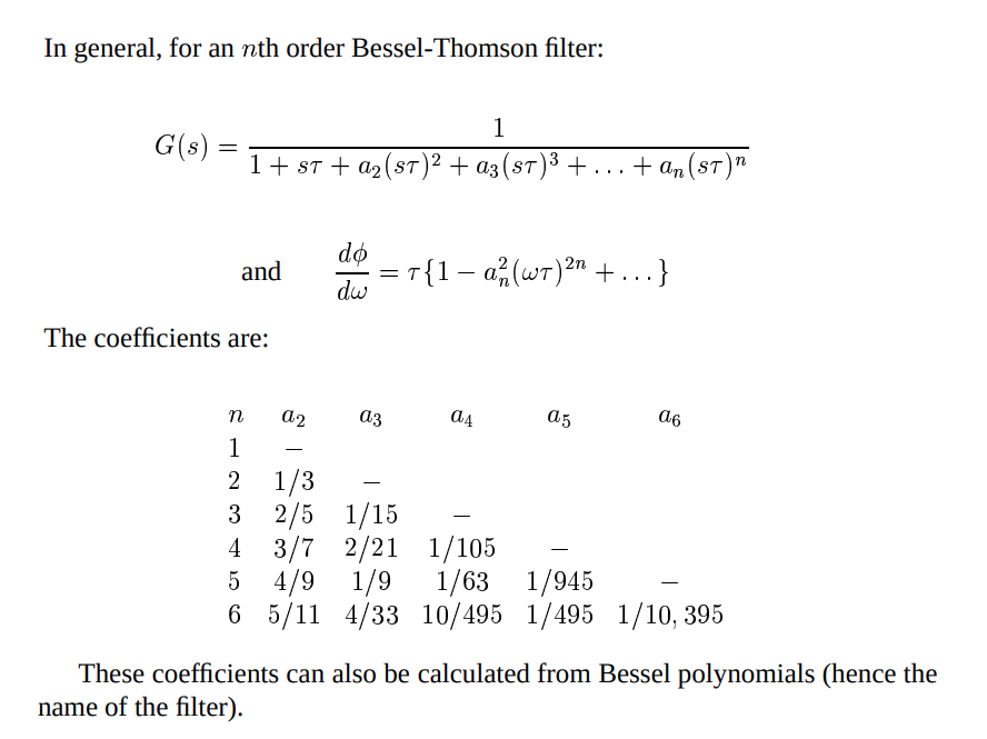
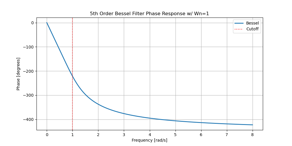
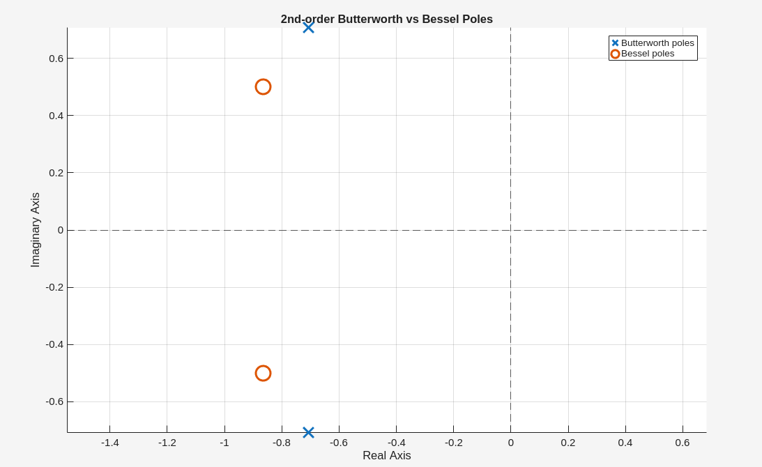
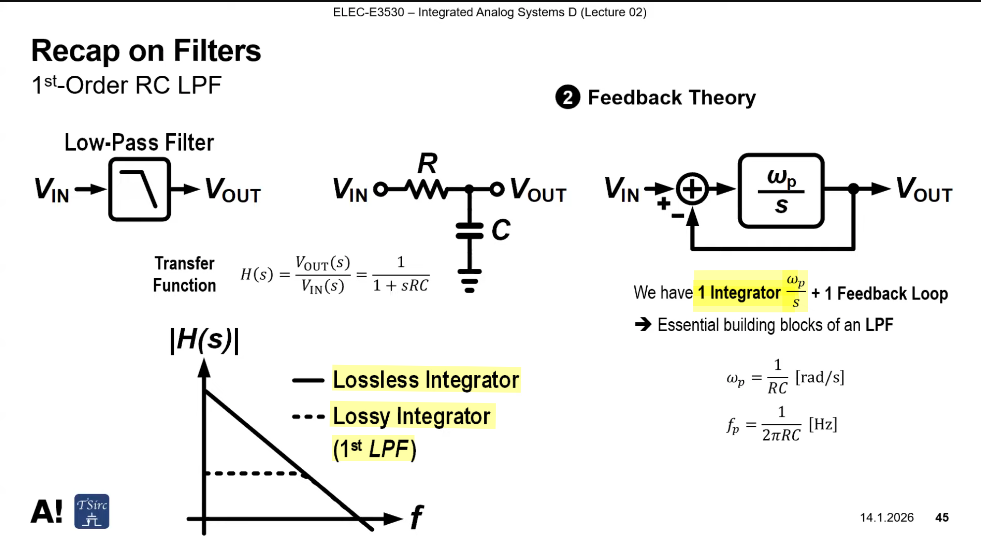
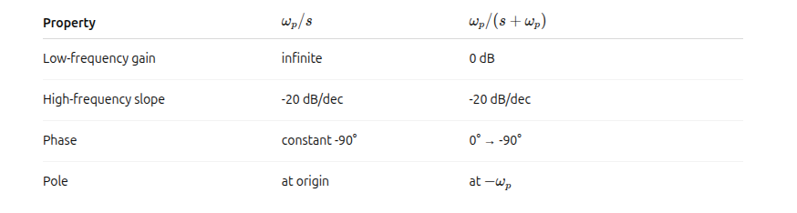
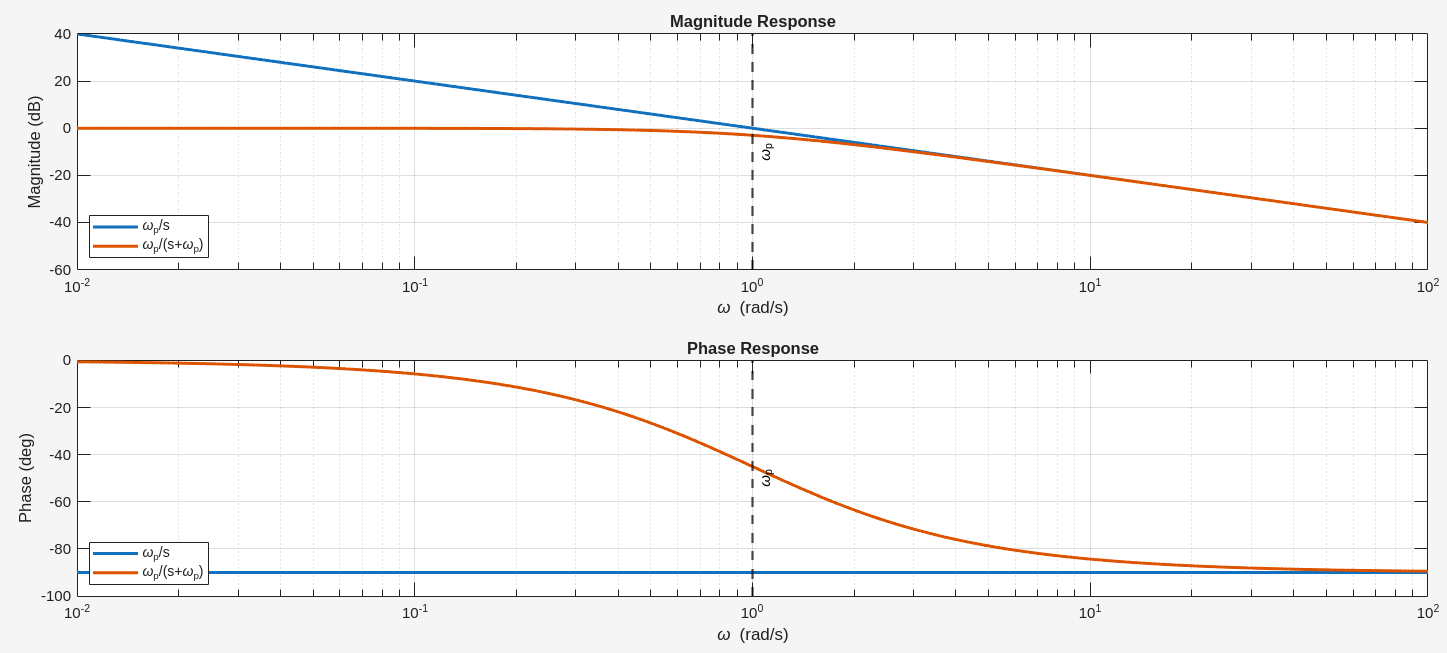
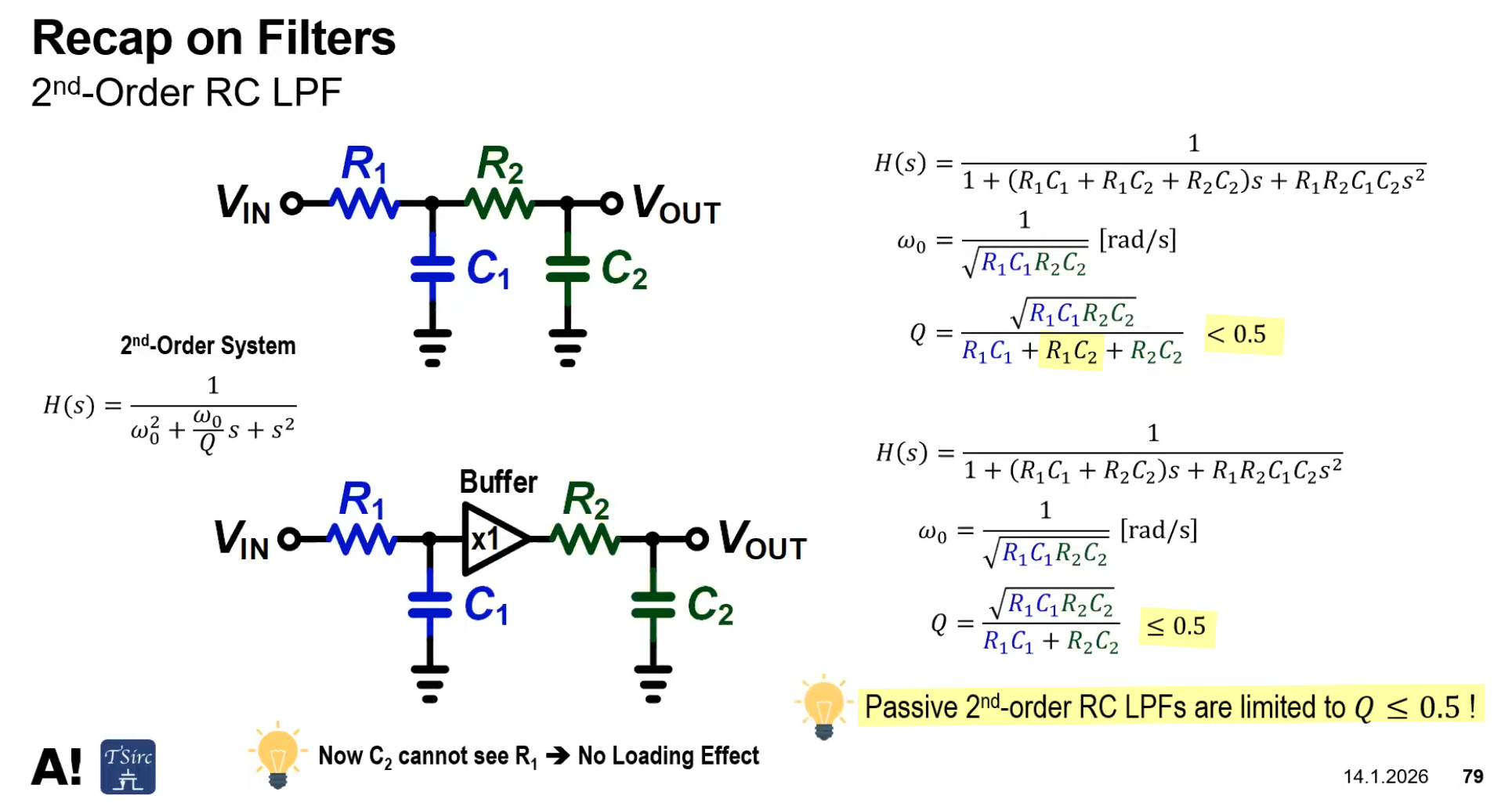

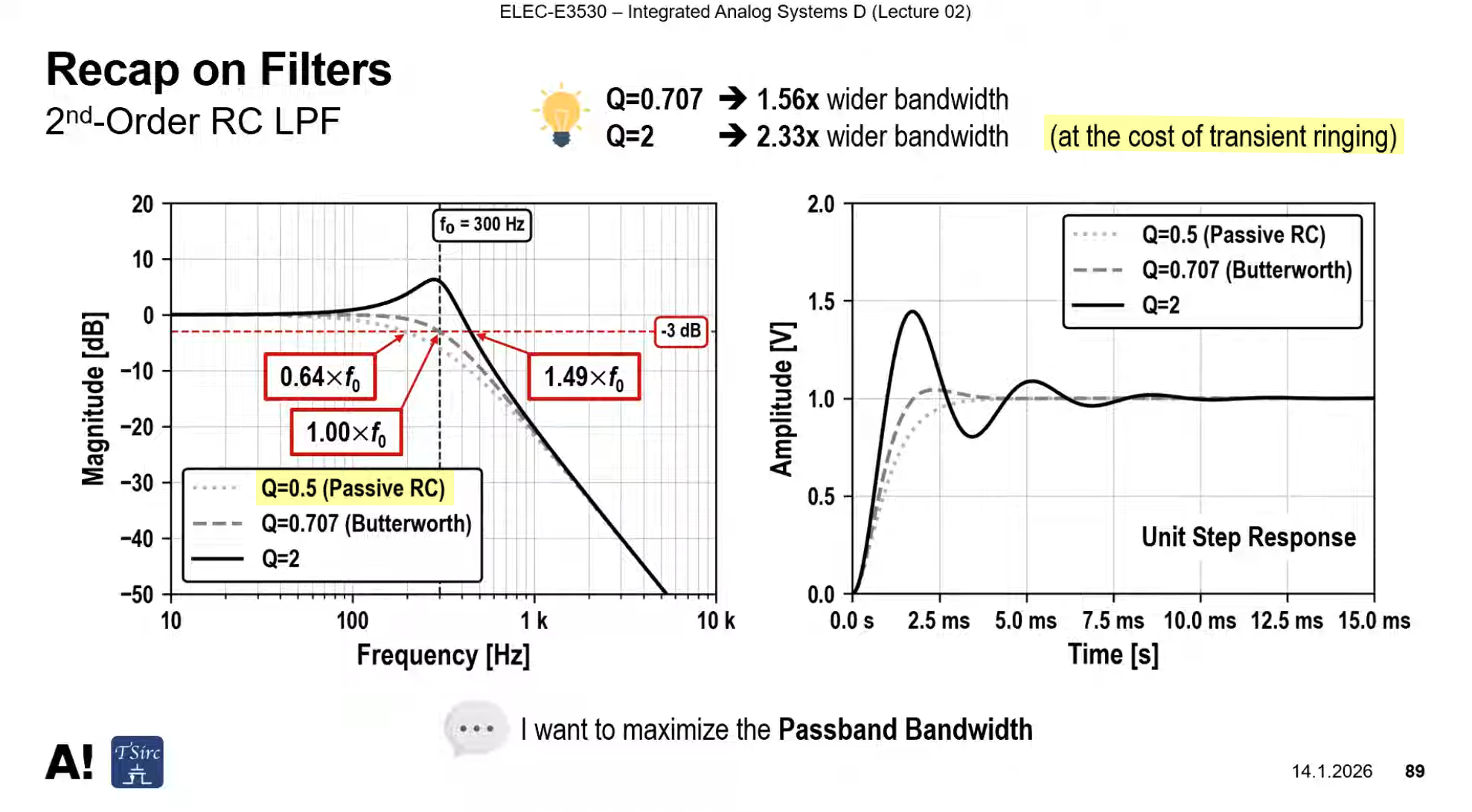
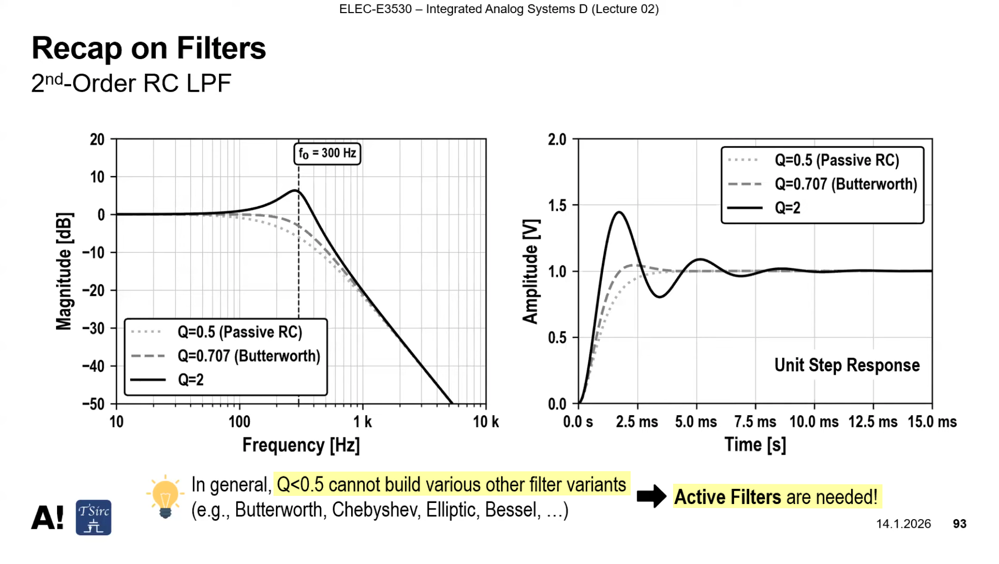
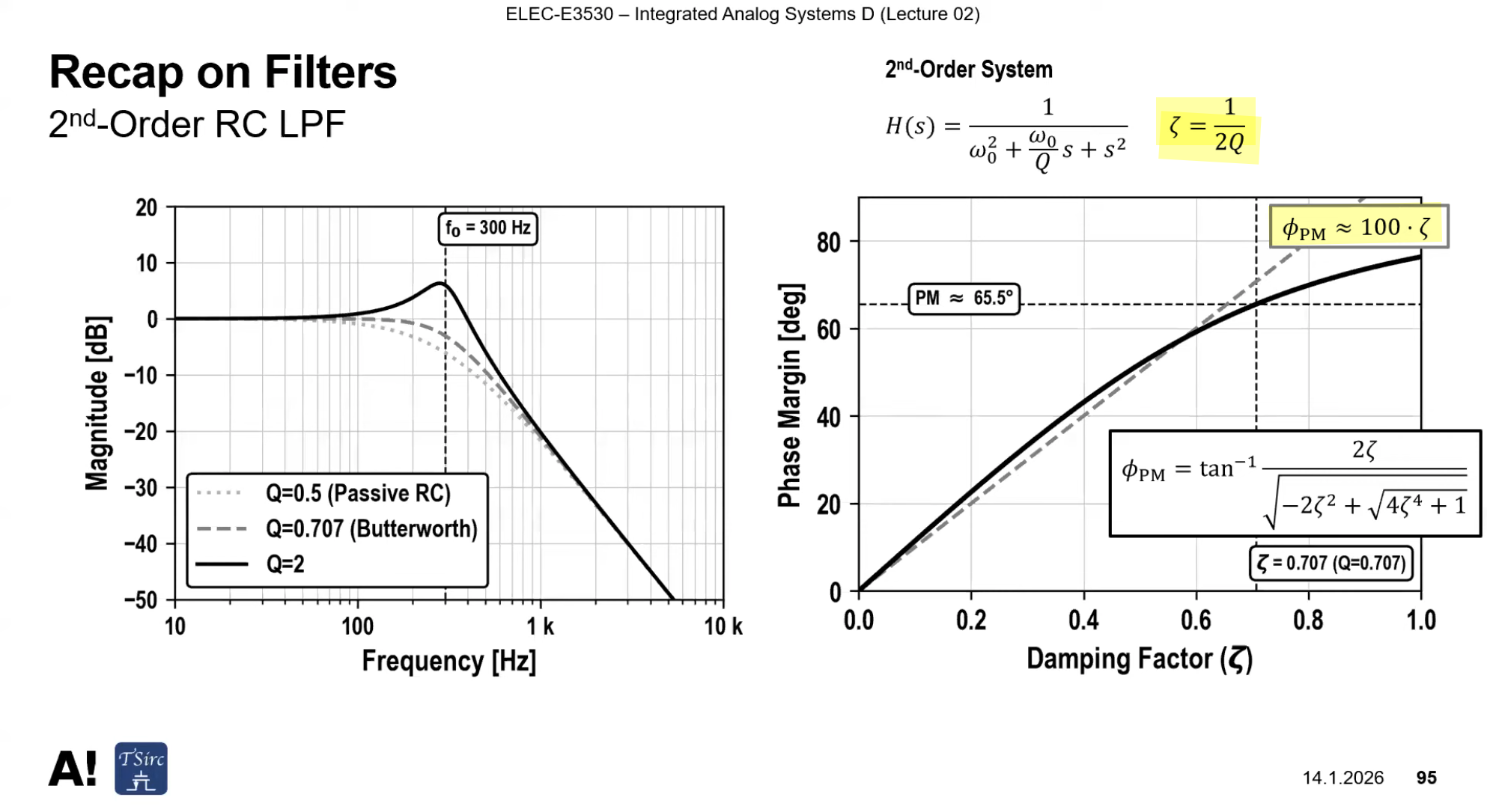
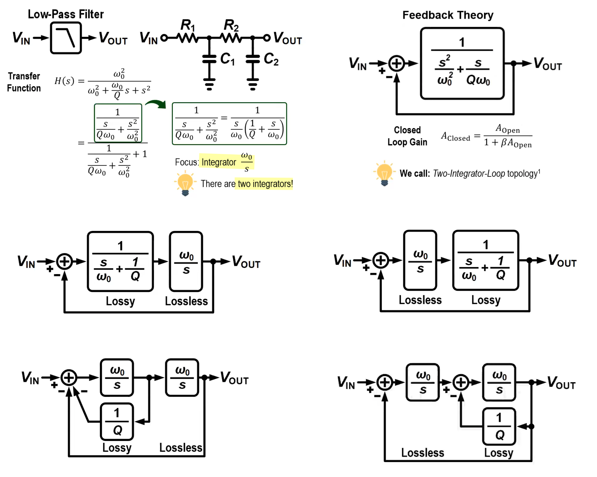
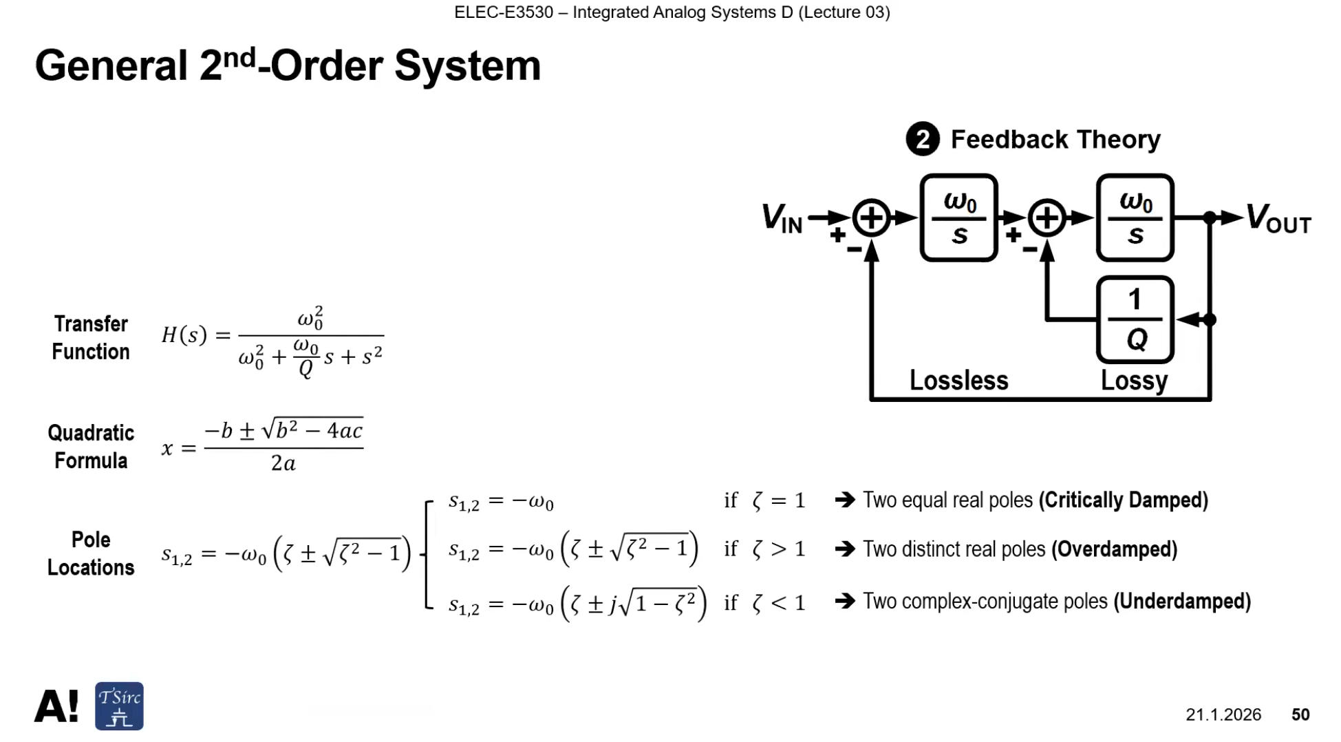
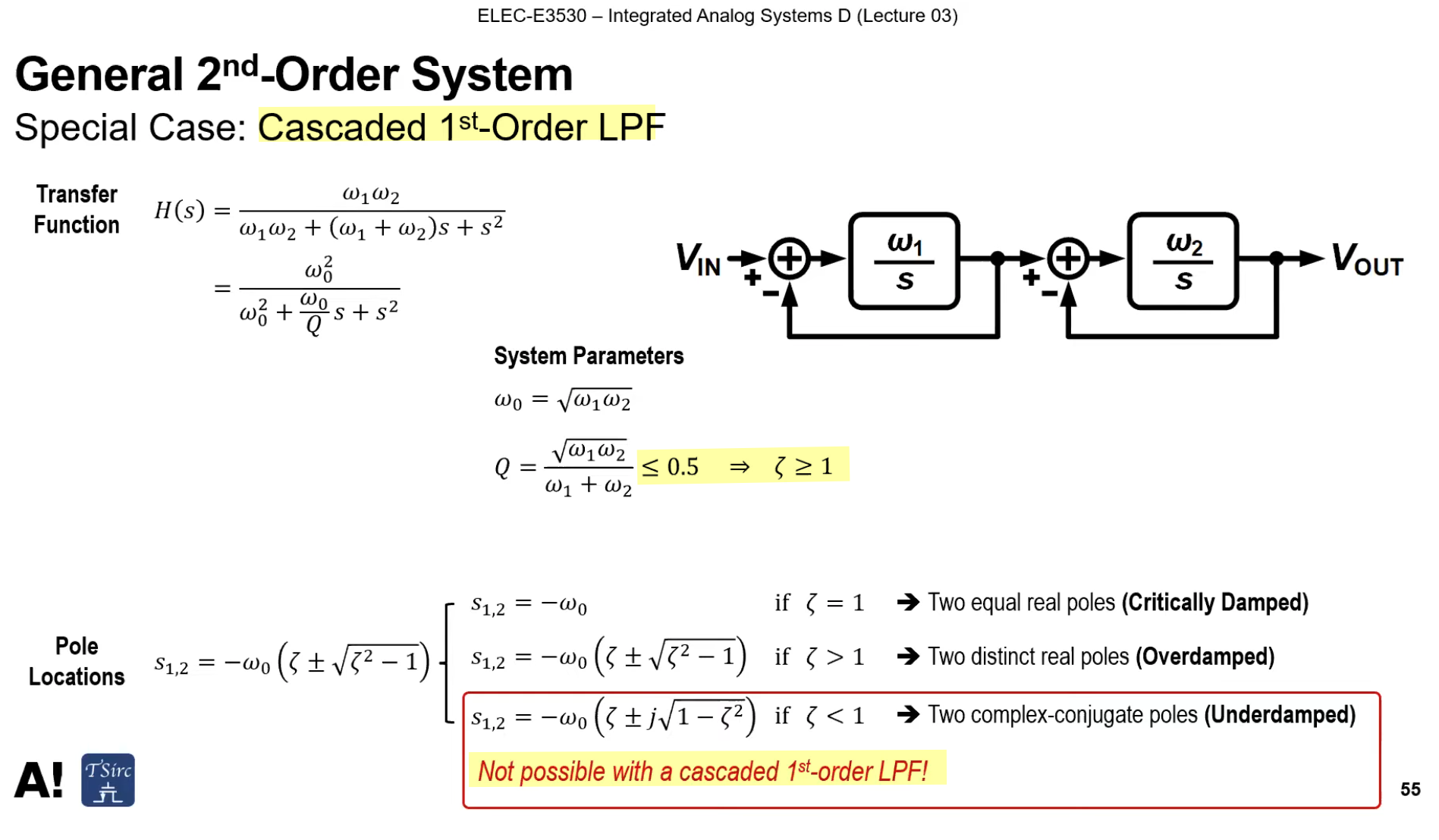
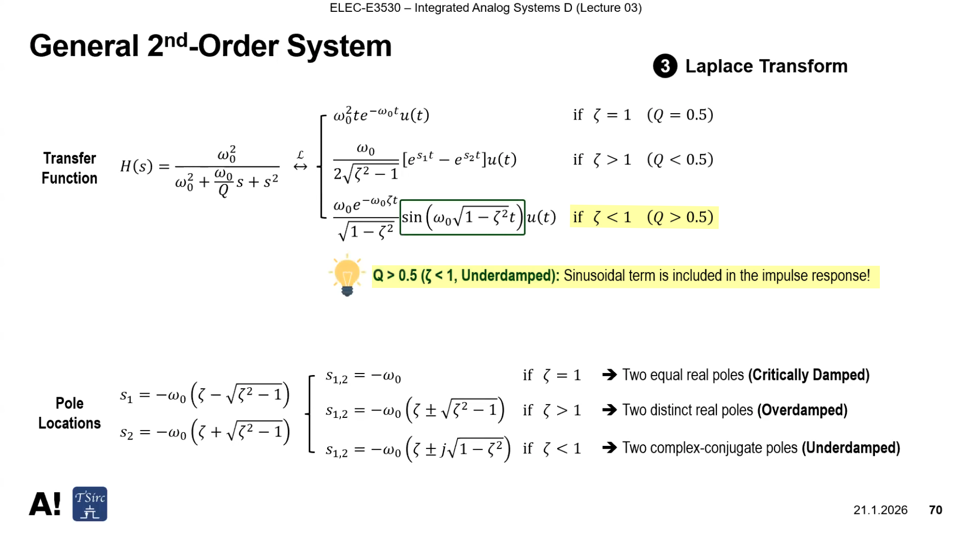
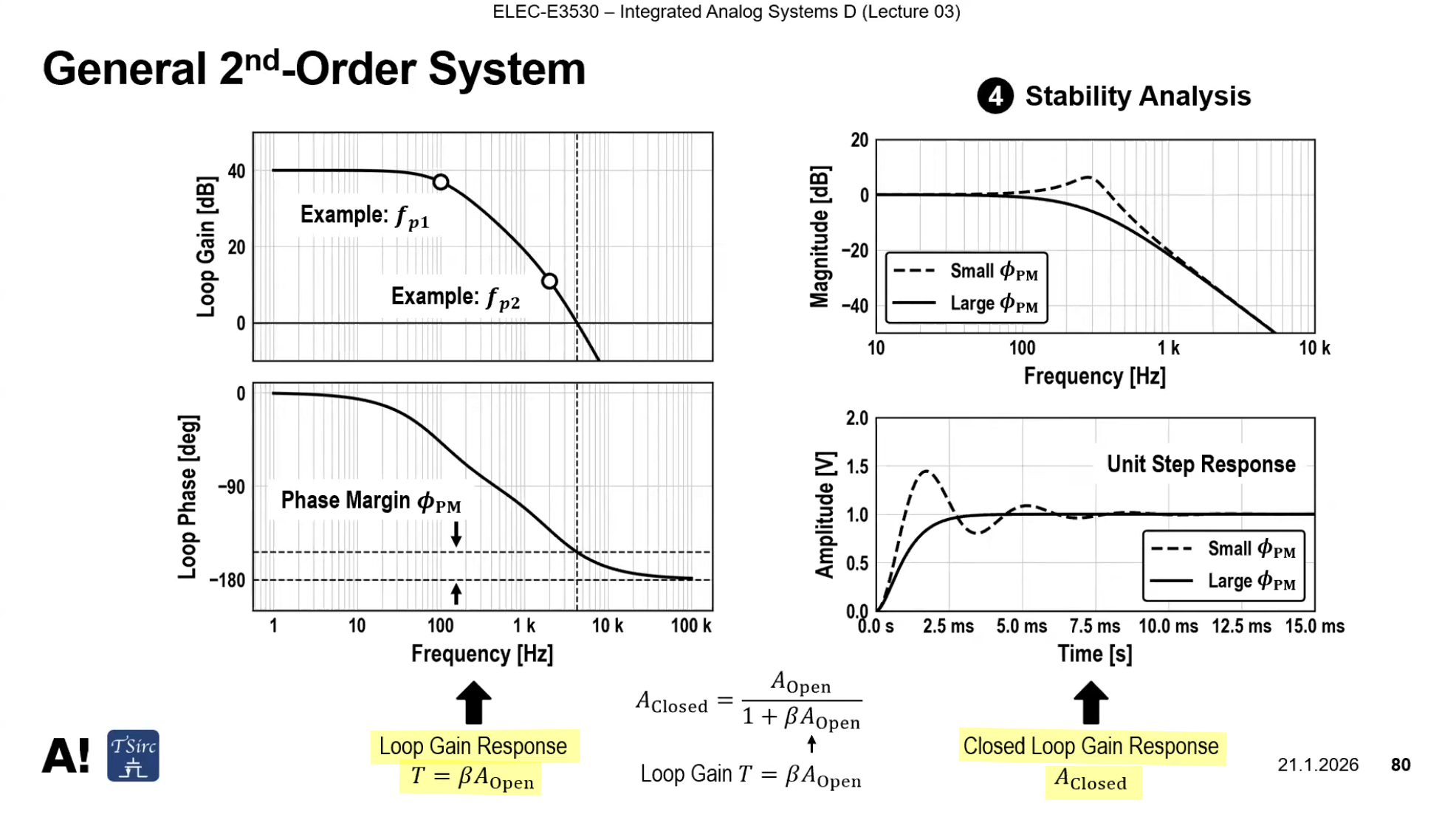
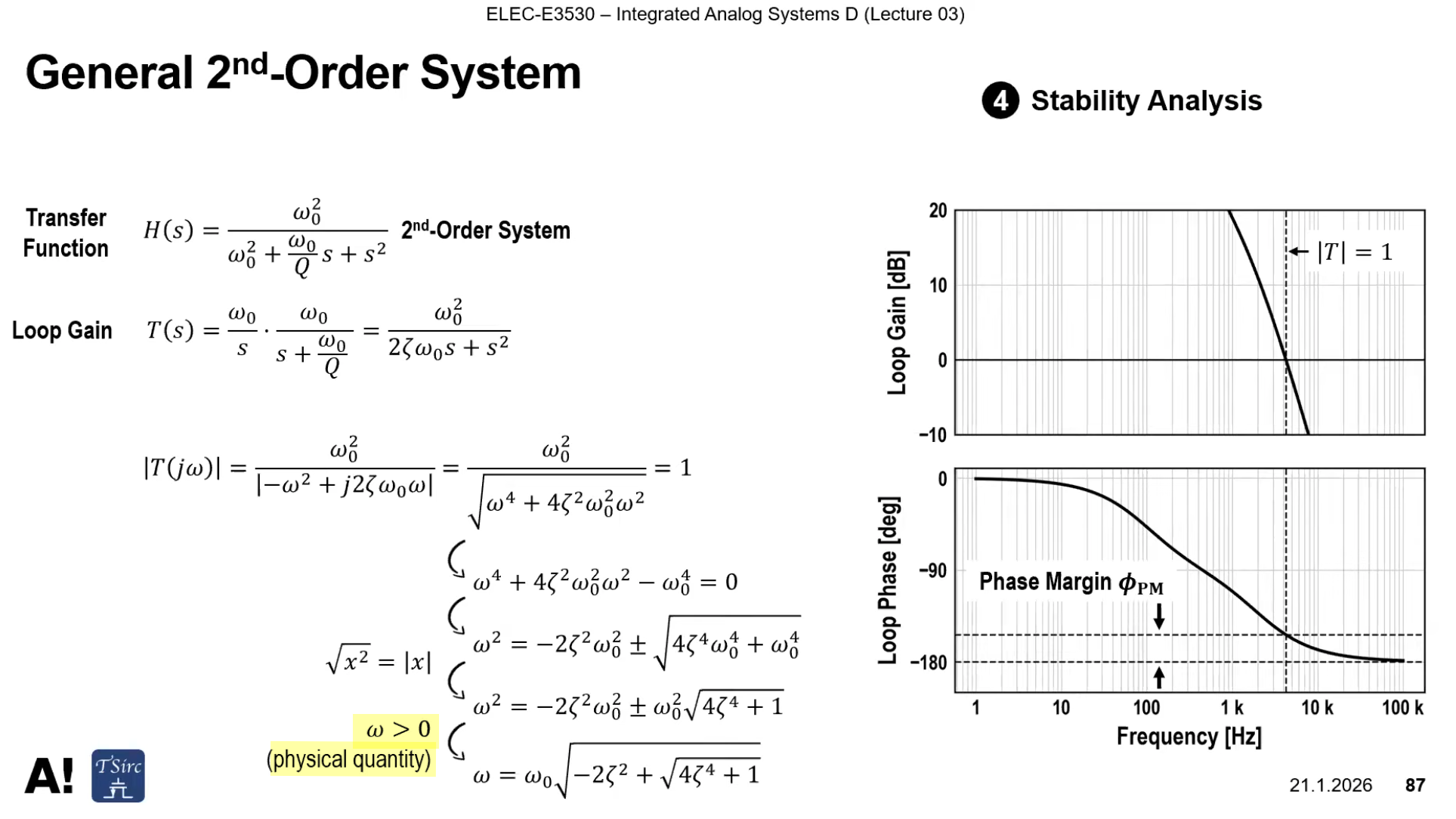
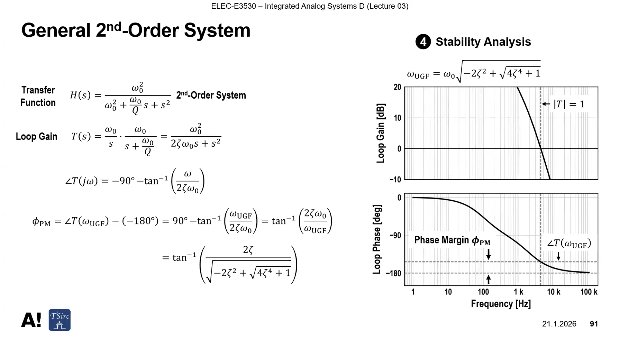
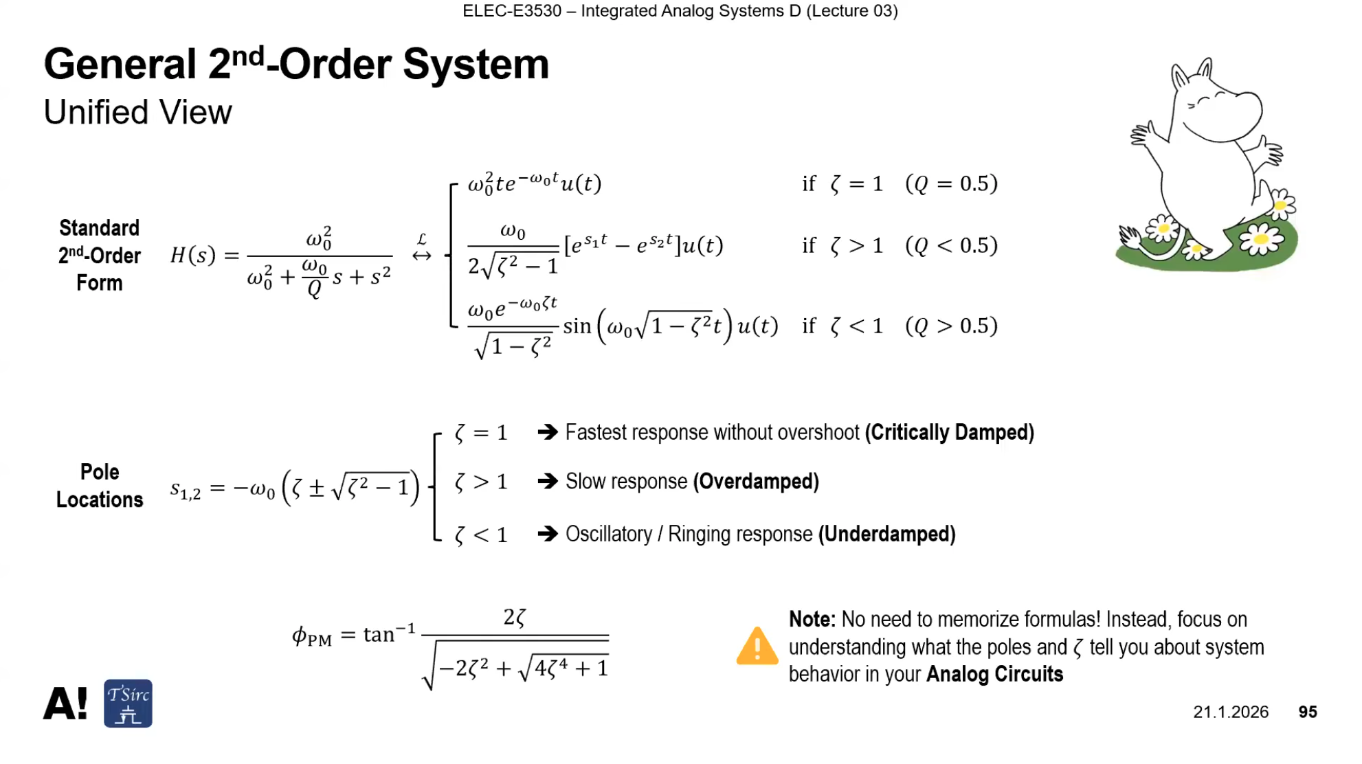
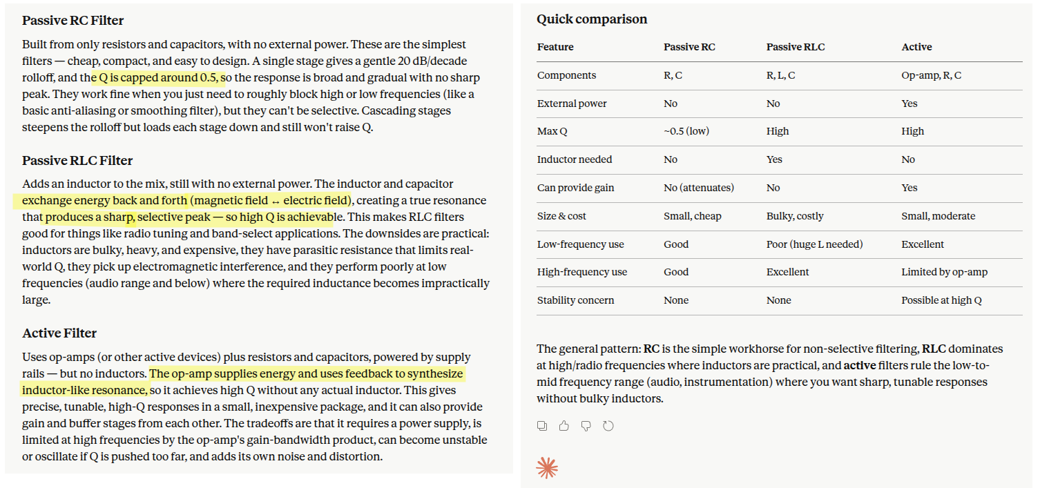
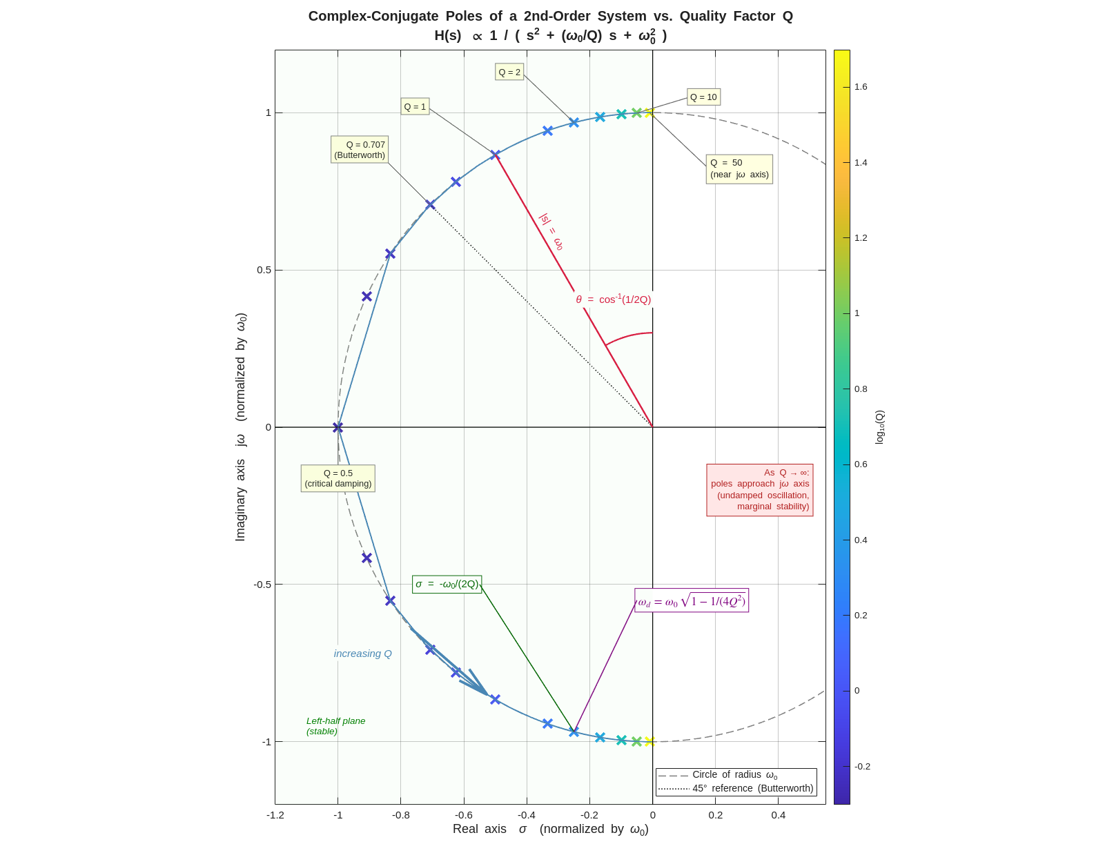
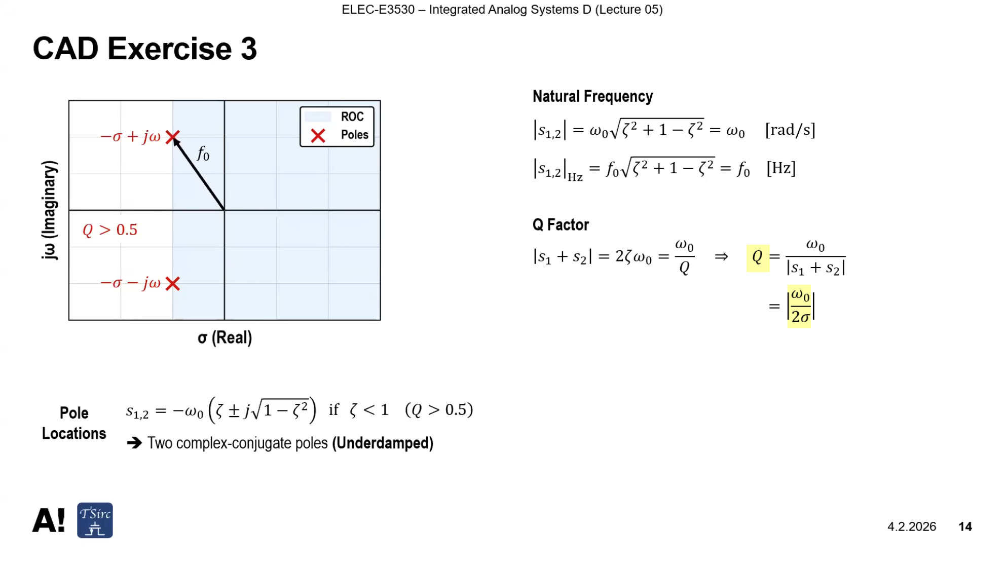
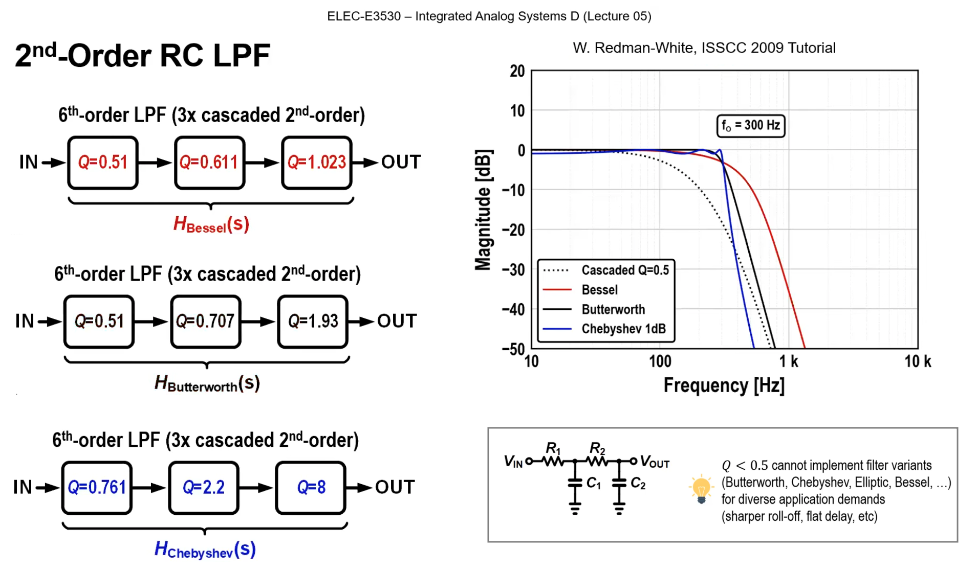
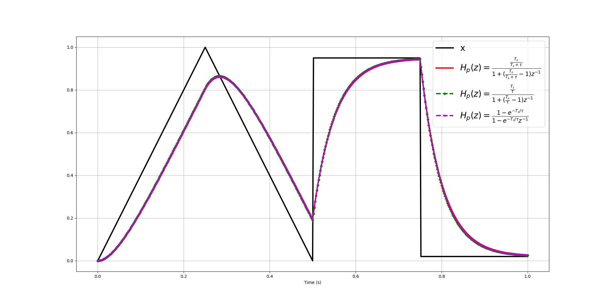
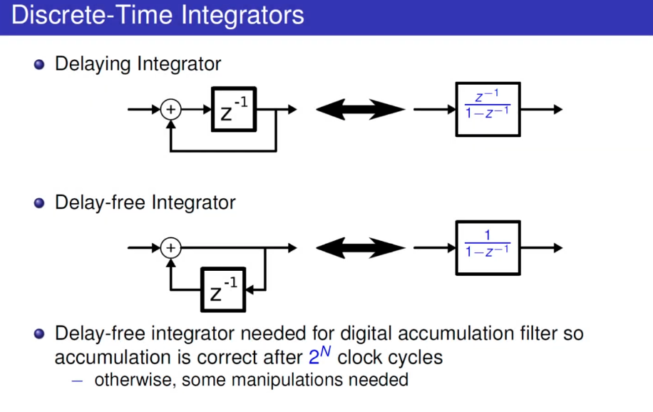
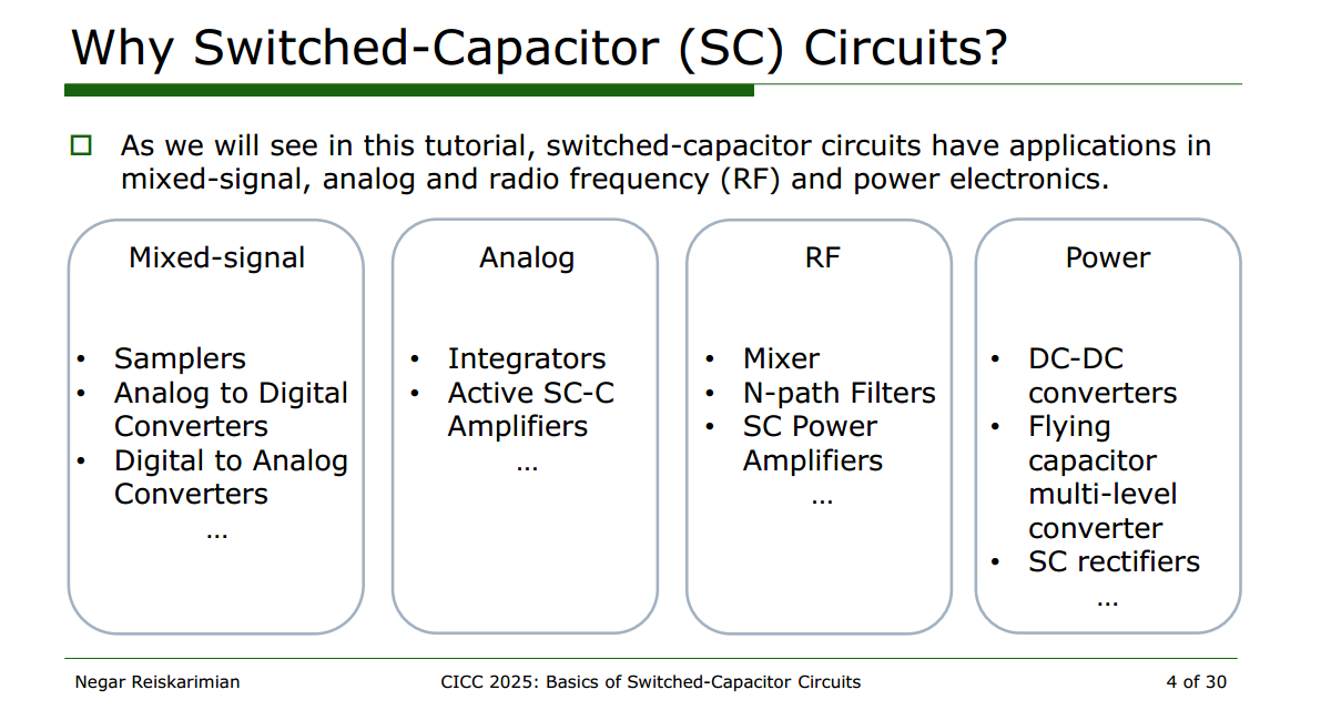


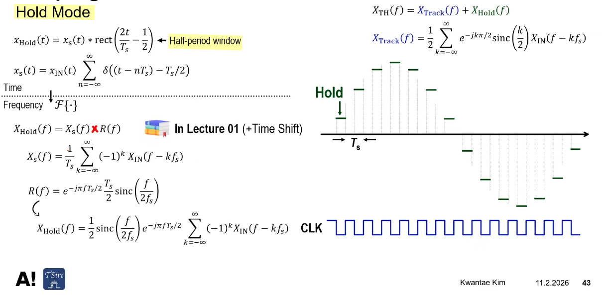


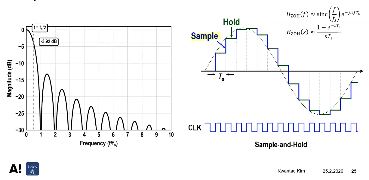
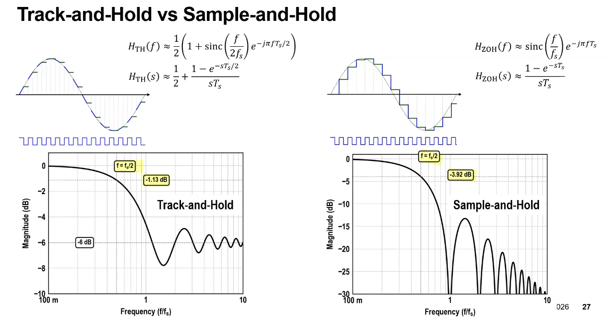
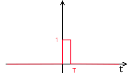
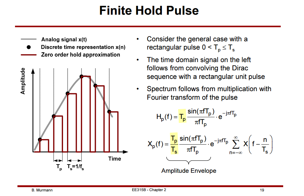
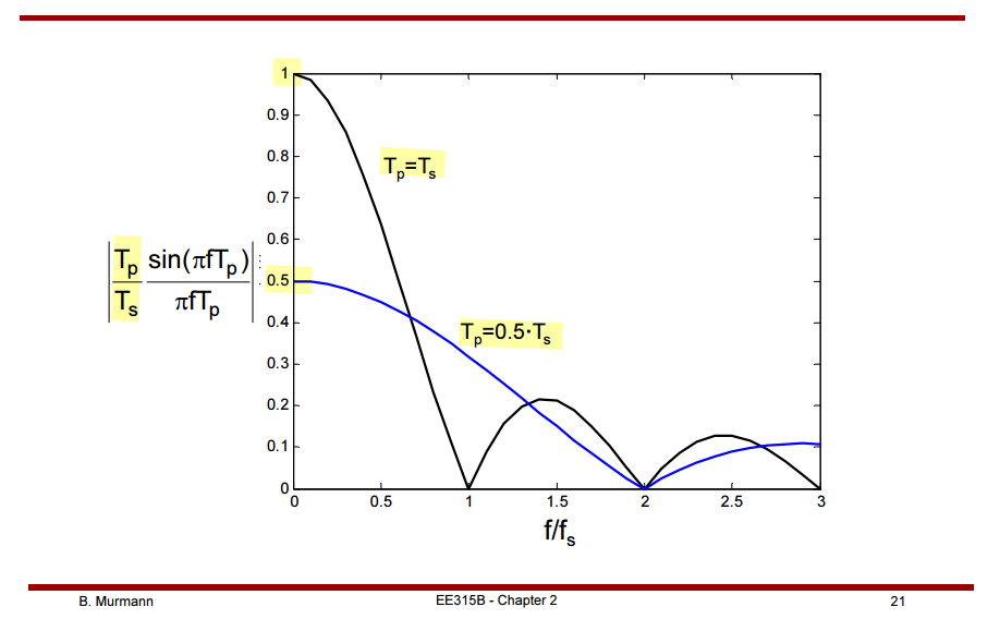
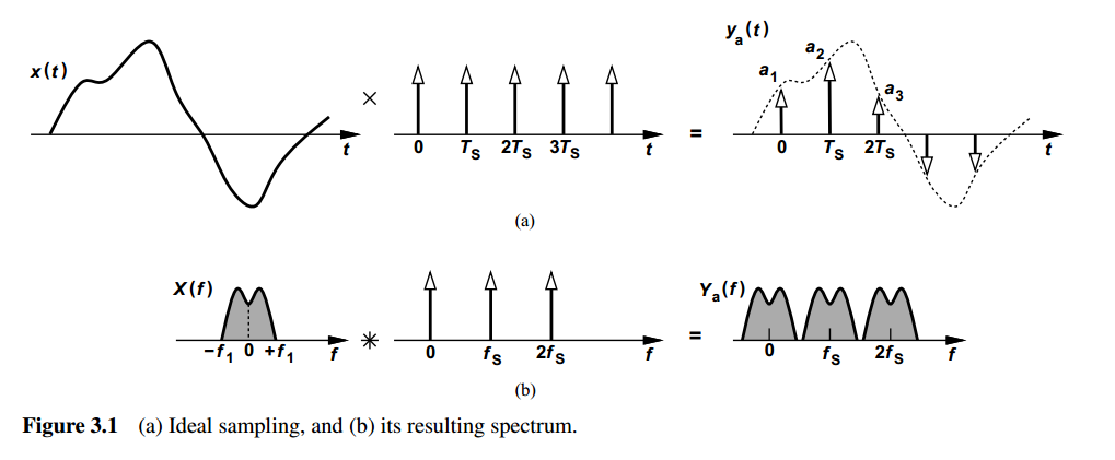
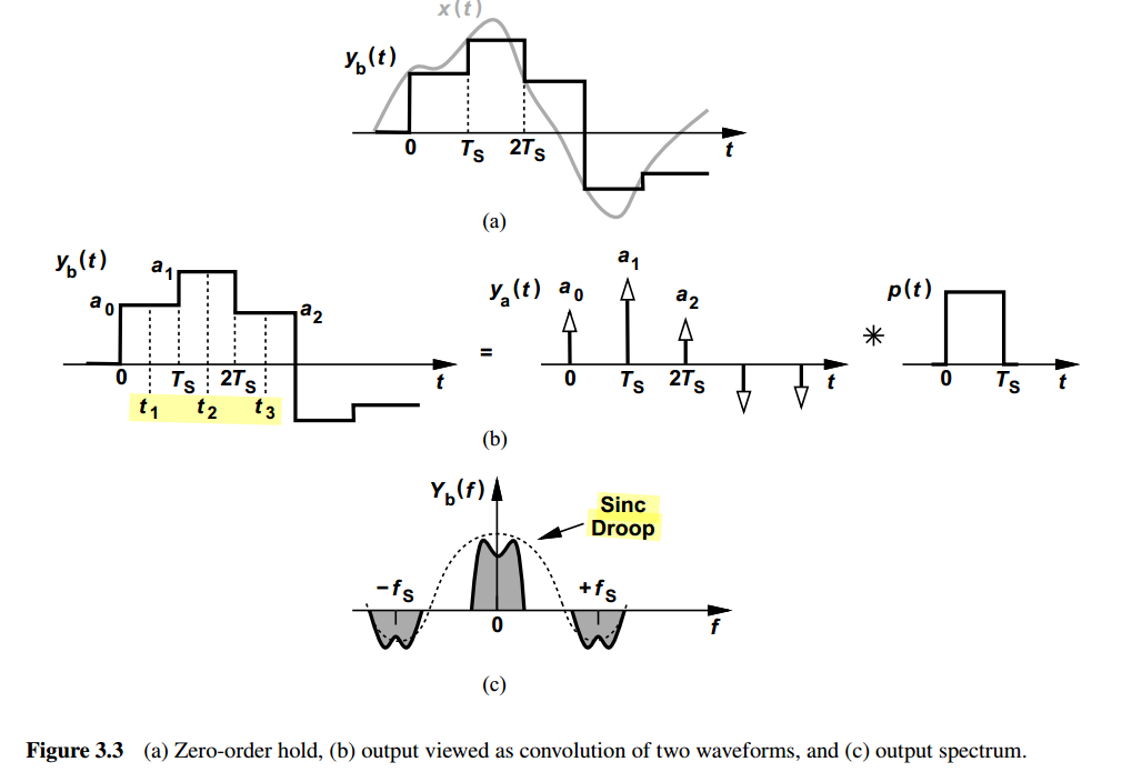
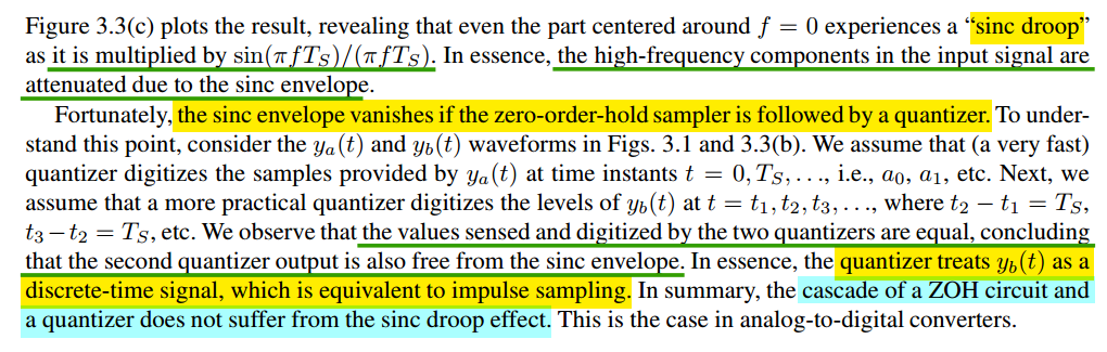
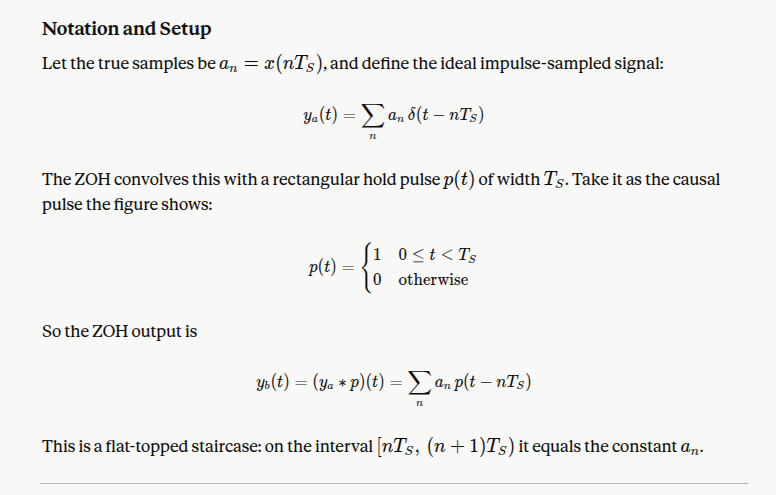
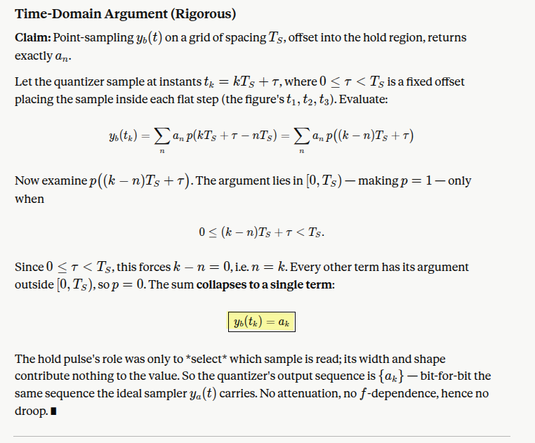
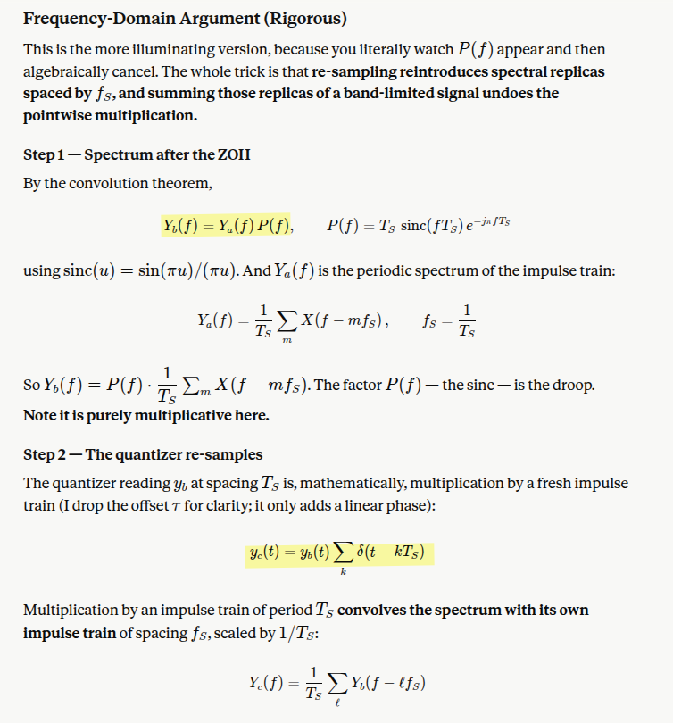
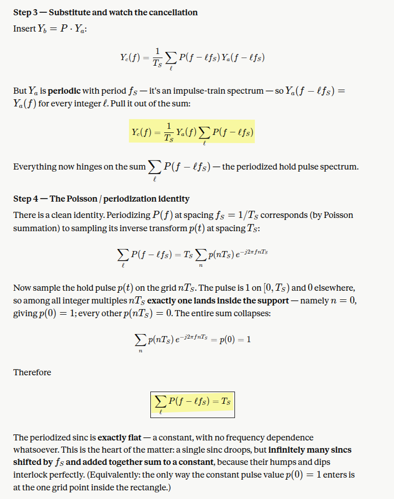
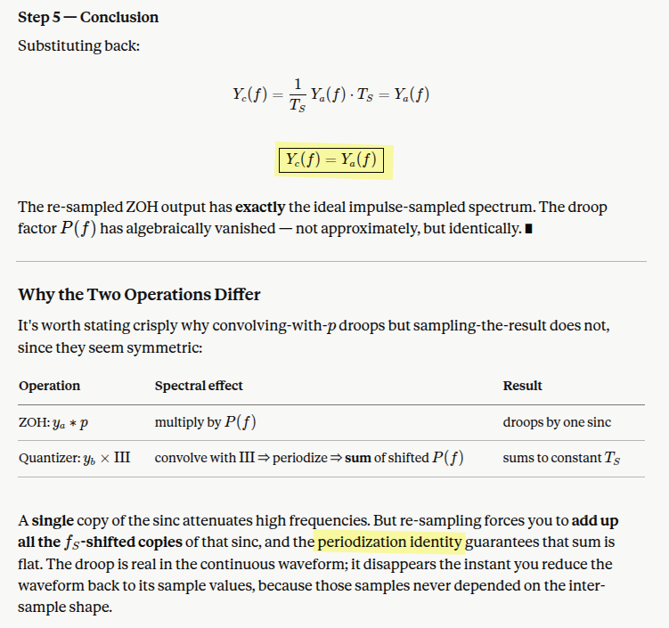
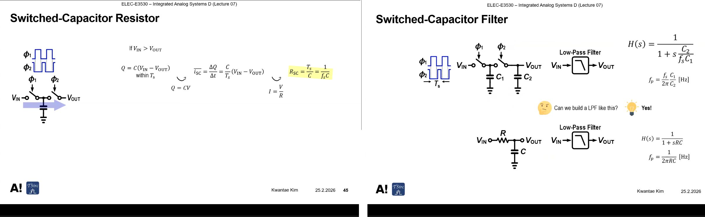
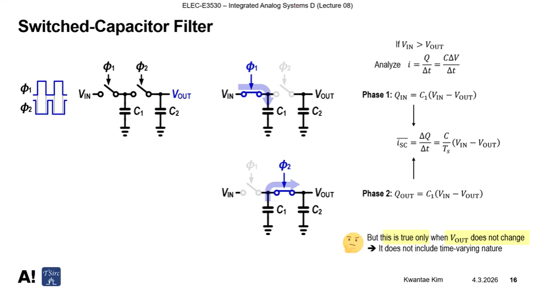
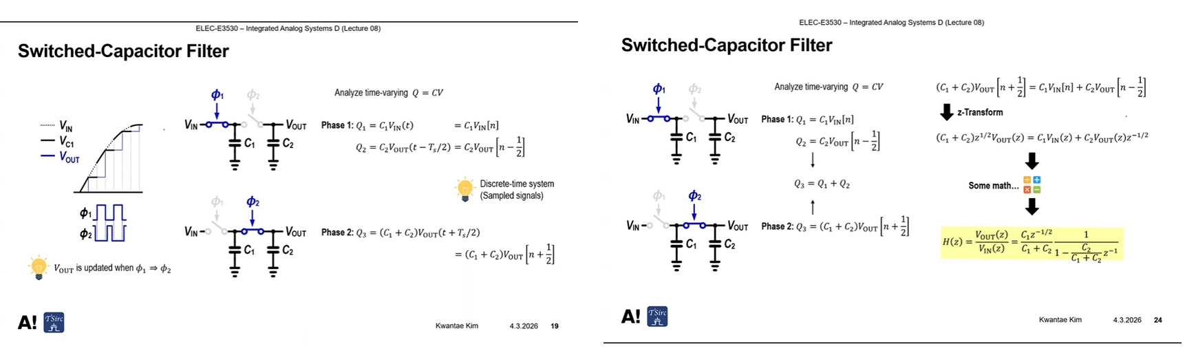
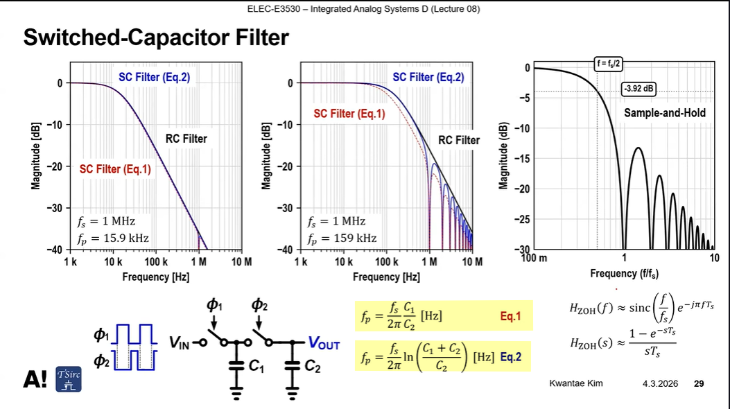
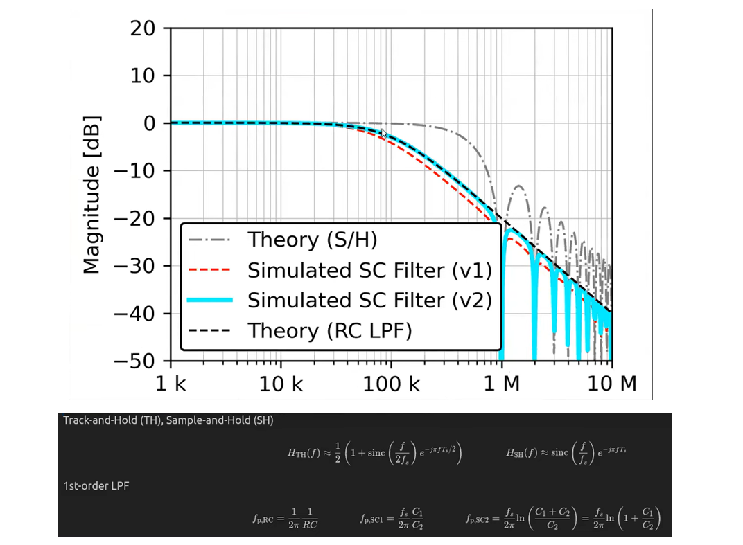
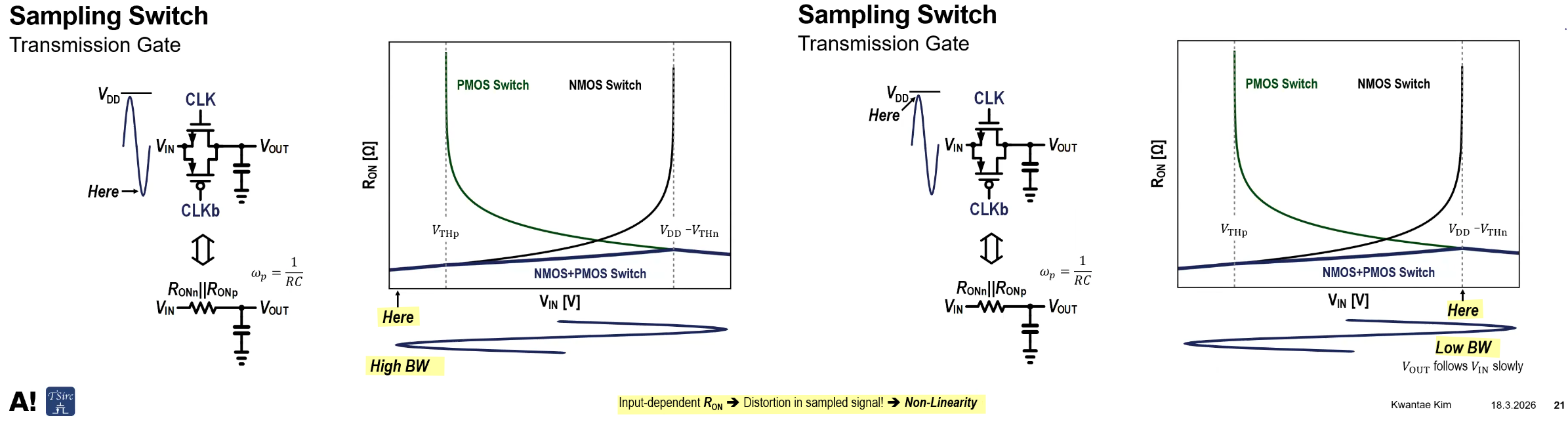
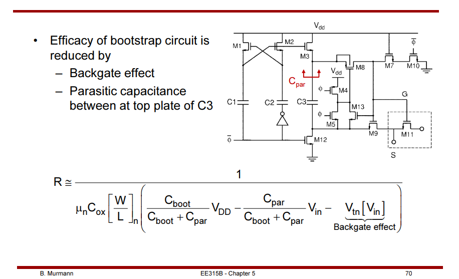
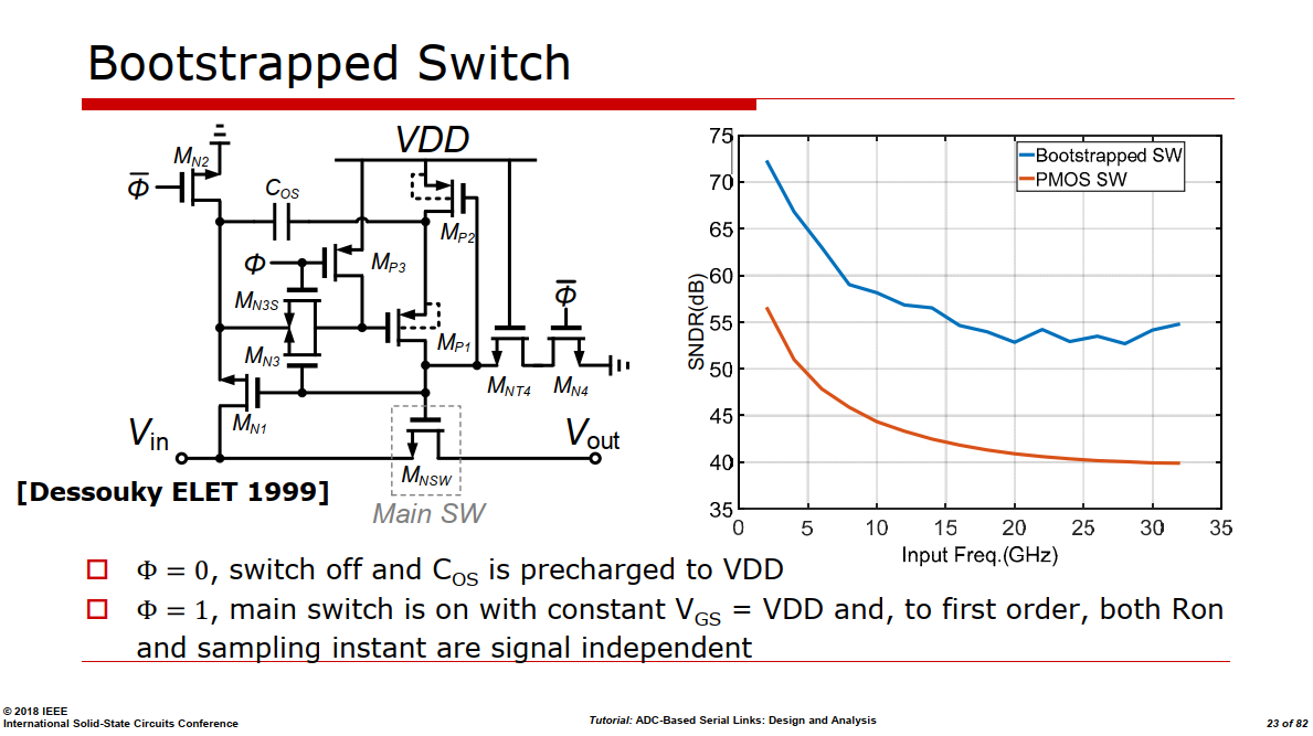
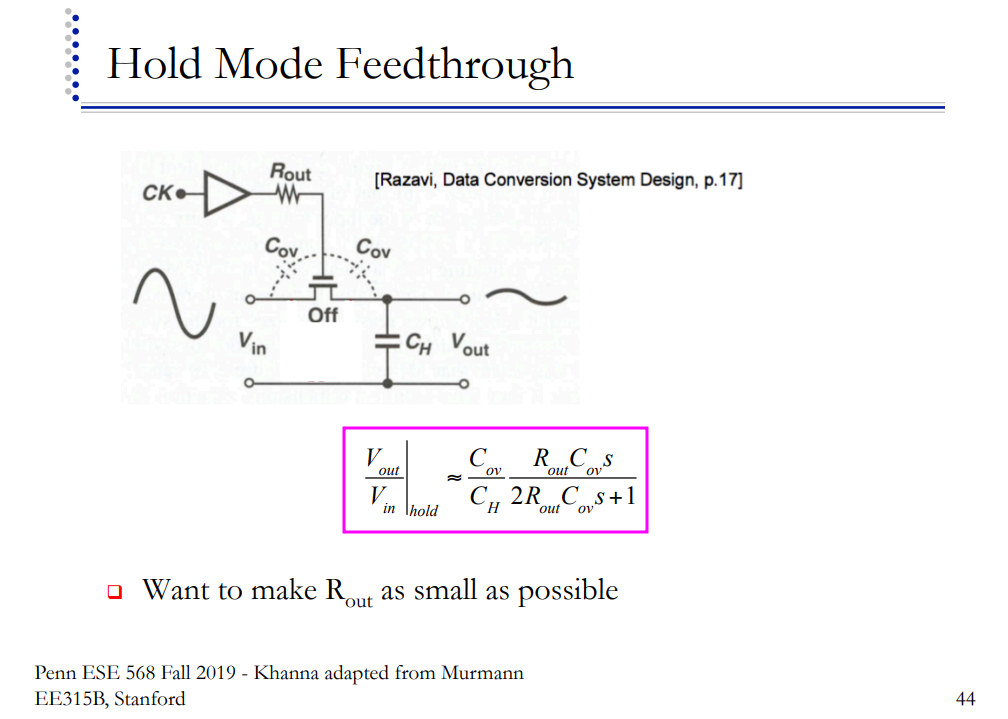
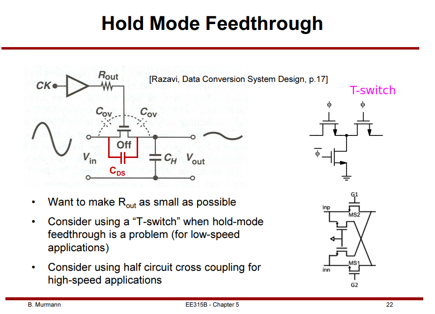
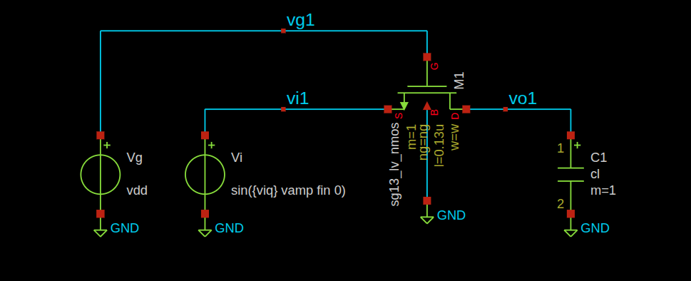
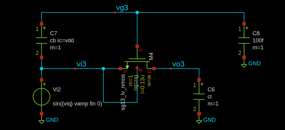
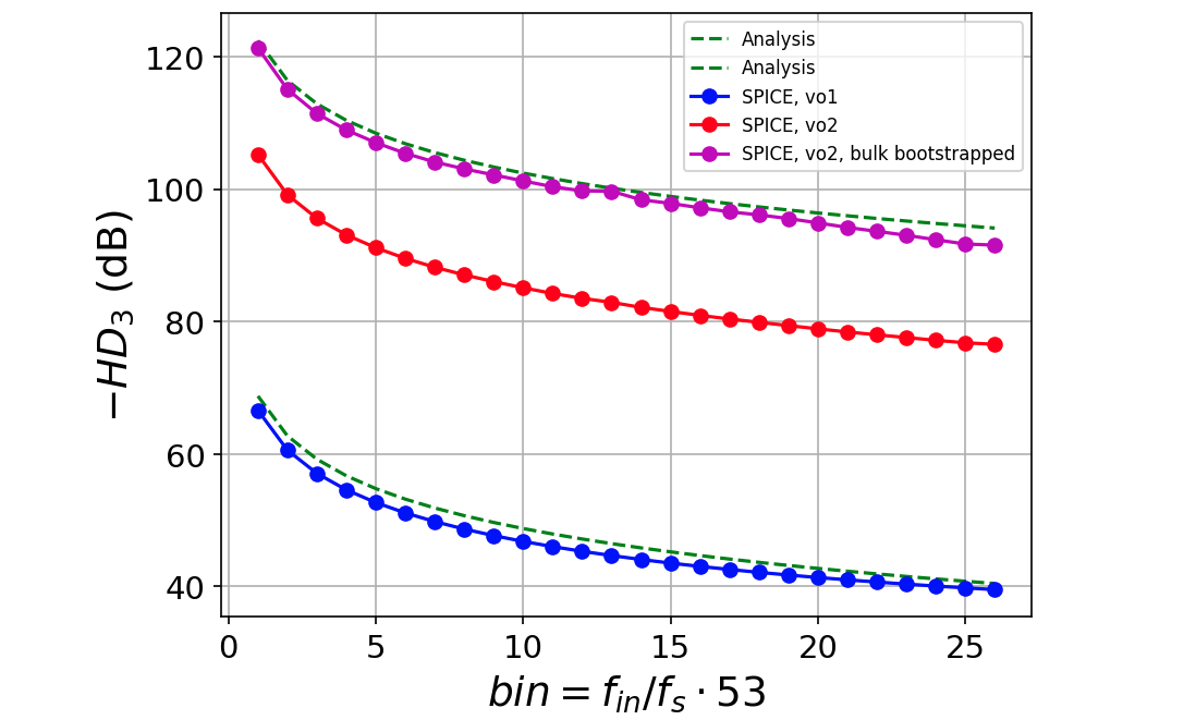
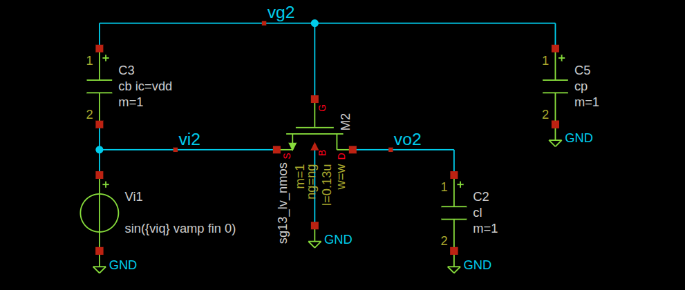
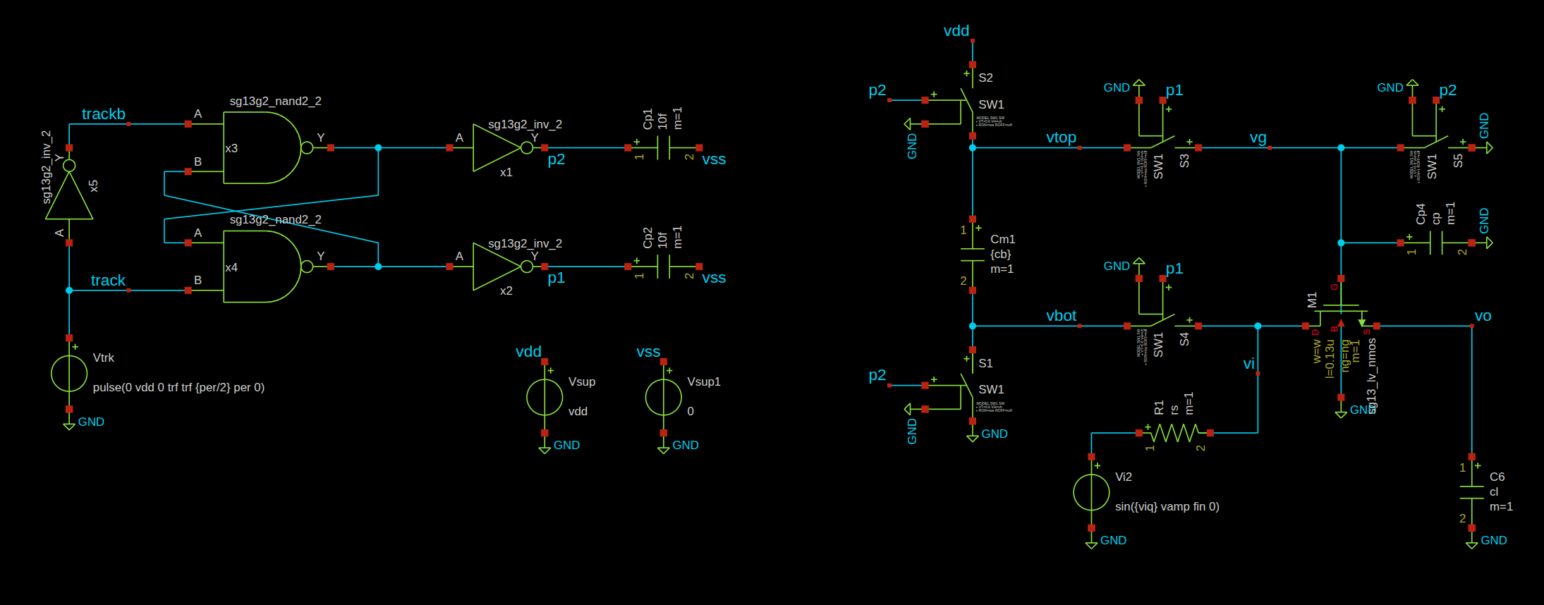
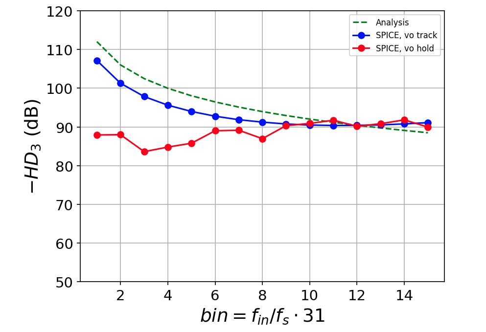
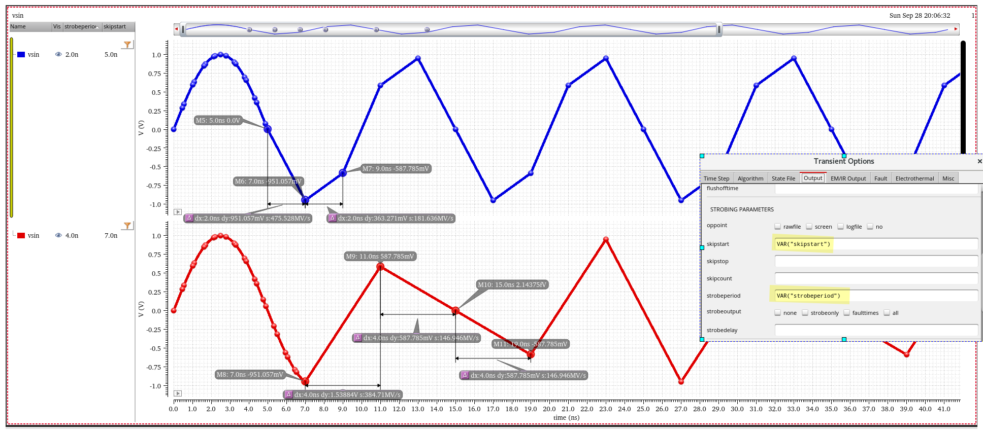
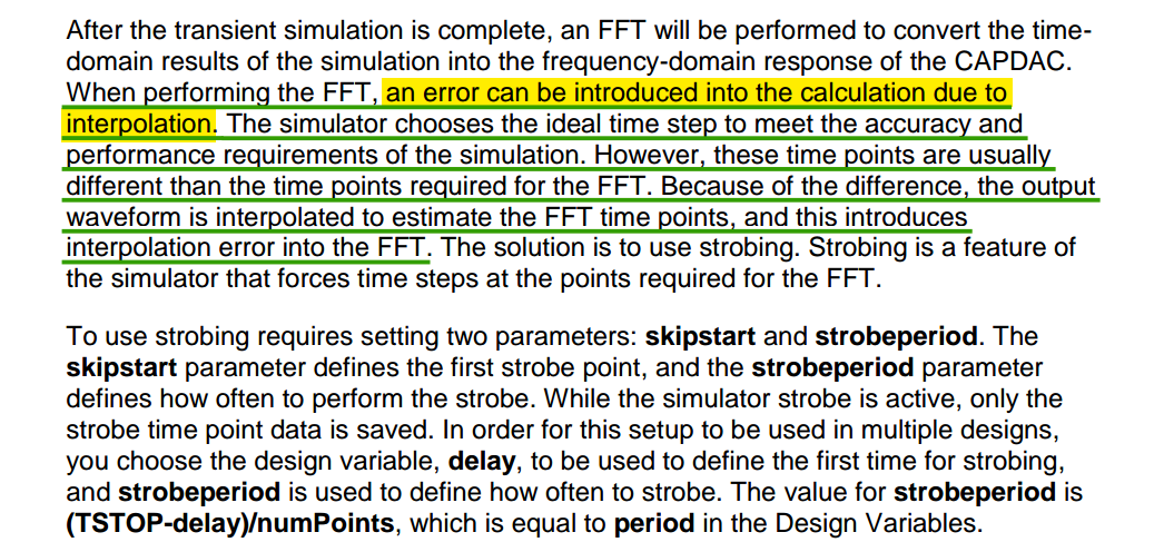
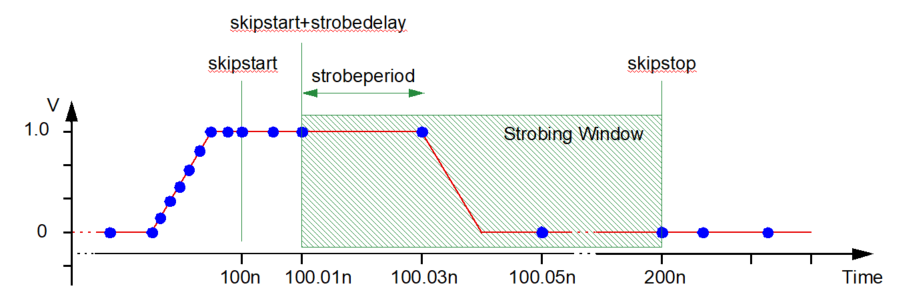
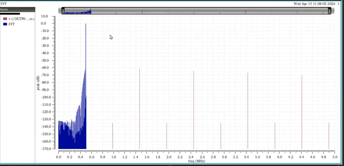
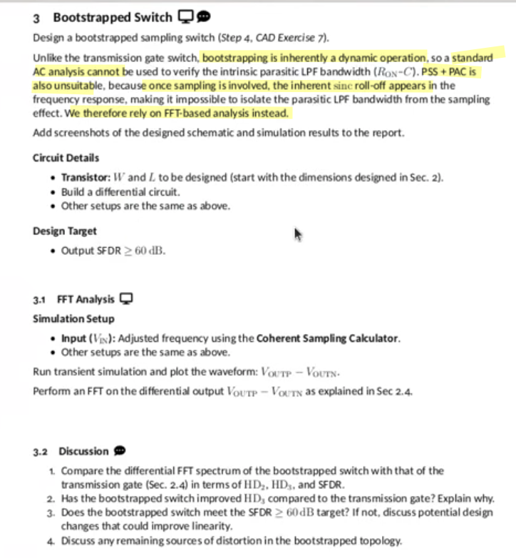
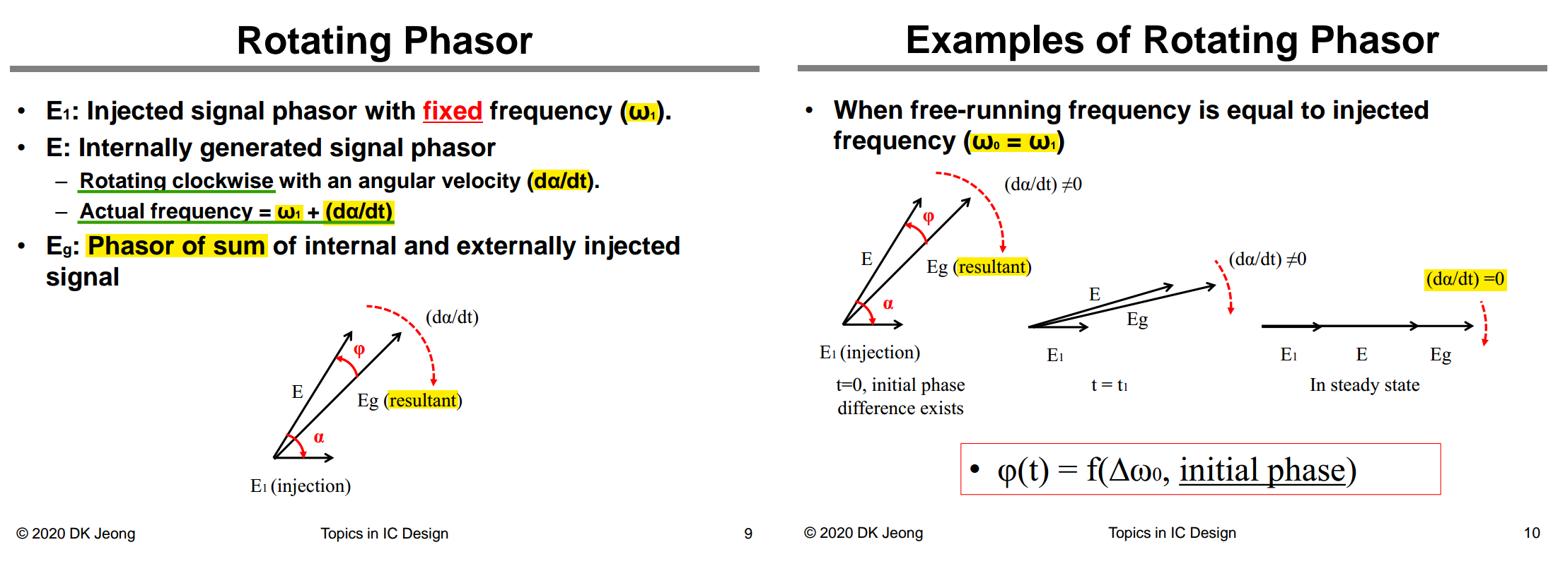
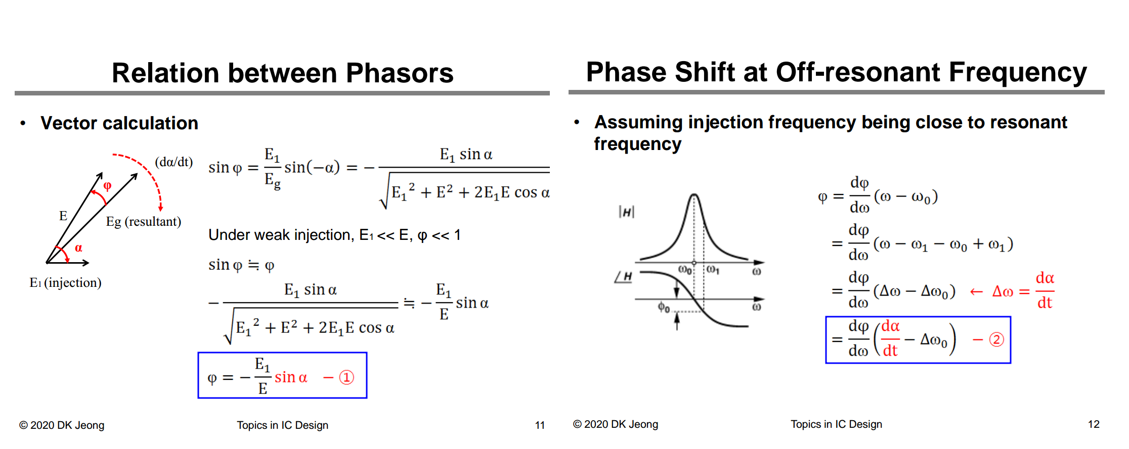
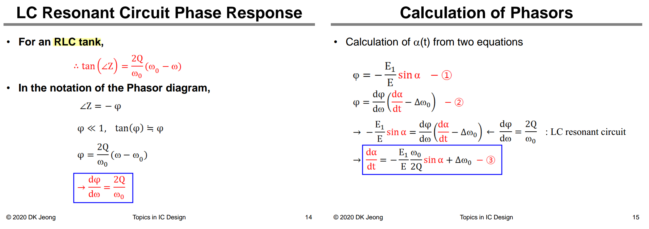
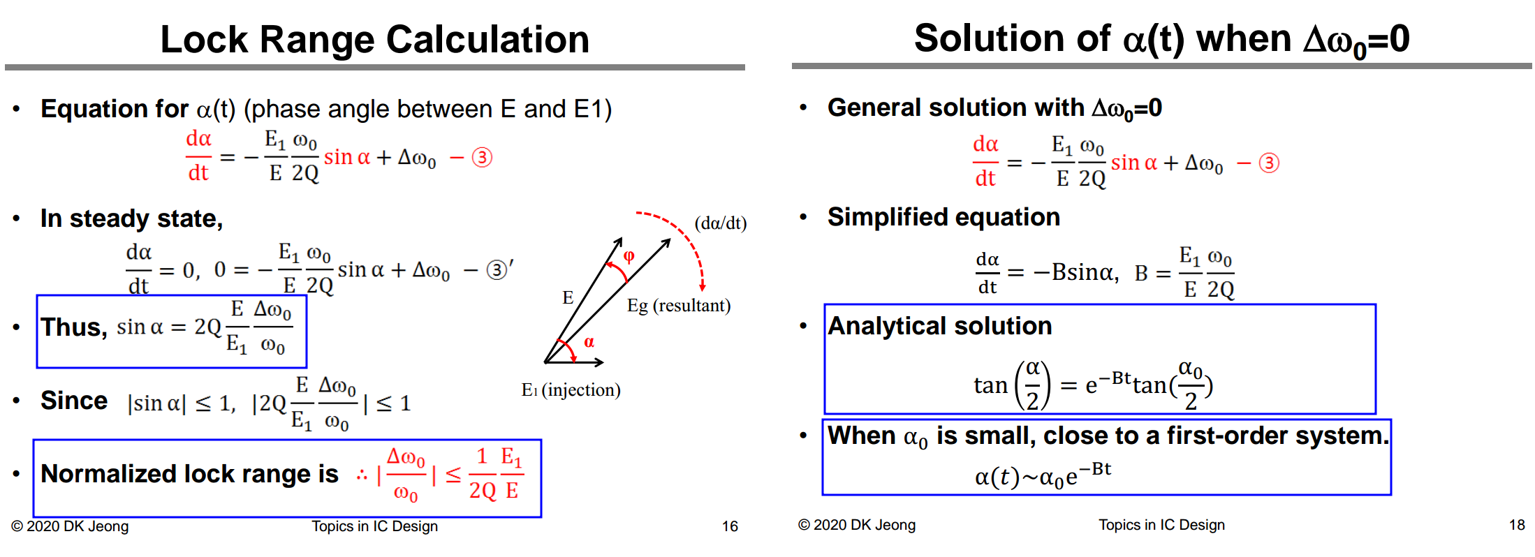
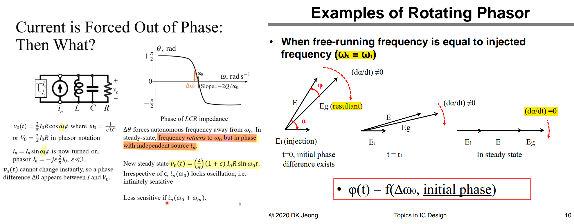
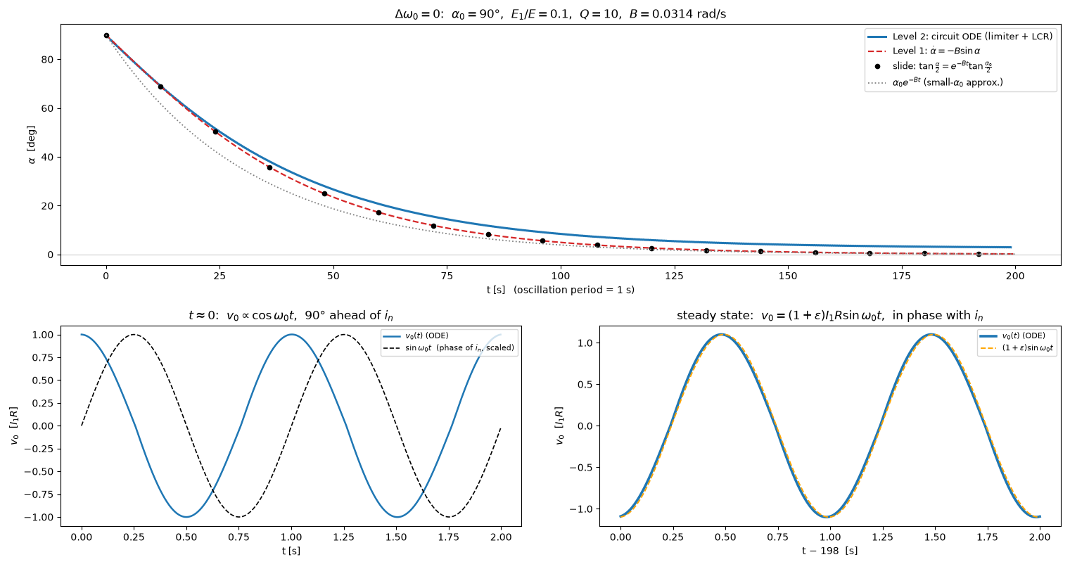
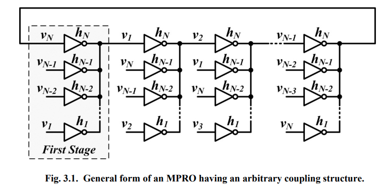
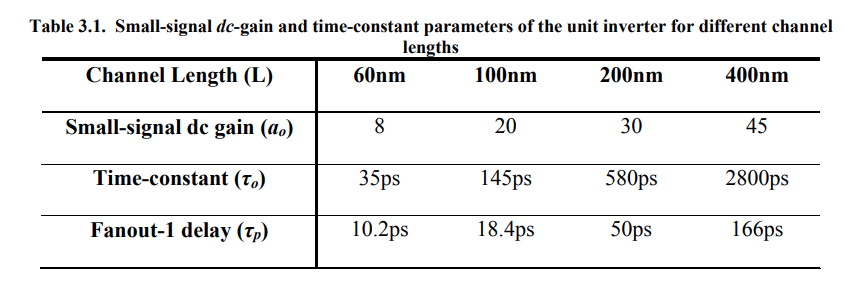
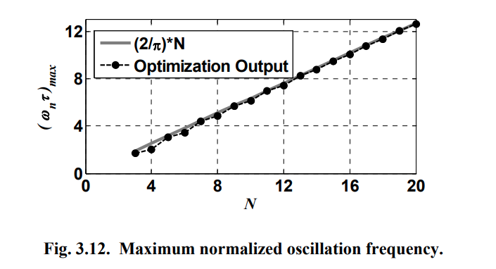
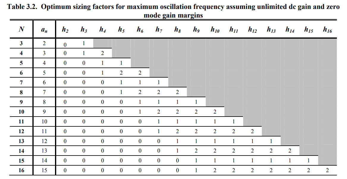
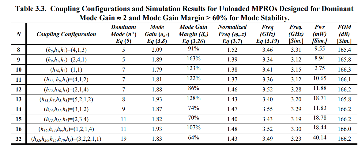
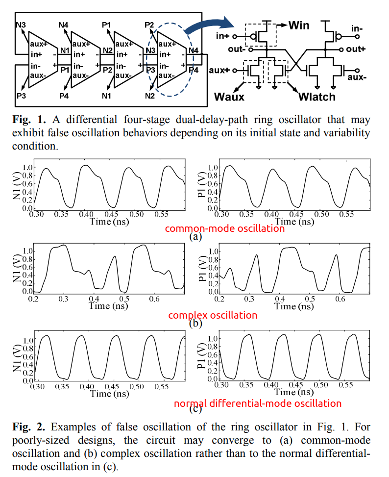
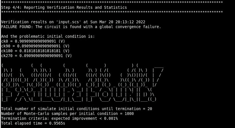
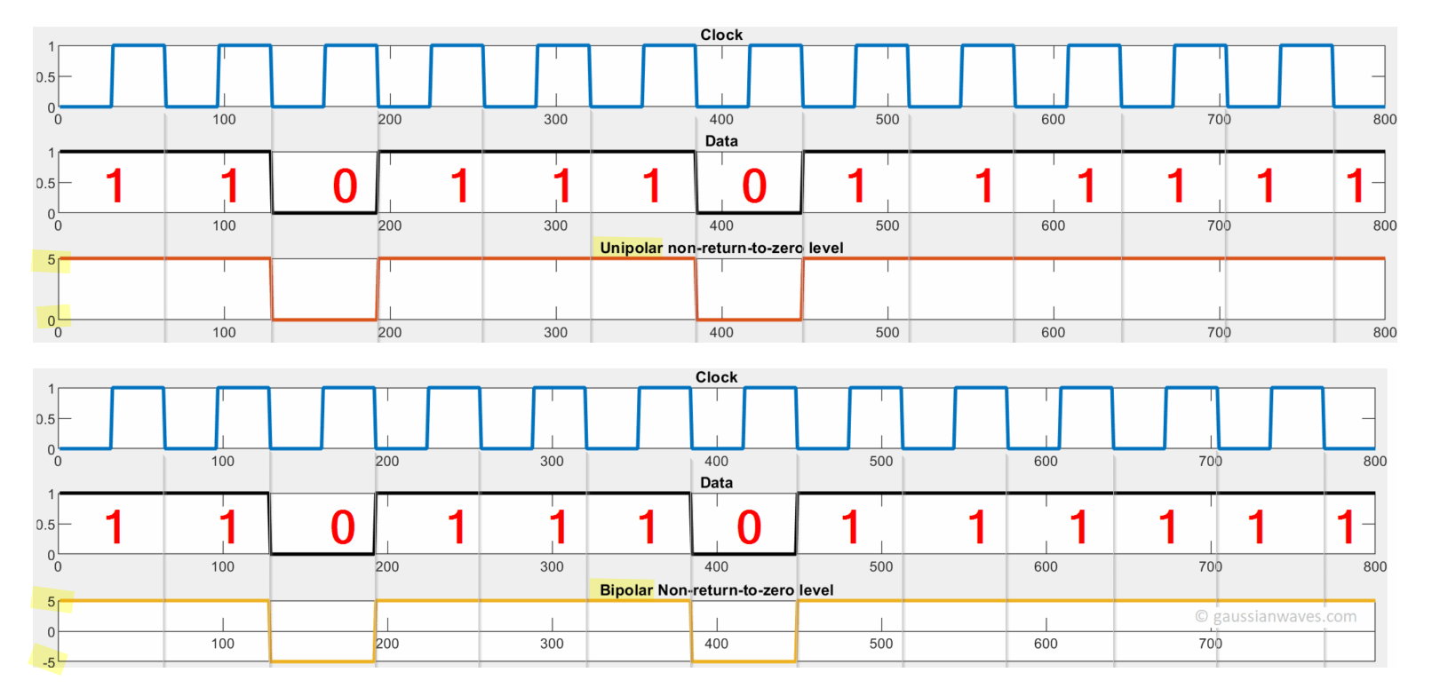
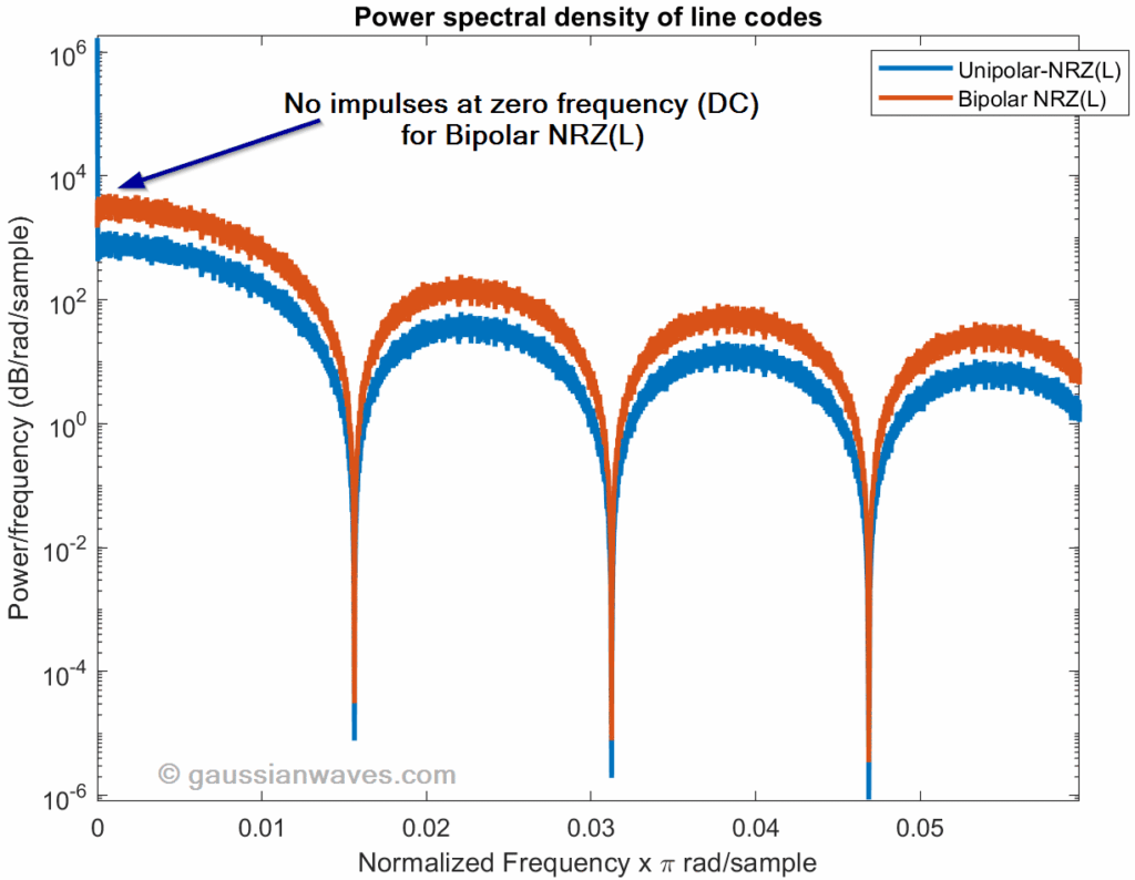
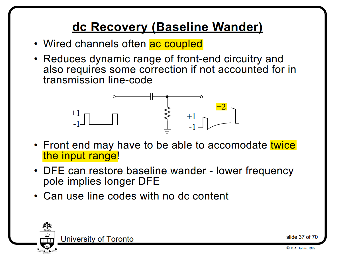
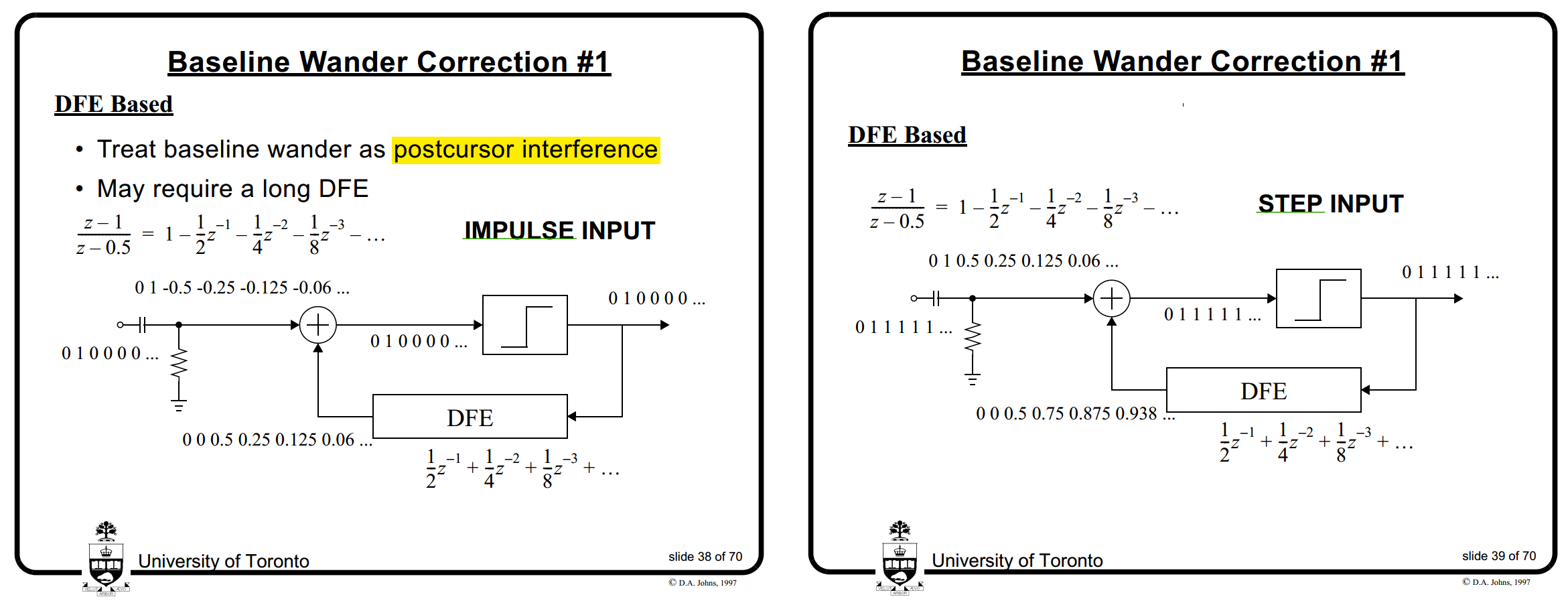
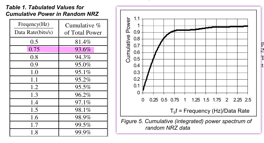
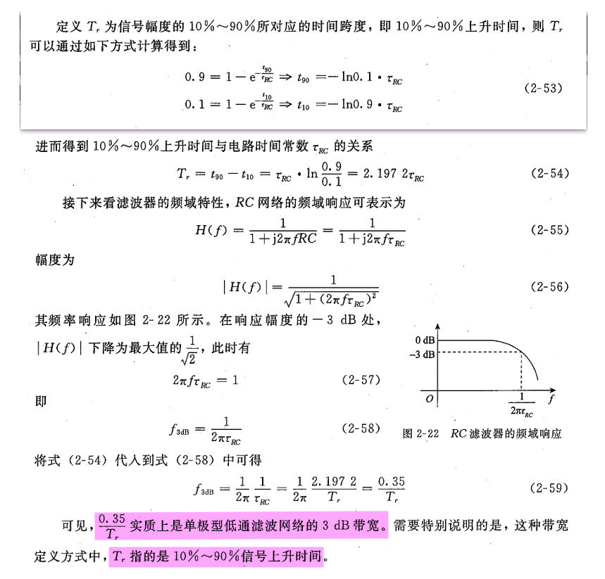
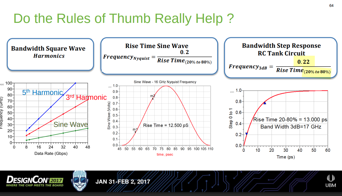
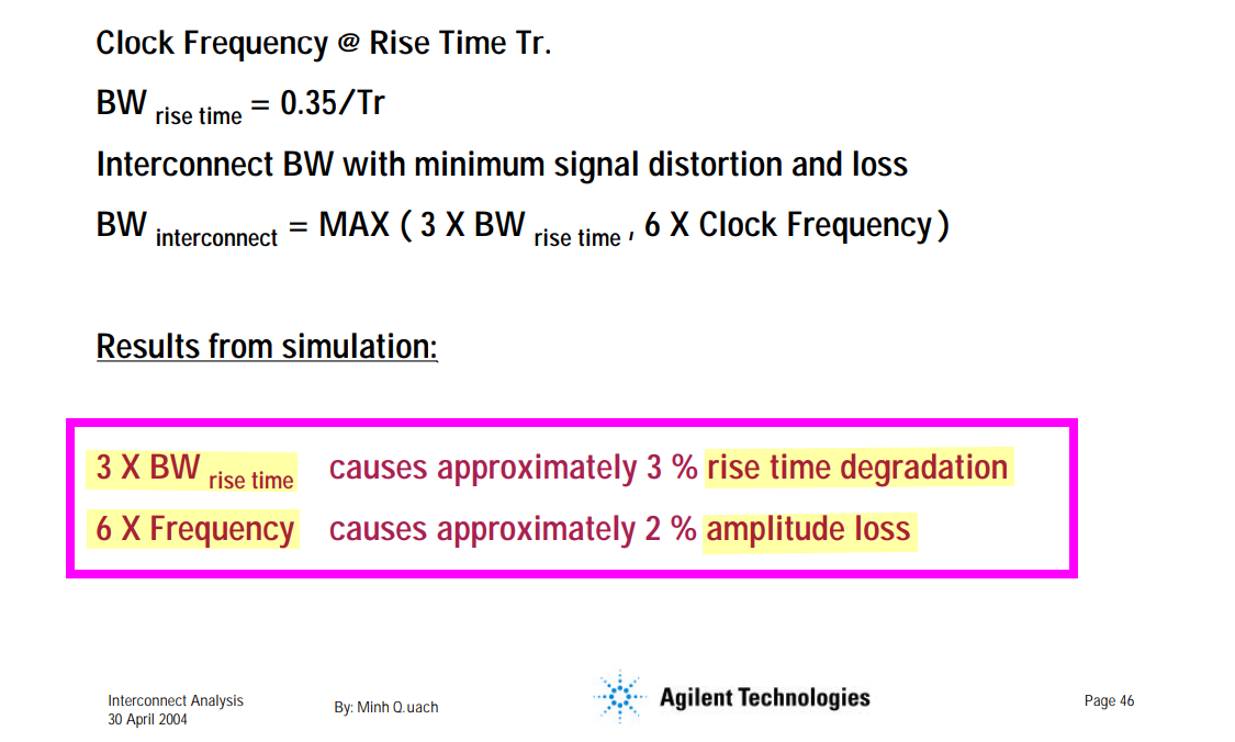
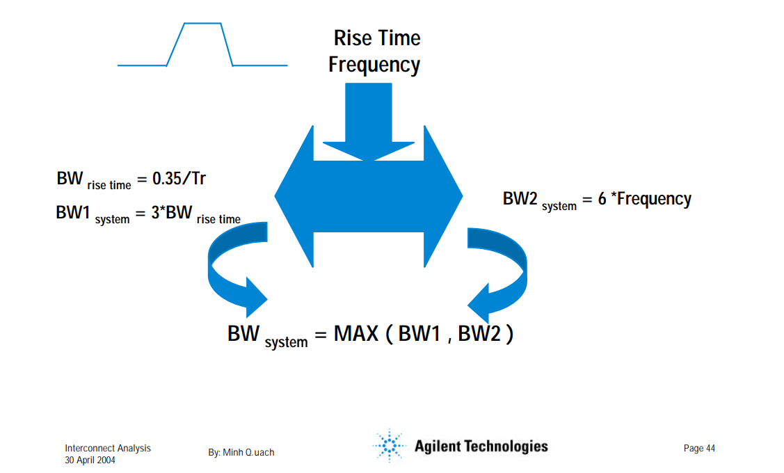
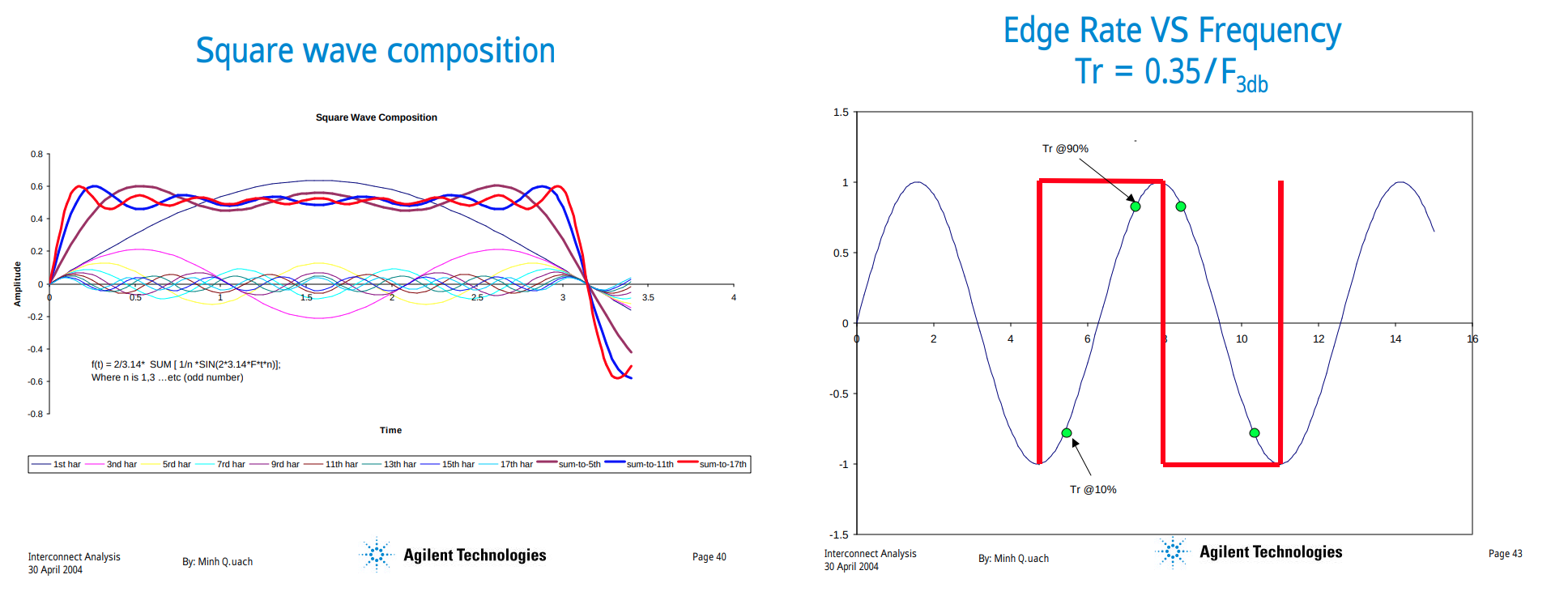
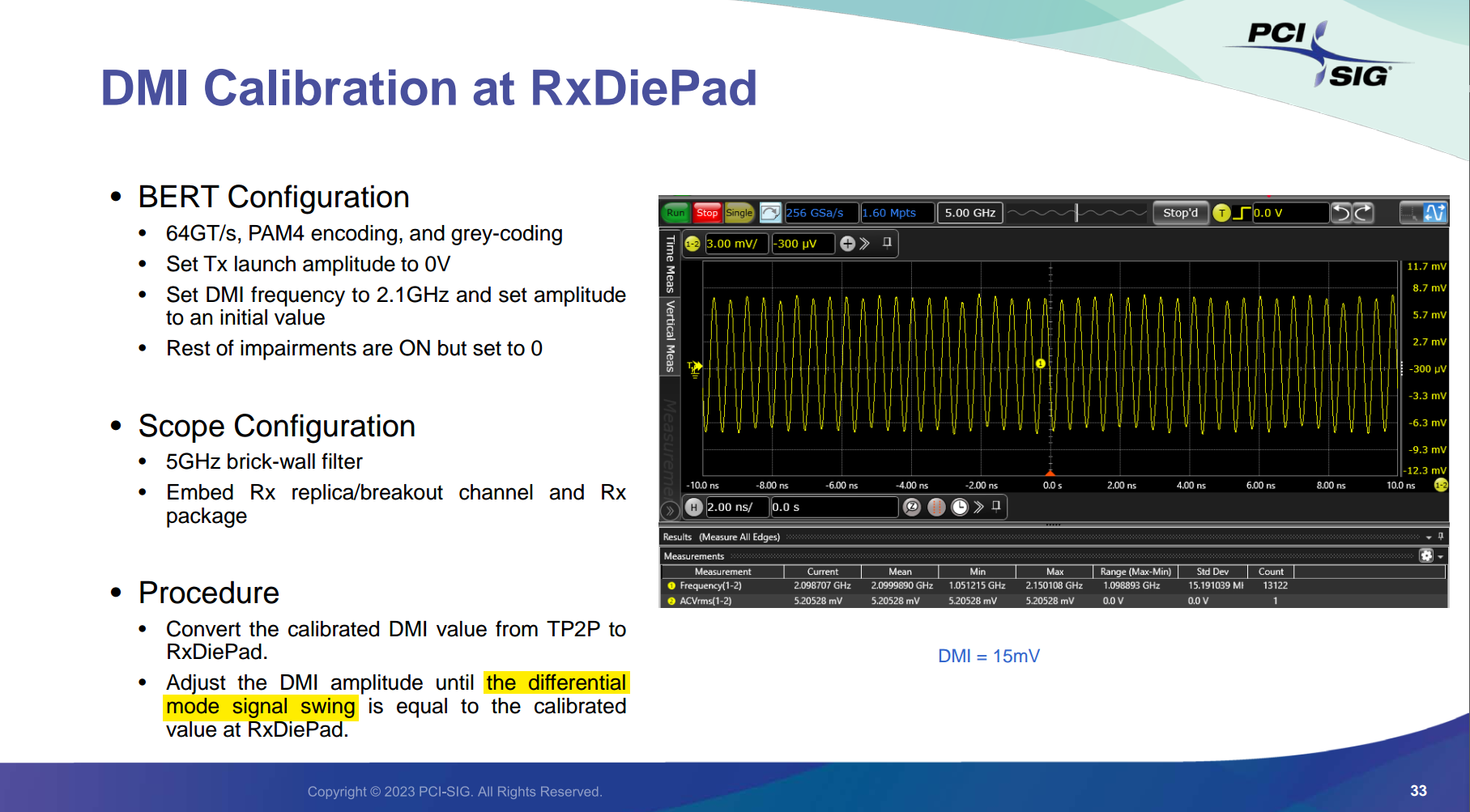
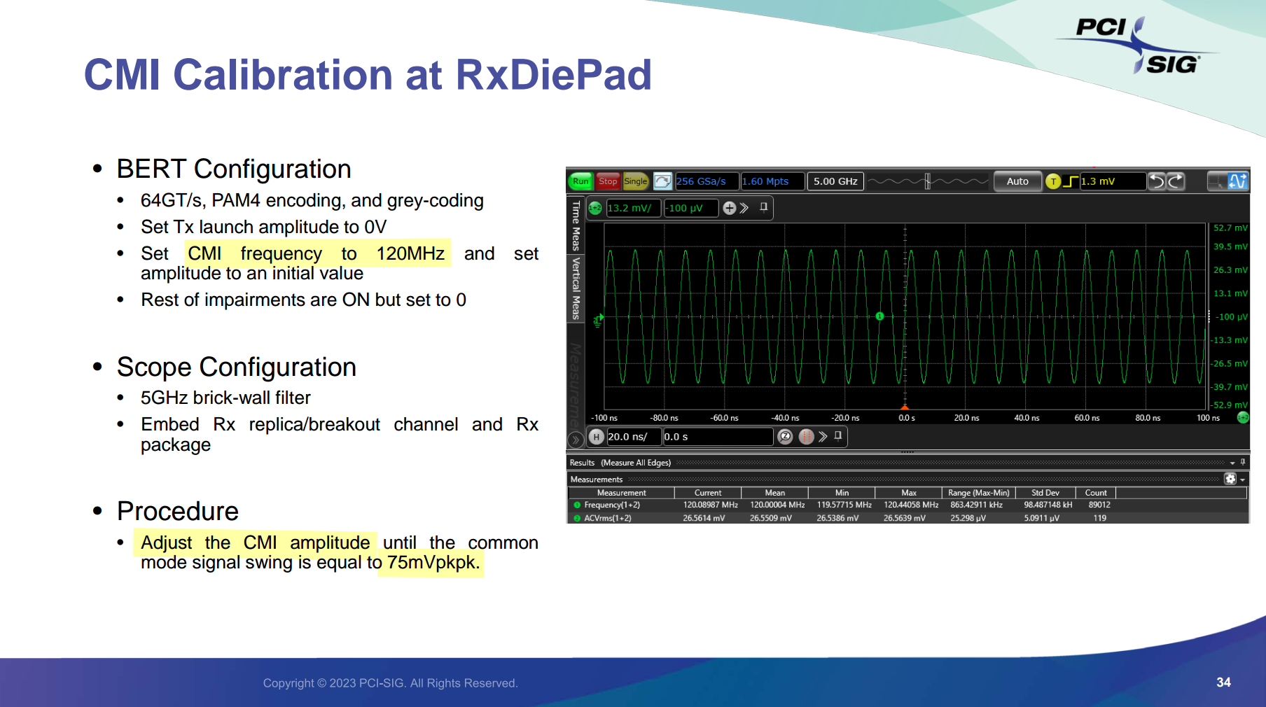
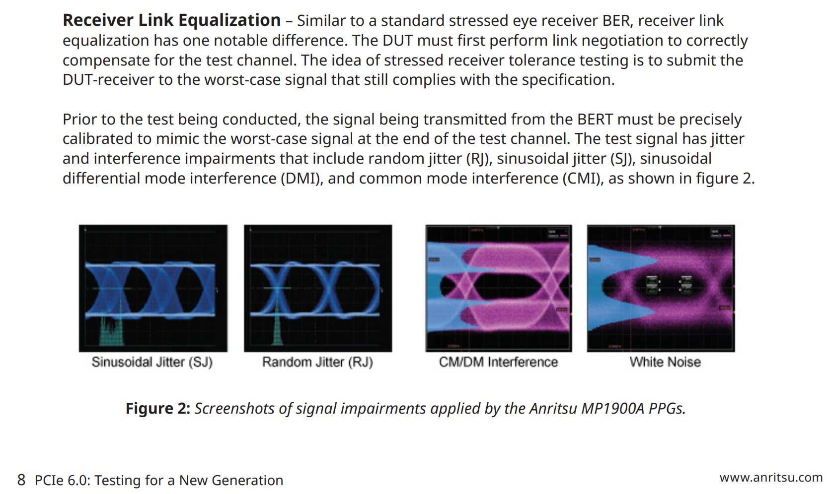
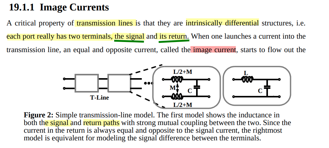
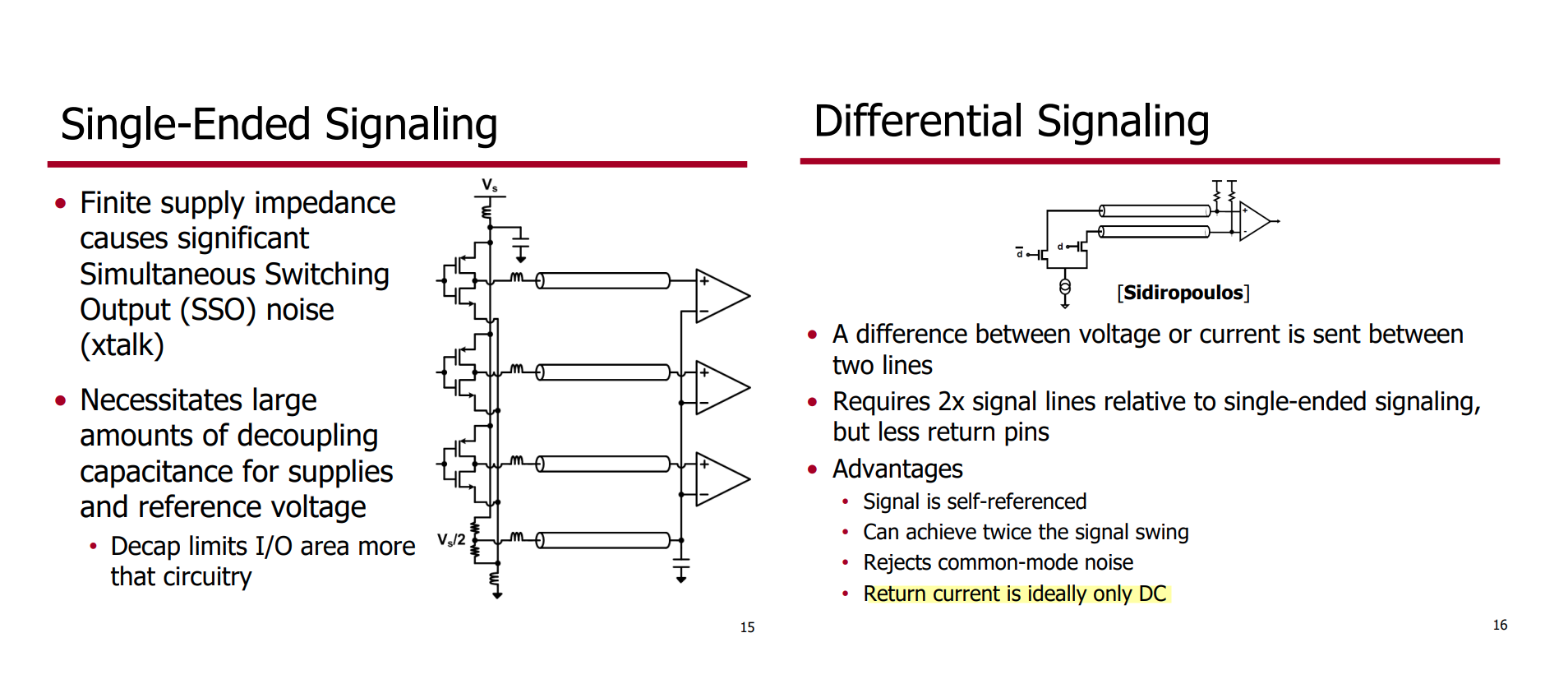
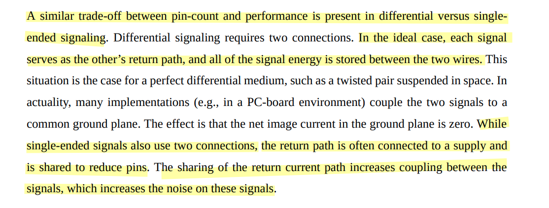
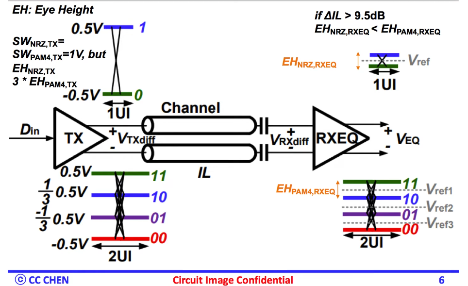
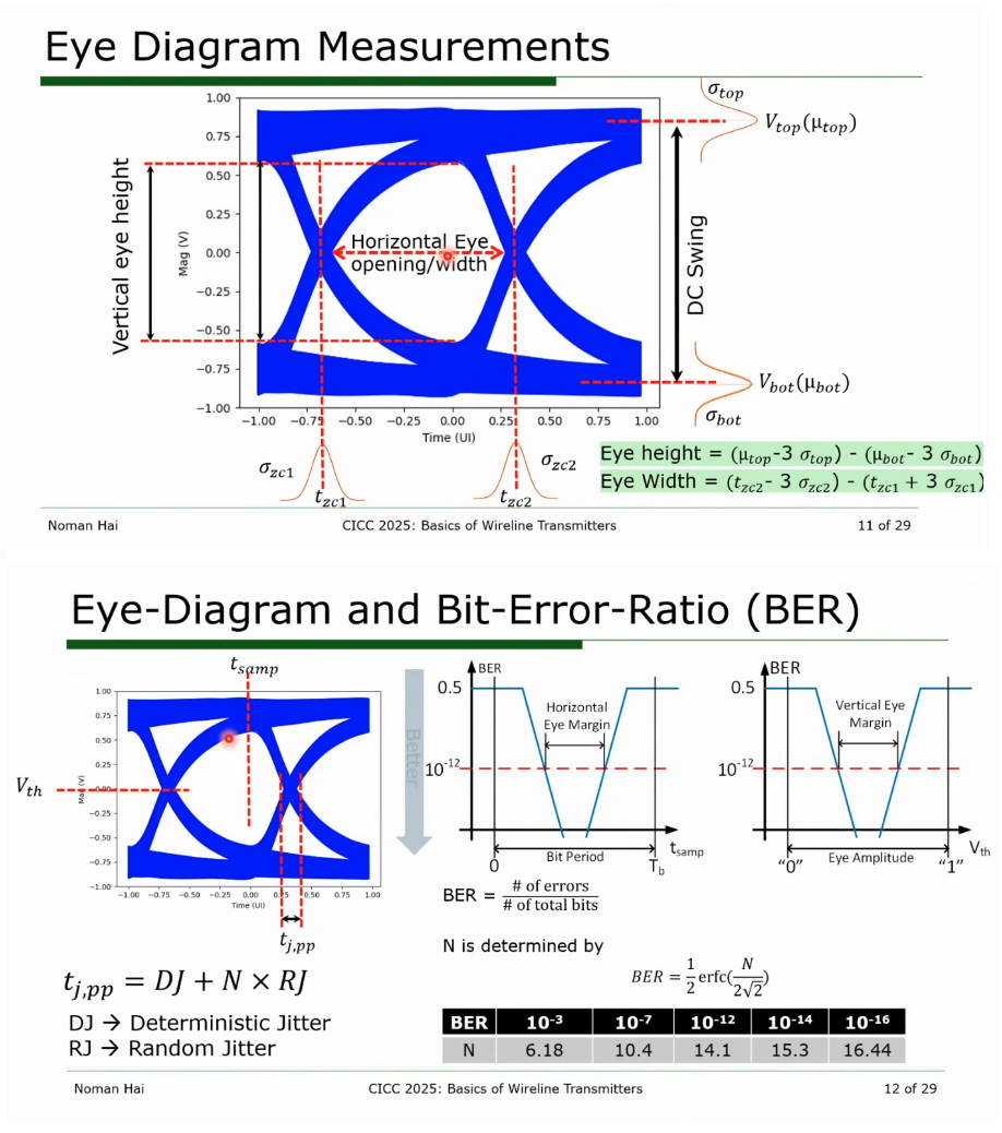
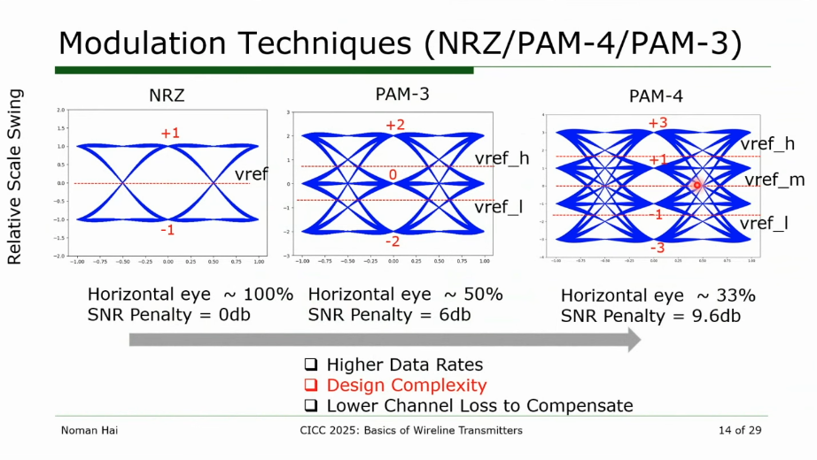
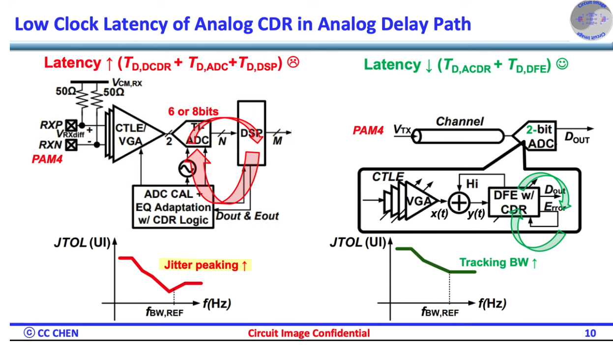
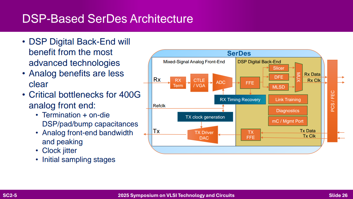
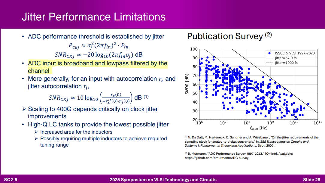
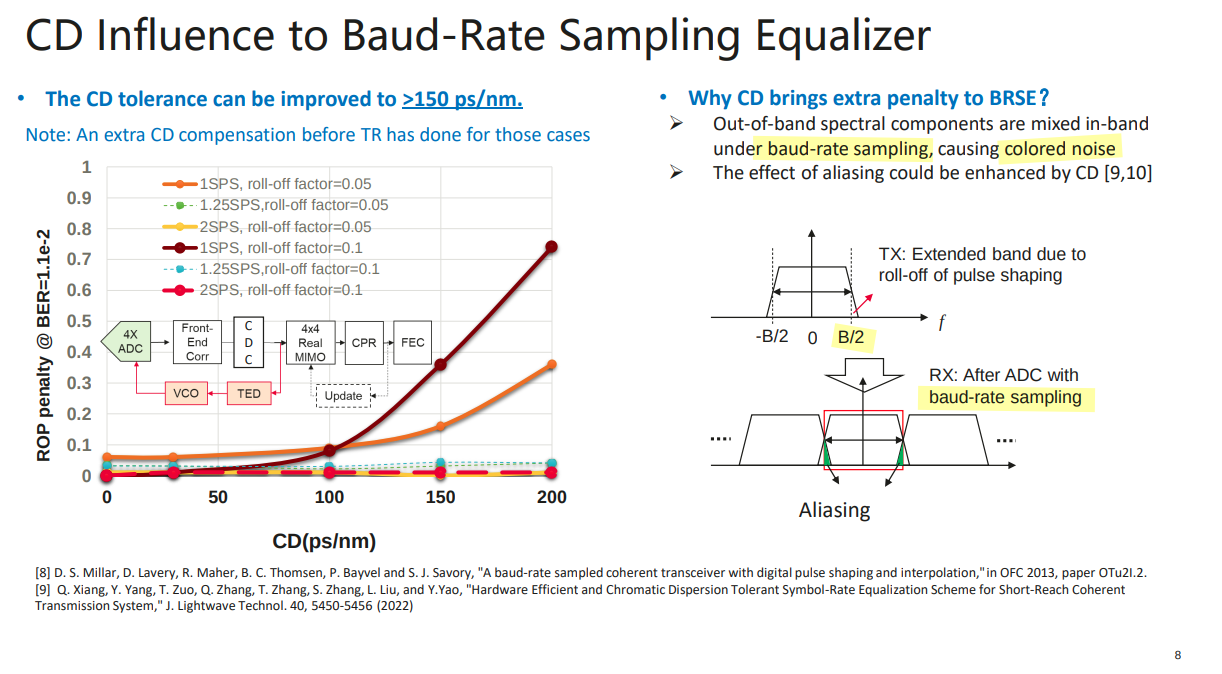
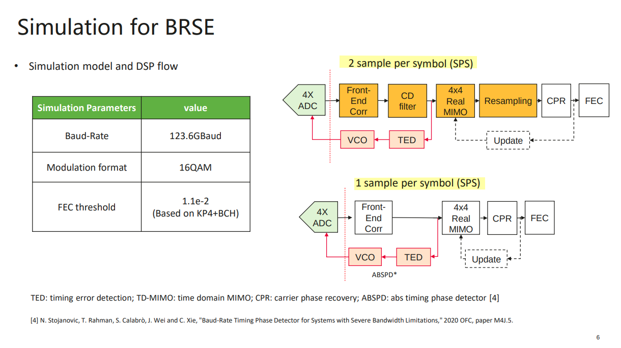
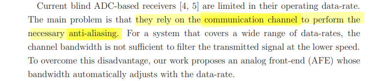
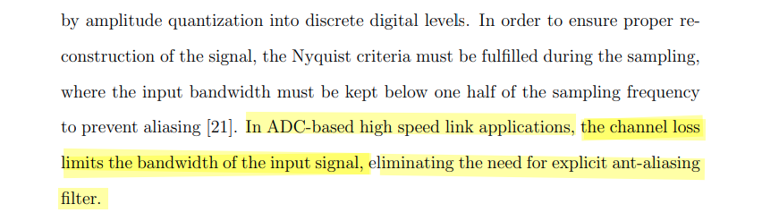
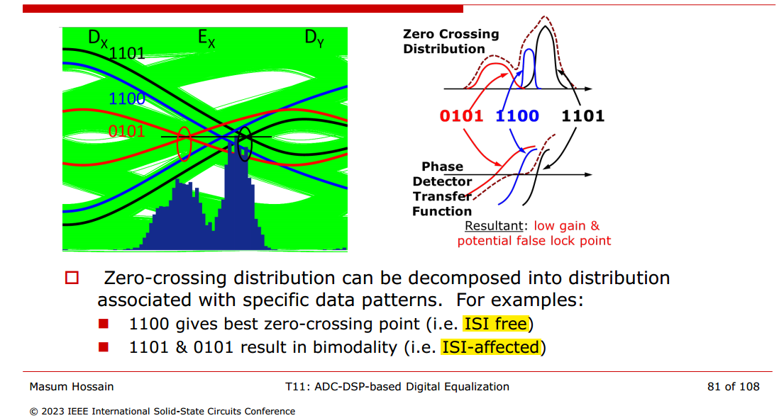
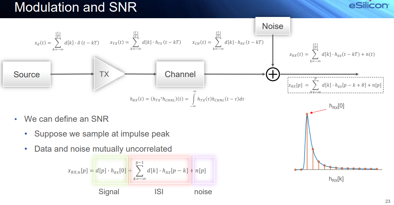
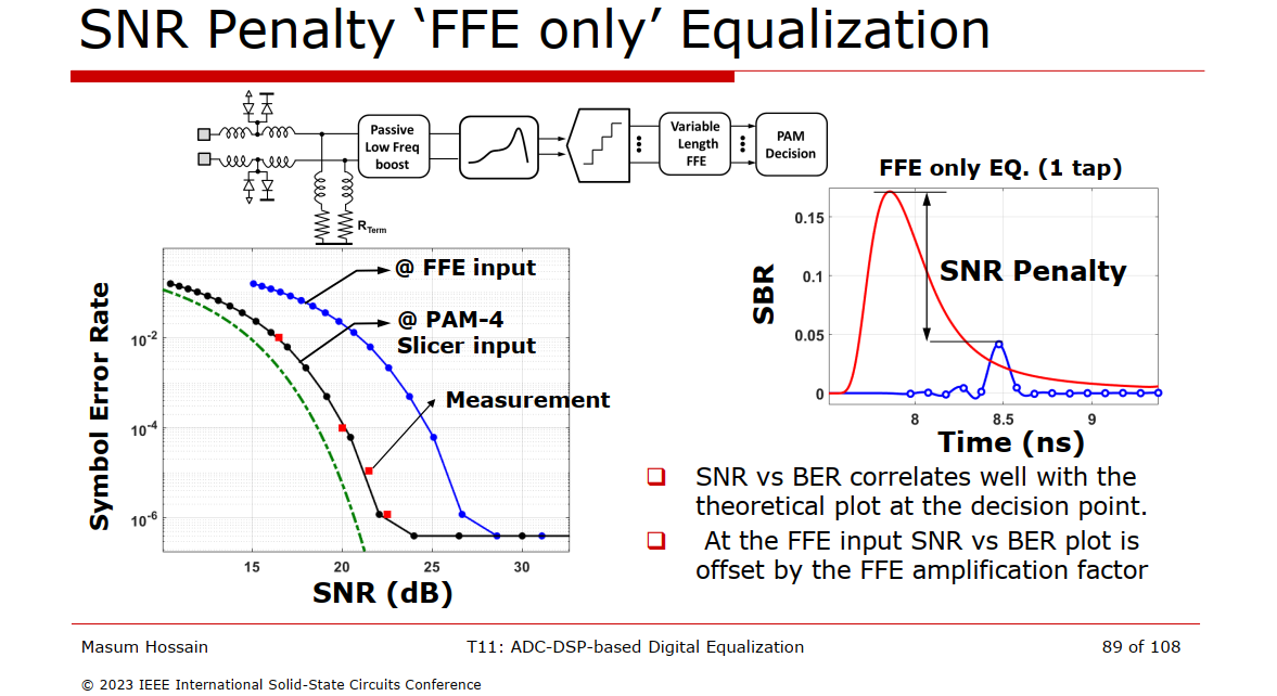

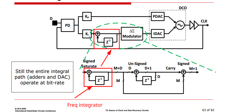
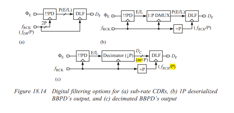
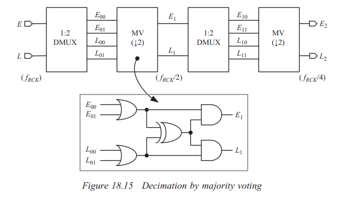

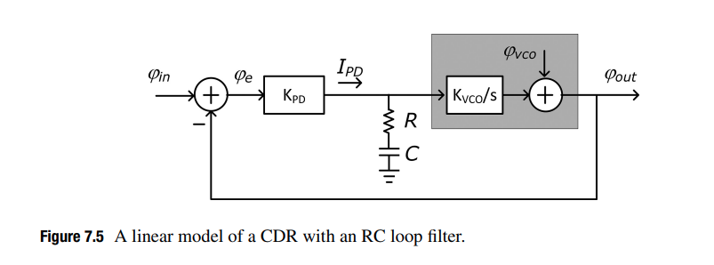
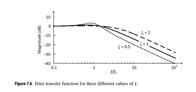
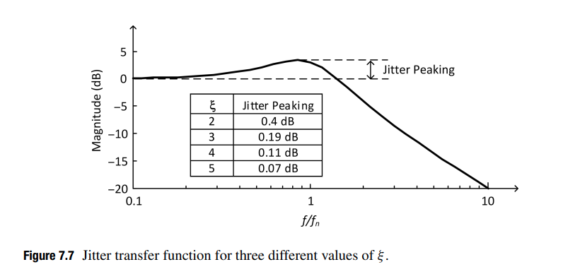
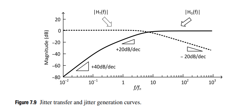
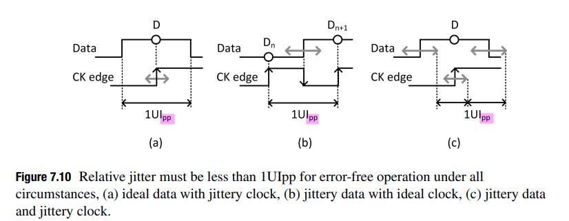
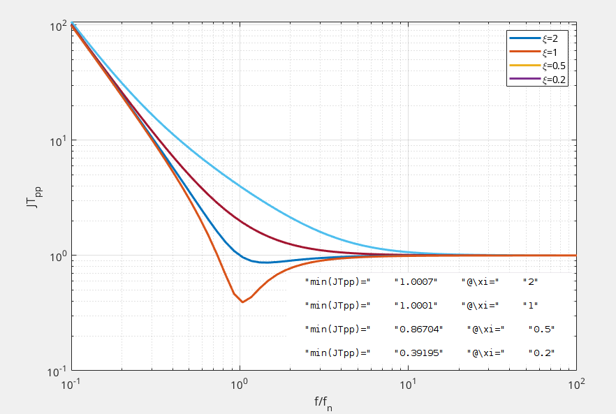
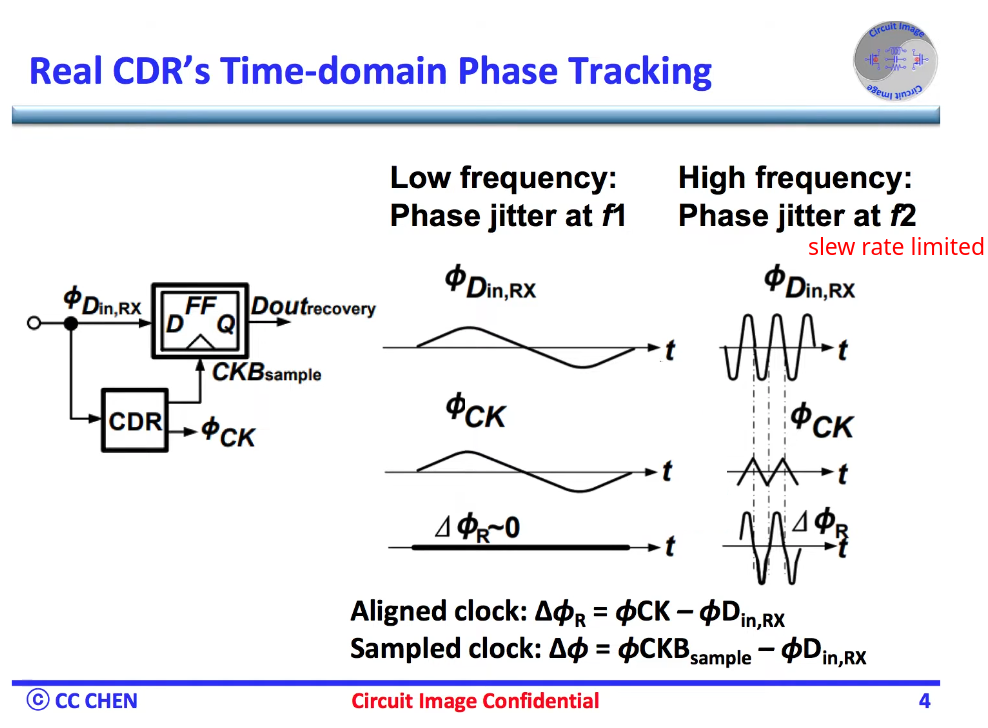
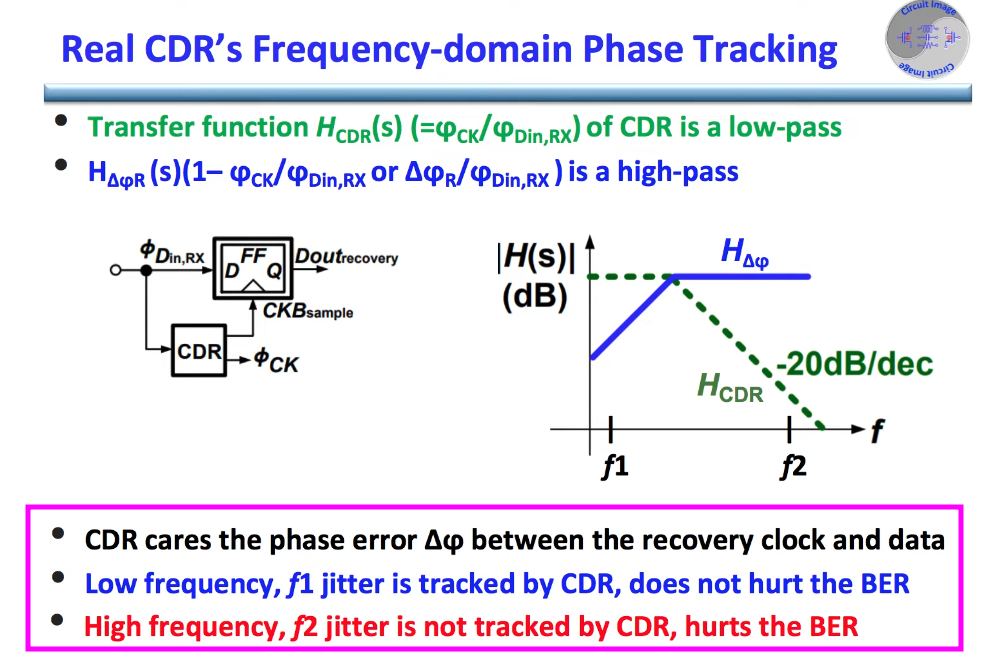
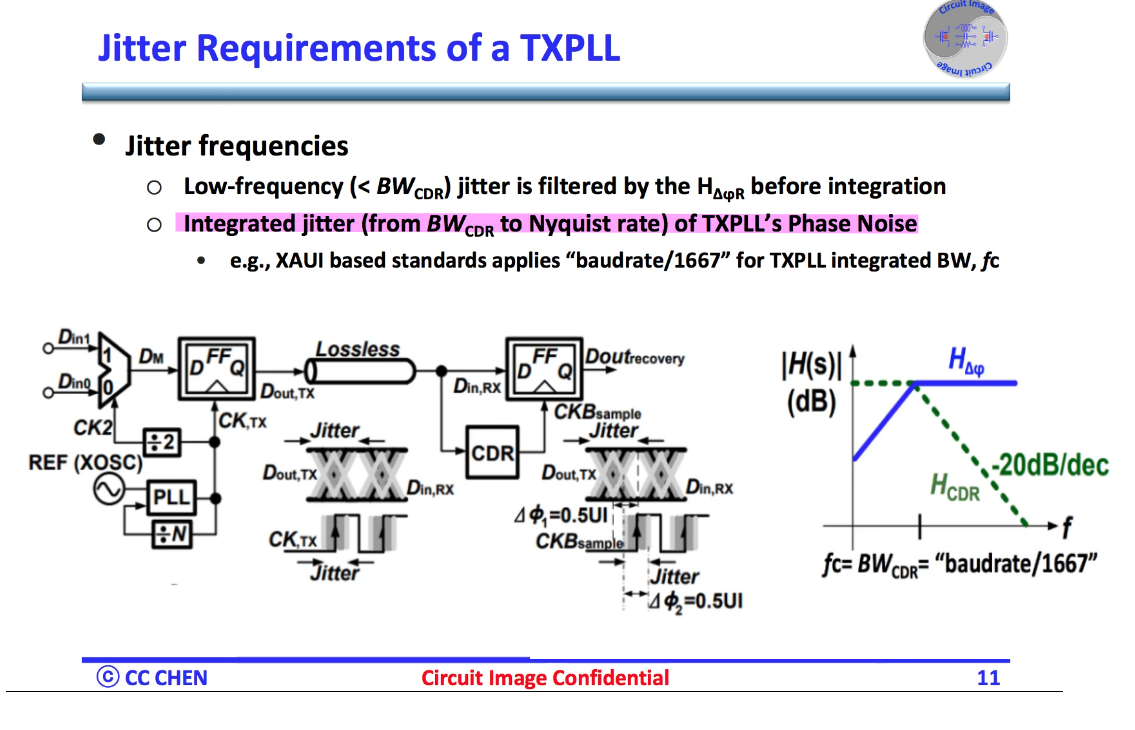
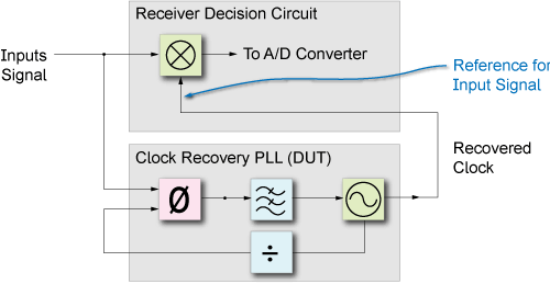
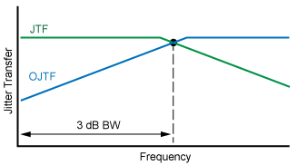
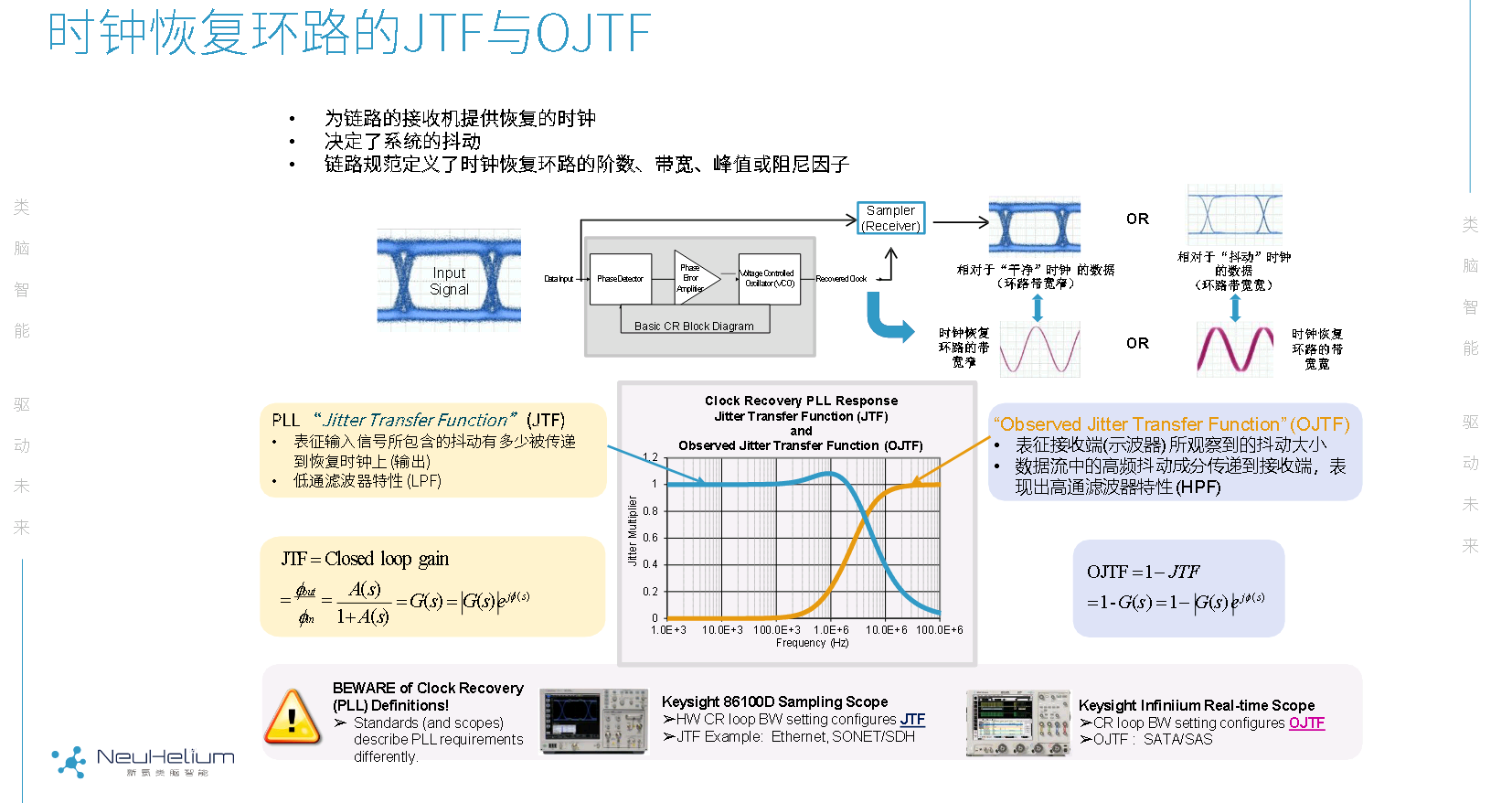
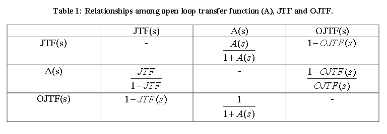
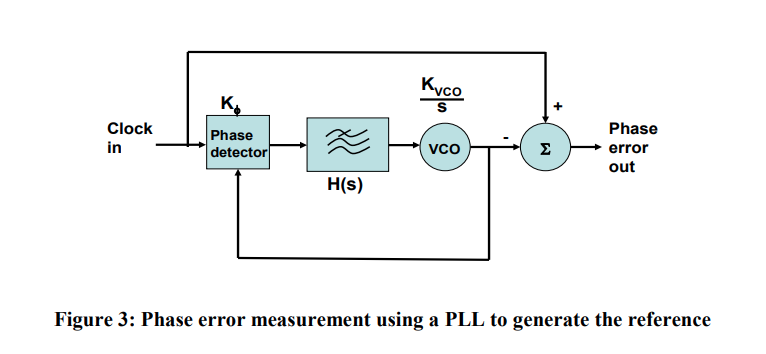
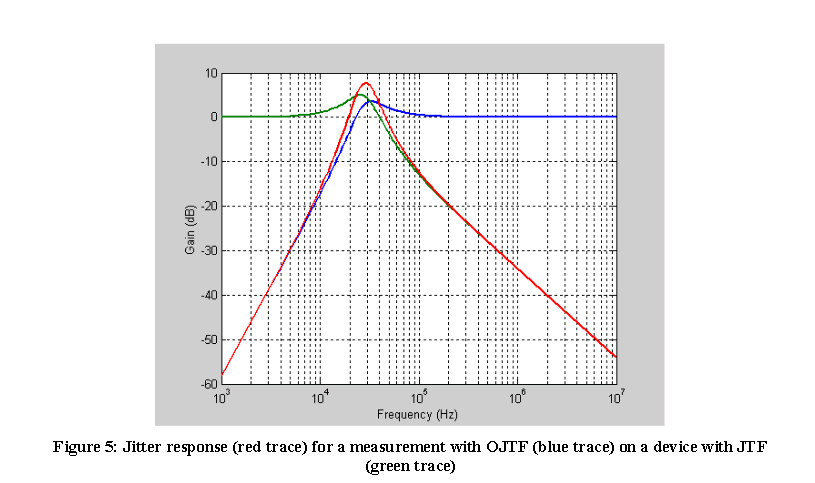
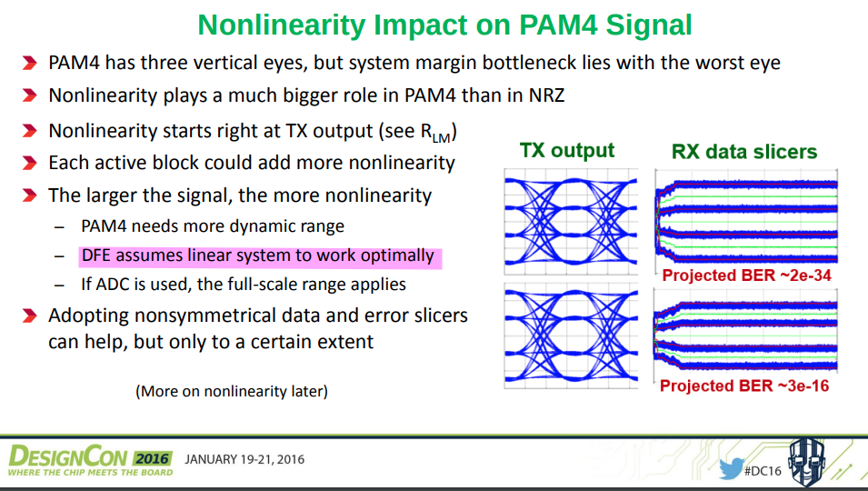
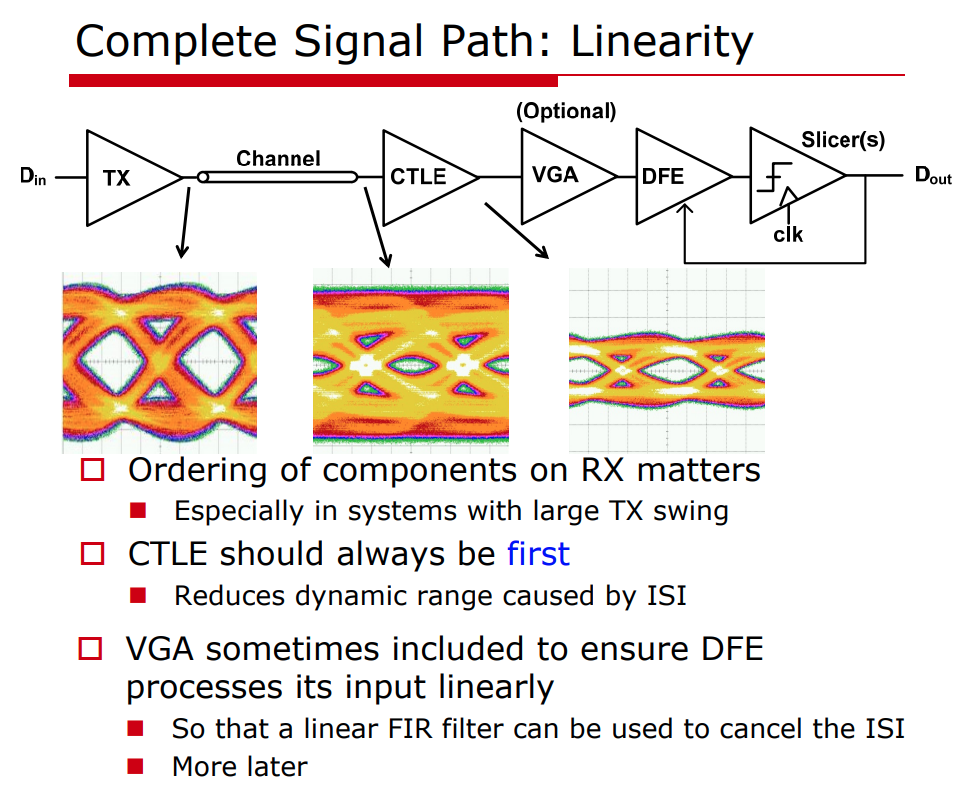
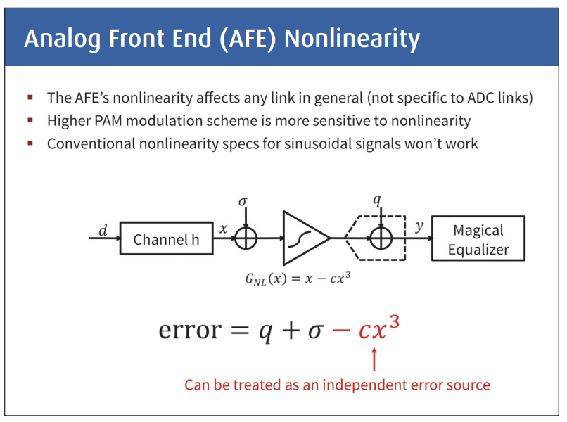
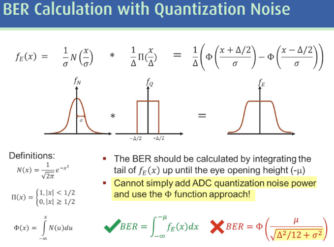
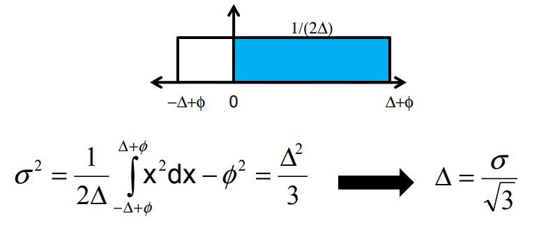
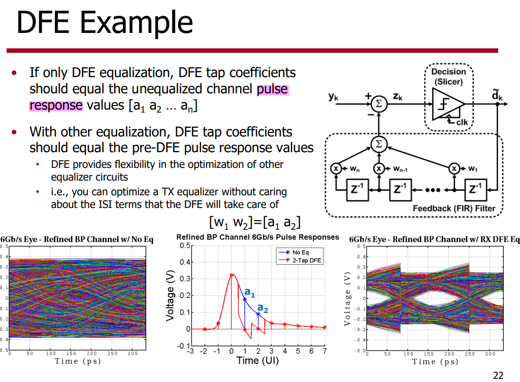
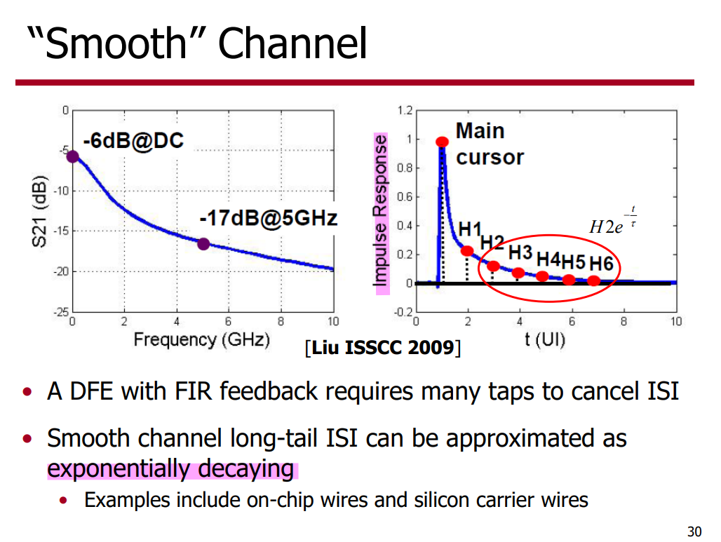
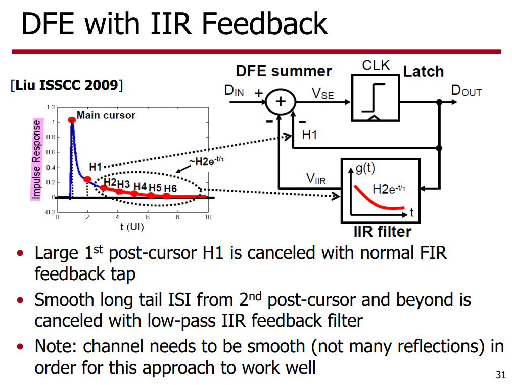
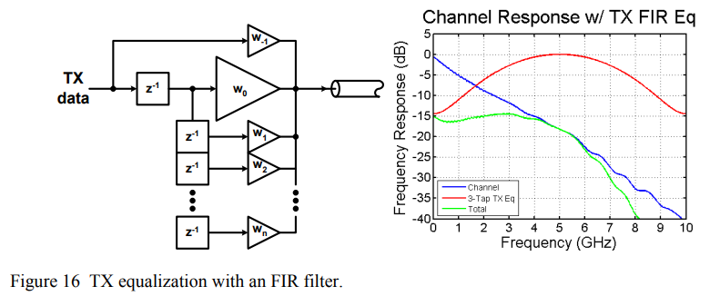
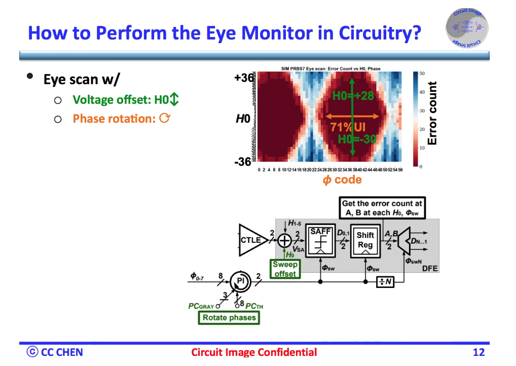
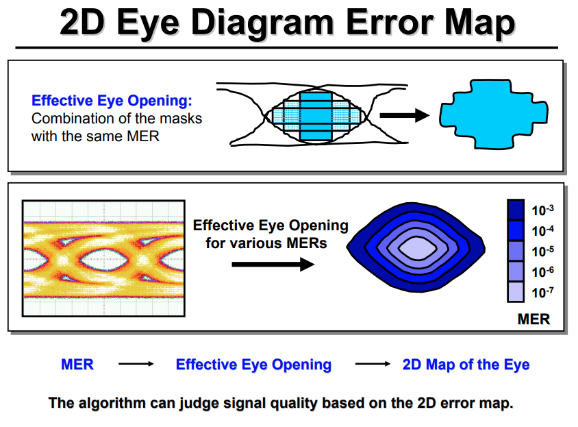

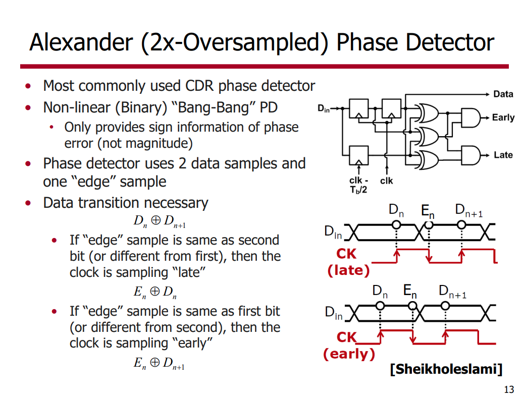
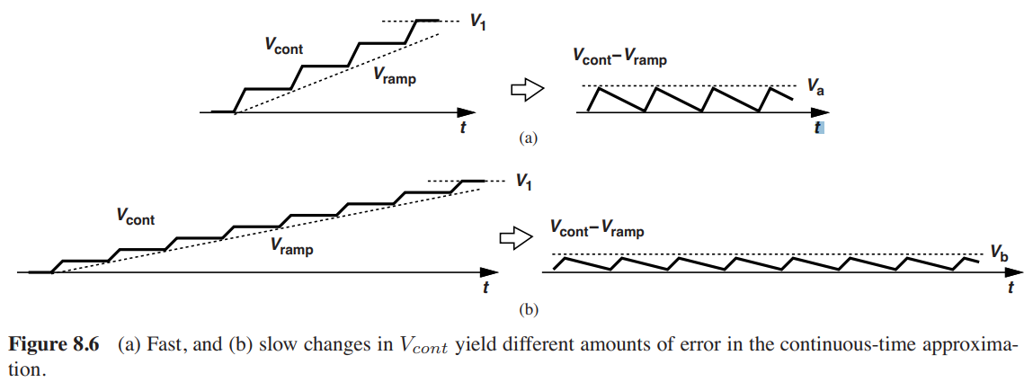
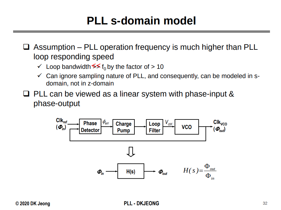
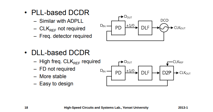
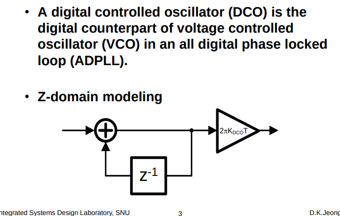
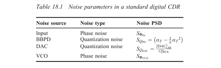
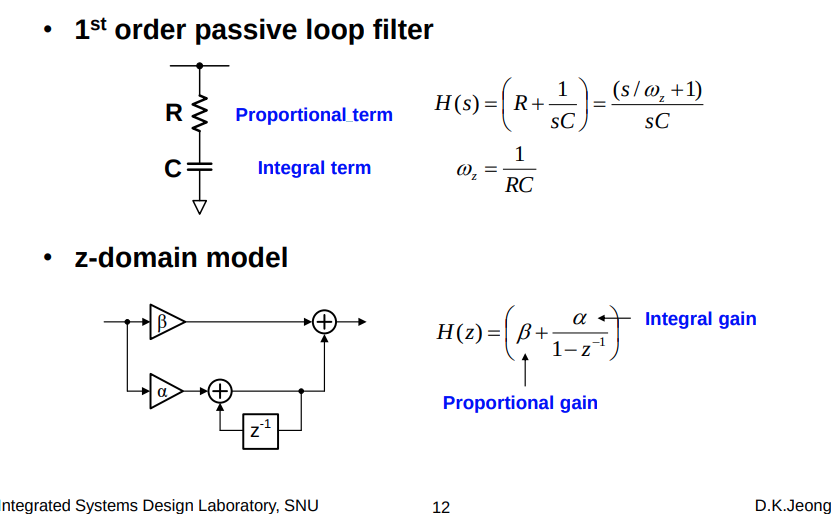
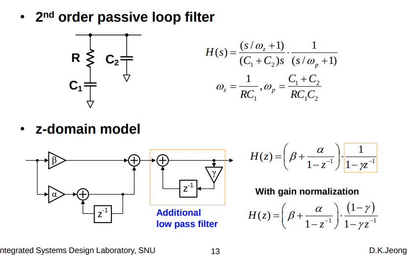
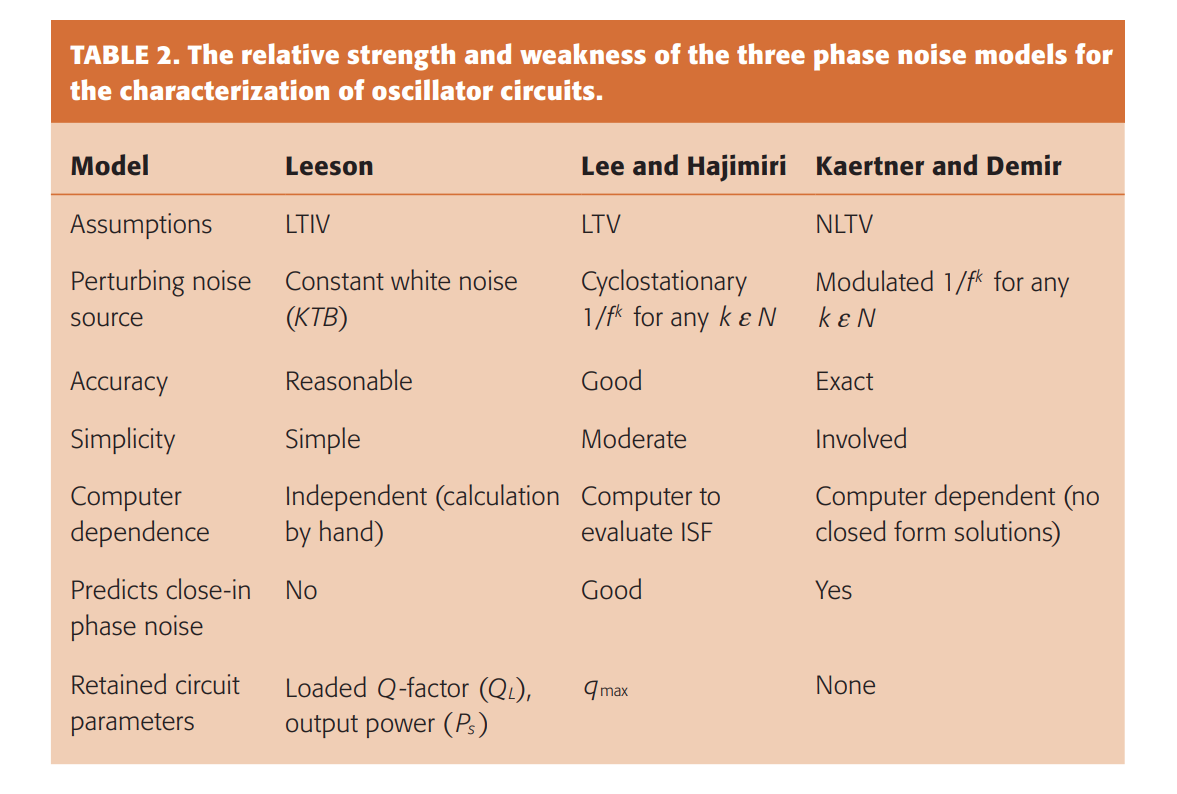
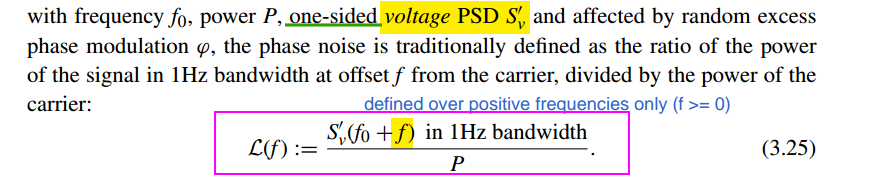
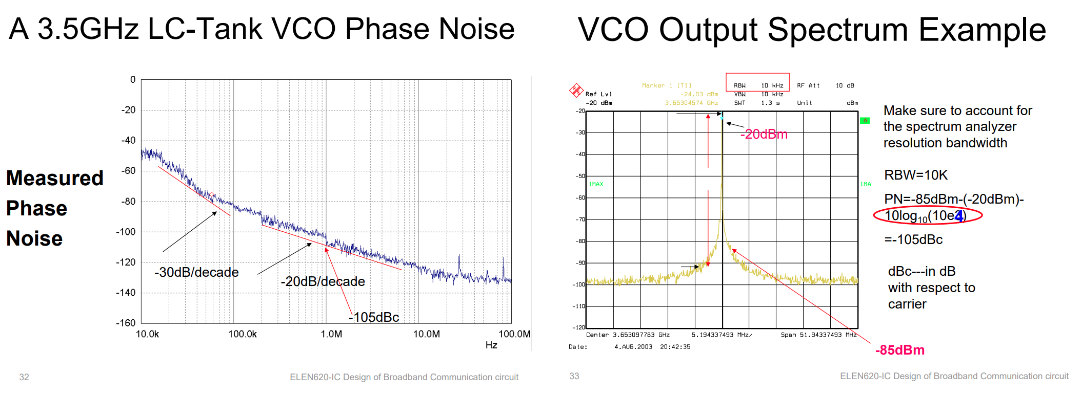
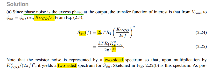
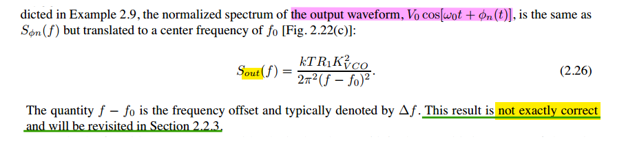
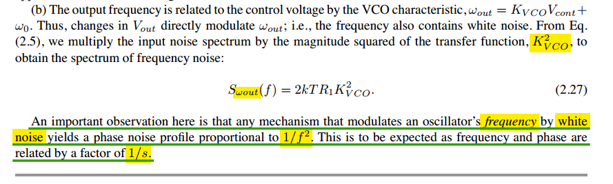
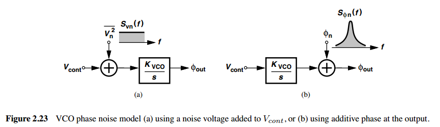
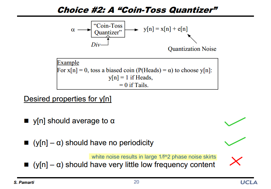
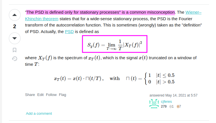
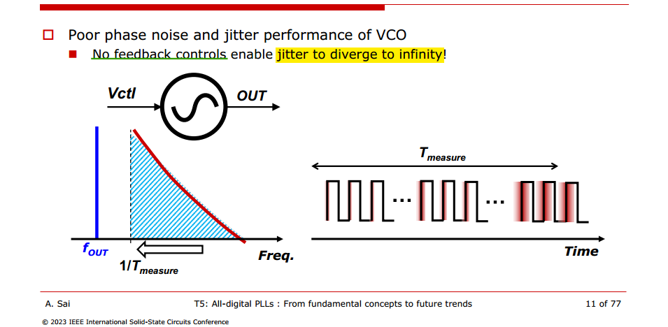
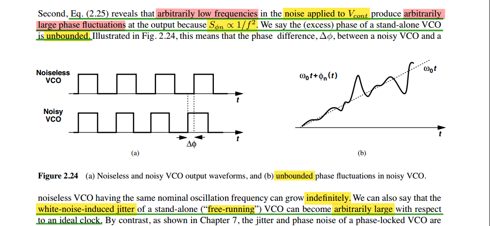
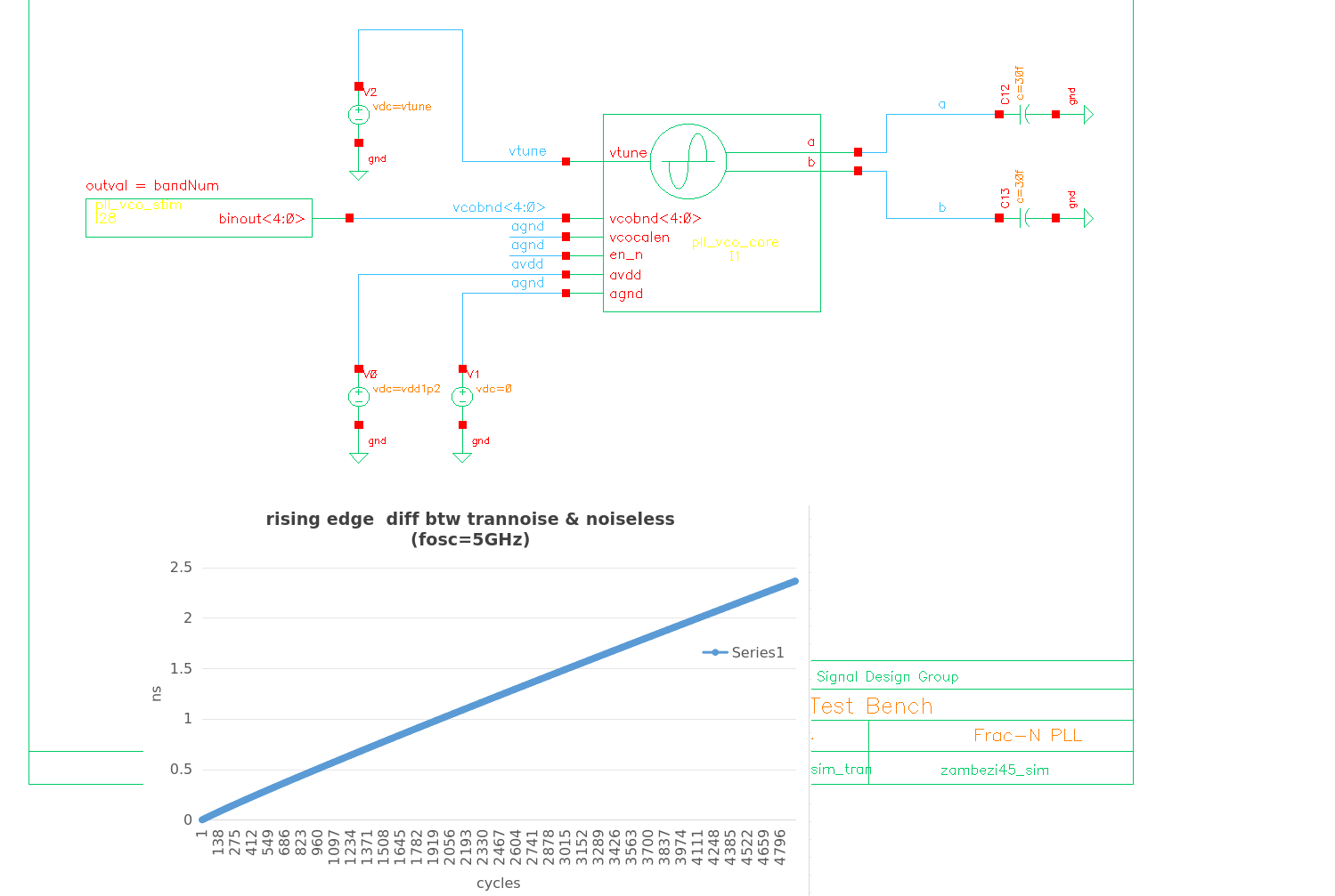
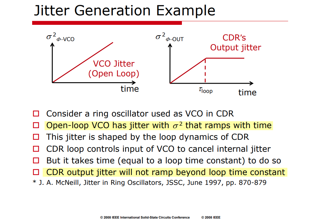
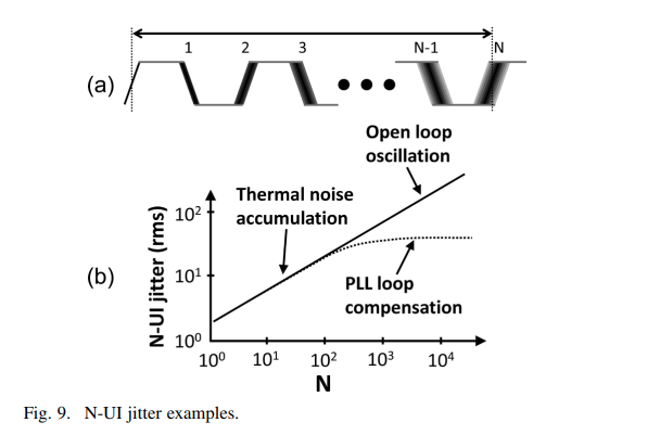
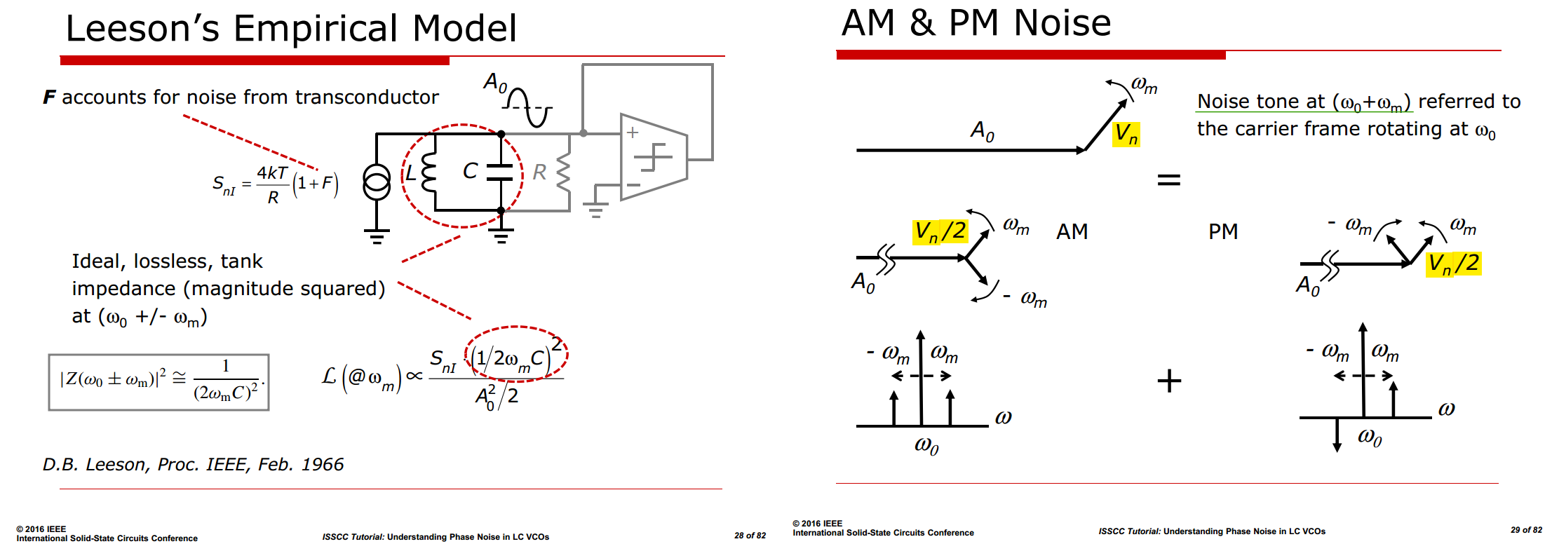
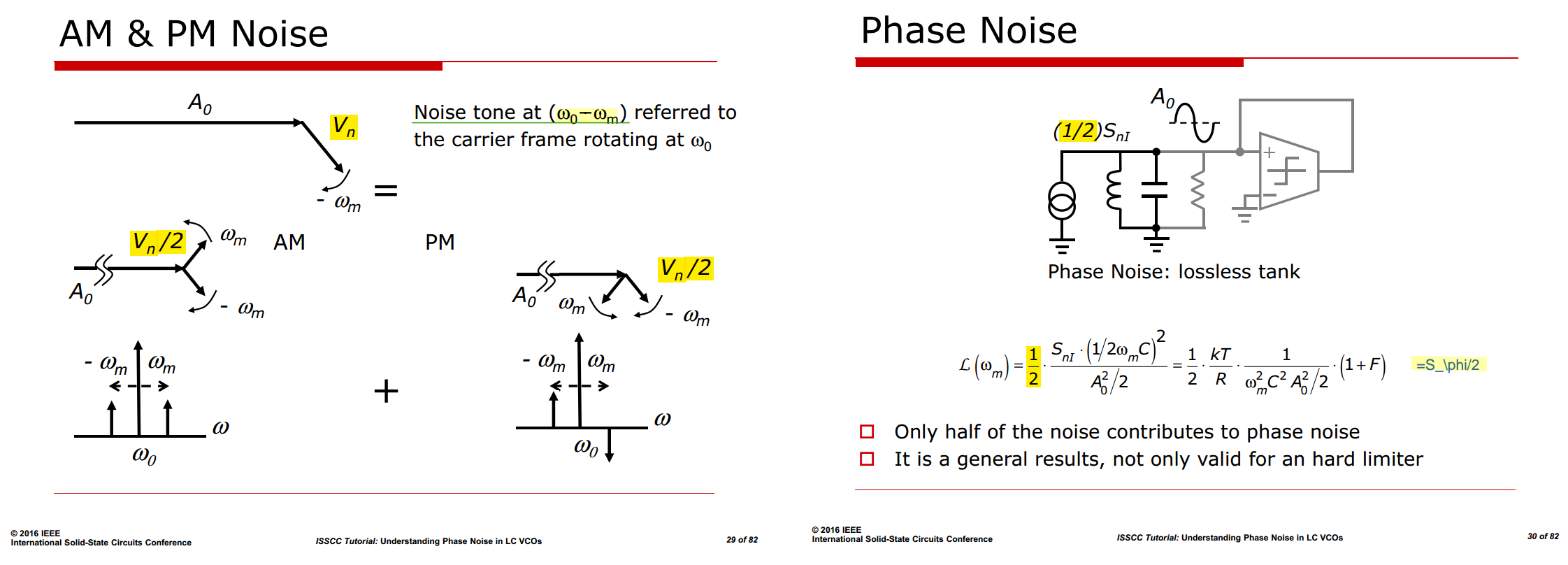

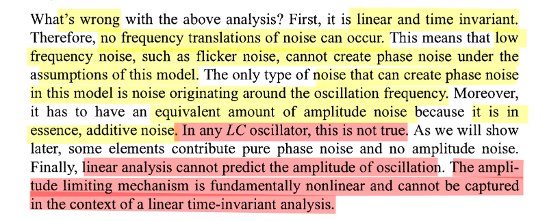
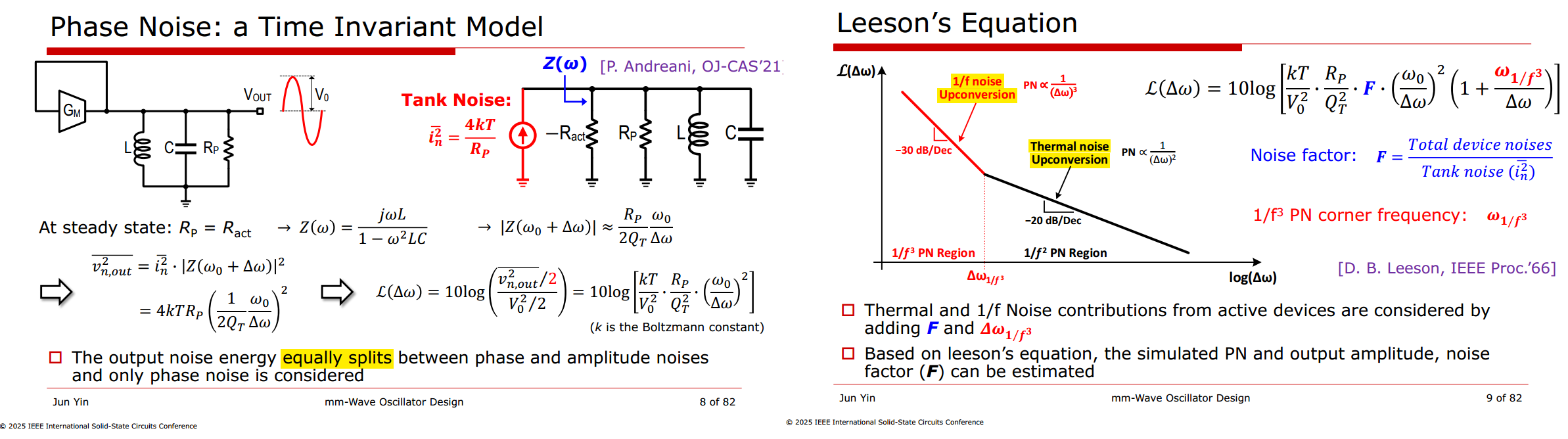
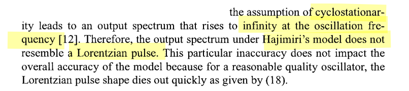
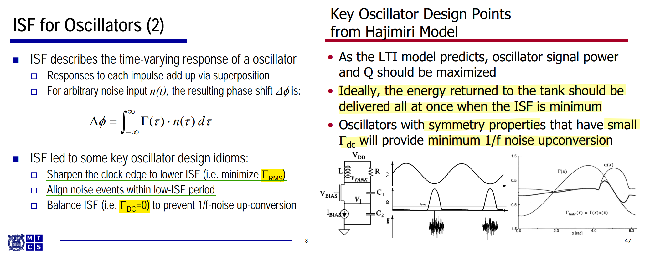
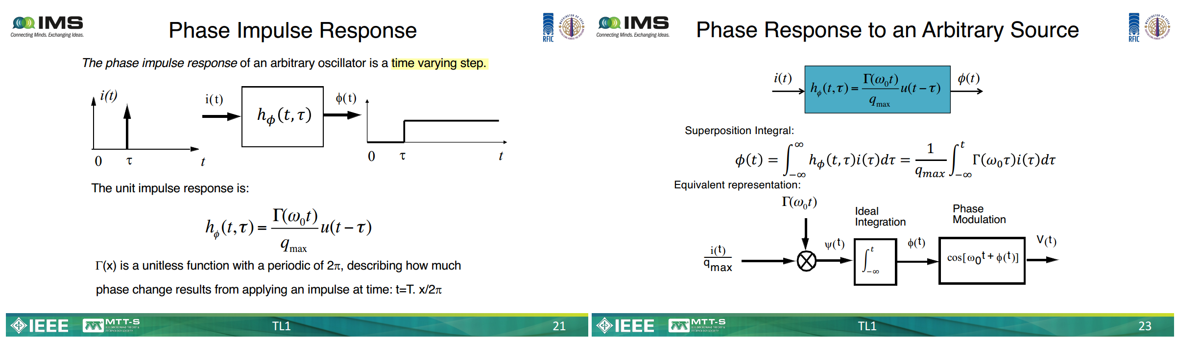
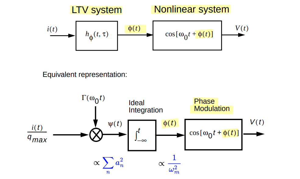
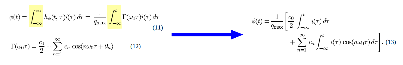
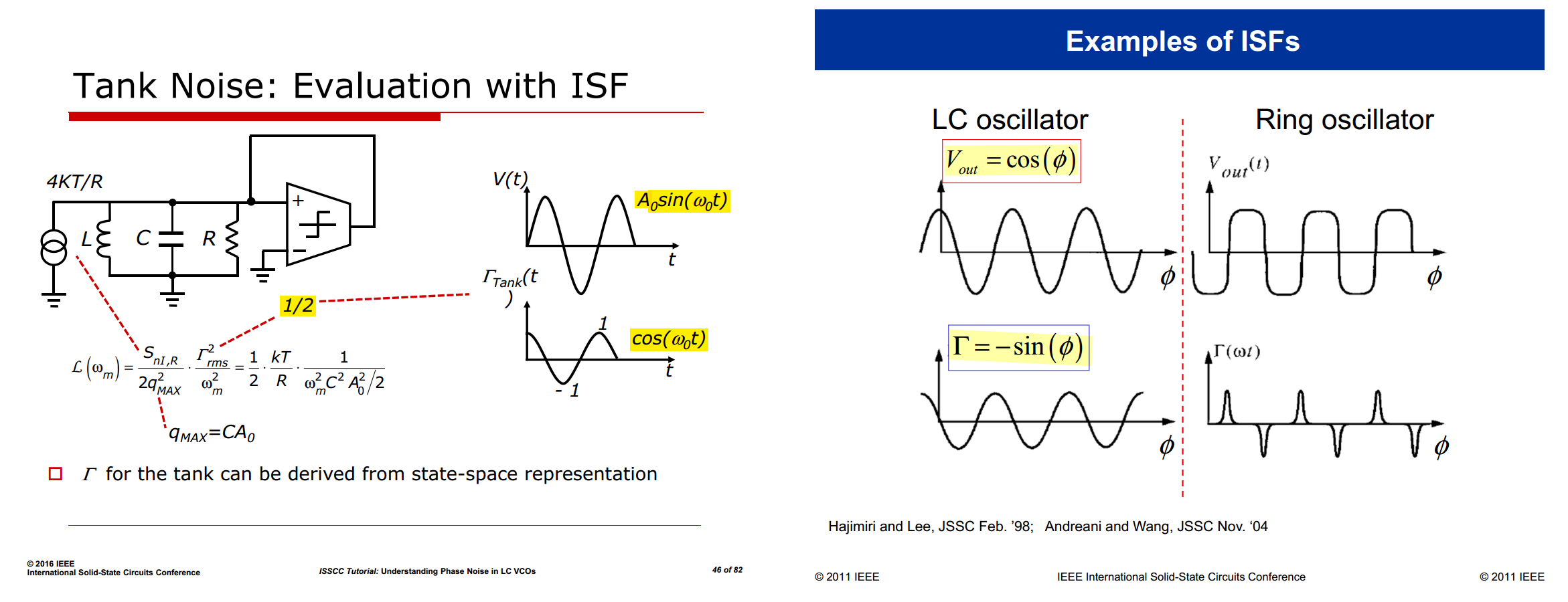
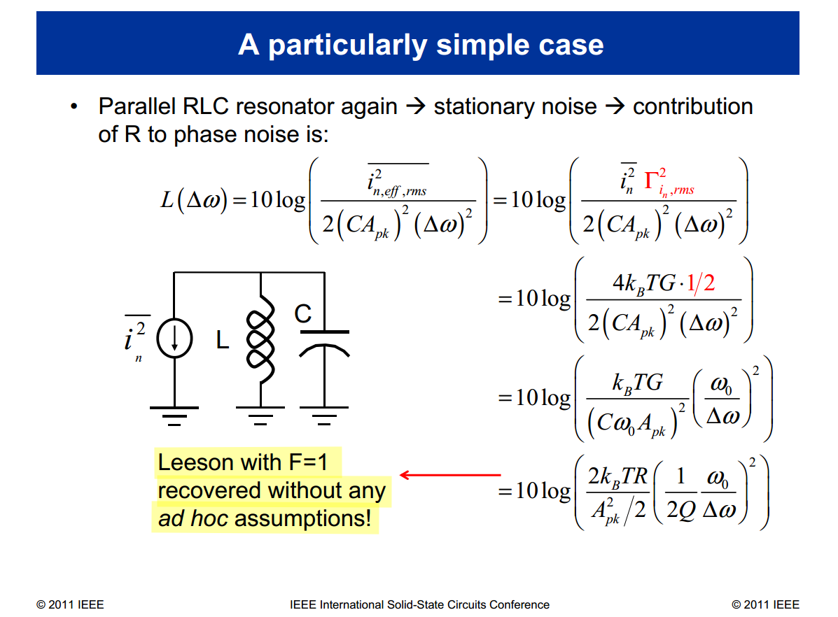
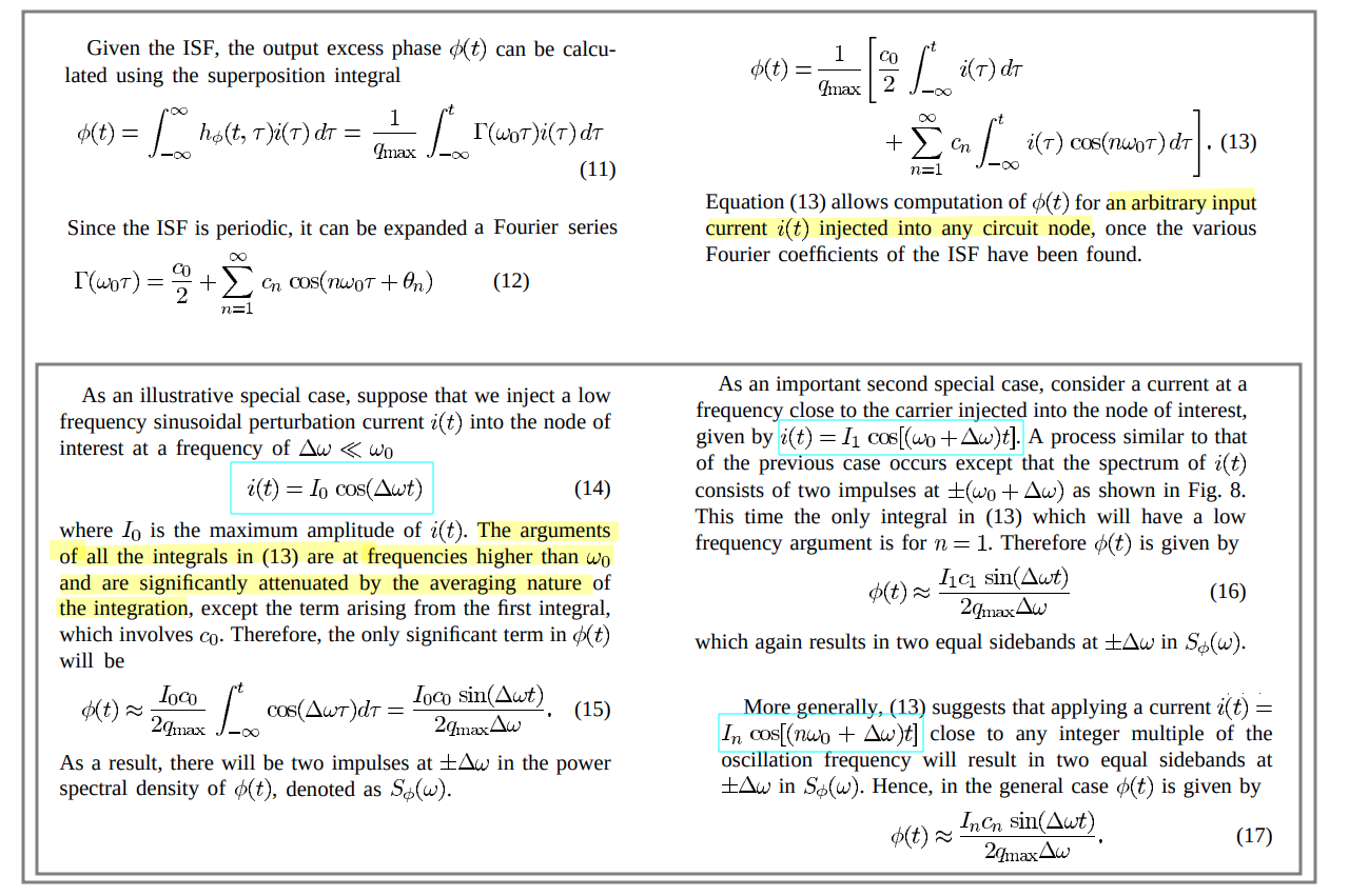
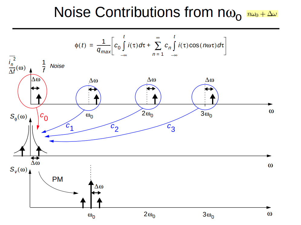
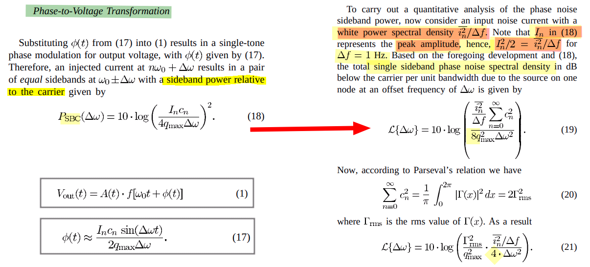
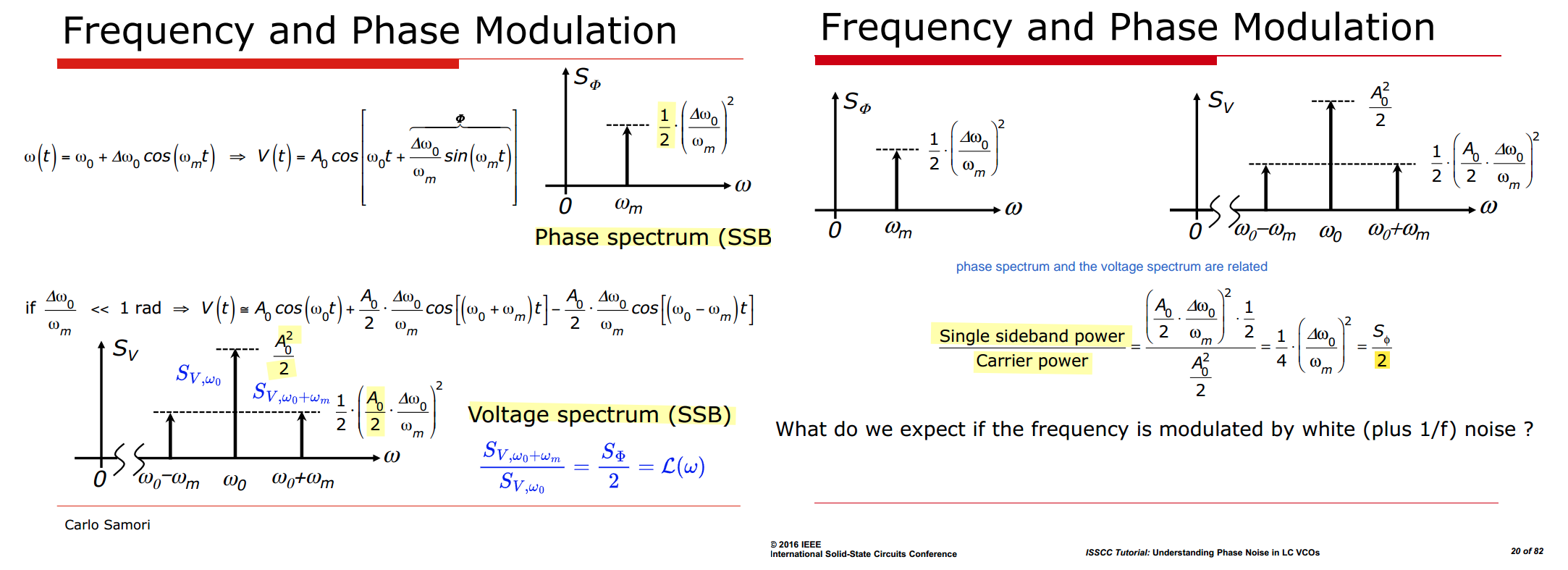
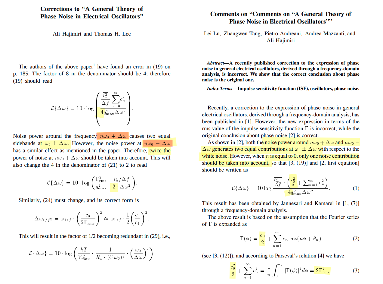
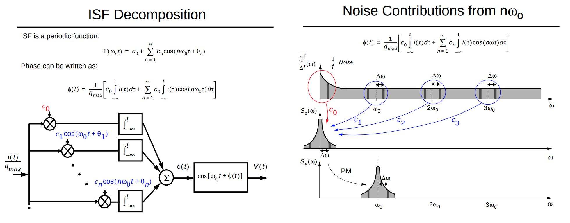
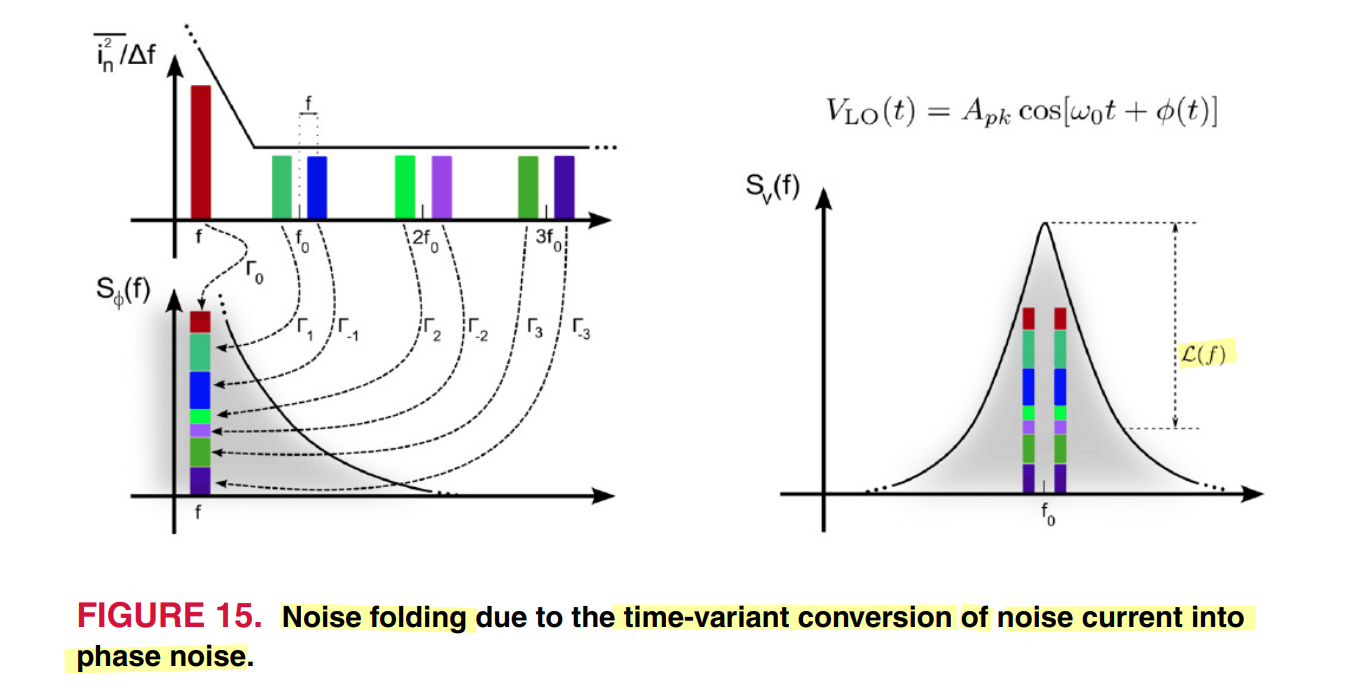
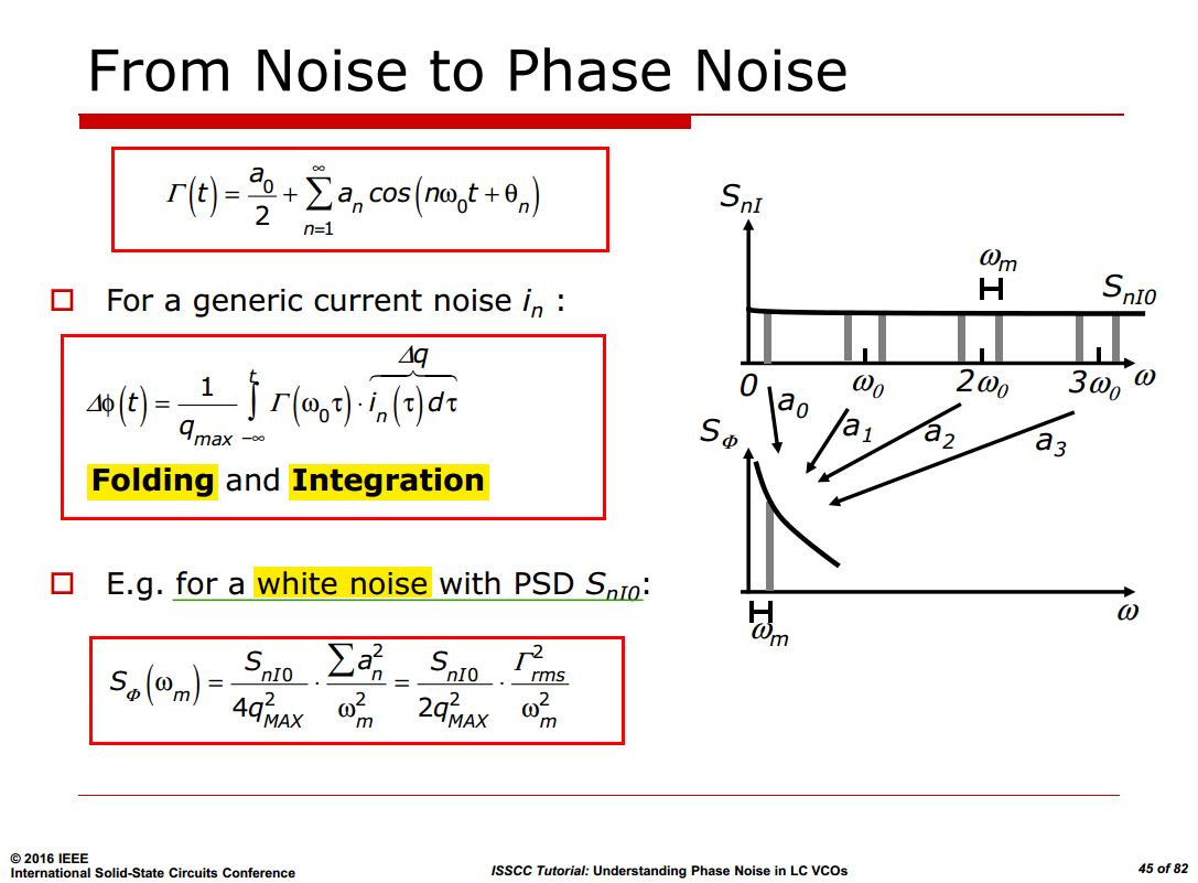
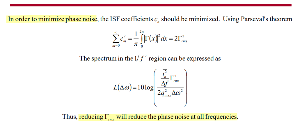
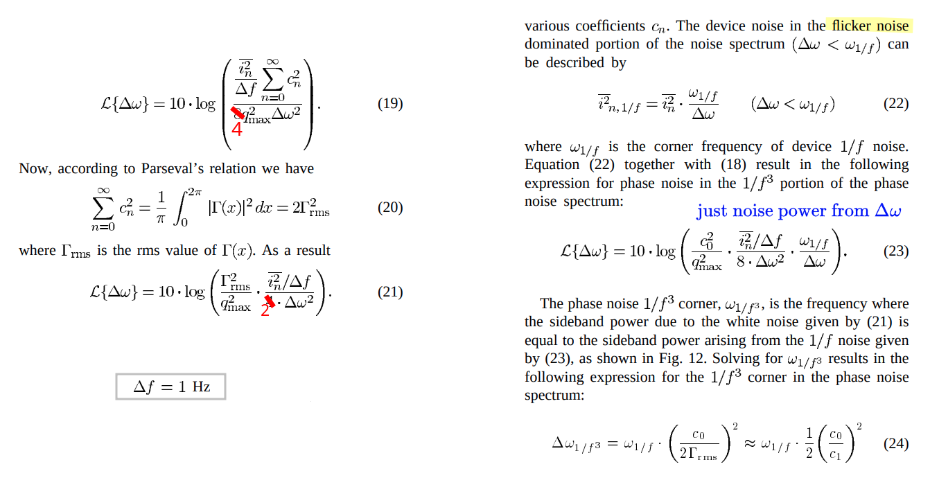
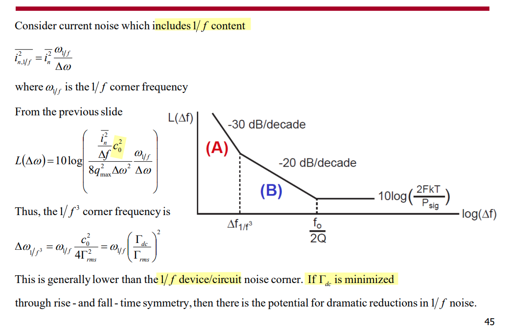
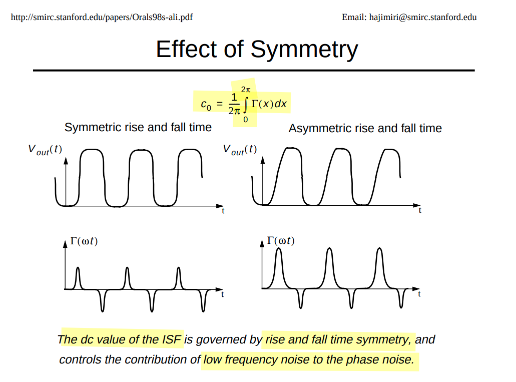
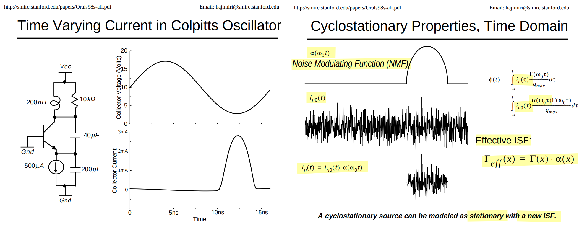
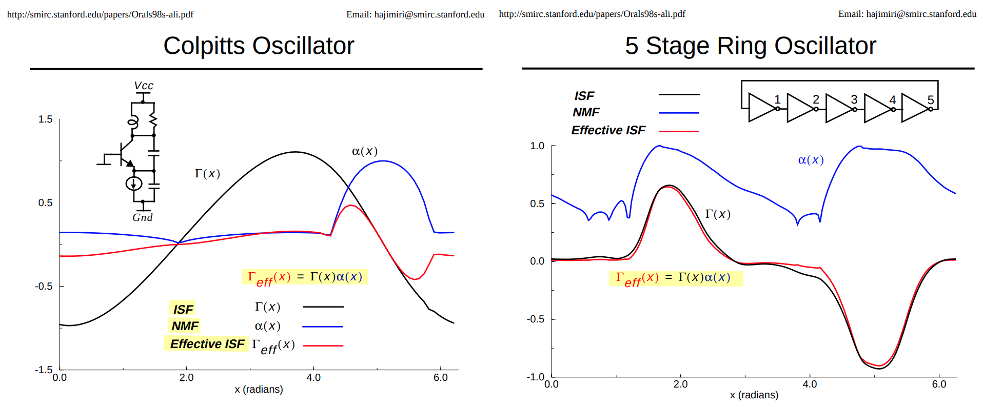
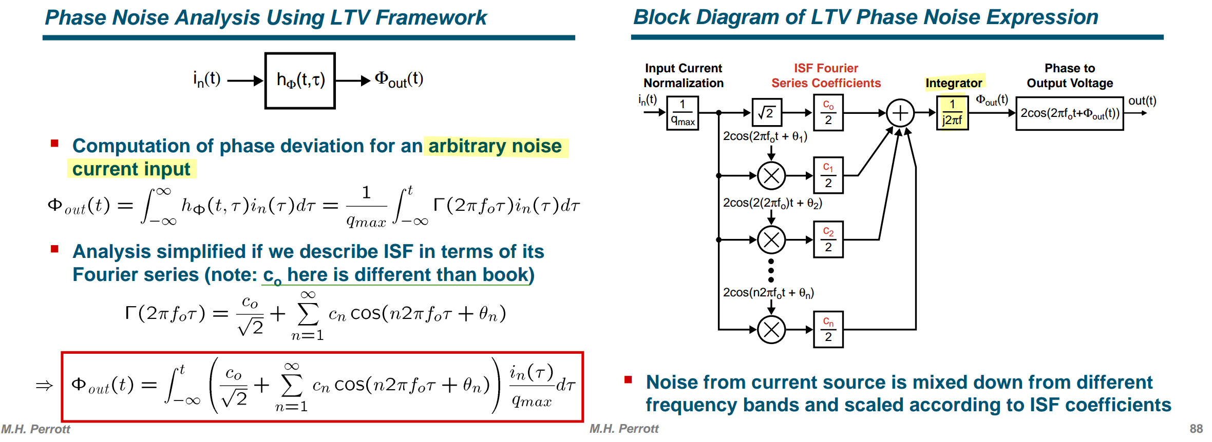
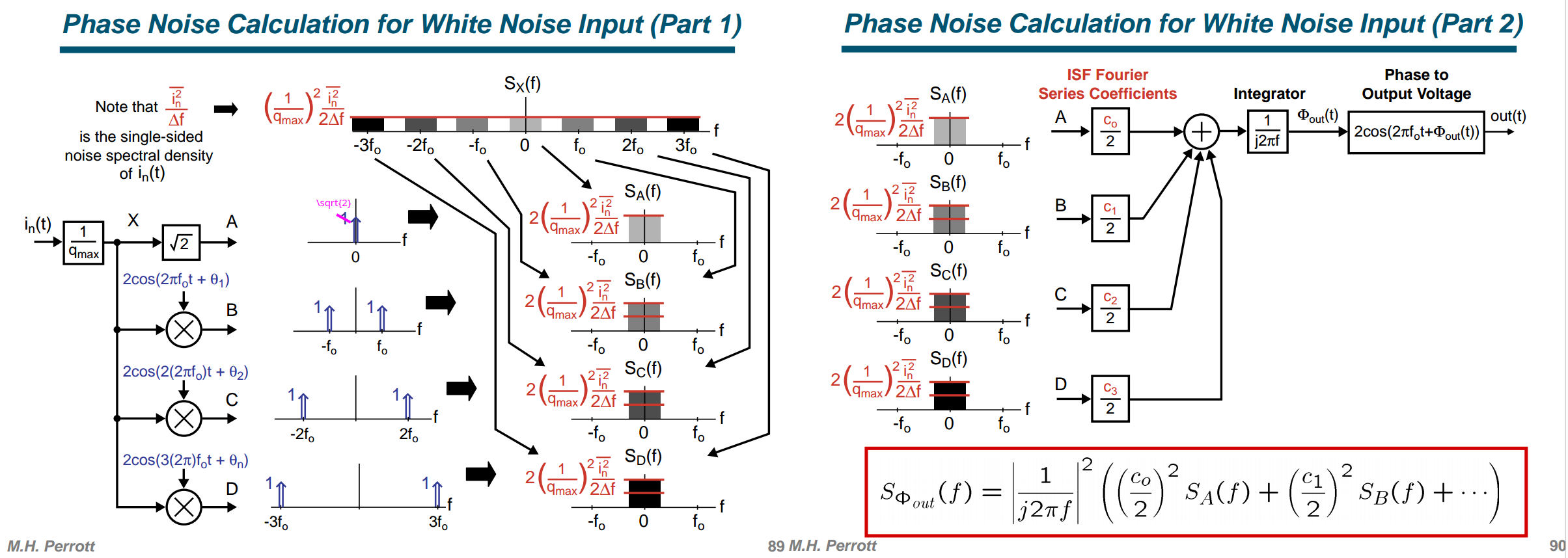
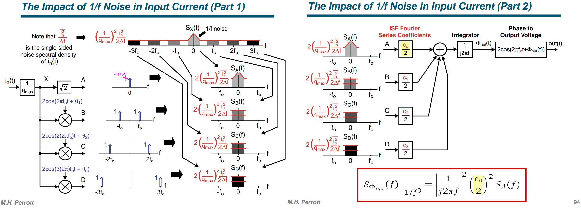
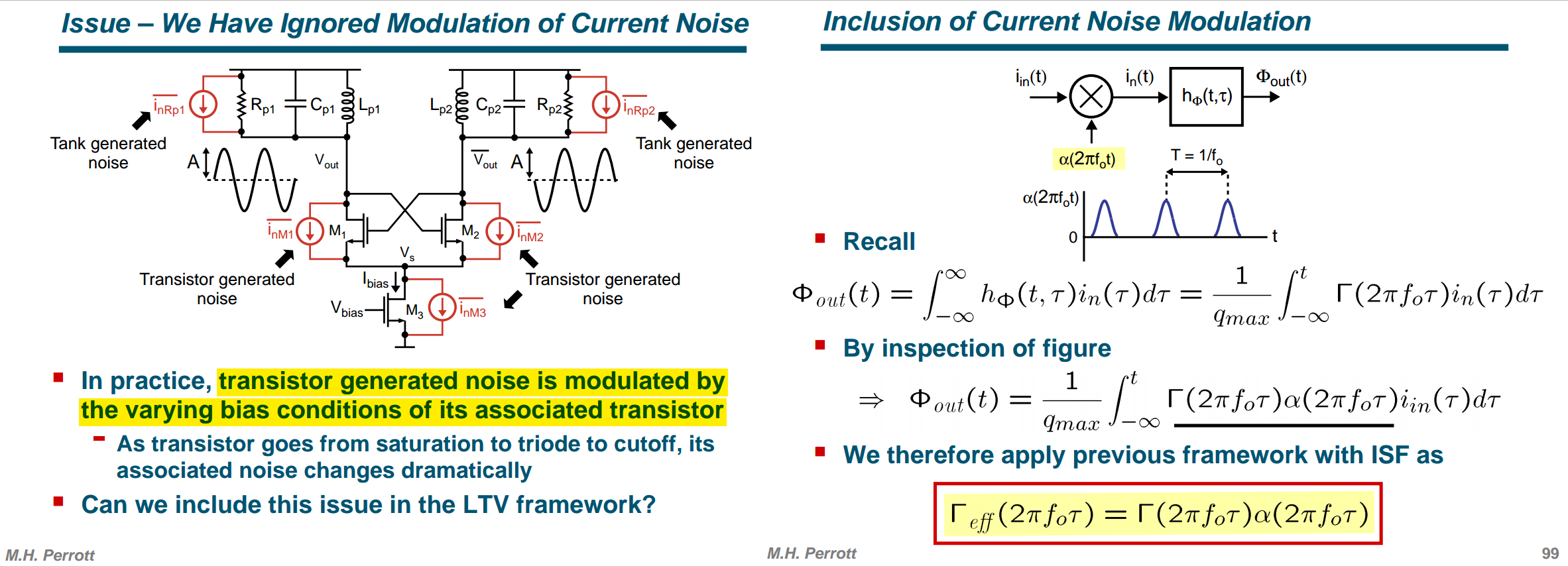
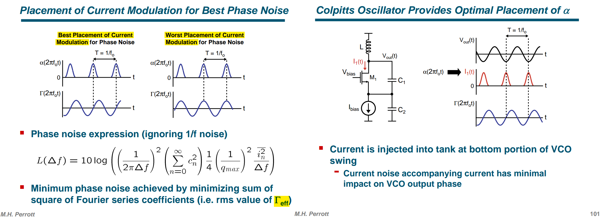
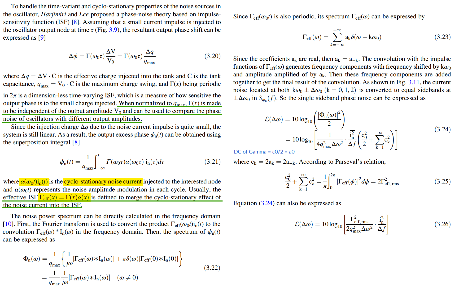
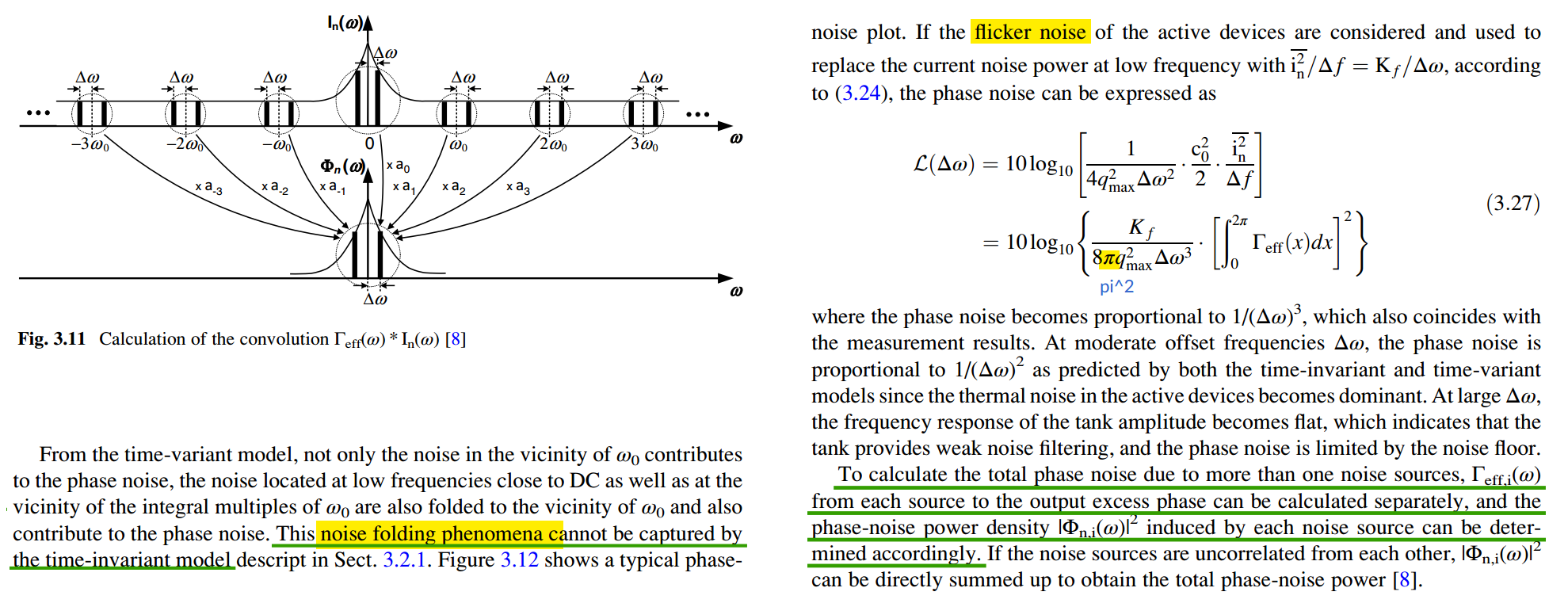

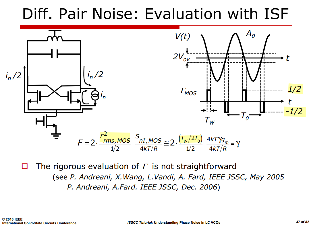

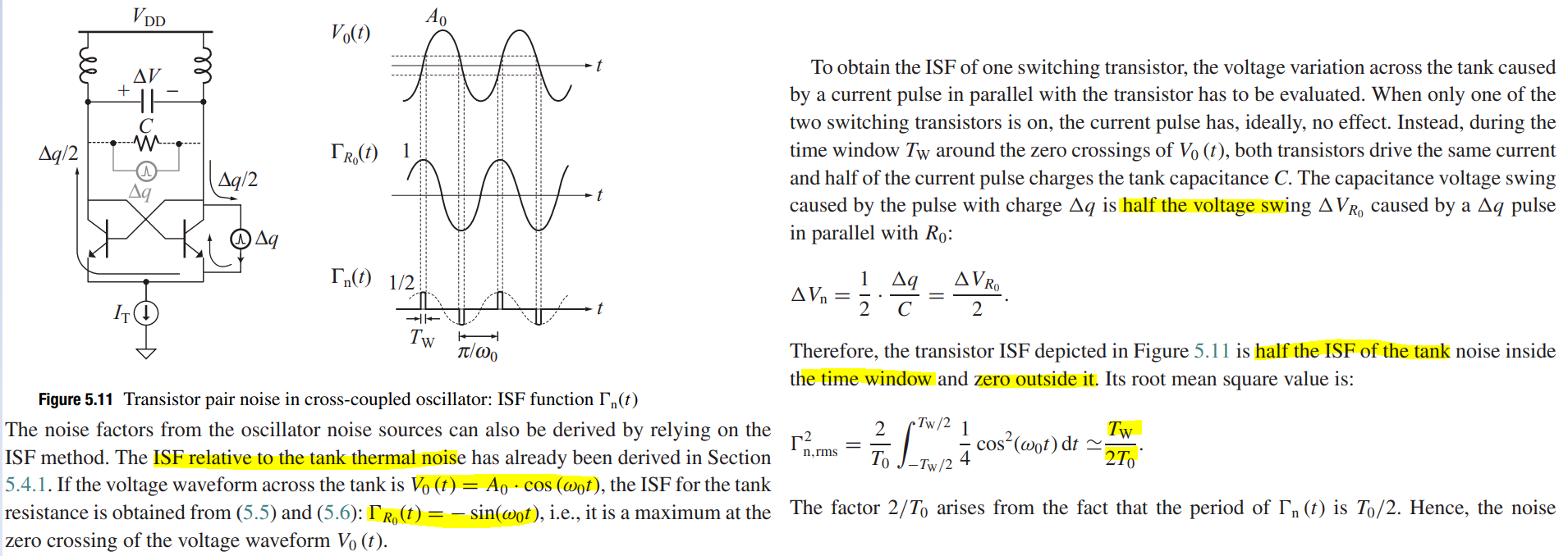
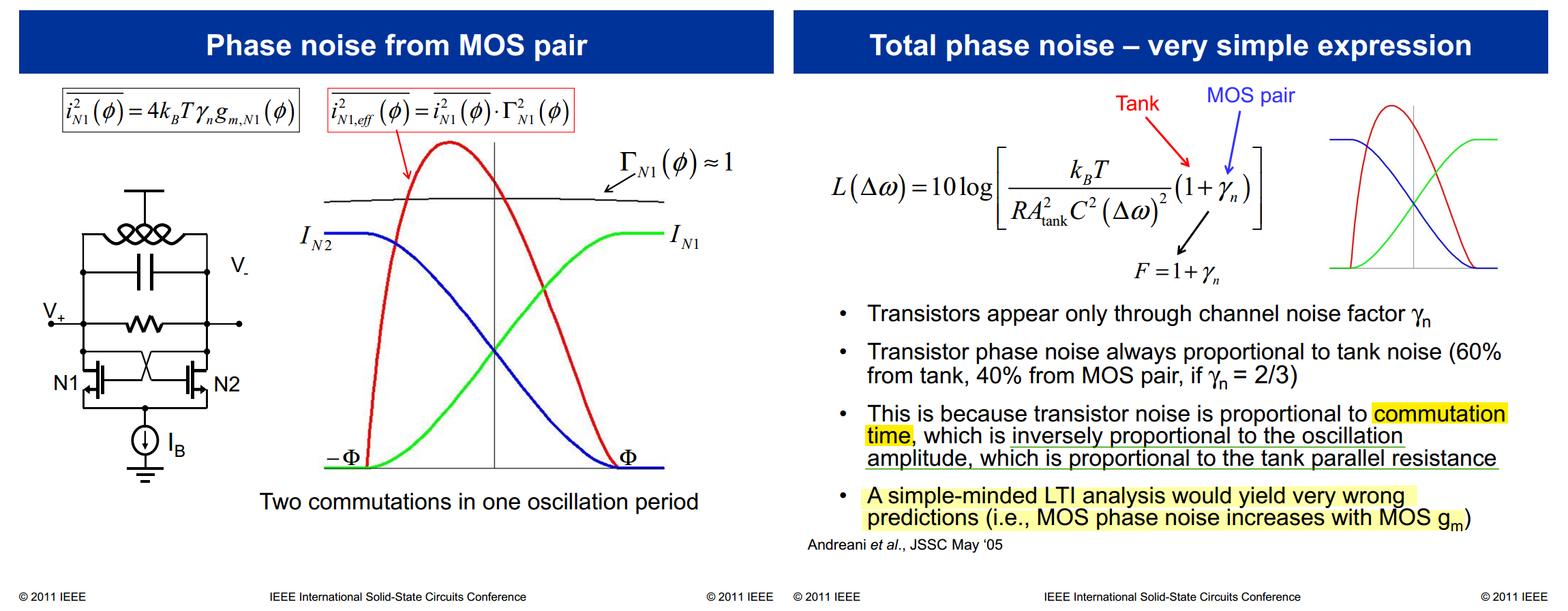
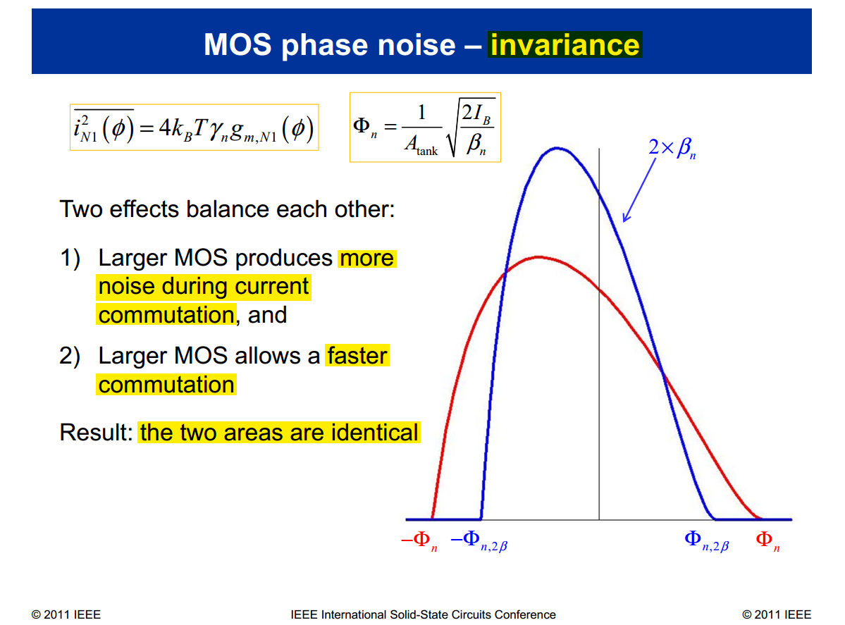
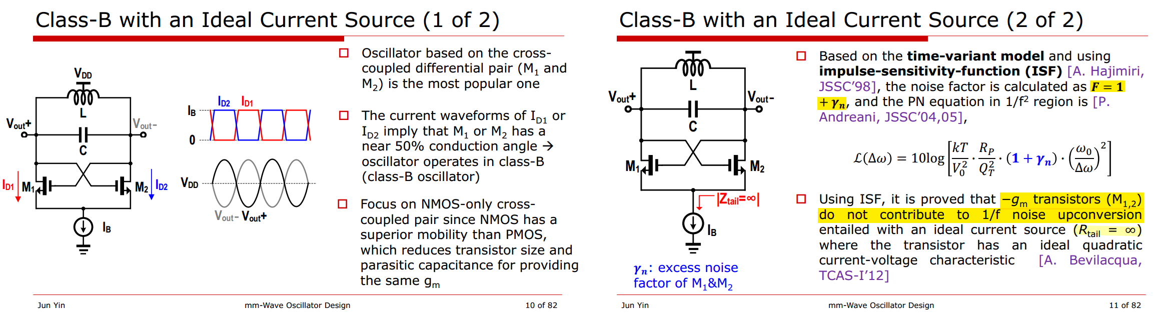

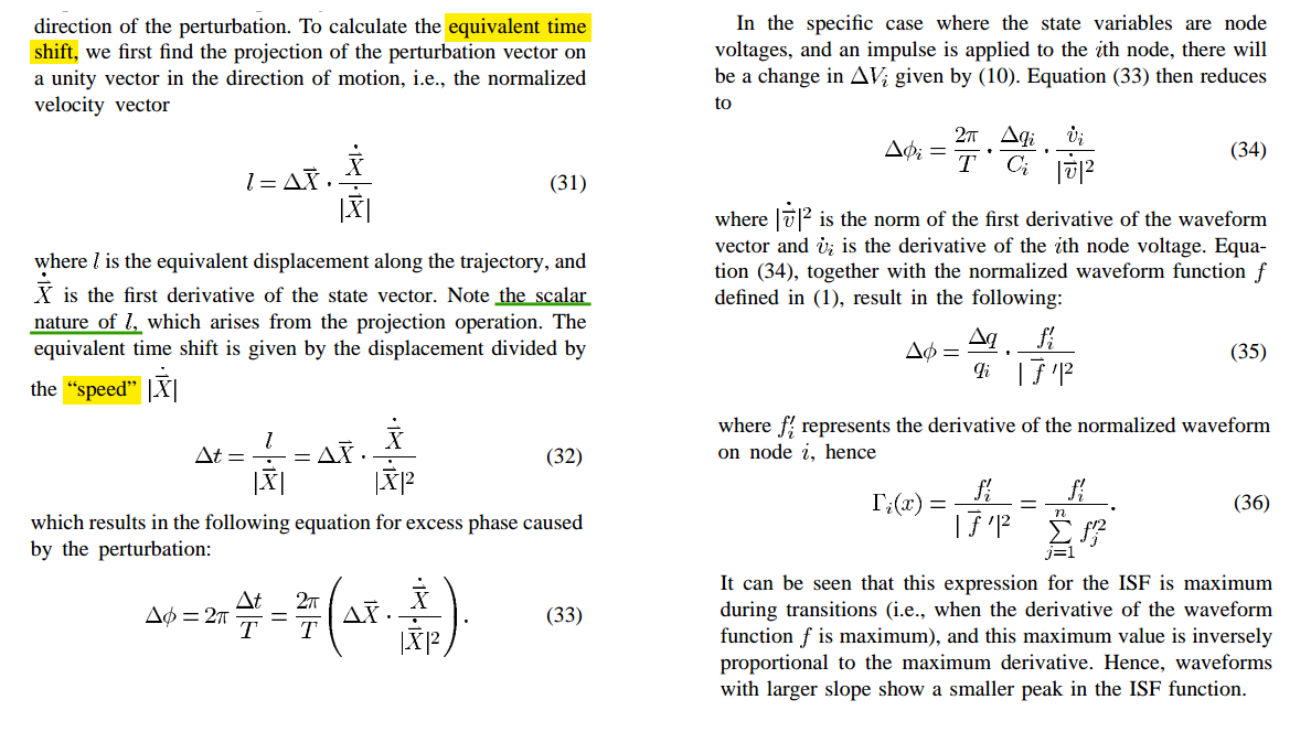 If the state variables are node
voltages, write
If the state variables are node
voltages, write