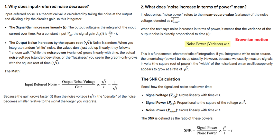
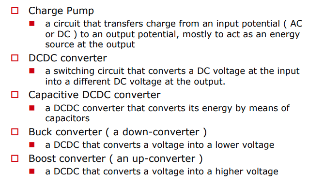
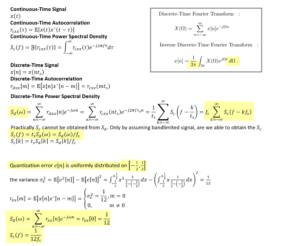
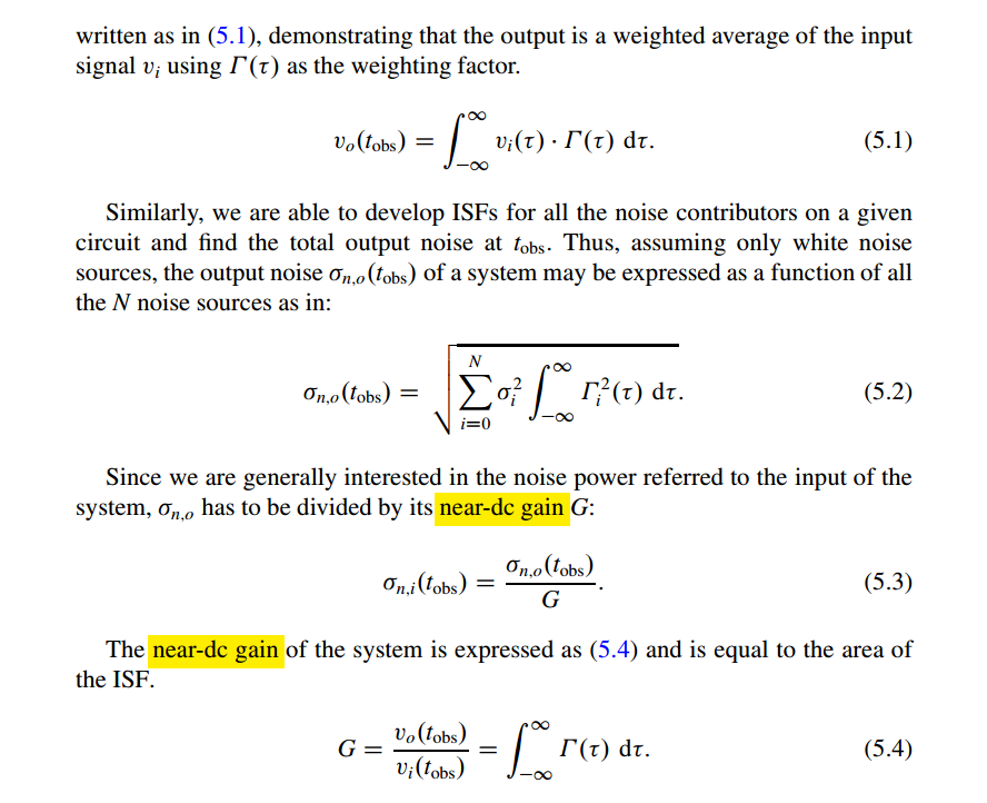
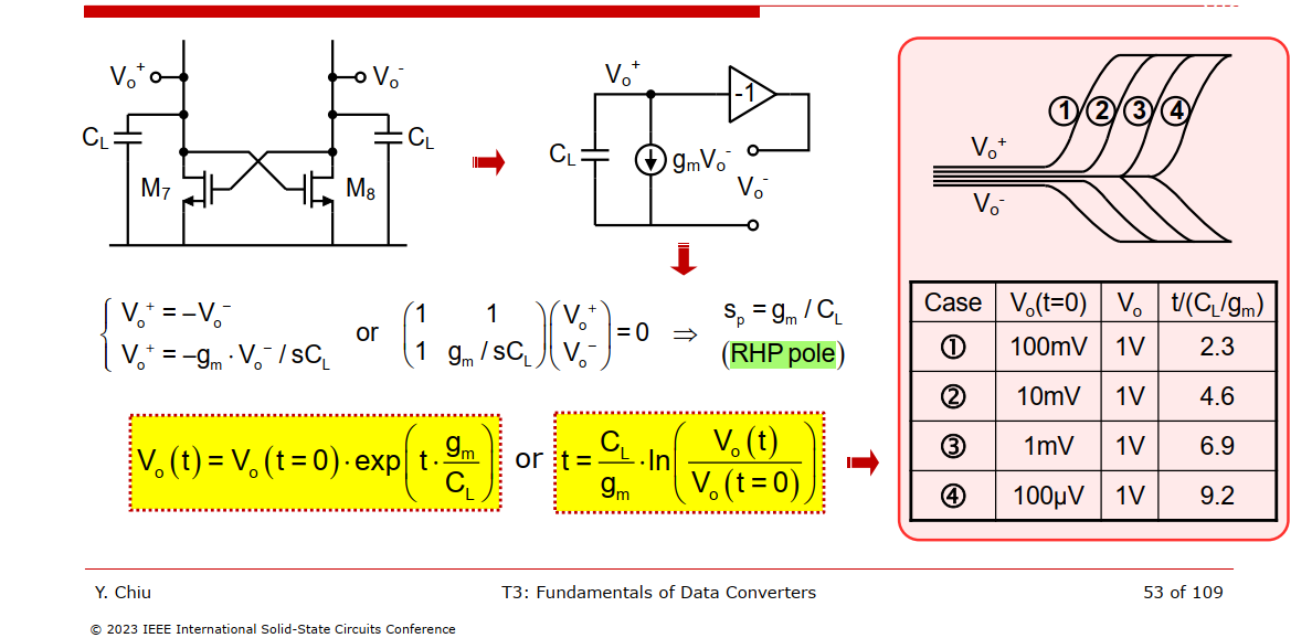
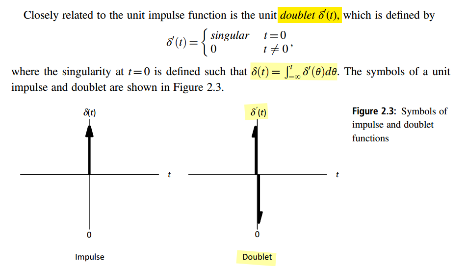
charge pumps are capacitive
DC-DC converters. The two most common switched capacitor
voltage converters are the voltage inverter and the
voltage doubler circuit
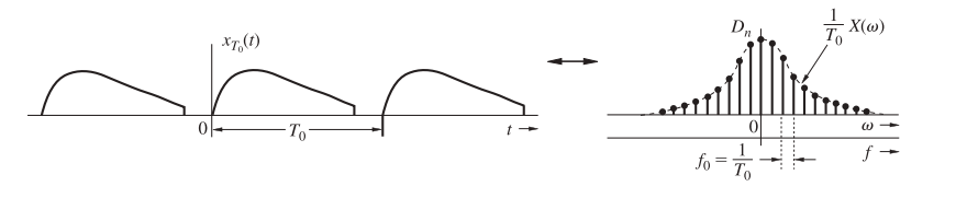
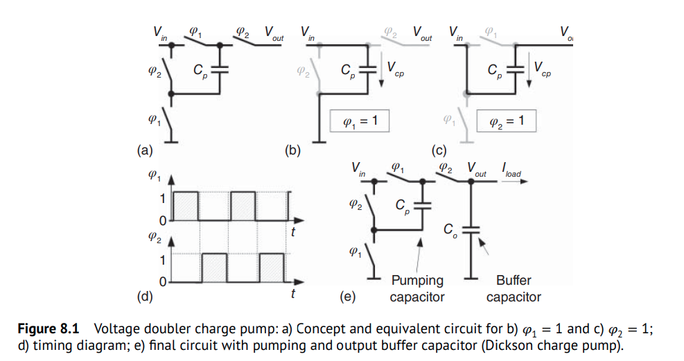
We derive a recursive equation that describes the output voltage
\(V_{out,n}\) after the \(n\)th clock cycle \[
V_{out,n} = \frac{2V_{in}C_p + V_{out,n-1}C_o}{C_p + C_o}
\]
Therefore, average output voltage \(\overline{V}_{out}\) in steady-state is
\[
\overline{V}_{out} = \frac{V_t+V_b}{2}=2V_{in} -
\frac{I_{load}}{f_{sw}C_p}\left(1 + \frac{C_p^2}{4C_o(C_p+C_o)}\right)
\approx 2V_{in} - \frac{I_{load}}{f_{sw}C_p}
\] which results in a simple expression for the output
voltage droop
\[
\Delta V_{out} = \frac{I_{load}}{f_{sw}C_p}
\]
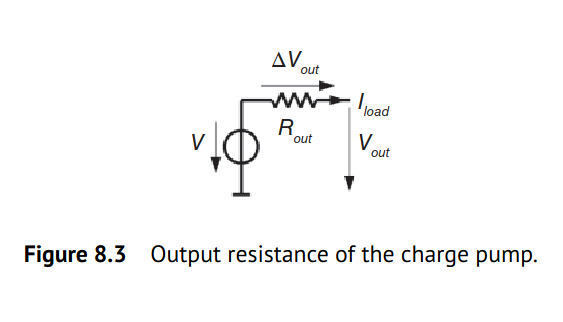
The charge pump can be modeled as a voltage source with a
source resistance\(R_\text{out}\). Therefore, \(\Delta V_{out}\) can be seen as the voltage
drop across \(R_\text{out}\) due to the
load current:
Hoi Lee, ISSCC2018 T8: Fundamentals of Switched-Mode Power Converter
Design [slides,transcript]
G. Palumbo and D. Pappalardo, "Charge Pump Circuits: An Overview on
Design Strategies and Topologies," in IEEE Circuits and Systems
Magazine, vol. 10, no. 1, pp. 31-45, First Quarter 2010 [pdf]
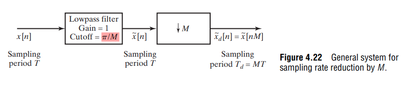
Fourier transform of the output of the expander is a frequency-scaled
version of the Fourier transform of the input
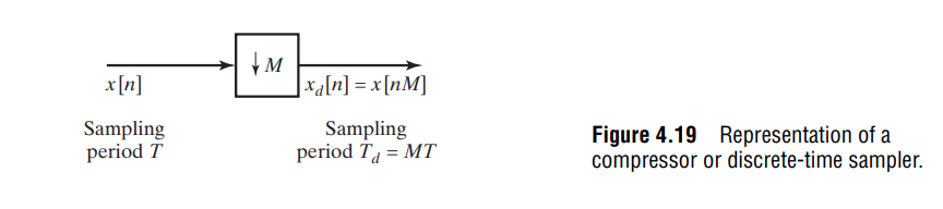
Subsampling or Downsampling
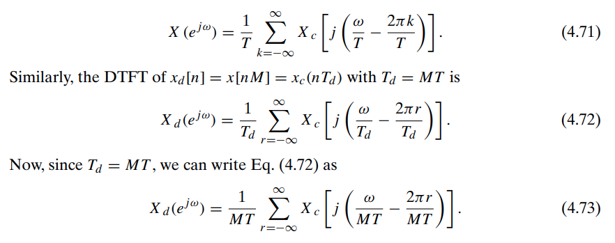
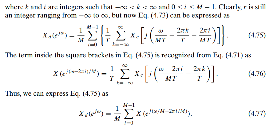
Eqs. (4.72)
the superposition of an infinite set of amplitude-scaled copies of
\(X_c(j\Omega)\), frequency scaled
through \(\omega = \Omega T_d\) and
shifted by integer multiples of \(2\pi\)
Eq. (4.77)
the superposition of \(M\)
amplitude-scaled copies of the periodic Fourier transform \(X (e^{j\omega})\), frequency scaled by
\(M\) and shifted by integer multiples
of \(2\pi\)
downsampled by a factor of \(M =
2\)
Upsampling or Zero Insertion
Rouphael, Tony. (2009). RF and Digital Signal Processing for
Software-Defined Radio. [pdf]
Assuming \(X(e^{j\omega_1}) =
U_f(e^{j\omega_1})\) with \(\omega_1 =
\Omega T_1\), upsampled by ratio \(L\), then obtain
Polyphase decomposition is a powerful technique used in digital
signal processing to efficiently implement multirate systems.
where \(e_k[n]=h[nM+k]\)
Polyphase Implementation of Decimation Filters &
Interpolation Filters
Decimation system
Interpolation system
sampling identity
LPTV Implementation
TODO 📅
The interpolation filter following an up-sampler
generally is time varying and cannot be represented by
a simple transfer function. The equivalent filter in a
zero-order hold is an exception, perhaps unique, that
can be represented with a time-invariant transfer function
The interpolation filter following an up-sampler generally is
time varying and cannot be represented by a simple
transfer function. The equivalent filter in a Zero-Order
Hold is an exception, perhaps unique, that can be represented
with a time-invariant transfer function
Split the \(1:LM\) hold process into
a \(1 : L\) hold followed by a \(1 : M\) hold \[
Y(\eta)=X(\eta^{L})\frac{1-\eta^{-L}}{1-\eta^{-1}}
\] then \[\begin{align}
F_2(z) &= Y(z^M)\cdot\frac{1-z^{-M}}{1-z^{-1}} \\
&=X(z^{LM})\frac{1-z^{-LM}}{1-z^{-M}}\cdot \frac{1-z^{-M}}{1-z^{-1}}
\\
&= X(z^{LM})\frac{1-z^{-LM}}{1-z^{-1}}
\end{align}\]
That is \(F_1(z)=F_2(z)\), i.e. they
are equivalent
In (a), the loop gain is \(\frac{\phi_o(z)}{\phi_e(z)}\), which is
\[
LG_a(z)=\frac{\phi_o(z)}{\phi_e(z)} = \frac{1}{1-z^{-1}}
\]
In (b),
Accumulate-And-Dump
(AAD) is \(\frac{1-z^{-L}}{1-z^{-1}}\), then \(\phi_m(\eta)\) can be expressed as \[
\phi_m(\eta) = \frac{1-\eta^{-1}}{1-\eta^{-1/L}}\cdot \frac{1}{L}
\] Hence \[\begin{align}
\phi_o(\eta) &= \phi_m(\eta) \frac{1}{1-\eta^{-1}} \\
&= \frac{1-\eta^{-1}}{1-\eta^{-1/L}}\cdot \frac{1}{L}\cdot
\frac{1}{1-\eta^{-1}}
\end{align}\]
After zero-order hold process, we obtain \(\phi_f(z)\), which is \[\begin{align}
\phi_f(z) &= \phi_o(z^L) \cdot \frac{1-z^{-L}}{1-z^{-1}} \\
&=\frac{1-z^{-L}}{1-z^{-1}}\cdot \frac{1}{L}\cdot
\frac{1}{1-z^{-L}}\cdot \frac{1-z^{-L}}{1-z^{-1}}
\end{align}\] i.e., \[
LG_b(z) = \frac{1}{1-z^{-1}}\cdot \frac{1}{L}\cdot
\frac{1-z^{-L}}{1-z^{-1}}
\]
When bandwidth is much less than sampling rate (data rate), \(\frac{1}{L}\cdot \frac{1-z^{-L}}{1-z^{-1}} \approx
1\)
Y. Xia et al., "A 10-GHz Low-Power Serial Digital Majority
Voter Based on Moving Accumulative Sign Filter in a PS-/PI-Based CDR,"
in IEEE Transactions on Microwave Theory and Techniques, vol.
68, no. 12 [https://sci-hub.se/10.1109/TMTT.2020.3029188]
J. Liang, A. Sheikholeslami. ISSCC2017. "A 28Gbps Digital CDR with
Adaptive Loop Gain for Optimum Jitter Tolerance" [slides,paper]
J. Liang, A. Sheikholeslami,, "Loop Gain Adaptation for Optimum
Jitter Tolerance in Digital CDRs," in IEEE Journal of Solid-State
Circuits [https://sci-hub.se/10.1109/JSSC.2018.2839038]
J. L. Sonntag and J. Stonick, "A Digital Clock and Data Recovery
Architecture for Multi-Gigabit/s Binary Links," in IEEE Journal of
Solid-State Circuits, vol. 41, no. 8, pp. 1867-1875, Aug. 2006 [https://sci-hub.se/10.1109/JSSC.2006.875292]
—, "A digital clock and data recovery architecture for
multi-gigabit/s binary links," Proceedings of the IEEE 2005 Custom
Integrated Circuits Conference, 2005.. [https://sci-hub.se/10.1109/CICC.2005.1568725]
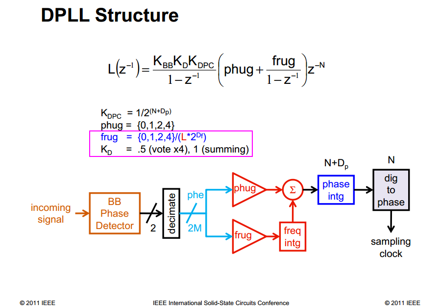
J. Stonick. ISSCC 2011 tutorials, T5: "DPLL-Based Clock and Data
Recovery"
Rhee, W. (2020). Phase-locked frequency generation and clocking :
architectures and circuits for modern wireless and wireline
systems. The Institution of Engineering and Technology
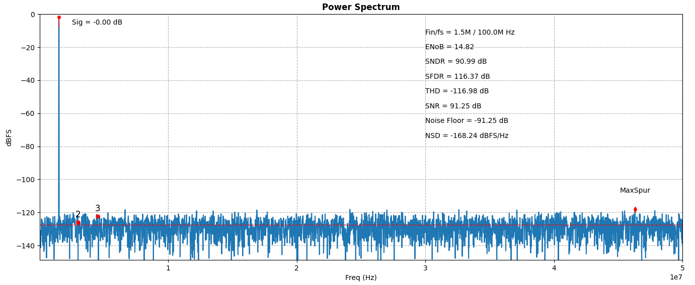
W. Liu, P. Huang and Y. Chiu, "A 12b 22.5/45MS/s 3.0mW 0.059mm2 CMOS
SAR ADC achieving over 90dB SFDR," 2010 IEEE International
Solid-State Circuits Conference - (ISSCC), San Francisco, CA, USA,
2010 [https://sci-hub.se/10.1109/ISSCC.2010.5433830]
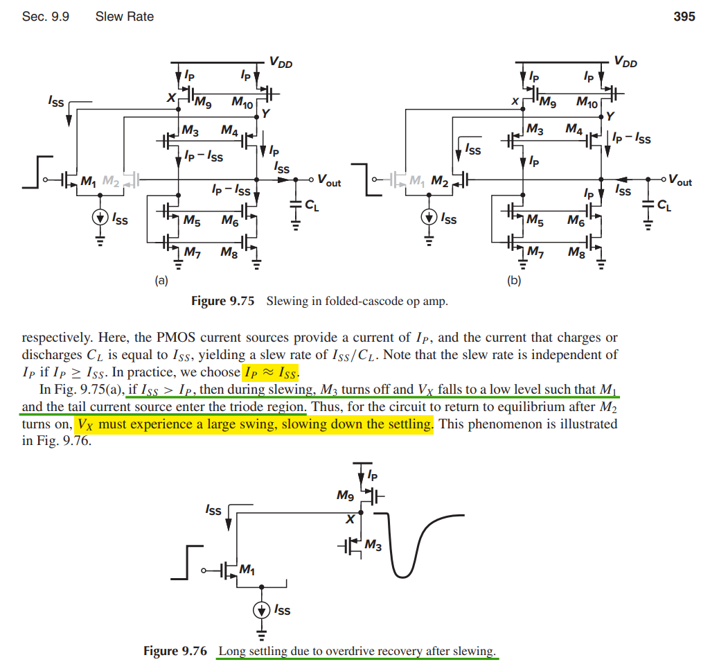
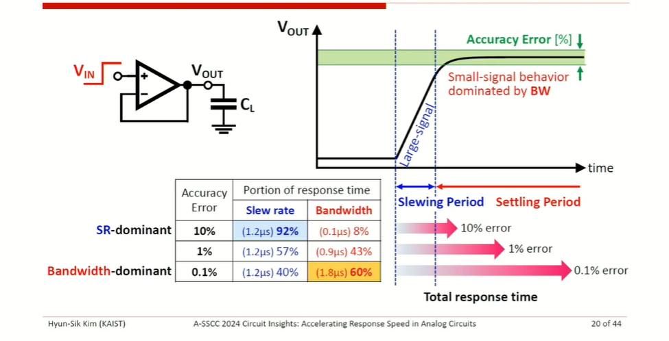
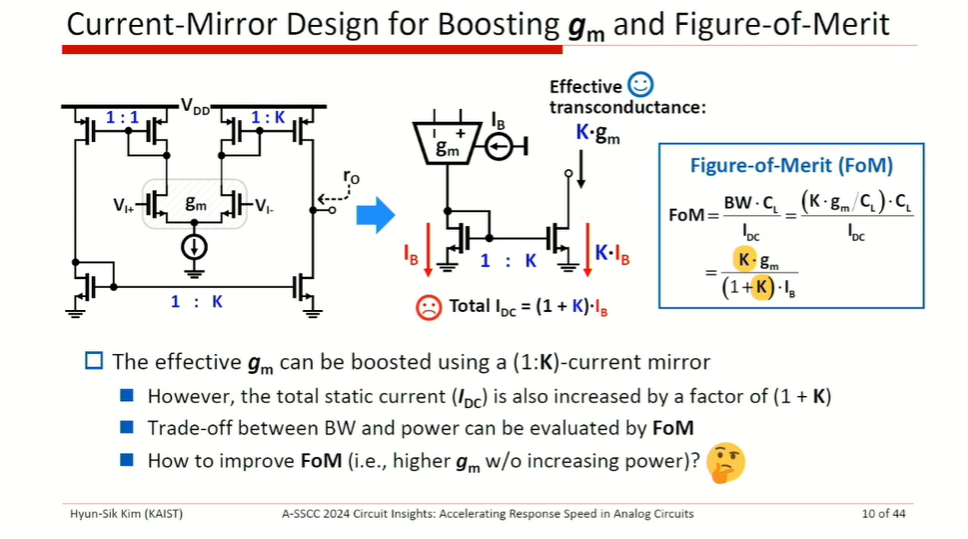
Slewing in Folded-Cascode Op
Amps
In practice, we choose \(I_P \simeq
I_{SS}\)
Avoid zero current in cascodes
left circuit
\(I_b \gt I_a\)
right circuit
\(I_b \gt 2I_a\)
Huijsing, J. H. (2017). Operational Amplifiers: Theory and Design. (3
ed.) Springer
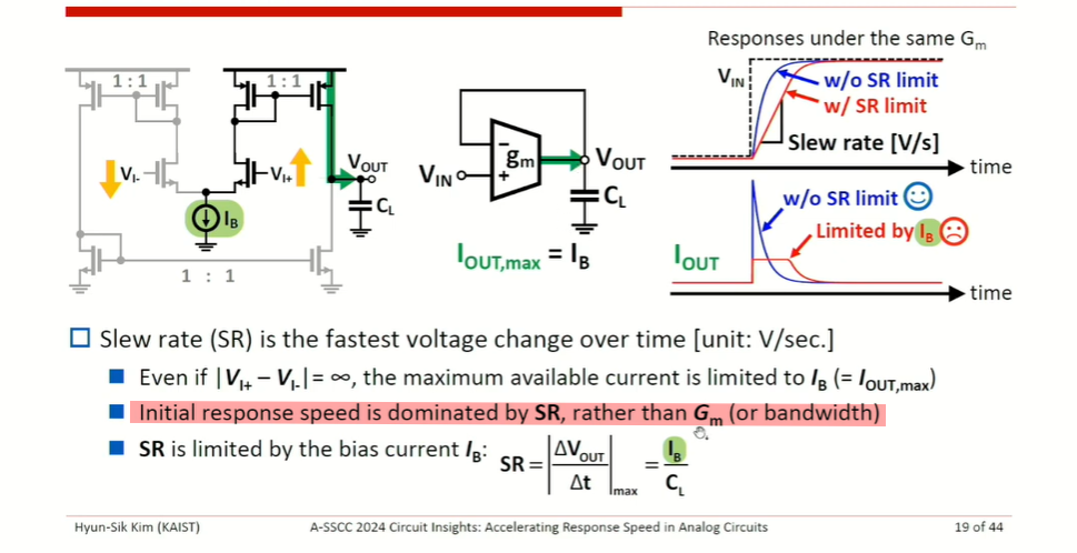
where \(\frac{g_m}{I_B} e^{-\omega_T t} \gt
1\) at initial response
Therefore, initial response speed is dominated by
SR, rather than \(G_m\) (or bandwidth)
MOS parasitic Rd&Rs, Cd&Cs
Decrease the parasitic R&C
priority: \(R_s \gt R_d\), \(C_s \gt C_d\)
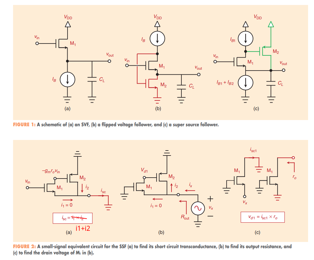
source follower
A. Sheikholeslami, "Voltage Follower, Part III [Circuit Intuitions],"
in IEEE Solid-State Circuits Magazine, vol. 15, no. 2, pp.
14-26, Spring 2023, doi: 10.1109/MSSC.2023.3269457
Z. Guo et al., "A 112.5Gb/s ADC-DSP-Based PAM-4 Long-Reach
Transceiver with >50dB Channel Loss in 5nm FinFET," 2022 IEEE
International Solid-State Circuits Conference (ISSCC), San Francisco,
CA, USA, 2022, pp. 116-118, doi: 10.1109/ISSCC42614.2022.9731650.
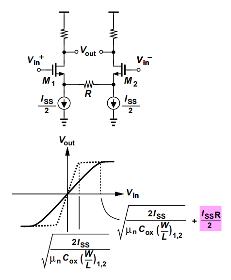
Resistive degeneration in differential pairs serves as one
major technique for linear amplifier
The linear region for CMOS differential pair would be extended by
\(±I_{SS}R/2\) as all of \(I_{SS}/2\) flows through \(R\). \[
V_{in}^+ -V_{in}^- = V_{OV} + V_{TH}+\frac{I_{SS}}{2}R - V_{TH} =
\sqrt{\frac{2I_{SS}}{\mu_nC_{OX}\frac{W}{L}}} + \frac{I_{SS}R}{2}
\]
Biasing
Tradeoffs in Resistive-Degenerated Diff Pair
w/ Current–Mirror Load
S. Pavan, "Revisiting the CMOS Differential Pair With a
Current–Mirror Load [CAS Education]," in IEEE Circuits and Systems
Magazine, vol. 25, no. 2, pp. 74-78, Secondquarter 2025 [pdf]
TODO 📅
Double Differential pair
\(V_\text{ip}\) and \(V_\text{im}\) are input, \(V_\text{rp}\) and \(V_\text{rm}\) are reference voltage \[
V_o = A_v(\overline{V_\text{ip} - V_\text{im}} - \overline{V_\text{rp} -
V_\text{rm}})
\]
In differential comparison mode, the feedback loop ensure \(V_\text{ip} = V_\text{rp}\), \(V_\text{im} = V_\text{rm}\) in the end
assume input and reference common voltage are
same
Pros of (b)
larger input range i.e., \(\gt \pm
\sqrt{2}V_\text{ov}\) of (a), it works even one
differential is off due to lower voltage
larger \(g_m\) (smaller input
difference of pair)
Cons of (b)
sensitive to the difference of common voltage between \(V_\text{ip}\), \(V_\text{im}\) and \(V_\text{rp}\), \(V_\text{rm}\)
common-mode voltage
difference
copy aforementioned formula here for convenience \[
V_o = A_v(\overline{V_\text{ip} - V_\text{im}} - \overline{V_\text{rp} -
V_\text{rm}})
\]
at sample phase\(V_\text{ip}=
V_\text{im}= V_\text{cmi}\) and \(V_\text{rp}= V_\text{rm}=
V_\text{cmr}\)
\(I_\text{ip0}= I_\text{im0} =
I_\text{i0}\)
\(I_\text{rp0}= I_\text{rm0} =
I_\text{r0}\)
i.e. \(\overline{I_\text{ip} + I_\text{rm}}
- \overline{I_\text{im} + I_\text{rp}} = 0\)
at compare start
\(V_\text{ip}= V_\text{im}=
V_\text{cmi}\) and \(V_\text{rp}=
V_\text{cmr}+\Delta\), \(V_\text{rp}=
V_\text{cmr}-\Delta\)
i.e. \(\overline{I_\text{ip} + I_\text{rm}}
- \overline{I_\text{im} + I_\text{rp}} \lt 0\), we need to
increase \(V_\text{ip}\) and decrease
\(V_\text{im}\).
and \(I_\text{ip0}= I_\text{im0} =
I_\text{i0}\), \(I_\text{rp0}=
I_\text{rm0} = I_\text{r0}\)
i.e. \(\overline{I_\text{ip} + I_\text{rm}}
- \overline{I_\text{im} + I_\text{rp}} = 0\)
If \(V_\text{cmr} - V_\text{cmi} =
\sqrt{2}V_{OV} + \delta\), and \(\delta
\gt 0\). one transistor carries the entire tail current
\(I_\text{ip} =0\) and \(I_\text{rp} = I_{SS}\), all the time
At the end, \(V_\text{im} = V_\text{cmi} -
(\Delta - \delta)\), the error is \(\delta\)
In closing, \(V_\text{cmr} - V_\text{cmi}
\lt \sqrt{2}V_{OV}\) for normal work
Furthermore, the difference between \(V_\text{cmr}\) and \(V_\text{cmi}\) should be minimized due to
limited impedance of current source and input
pair offset
In the end \[
V_\text{cmr} - V_\text{cmi} \lt \sqrt{2}V_{OV} - V_{OS}
\]
Under the condition, every transistor of pairs are on in
equilibrium
We obtain \[
\sigma_{vos,DE} = 2\sigma_{vos,SE}
\]
Gm/ID Approach in Transistor
Sizing
Hesham Omran, The Analog Designer's Toolbox (ADT) | Invited Talk by
IEEE Santa Clara Valley Section CAS Society [https://youtu.be/FT6kKC5OdE0]
Jespers, P. G. A., & Murmann, B. (2017). Systematic Design of
Analog CMOS Circuits: Using Pre-Computed Lookup Tables. Cambridge:
Cambridge University Press.
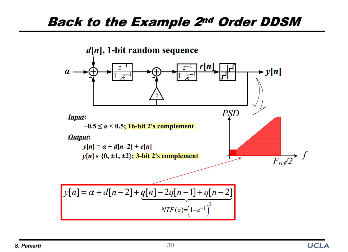
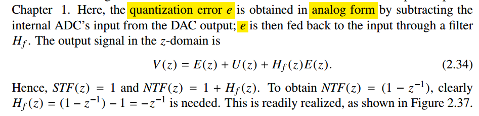
In \(z\)-domain \[
\left\{(A + D - Y)\frac{z^{-1}}{1-z^{-1}} - 2Y
\right\}\frac{z^{-1}}{1-z^{-1}} + Q = Y
\] That is \[
Y = A z^{-2} + Dz^{-2} + Q(1-z^{-1})^2
\] In time domain \[\begin{align}
y[n] &= \alpha[n-2] + d[n-2] + q[n]-2q[n-1]+q[n-2] \\
&= \alpha + d[n-2] + q[n]-2q[n-1]+q[n-2]
\end{align}\]
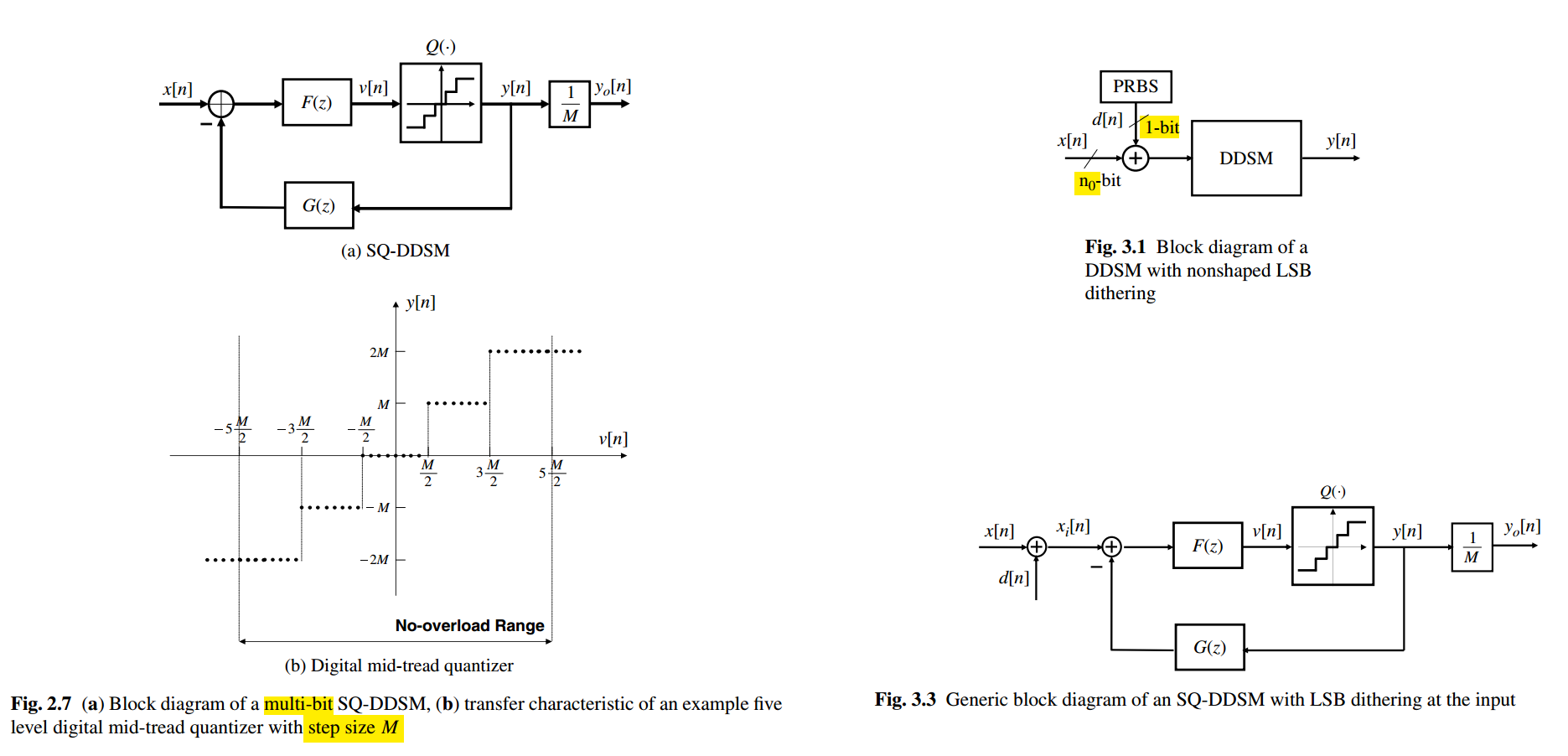
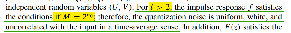
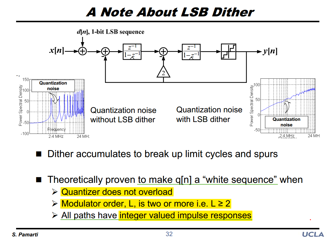
LSB Dither
?? integer valued impulse responses
S. Pamarti, J. Welz and I. Galton, "Statistics of the Quantization
Noise in 1-Bit Dithered Single-Quantizer Digital Delta–Sigma
Modulators," in IEEE Transactions on Circuits and Systems I: Regular
Papers, vol. 54, no. 3, pp. 492-503, March 2007 [pdf]
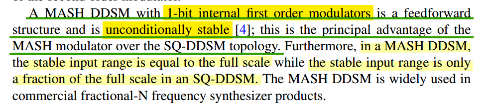
stability of DSM
accumulator wordlength
Z. Ye and M. P. Kennedy, "Hardware Reduction in Digital Delta–Sigma
Modulators Via Error Masking—Part II: SQ-DDSM," in IEEE Transactions
on Circuits and Systems II: Express Briefs, vol. 56, no. 2, pp.
112-116, Feb. 2009 [https://sci-hub.se/10.1109/TCSII.2008.2010188]
—, "Hardware Reduction in Digital Delta-Sigma Modulators Via Error
Masking - Part I: MASH DDSM," in IEEE Transactions on Circuits and
Systems I: Regular Papers, vol. 56, no. 4, pp. 714-726, April 2009
[https://sci-hub.se/10.1109/TCSI.2008.2003383]
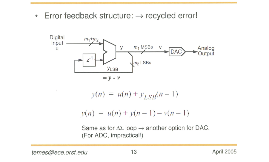
Truncation DAC
accumulator is implicit quantizer
with \(\frac{y}{2^{m_2}} + q= v\),
where \(v =
\lfloor\frac{y}{2^{m_2}}\rfloor\)
\[
\left\{ \begin{array}{cl}
Y + 2^{m_2} Q &= 2^{m_2}V \\
U - z^{-1}2^{m_2}Q &= Y
\end{array} \right.
\]
The STF & NTF is shown as below \[
V = \frac{1}{2^{m_2}}U + (1-z^{-1})Q
\]
To avoid accumulator overflow, stable input range is only
of a fraction of the full scale ( \(2^{m_1+m_2}-1\)) \[
u \leq 2^{m_1+m_2} - 2^{m_2}
\]
—. "LSB Dithering in MASH Delta–Sigma D/A Converters," in IEEE
Transactions on Circuits and Systems I: Regular Papers, vol. 54,
no. 4, pp. 779-790, April 2007 [https://sci-hub.se/10.1109/TCSI.2006.888780]
—. CICC 2020 ES2-2: Basics of Closed- and Open-Loop Fractional
Frequency Synthesis [https://youtu.be/t1TY-D95CY8]
i.e. \[
\tau[n] = \tau[n-1] + (y[n] - \alpha)T_{PLL}
\]
where \(\tau[n] = t_{v_{DIV}} - t_{v_{DIV},
desired}\)
Y. Zhang et al., "A Fractional- N PLL With Space–Time
Averaging for Quantization Noise Reduction," in IEEE Journal of
Solid-State Circuits, vol. 55, no. 3, pp. 602-614, March 2020, [pdf]
X. Wang and M. P. Kennedy, "Unified Analysis of Digital Δ-Σ
Modulators (DDSMs) for Fractional-N Frequency Synthesis—Introducing the
PASS Family of DDSMs Featuring Independent Shaping of the Probability
Density and Spectral Envelope," in IEEE Transactions on Circuits and
Systems I: Regular Papers [link]
X. Wang and M. P. Kennedy, "Performance Limits of Fractional-N
Digital PLLs with Mid-Rise TDCs," 2023 18th Conference on Ph.D Research
in Microelectronics and Electronics (PRIME), Valencia, Spain, 2023 [link]
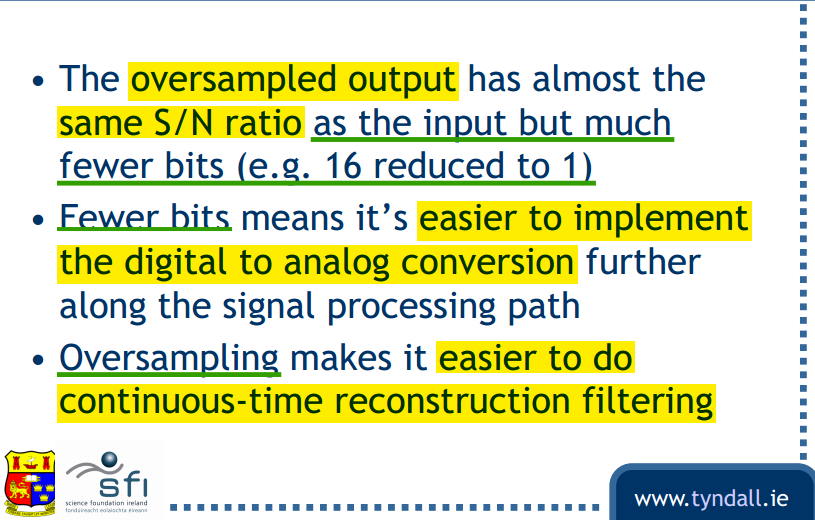
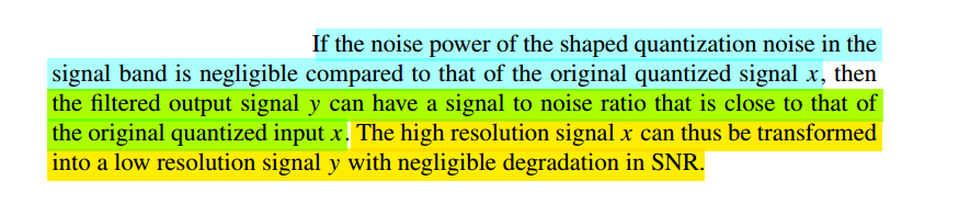
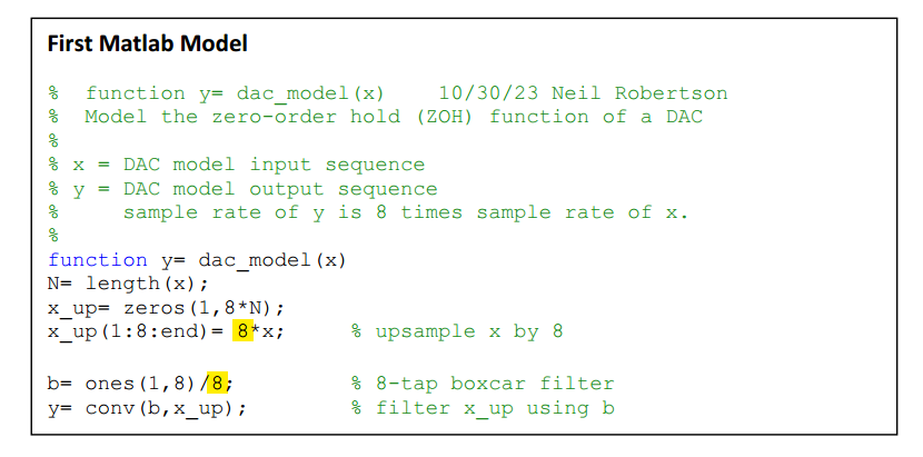
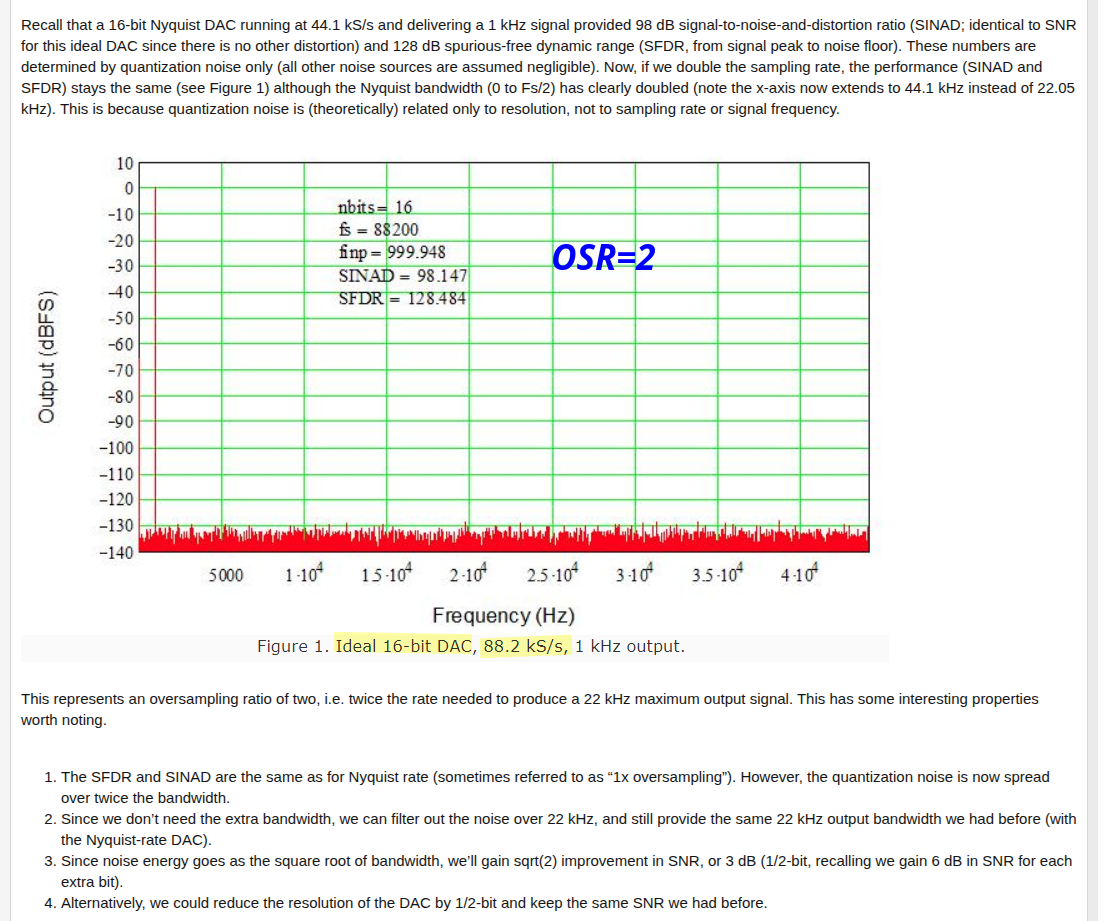
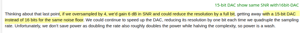
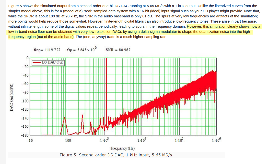
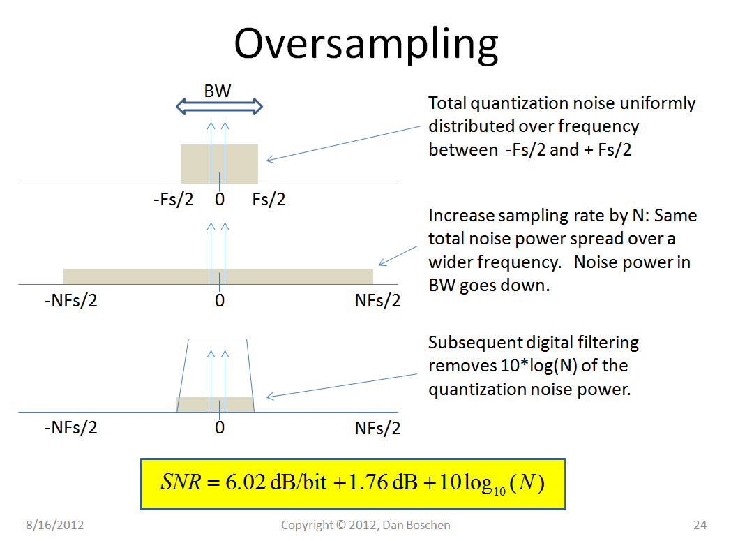
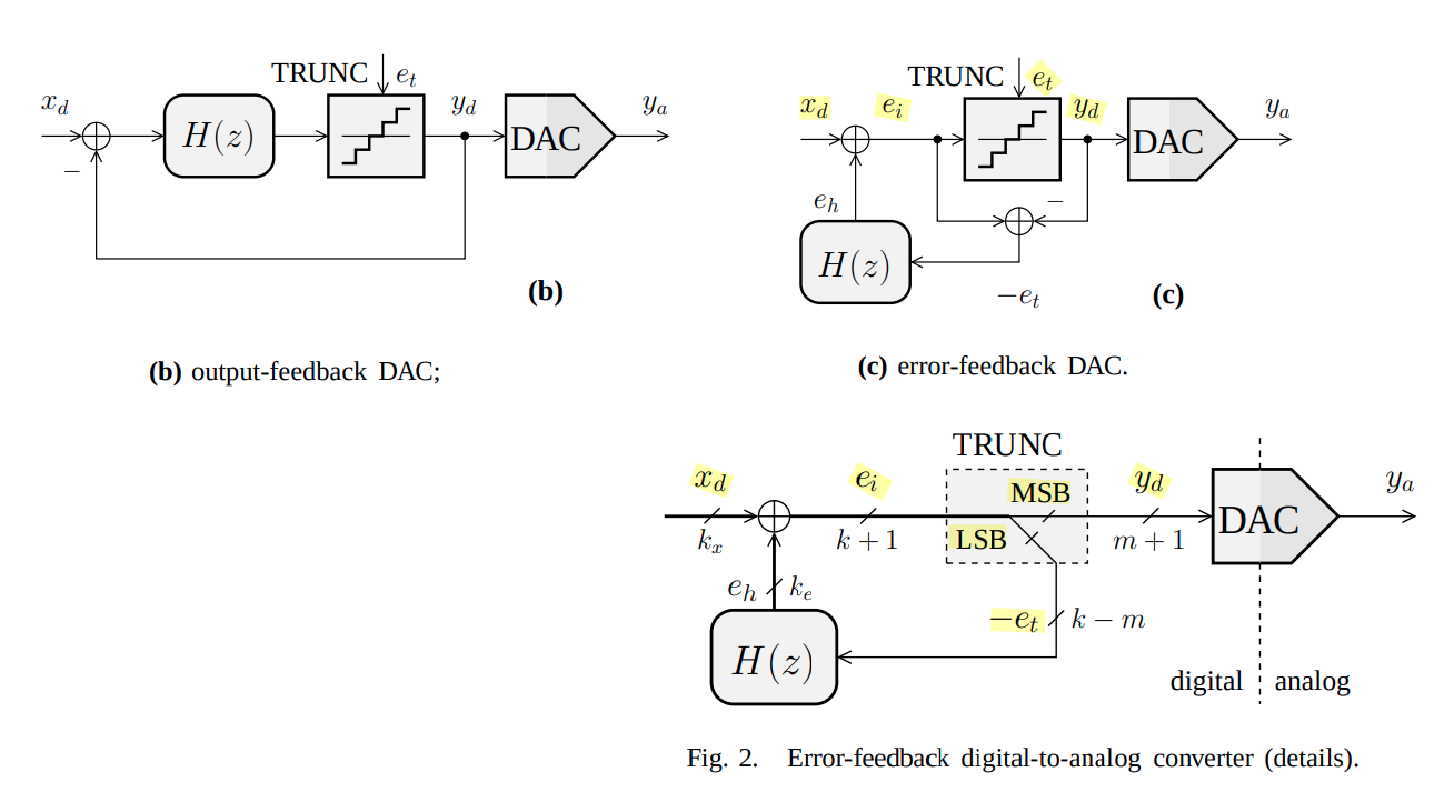
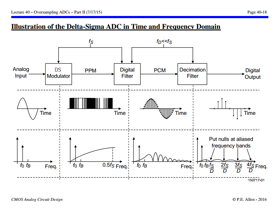
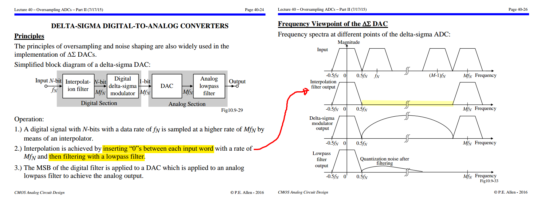
Sigma-delta digital-to-analog converters (SD DAC’s) are often used
for discrete-time signals with sample rate much higher than
their bandwidth
Because of the high sample rate relative to signal bandwidth,
a very simple DAC reconstruction filter (Analog
lowpass filter) suffices, often just a one-pole RC
lowpass
1 2 3 4 5 6 7 8 9 10 11 12 13 14 15
R= 4.7e3; % ohms resistor value C= .01e-6; % F capacitor value fs= 1e6; % Hz DAC sample rate % input signal x= [zeros(1,20) .9*ones(1,200) .1*ones(1,200)]; % find output y of SD DAC and output y_filt of RC filter [y,y_filt]= sd_dacRC(x,R,C,fs);
t = linspace(0,length(x)-1, length(x))*1/fs*1e3; subplot(3,1,1) plot(t, x, '.'); title('x'); grid on subplot(3,1,2) plot(t, y, '.'); title('y'); grid on subplot(3,1,3) plot(t, y_filt); title('y_{filt}'); xlabel('t(ms)'); grid on
% https://www.dsprelated.com/showarticle/1642.php % Neil Robertson, Model a Sigma-Delta DAC Plus RC Filter
% function [y,y_filt] = sd_dacRC(x,R,C,fs) 2/5/24 Neil Robertson % 1-bit sigma-delta DAC with RC filter % Model does not include a zero-order hold. % % x = input signal vector, 0 <= x < 1 % R = series resistor value, Ohms. Normally R > 1000 for 3.3 V logic. % C = shunt capacitor value, Farads % fs = sample frequency, Hz % y = DAC output signal vector, y(n) = 0 or 1 % y_filt = RC filter output signal vector % function[y,y_filt] = sd_dacRC(x,R,C,fs) N= length(x); x= fix(x*2^16)/2^16; % quantize x to 16 bits %I 1-bit Sigma-delta DAC s= [x(1) zeros(1,N-1)]; for n= 2:N u= x(n) + s(n-1); s(n)= mod(u,1); % sum y(n)= fix(u); % carry end
%II One-pole RC filter model % Matched z-Transform https://ocw.mit.edu/courses/2-161-signal-processing-continuous-and-discrete-fall-2008/cc00ac6d468dc9dcf2238fc1d1a194d4_lecture_19.pdf Ts= 1/fs; Wc= 1/(R*C); % rad -3 dB frequency fc= Wc/(2*pi); % Hz -3 dB frequency a1= -exp(-Wc*Ts); b0= 1 + a1; % numerator coefficient a= [1 a1]; % denominator coeffs y_filt= filter(b0,a,y); % filter the DAC's output signal y
J. W. M. Rogers, F. F. Dai, M. S. Cavin and D. G. Rahn, "A multiband
/spl Delta//spl Sigma/ fractional-N frequency synthesizer for a MIMO
WLAN transceiver RFIC," in IEEE Journal of Solid-State
Circuits, vol. 40, no. 3, pp. 678-689, March 2005 [https://sci-hub.se/10.1109/JSSC.2005.843604]
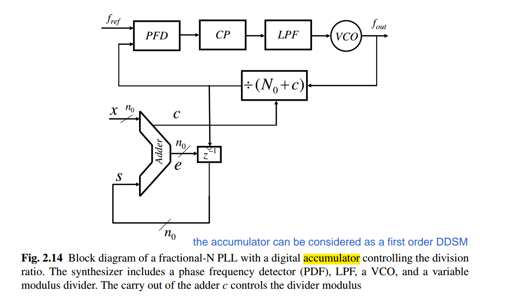
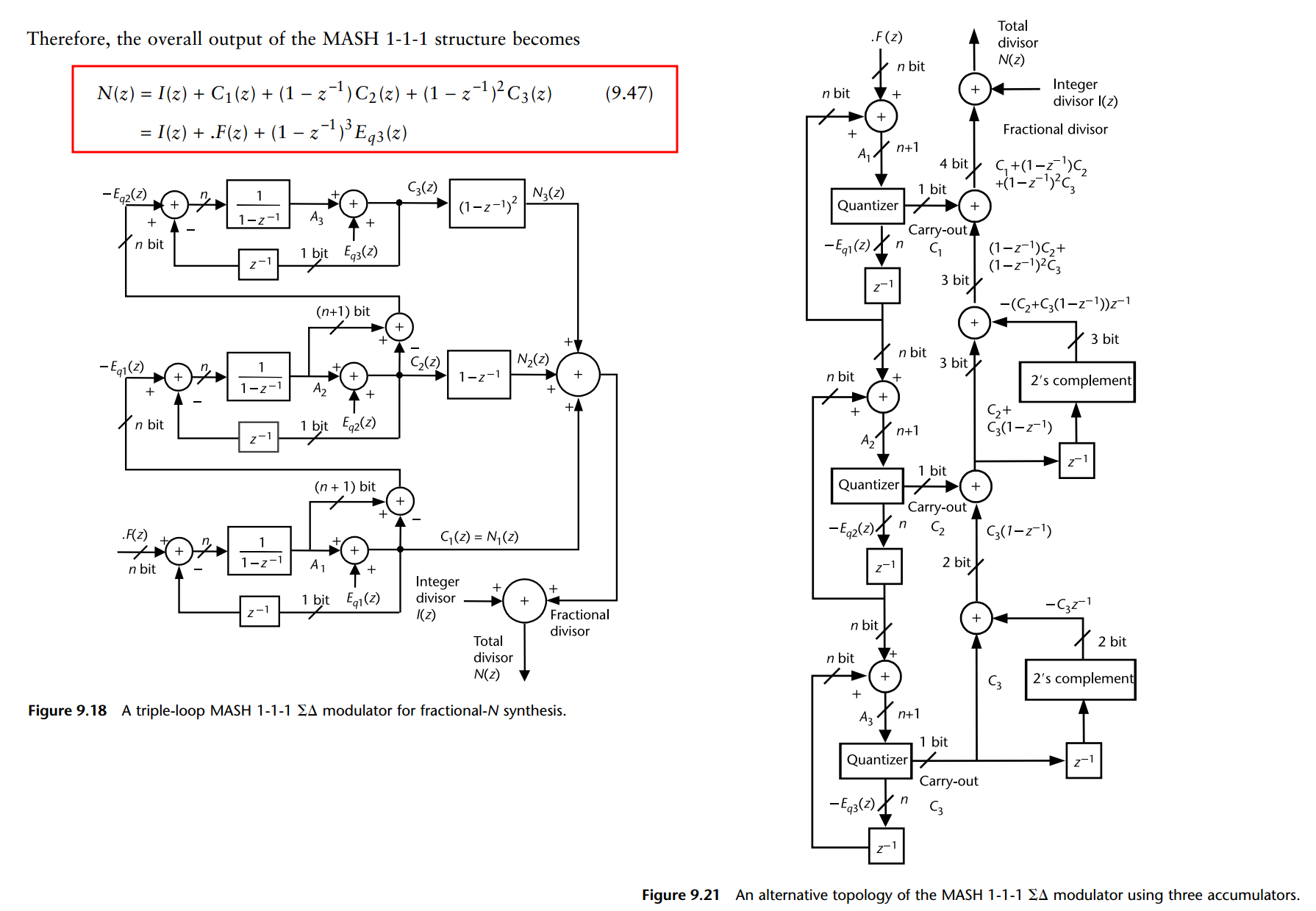
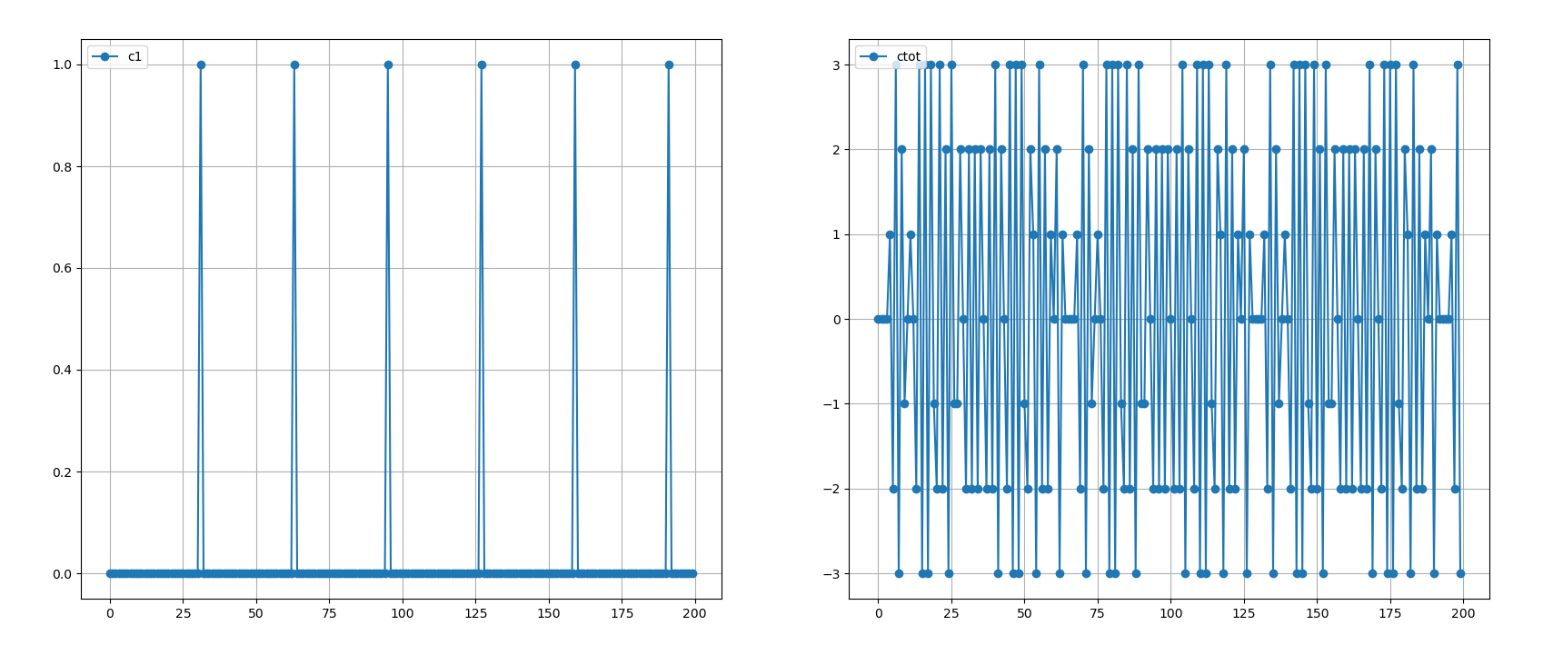
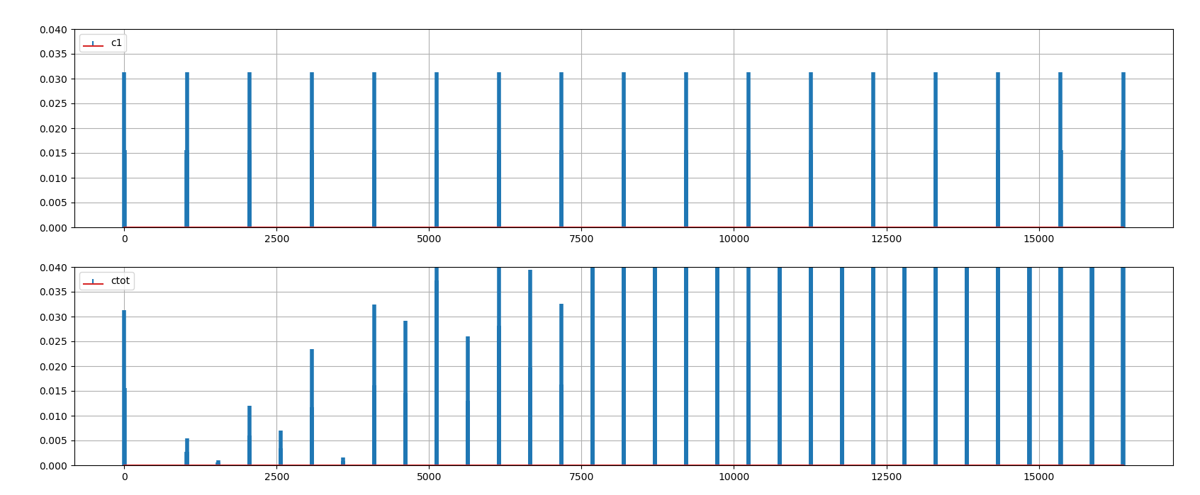
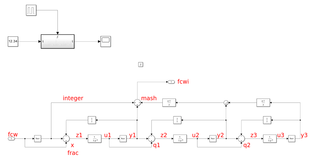
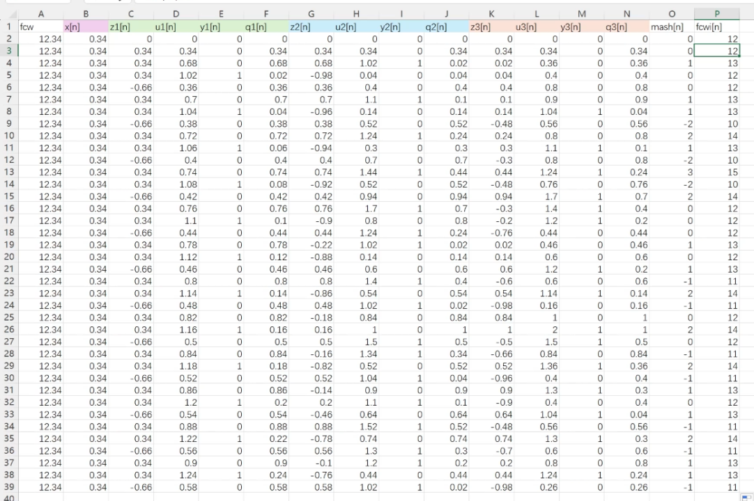
(a) a fractional accumulator, and (b) a triple-loop \(\Delta\Sigma\) accumulator for \(N(z) = 100 + 1/32\)
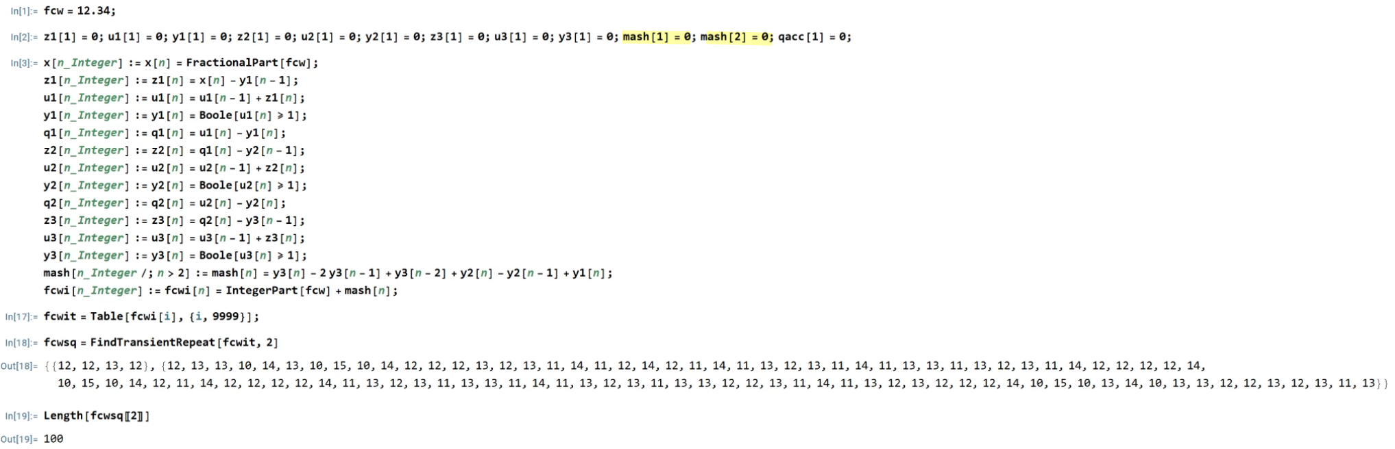
The code fcwit = Table[fcwi[i], {i, 9999}]; is the
command that actually runs the simulation for a set
duration.
Here is the breakdown of what is happening:
Table[..., {i, 9999}]: This creates a
list by repeating an operation 9,999 times. It acts like a
for loop in other programming languages.
fcwi[i]: This calls the function you
defined earlier. For every value of i from 1 to 9,999, it
calculates the instantaneous integer division ratio produced by the MASH
modulator.
fcwit = ...: It stores all 9,999
results into a single long list (an array) named
fcwit.
; (Semicolon): This is important—it
suppresses the output. Without it, Mathematica would print all 9,999
numbers on your screen, which would be a huge mess!
reference
Michael Peter Kennedy. scv-cas 2014: Digital Delta-Sigma Modulators
[pdf,recording]
—, Recent advances in the analysis, design and optimization of
Digital Delta-Sigma Modulators [pdf]
Kaveh Hosseini and Peter Kennedy. 2006 Hardware Efficient Maximum
Sequence Length Digital MASH Delta Sigma Modulator [pdf]
Pavan, Shanthi, Richard Schreier, and Gabor Temes. (2016) 2016.
Understanding Delta-Sigma Data Converters. 2nd ed. Wiley.
John Rogers, Calvin Plett, and Foster Dai. 2006. Integrated Circuit
Design for High-Speed Frequency Synthesis (Artech House Microwave
Library). Artech House, Inc., USA.
K. Hosseini and M. P. Kennedy, Minimizing Spurious Tones in Digital
Delta-Sigma Modulators (Analog Circuits and Signal Processing). New
York, NY, USA: Springer, 2011.
Rhee, W. (2020). Phase-locked frequency generation and clocking :
architectures and circuits for modern wireless and wireline
systems. The Institution of Engineering and Technology
Lacaita, Andrea Leonardo, Salvatore Levantino, and Carlo Samori.
Integrated frequency synthesizers for wireless systems.
Cambridge University Press, 2007.
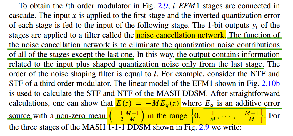
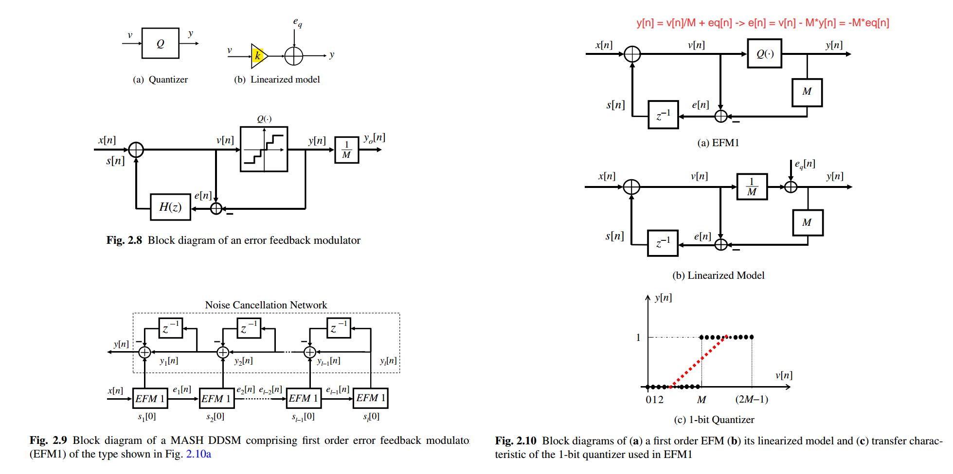
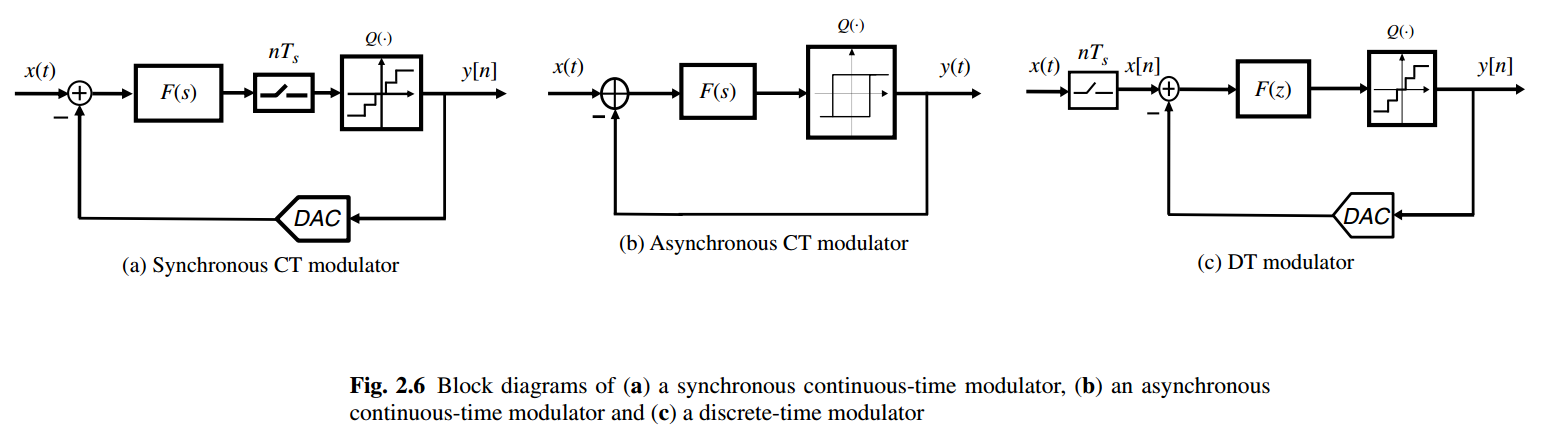
Delta-Sigma Modulators │ ├─ Analog ΔΣ Modulators │ │ │ ├─ Discrete-Time Analog ΔΣ Modulator, DT ΔΣM │ │ ├─ Switched-capacitor / switched-current loop filter │ │ ├─ Input is sampled before or inside loop filter │ │ └─ Very common in ΔΣ ADCs │ │ │ └─ Continuous-Time Analog ΔΣ Modulator, CT ΔΣM │ ├─ Continuous-time RC / gm-C / active-RC loop filter │ ├─ Feedback DAC is continuous-time │ ├─ Quantizer is usually clocked → synchronous CT ΔΣM │ └─ Quantizer/comparator may be event-driven → asynchronous CT ΔΣM │ └─ Digital ΔΣ Modulators, DDSM │ ├─ Single-quantizer DDSM │ ├─ Output-feedback form │ └─ Error-feedback form, EFM │ └─ MASH DDSM └─ Multi-stage noise-shaping modulator
"Quantizers" and "truncators",
"integrators" and "accumulators" are
used in delta-sigma ADCs and DACs,
respectively
P. Kiss, J. Arias and Dandan Li, "Stable high-order delta-sigma
DACS," 2003 IEEE International Symposium on Circuits and Systems
(ISCAS), Bangkok, 2003 [https://www.ele.uva.es/~jesus/analog/tcasi2003.pdf]
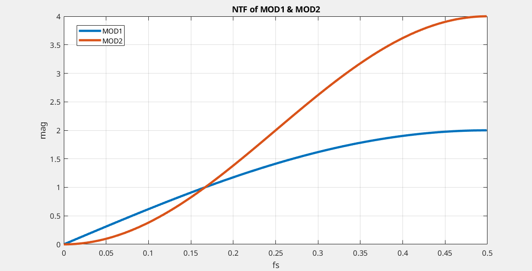
plot(w1/2/pi, abs(h1), LineWidth=3) hold on plot(w2/2/pi, abs(h2), LineWidth=3) grid on legend('MOD1', 'MOD2') xlabel('fs') ylabel('mag') title('NTF of MOD1 & MOD2')
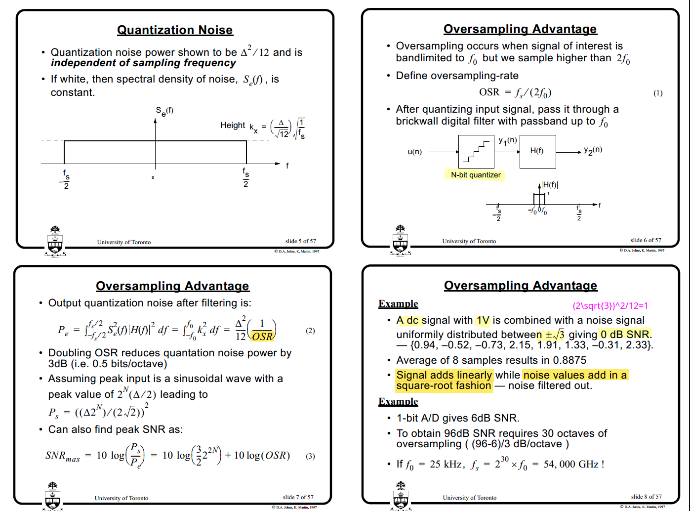
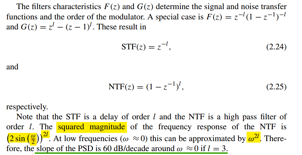
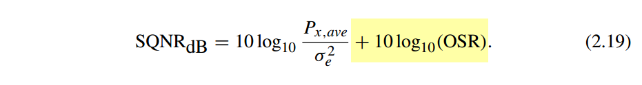
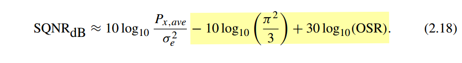
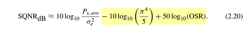
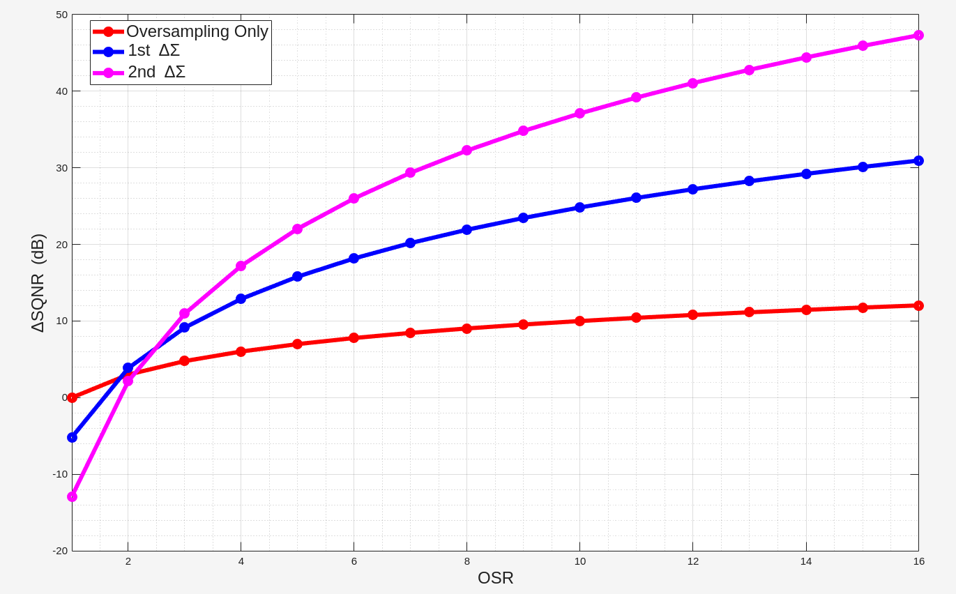
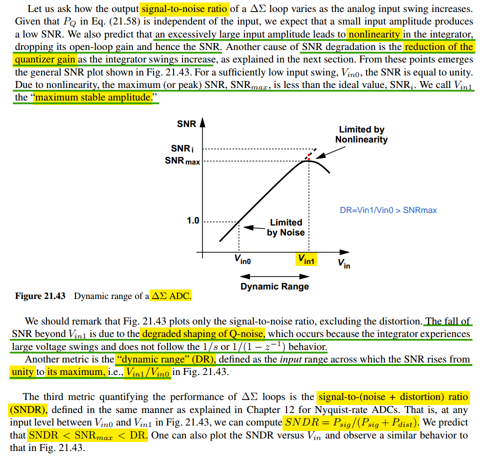
SQNR improvement
In general, for an \(l\)th order
modulator with \(\text{NTF}(z) = (1 −
z^{−1})^l\), the SQNR increases by \((6l + 3)\) dB for every
doubling of the OSR, which provides \(l+0.5\)extra bits
resolution
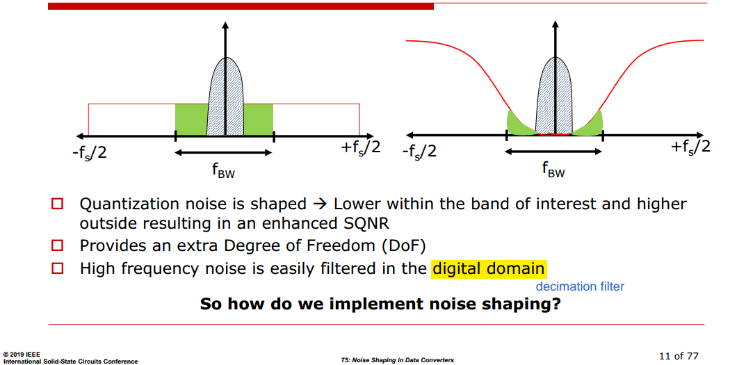
\(\Delta \Sigma\) modulators,
and other noise-shaping modulators, change the spectrum of the
noise but leave the signal unchanged
\(\Delta\) modulators and other
signal-predicting modulators shape the spectrum of the
modulated signal but leave the quantization noise unchanged at the
receiver
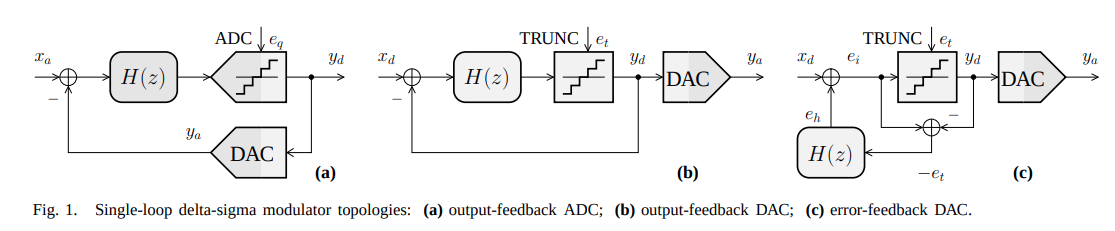
output vs.
error-feedback
The error-feedback architecture is
problematic for analog implementation, since it is
sensitive to variations of its parameters (subtractor
realization)
ADC
DAC
P. Kiss, J. Arias and Dandan Li, "Stable high-order delta-sigma
DACS," 2003 IEEE International Symposium on Circuits and Systems
(ISCAS), Bangkok, 2003 [https://www.ele.uva.es/~jesus/analog/tcasi2003.pdf]
always @(*) i_func_extended = {i_func[15],i_func[15],i_func[15],i_func[15],i_func}; always @(posedge i_clk ornegedge i_res) begin if (i_res==0) begin DAC_acc_1st<=16'd0; DAC_acc_2nd<=16'd0; this_bit = 1'b0; end elseif(i_ce == 1'b1) begin if(this_bit == 1'b1) begin DAC_acc_1st = DAC_acc_1st + i_func_extended - (2**15); DAC_acc_2nd = DAC_acc_2nd + DAC_acc_1st - (2**15); end else begin DAC_acc_1st = DAC_acc_1st + i_func_extended + (2**15); DAC_acc_2nd = DAC_acc_2nd + DAC_acc_1st + (2**15); end // When the high bit is set (a negative value) we need to output a 0 and when it is clear we need to output a 1. this_bit = ~DAC_acc_2nd[19]; end end endmodule
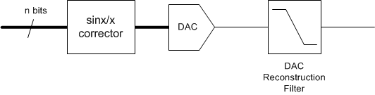
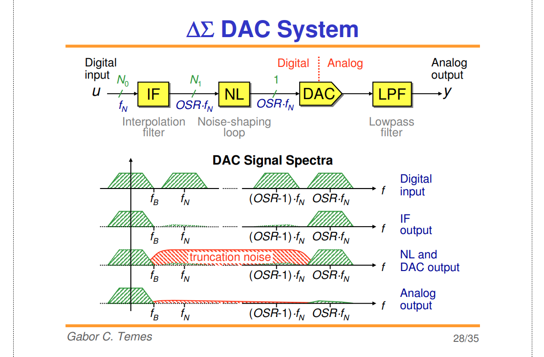
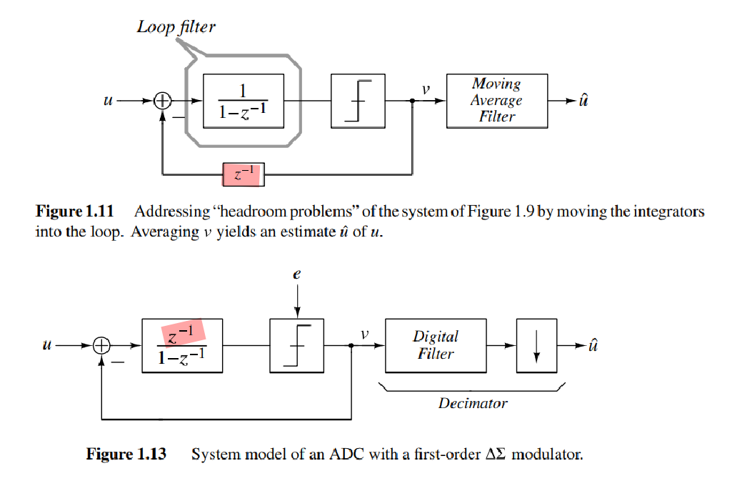
an interpolation filter effectively
up-samples its low-rate input and
lowpass-filters the resulting high-rate data
to produce a high-rate output devoid of images
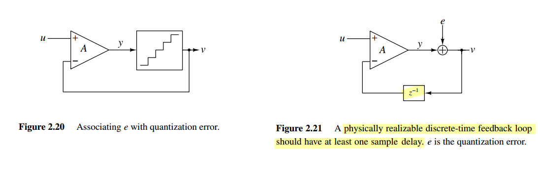
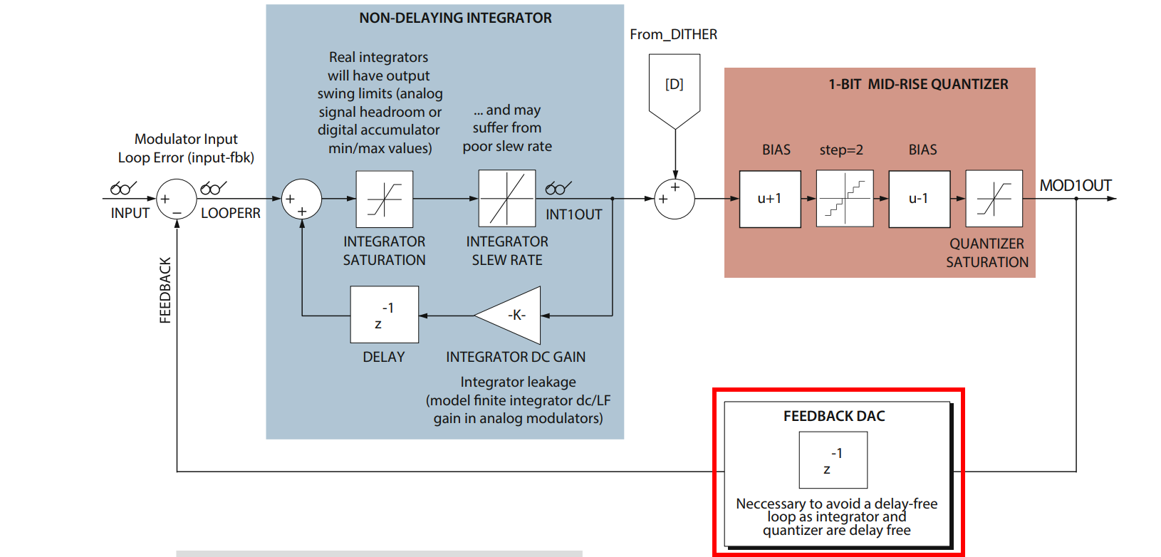
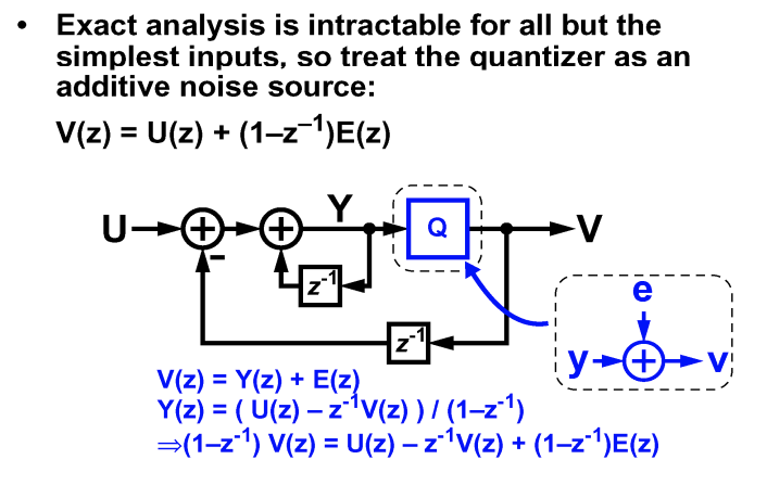
Any such physically feasible device will take
a finite time to operate – in other words, the
quantized output will only be available a small time
after the quantizer has "looked" at the input - insert a one-sample
delay
there cannot be a "delay free loop" is a
common idea in sequential digital state machine design
Both integrator and quantizer are delay free
NTF realizability criterion: No delay-free loops in the modulator
linear settling & GBW of
amplifier
TODO 📅
Switched capacitor has been the common realization technique of
discrete-time (DT) modulators, and in order to achieve a
linear settling, the sampling frequency used
in these converters needs to be significantly lower than the gain
bandwidth product (GBW) of the amplifiers.
function[v,xn,xmax,y] = simulateDSM(u,arg2,nlev,x0) %[v,xn,xmax,y] = simulateDSM(u,ABCD,nlev=2,x0=0) % or %[v,xn,xmax,y] = simulateDSM(u,ntf,nlev=2,x0=0) % %Compute the output of a general delta-sigma modulator with input u, %a structure described by ABCD, an initial state x0 (default zero) and %a quantizer with a number of levels specified by nlev. %Multiple quantizers are implied by making nlev an array, %and multiple inputs are implied by the number of rows in u. % %Alternatively, the modulator may be described by an NTF. %The NTF is zpk object. (The STF is assumed to be 1.) %The structure that is simulated is the block-diagional structure used by %zp2ss.m.
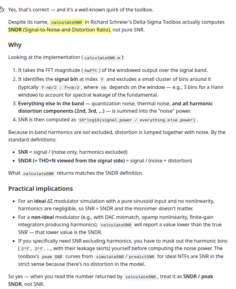
calculateSNR
1 2 3 4 5 6 7 8 9 10 11 12
functionsnr = calculateSNR(hwfft,f,nsig)
signalBins = [f-nsig+1:f+nsig+1]; s = norm(hwfft(signalBins));
noiseBins = 1:length(hwfft); noiseBins(signalBins) = []; n = norm(hwfft(noiseBins));
snr = dbv(s/n);
end
reference
Pavan, Shanthi, Richard Schreier, and Gabor Temes. (2016).
Understanding Delta-Sigma Data Converters. 2nd ed. Wiley.
Norsworthy, Steven R., Richard Schreier, Gábor C. Temes and Ieee
Circuits. “Delta-sigma data converters : theory, design, and
simulation.” (1997).
Horowitz, P., & Hill, W. (2015). The art of electronics
(3rd ed.). Cambridge University Press.
John Rogers, Calvin Plett, and Foster Dai. 2006. Integrated Circuit
Design for High-Speed Frequency Synthesis (Artech House Microwave
Library). Artech House, Inc., USA.
Razavi B. Analysis and Design of Data Converters. Cambridge
University Press; 2025.
R. Schreier, ISSCC2006 tutorial: Understanding Delta-Sigma Data
Converters
P. M. Aziz, H. V. Sorensen and J. vn der Spiegel, "An overview of
sigma-delta converters," in IEEE Signal Processing Magazine, vol. 13,
no. 1, pp. 61-84, Jan. 1996 [https://sci-hub.st/10.1109/79.482138]
V. Medina, P. Rombouts and L. Hernandez-Corporales, "A Different View
of Sigma-Delta Modulators Under the Lens of Pulse Frequency Modulation
[Feature]," in IEEE Circuits and Systems Magazine, vol. 24, no.
2, pp. 80-97, Secondquarter 2024
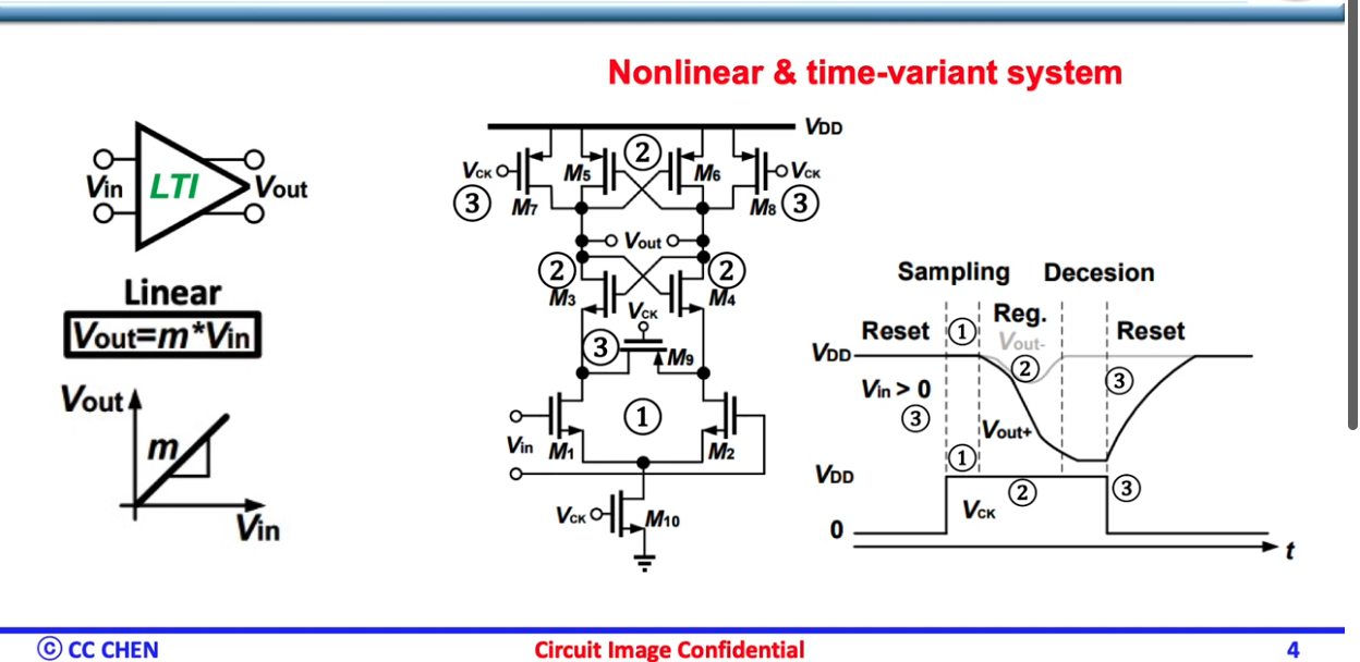
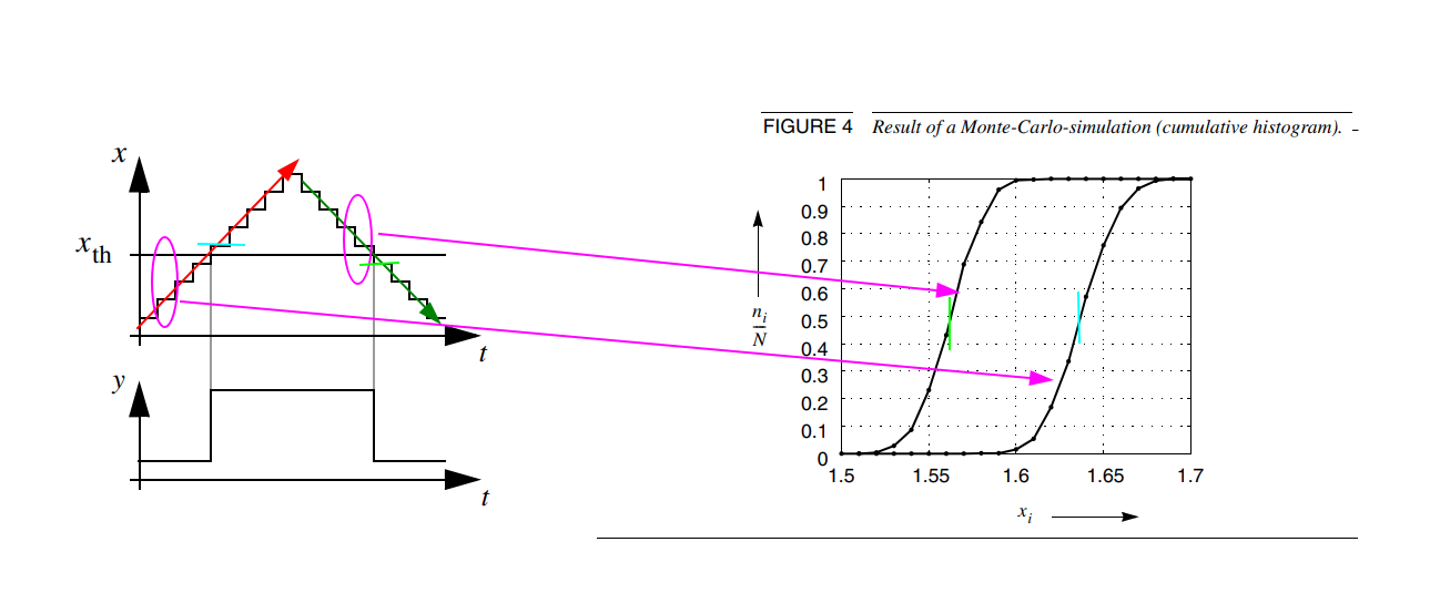
Comparator Output SNR during sampling region and decision region go
up
Comparator Output SNR during regeneration region is
constant, where noise is critical
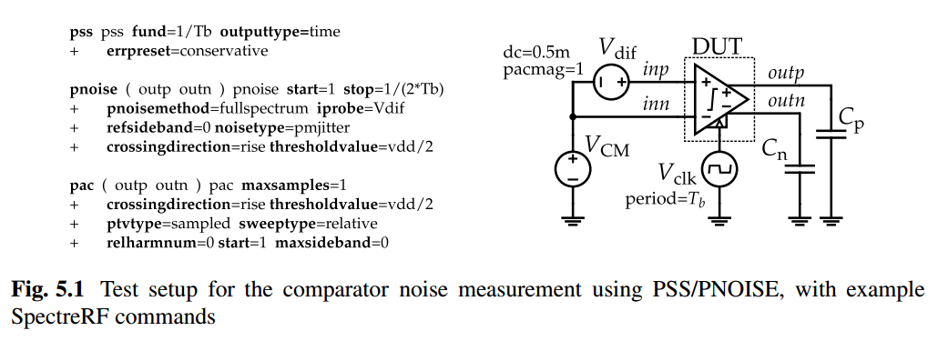
Transient Noise Method
Noise Fmax sets the bandwidth of the random noise
sources that are injected at each time point in the transient
analysis
We can identify the RMS noise value easily by looking at 15.9% or
84.1% of CDF (\(1\sigma\)), the
input-referred noise in the RMS is 0.9mV
Thus, if \(V_S\) is chosen so as to
reduce the probability of zeros to 16%, then \(V_S = 1\sigma\), which is also the total
root-mean square (rms) noise referred to the input.
Comparison of two methods
here, fundamental frequency = fclk; integrated noise (0 ~
0.5fclk)
E. Gillen, G. Panchanan, B. Lawton and D. O'Hare, "Comparison of
transient and PNOISE simulation techniques for the design of a dynamic
comparator," 2022 33rd Irish Signals and Systems Conference (ISSC),
Cork, Ireland, 2022, pp. 1-5
J. Conrad, J. Kauffman, S. Wilhelmstatter, R. Asthana, V. Belagiannis
and M. Ortmanns, "Confidence Estimation and Boosting for
Dynamic-Comparator Transient-Noise Analysis," 2024 22nd IEEE
Interregional NEWCAS Conference (NEWCAS), Sherbrooke, QC, Canada,
2024, pp. 1-5
There are some ambiguity in formula in ADC Verification Rapid
Adoption Kit (RAK)(Product Version: IC 6.1.8, SPECTRE 18.1 March,
2019)
Transient Noise Analysis: \(\sqrt{2}\sigma\), why ratio \(\sqrt{2}\) ???
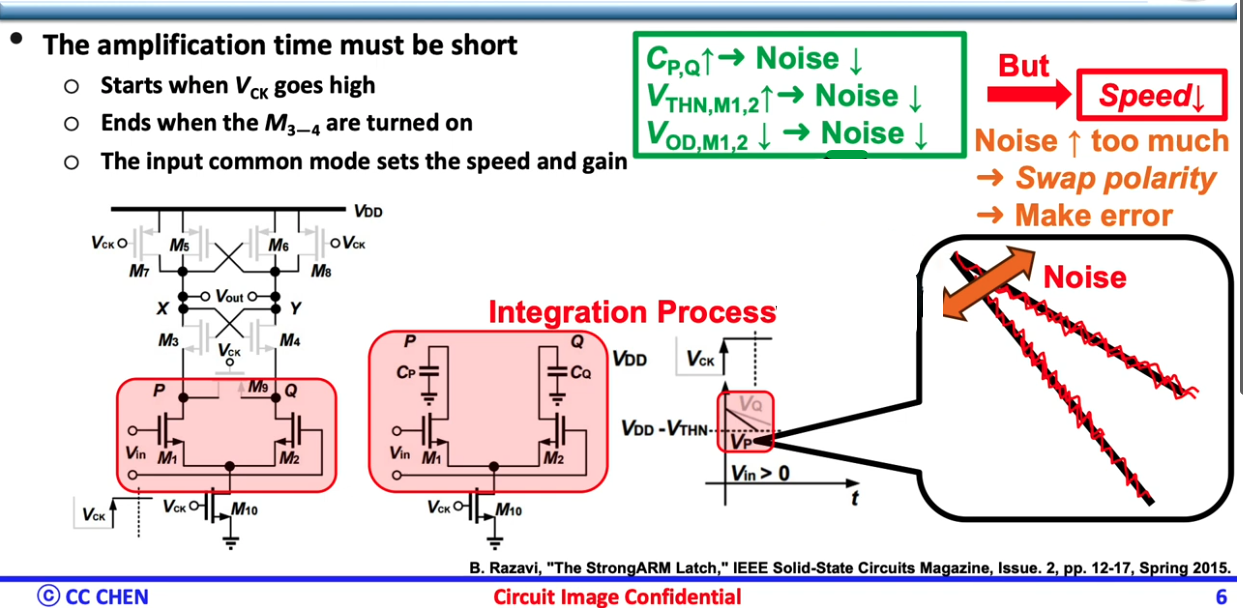
If the input referred offset follows a normal distribution than it is sufficient to apply a single offset voltage to calculate the offset voltage. See details in Razavi, B., The StrongARM Latch [A Circuit for All Seasons], IEEE Solid-State Circuits Magazine, Volume:7, Issue: 2, Spring 2015
Omran, Hesham. (2019). Fast and accurate technique for comparator
offset voltage simulation. Microelectronics Journal. 89.
10.1016/j.mejo.2019.05.004.
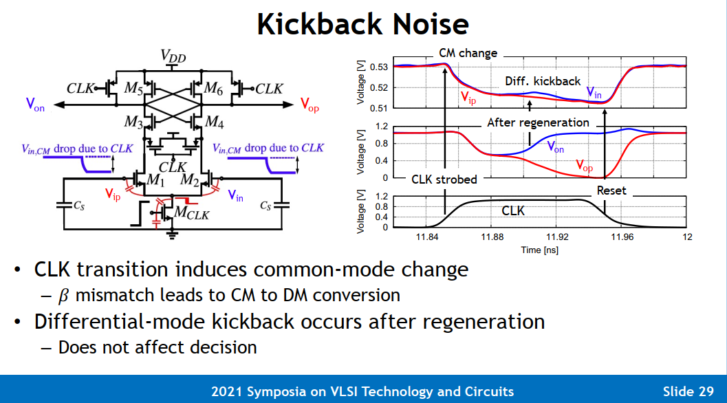
Kickback noise trades with the dimensions of the input
transistors and hence with the offset voltage
affects the comparator's own decision
corrupts the input voltage while it is sensed by other circuits
Tetsuya Iizuka,VLSI2021_Workshop3 "Nyquist A/D Converter Design in
Four Days"
Figueiredo, Pedro & Vital, João. (2006). Kickback noise reduction
techniques for CMOS latched comparators. Circuits and Systems II:
Express Briefs, IEEE Transactions on. 53. 541 - 545.
10.1109/TCSII.2006.875308. [https://sci-hub.se/10.1109/TCSII.2006.875308]
P. M. Figueiredo and J. C. Vital, "Low kickback noise techniques for
CMOS latched comparators," 2004 IEEE International Symposium on Circuits
and Systems (ISCAS), Vancouver, BC, Canada, 2004, pp. I-537 [https://sci-hub.se/10.1109/ISCAS.2004.1328250]
Current mirrors are used between stages to reduce
charge kick back from the logic level swing of the
latch onto the small comparator input capacitors
Mike Shuo-Wei Chen and R. W. Brodersen, "A 6-bit 600-MS/s 5.3-mW
Asynchronous ADC in 0.13-μm CMOS," in IEEE Journal of Solid-State
Circuits, vol. 41, no. 12, pp. 2669-2680, Dec. 2006 [pdf,
slides]
K. Bult and A. Buchwald, "An embedded 240-mW 10-b 50-MS/s CMOS ADC in
1-mm/sup 2/," in IEEE Journal of Solid-State Circuits, vol. 32, no. 12,
pp. 1887-1895, Dec. 1997 [https://sci-hub.st/10.1109/4.643647]
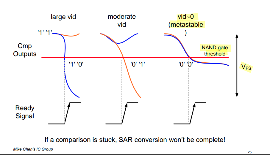
If the comparator can not generate a well-defined logical output in
half of the clock period, we say the circuit is
"metastable"
Mathematical Preliminaries
Relating \(\Phi\) and erf
Error Function (Erf) of the
standard Normal distribution \[
\text{Erf}(x) = \frac{2}{\sqrt{\pi}}\int_0^x e^{-t^2} \mathrm{d}t.
\]Cumulative Distribution Function
(CDF) of the standard Normal distribution \[
\Phi(x) = \frac{1}{\sqrt{2\pi}}\int_{-\infty}^x e^{-z^2/2} \mathrm{d}z.
\]
P. Nuzzo, F. De Bernardinis, P. Terreni and G. Van der Plas, "Noise
Analysis of Regenerative Comparators for Reconfigurable ADC
Architectures," in IEEE Transactions on Circuits and Systems I:
Regular Papers, vol. 55, no. 6, pp. 1441-1454, July 2008 [https://picture.iczhiku.com/resource/eetop/SYirpPPPaAQzsNXn.pdf]
J. Kim, B. S. Leibowitz and M. Jeeradit, "Impulse sensitivity
function analysis of periodic circuits," 2008 IEEE/ACM International
Conference on Computer-Aided Design, 2008, pp. 386-391, doi:
10.1109/ICCAD.2008.4681602. [https://websrv.cecs.uci.edu/~papers/iccad08/PDFs/Papers/05C.2.pdf]
Y. Luo, A. Jain, J. Wagner and M. Ortmanns, "Input Referred
Comparator Noise in SAR ADCs," in IEEE Transactions on Circuits and
Systems II: Express Briefs, vol. 66, no. 5, pp. 718-722, May 2019. [https://sci-hub.se/10.1109/TCSII.2019.2909429]
X. Tang et al., "An Energy-Efficient Comparator With Dynamic Floating
Inverter Amplifier," in IEEE Journal of Solid-State Circuits, vol. 55,
no. 4, pp. 1011-1022, April 2020 [https://sci-hub.se/10.1109/JSSC.2019.2960485]
C. Mangelsdorf, "Metastability: Deeply misunderstood [Shop Talk: What
You Didn’t Learn in School]," in IEEE Solid-State Circuits Magazine,
vol. 16, no. 2, pp. 8-15, Spring 2024
Rabuske, Taimur & Fernandes, Jorge. (2014). Noise-aware
simulation-based sizing and optimization of clocked comparators. Analog
Integr. Circuits Signal Process.. 81. 723-728.
10.1007/s10470-014-0428-4. [https://sci-hub.se/10.1007/s10470-014-0428-4]
Rabuske, Taimur & Fernandes, Jorge. (2016). Charge-Sharing SAR
ADCs for Low-Voltage Low-Power Applications.
10.1007/978-3-319-39624-8.
Masaya Miyahara, Yusuke Asada, Daehwa Paik and Akira Matsuzawa, "A
low-noise self-calibrating dynamic comparator for high-speed ADCs,"
2008 IEEE Asian Solid-State Circuits Conference, Fukuoka,
Japan, 2008 [slides,
paper]
Igor Freire. Symbol Timing Synchronization: A Tutorial [blog,
code]
But the problem here is: "How does the receiver know the ideal
sampling instants?". The solution is "someone has to supply those
ideal sampling instants". A symbol time
recovery circuit is used for this purpose.
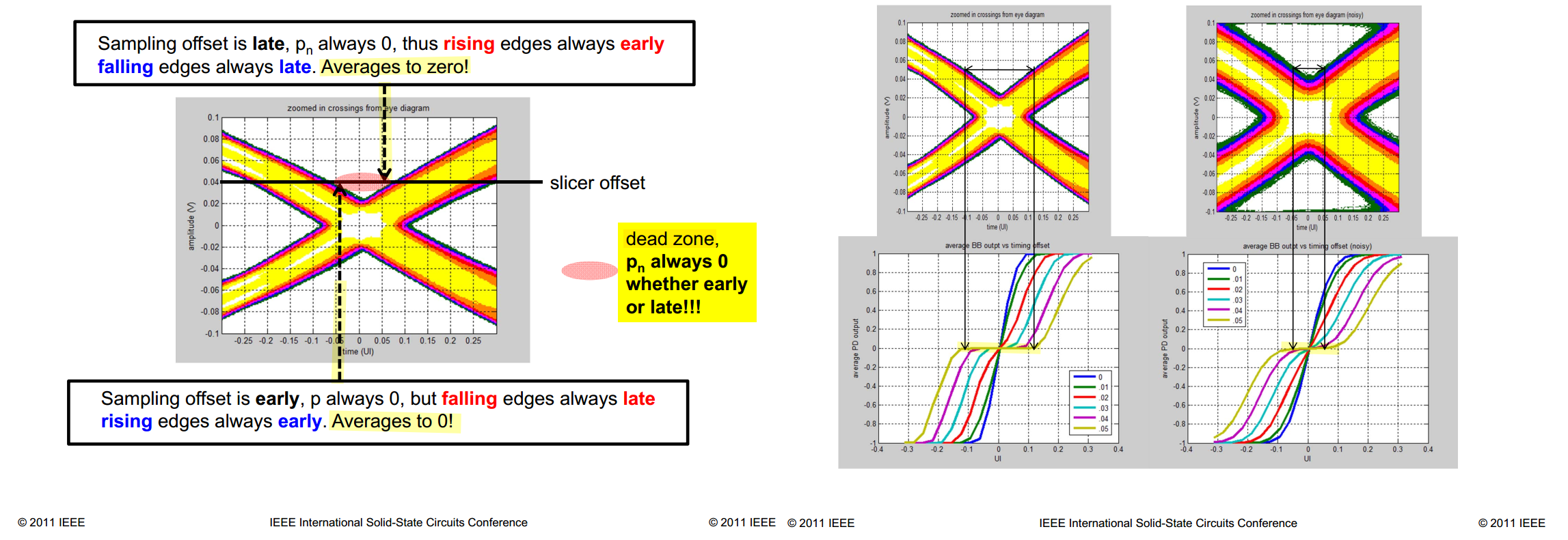
Early/Late Symbol Recovery algorithm
non-decision-directed timing estimator exploits the
symmetry properties of the signal
If the Early Sample = Late Sample : The
peak occurs at the on-time sampling instant \(T\). No adjustment in the timing is
needed.
If |Early Sample| > |Late Sample| :
Late timing, the sampling time is offset so that the next symbol is
sampled \(T-\delta/2\) seconds after
the current sampling time.
If |Early Sample| < |Late Sample| :
Early timing, the sampling time is offset so that the next symbol is
sampled \(T+\delta/2\) seconds after
the current sampling time.
David Johns. ECE1392H - Integrated Circuits for Digital
Communications - Fall 2001: [Timing
Recovery]
Dither in Quantized Zero Crossing Detection (QZCD)
(so-called 'Bang Bang' Phase Detector)
Mueller and Muller
Timing Synchronization
K. Mueller and M. Muller, "Timing Recovery in Digital Synchronous
Data Receivers," in IEEE Transactions on Communications, vol.
24, no. 5, pp. 516-531, May 1976 [pdf]
C.-P. Tzeng, D. Hodges and D. Messerschmitt, "Timing Recovery in
Digital Subscriber Loops Using Baud-Rate Sampling," in IEEE Journal
on Selected Areas in Communications, vol. 4, no. 8, pp. 1302-1311,
November 1986 [pdf]
H. Meyr, M. Moeneclaey, and S. A. Fechtel. "Digital Communication
Receivers: Synchronization, Channel Estimation, and Signal Processing."
Wiley [pdf]
T. Musah and A. Namachivayam, "Robust Timing Error Detection for
Multilevel Baud-Rate CDR," in IEEE Transactions on Circuits and Systems
I: Regular Papers, vol. 69, no. 10, pp. 3927-3939, Oct. 2022 [https://sci-hub.jp/10.1109/TCSI.2022.3191740]
Fulvio Spagna, CICC2018 Clock and Data Recovery Systems [pdf]
TODO 📅
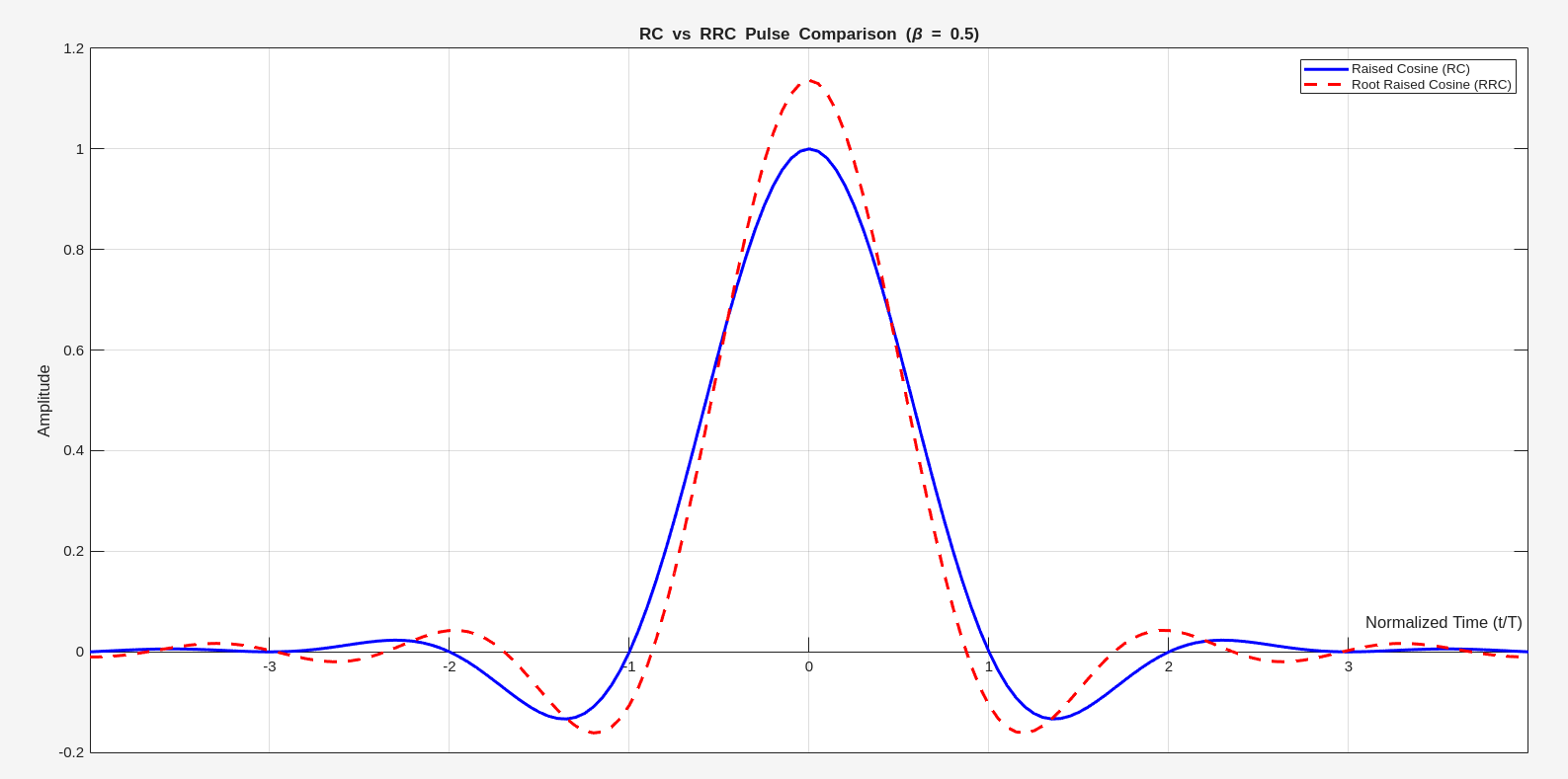
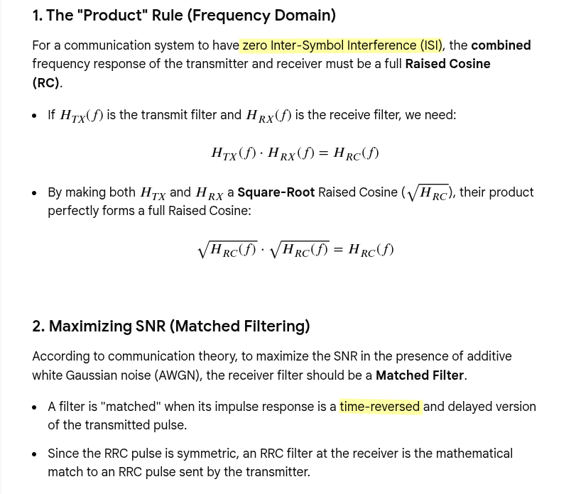
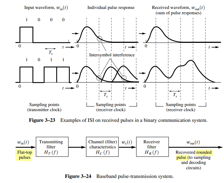
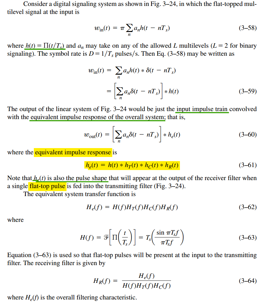
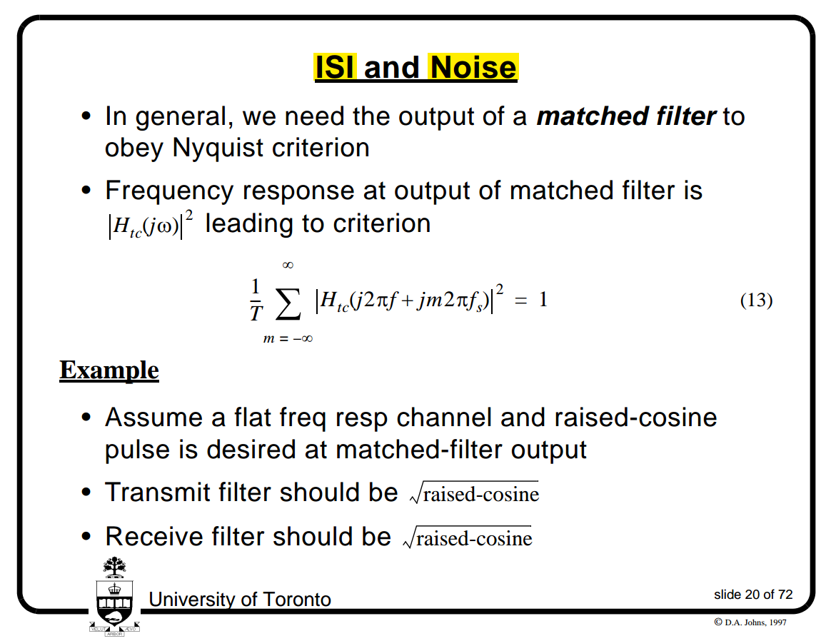
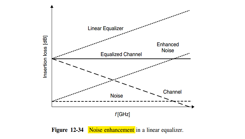
Intersymbol Interference
(ISI)
L.W. Couch, Digital and Analog CommunicationSystems, 8th Edition, Pearson, 2013. [pdf]
Nyquist discovered three different methods for pulse shaping that
could be used to eliminate ISI
Nyquist's First Method (Zero ISI): physically
unrealizable (i.e., the impulse response would be noncausal and of
infinite duration), inaccurate sync will cause ISI
Nyquist's second method: allows some ISI to be
introduced in a controlled way
Nyquist's third method: area under the \(h_e(t)\) pulse within the desired symbol
interval, \(T_s\), is not zero, but the
areas under \(h_e(t)\) in adjacent
symbol intervals are zero
Nyquist Criterion & Pulses
David A. Johns, ECE1392H - Integrated Circuits for Digital
Communications - Fall 2001 [System
Overview]
Matched-Filter (MF)
David A. Johns, ECE1392H - Integrated Circuits for Digital
Communications - Fall 2001 [System
Overview]
David A. Johns, ECE1392H - Integrated Circuits for Digital
Communications - Fall 2001 [Introduction]
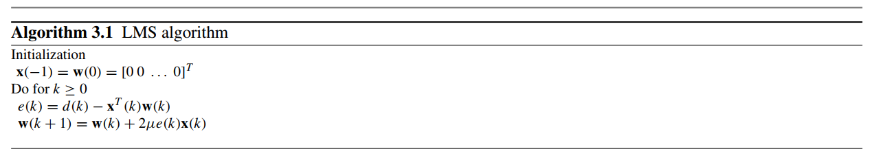
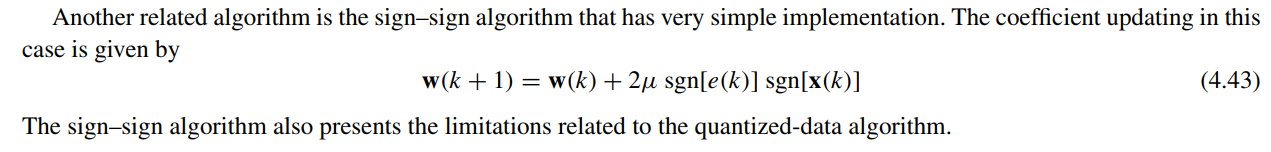
LMS & its
Quantized-Error Algorithms
Bruno Lima, Adaptive filtering in Python Implementations based on
Adaptive Filtering: Algorithms and Practical Implementation (Paulo S. R.
Diniz). [https://github.com/BruninLima/PydaptiveFiltering]
Sen M. Kuo. Real-Time Digital Signal Processing: Fundamentals,
Implementations and Applications, 3rd Edition. John Wiley & Sons
2013
Stankovic, Ljubisa. (2015). Digital Signal Processing with Selected
Topics.
Paulo S. R. Diniz, Adaptive Filtering: Algorithms and Practical
Implementation, 5th edition [pdf],
[matlab],
[python]
B. Farhang-Boroujeny (2013), Adaptive Filters: Theory and
Applications (2nd ed.). John Wiley & Sons, Inc.
Simon O. Haykin (2014), "Adaptive Filter Theory" Prentice-Hall, Inc.
5rd edition
A. Chan Carusone and D. A. Johns, "Analog Filter Adaptation Using a
Dithered Linear Search Algorithm," IEEE Int. Symp. Circuits and
Syst., May 2002. [PDF], [Slides]
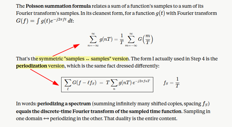
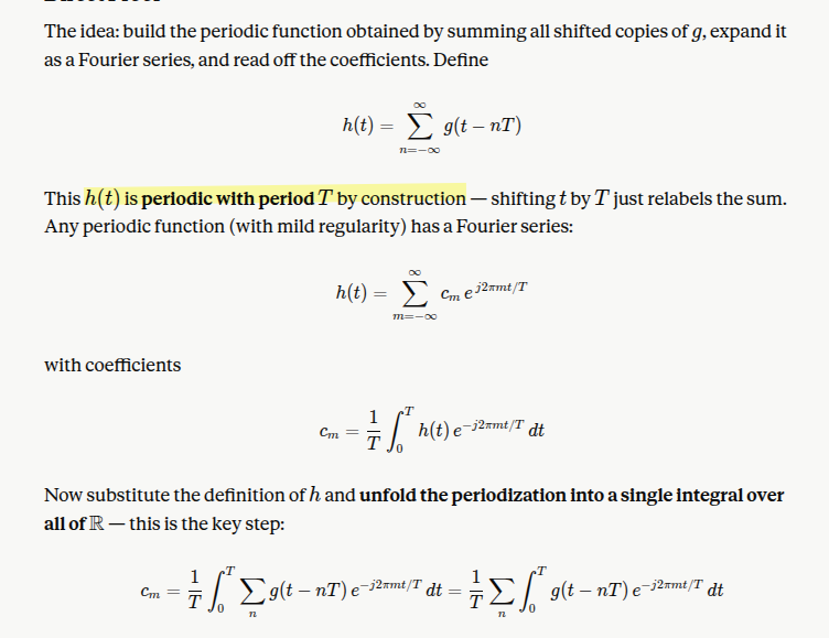
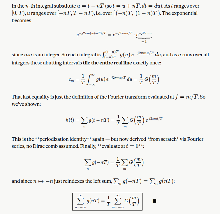
Let the periodic waveform \(w(t)\),
with period \(T_0=2\pi/\omega_0\), have
the complex Fourier series \[
w(t)=\sum_{\ell=-\infty}^{\infty}W[\ell]e^{j\ell\omega_0t}.
\] We want the Fourier coefficients of \[
w(t)\sin(\omega_0t)
\quad\text{and}\quad
w(t)\cos(\omega_0t).
\]
Multiplication by \(\sin(\omega_0t)\)
Use \[
\sin(\omega_0t)
=
\frac{e^{j\omega_0t}-e^{-j\omega_0t}}{2j}.
\] Then \[
\begin{aligned}
w(t)\sin(\omega_0t)
&=
\left(\sum_{\ell=-\infty}^{\infty}
W[\ell]e^{j\ell\omega_0t}\right)
\frac{e^{j\omega_0t}-e^{-j\omega_0t}}{2j}
\\[4pt]
&=
\frac{1}{2j}
\sum_{\ell=-\infty}^{\infty}
W[\ell]
\left[
e^{j(\ell+1)\omega_0t}
-
e^{j(\ell-1)\omega_0t}
\right].
\end{aligned}
\] Now collect the coefficient multiplying \(e^{jk\omega_0t}\).
For the first term, \[
k=\ell+1
\quad\Longrightarrow\quad
\ell=k-1,
\] so its coefficient is \(W[k-1]\).
For the second term, \[
k=\ell-1
\quad\Longrightarrow\quad
\ell=k+1,
\] so its coefficient is \(W[k+1]\).
Therefore, \[
\boxed{
w(t)\sin(\omega_0t)
=
\sum_{k=-\infty}^{\infty}
\frac{W[k-1]-W[k+1]}{2j}
e^{jk\omega_0t}
}
\] and the Fourier coefficient is \[
\color{blue}\boxed{
\left[w(t)\sin(\omega_0t)\right]_k
=
\frac{W[k-1]-W[k+1]}{2j}.
}
\]
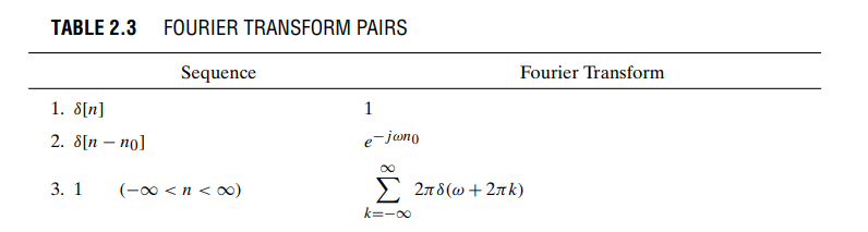
DFT \(X[k]\) is a
sampled version of the DTFT \(X(e^{j\hat{\omega}})\), with the \(k\)-th sampled digital frequency, \(\hat{\omega}_k = \frac{2\pi k}{N}\)\[
\boxed{X[k] = X(e^{j\hat{\omega}})\bigg|_{\hat{\omega}=\hat{\omega}_k},
\qquad
\hat{\omega}_k = \frac{2\pi k}{N},
\qquad
k=0,1,\dots,N-1}
\]
DTFT vs DFT
Schuller, Gerald. 2026. Multirate Signal Processing with Examples in
Python. Cham: Springer Nature Switzerland.
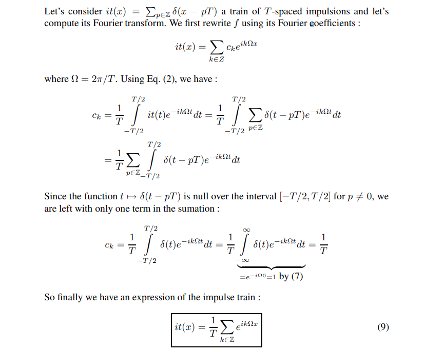
impulse train
CTFT:
using time-sampling property
DTFT:
Given \(x[n]=\sum_{k=-\infty}^{\infty}\delta(n-k)\)
where \(H(j\omega)\), \(H(e^{j\hat{\omega}})\) is frequency
response of continuous-time systems and
discrete-time systems, which is the function of \(\omega\) and \(\hat{\omega}\)\[\begin{align}
H(j\omega) &= \int_{-\infty}^{+\infty}h(t)e^{-j\omega t}dt \\ \\
H(e^{j\hat{\omega}}) &=
\sum_{n=-\infty}^{+\infty}h[n]e^{-j\hat{\omega} n}
\end{align}\]
The frequency response of discrete-time LTI systems
is always a periodic function of the frequency variable
\(\hat{\omega}\) with period \(2\pi\)
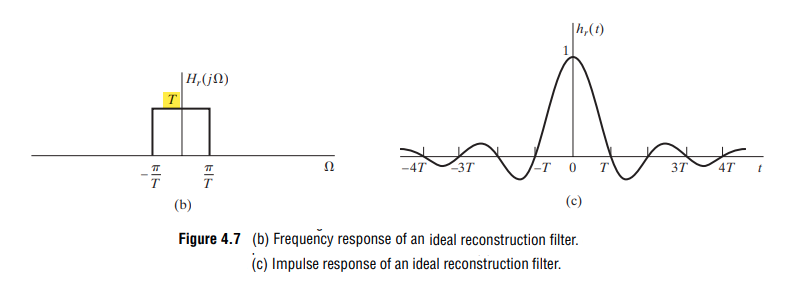
Sampling Theorem
time-sampling theorem: applies to bandlimited
signals
spectral sampling theorem: applies to
timelimited signals
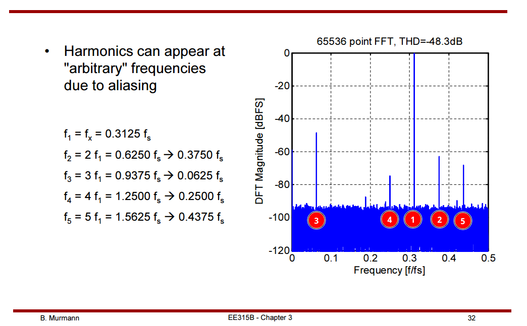
Aliasing
Given below sequence \[
X[n] =A e^{j\omega T_s n}
\]
whileTrue: for signN, signFsig in product([-1, 1], [-1, 1]): fdisp_n = signN*N*fs + signFsig*fsig if fdisp_n >= 0and fdisp_n < fs/2: fdisp = fdisp_n print(f"{fsig:.4f} is indistinguishable from {fdisp:.4f}, which is {'+'if signN>0else'-'}{N}{'+'if signFsig>0else'-'}{fsig:.4f}") return fdisp N += 1 if N > 100: break returnNone
for i inrange(1,6): samplealiasing(0.3125*i)
# 0.3125 is indistinguishable from 0.3125, which is -0 + 0.3125 # 0.6250 is indistinguishable from 0.3750, which is +1 - 0.6250 # 0.9375 is indistinguishable from 0.0625, which is +1 - 0.9375 # 1.2500 is indistinguishable from 0.2500, which is -1 + 1.2500 # 1.5625 is indistinguishable from 0.4375, which is +2 - 1.5625
# inspired by https://github.com/bmurmann/MEAD2026/blob/main/tb_boot_bottom_4.ipynb
defsamplealiasing(fsig, fs=1): fdisp = None fsig_wrap = fsig % fs if fsig_wrap > fs/2: fdisp = fs - fsig_wrap else: fdisp = fsig_wrap print(f"{fsig:.4f} is indistinguishable from {fdisp:.4f}") return fdisp
for i inrange(1,6): samplealiasing(0.3125*i)
# 0.3125 is indistinguishable from 0.3125 # 0.6250 is indistinguishable from 0.3750 # 0.9375 is indistinguishable from 0.0625 # 1.2500 is indistinguishable from 0.2500 # 1.5625 is indistinguishable from 0.4375
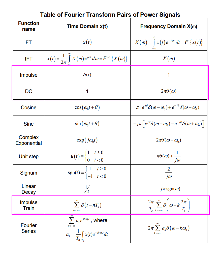
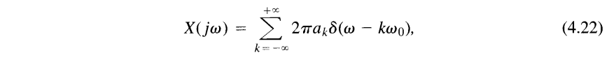
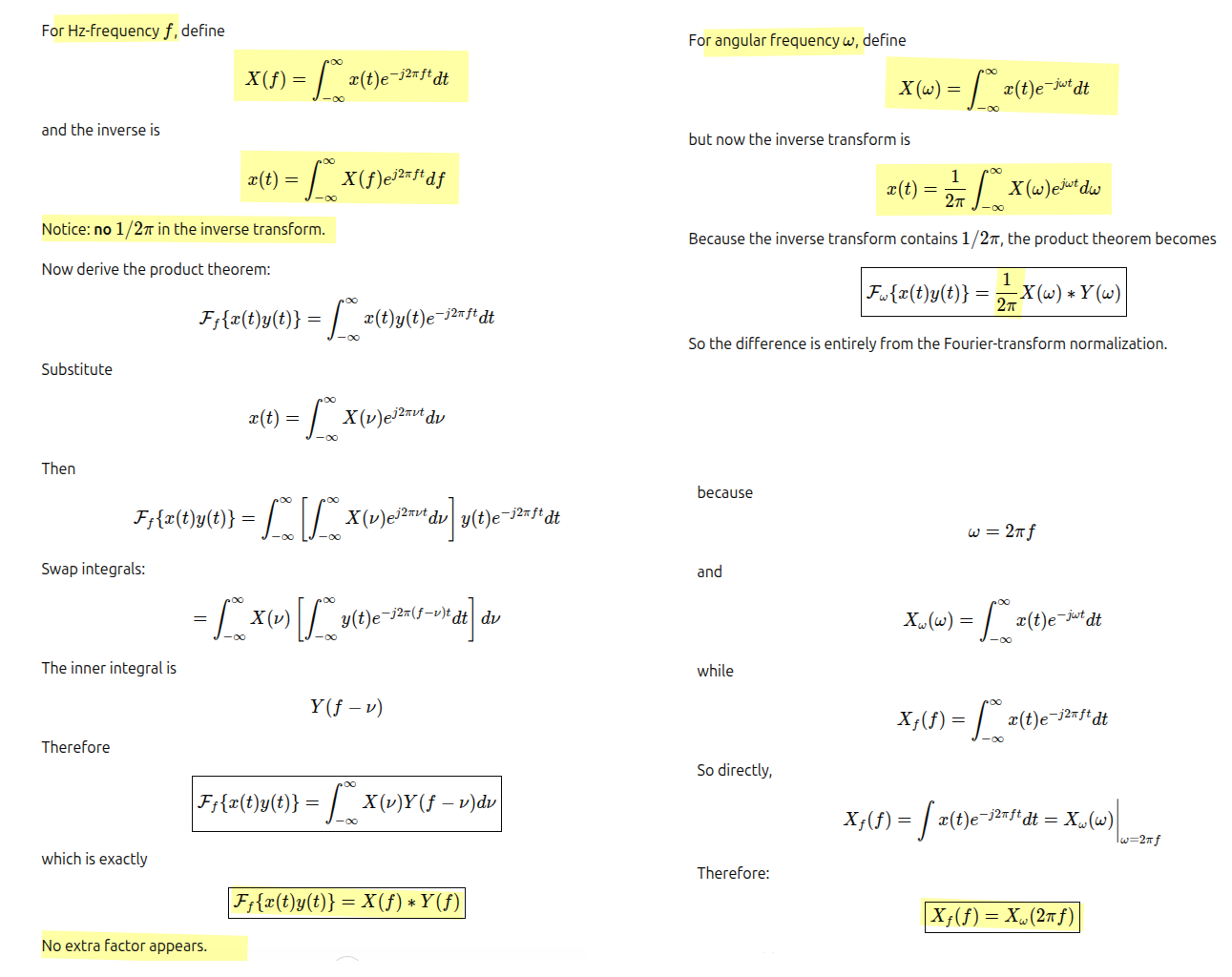
CTFS & CTFT
Fourier transform of a periodic signal with Fourier series
coefficients \(\{a_k\}\) can be
interpreted as a train of impulses occurring at the
harmonically related frequencies and for which the area of the impulse
at the \(k\)th harmonic frequency \(k\omega_0\) is \(2\pi\) times the \(k\)th Fourier series coefficient \(a_k\)
inverse CTFT & inverse DTFT
time domain
frequency domain
inverse CTFT
\(\delta(t)\)
\(\int_{\infty}d\omega\)
inverse DTFT
\(\delta[n]\)
\(\int_{2\pi}d\hat{\omega}\)
inverse CTFT shall integral from \(-\infty\) to \(+\infty\) to obtain \(\delta(t)\) in time domain, e.g., \(x_s(t)\) impulse train
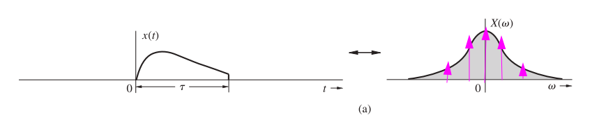
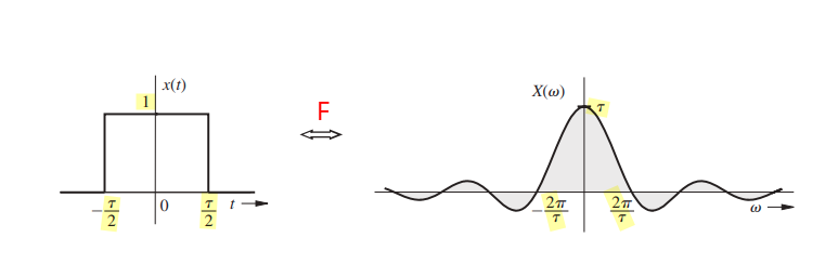
Consider the periodic pulse function \(x_T(t) = \Pi_T \left( \frac{t}{T_p}
\right)\)
Fourier Series Coefficients is \[
c_n = \frac{T_p}{T} \operatorname{sinc} \left( \frac{n T_p}{T} \right)
\] The Fourier Transform of the function is \[
X_T(\omega) = \sum_{n=-\infty}^{+\infty} c_n 2\pi \delta(\omega -
n\omega_0)
\]
spectral sampling
spectral sampling by \(\omega_0\),
and \(\frac{2\pi}{\omega_0} \gt \tau\)\[
X_{n\omega_0}(\omega) =
\sum_{n=-\infty}^{\infty}X(n\omega_0)\delta(\omega - n\omega_0)
\] Periodic repetition of \(x(t)\) is \[
x_{n\omega_0}(t) = \frac{1}{\omega_0}\sum_{n=-\infty}^{\infty}x(t
-n\frac{2\pi}{\omega_0})=\frac{T_0}{2\pi}\sum_{n=-\infty}^{\infty}x(t
-nT_0)
\]
Then, if \(x_{T_0} (t)\), a periodic
signal formed by repeating \(x(t)\)
every \(T_0\) seconds (\(T_0 \gt \tau\)), its CTFT is \[
X_{T_0}(\omega) = \frac{2\pi}{T_0} \cdot X_{n\omega_0}(\omega) =
\frac{2\pi}{T_0}\sum_{n=-\infty}^{\infty}X(n\omega_0)\delta(\omega -
n\omega_0)
\] Then \(x_{T_0} (t)\) can be
expressed with inverse CTFT as \[\begin{align}
x_{T_0} (t) &=
\frac{1}{2\pi}\int_{-\infty}^{\infty}X_{T_0}(\omega)e^{j\omega t}d\omega
\\
&= \frac{1}{T_0}\sum_{n=-\infty}^{\infty}X(n\omega_0)e^{jn\omega_0
t} =\sum_{n=-\infty}^{\infty}\frac{1}{T_0}X(n\omega_0)e^{jn\omega_0 t}
\end{align}\]
i.e. the coefficients of the Fourier series for \(x_{T_0} (t)\) is \(D_n =\frac{1}{T_0}X(n\omega_0)\)
alternative method by direct Fourier series
Why DFT ?
We can use DFT to compute DTFT samples and CTFT samples
\[
\overline{x}(t) = \sum_{n=0}^{N_0-1}x(nT)\delta(t-nT)
\] applying the Fourier transform yieds \[
\overline{X}(\omega) = \sum_{n=0}^{N_0-1}x[n]e^{-jn\omega T}
\] But \(\overline{X}(\omega)\),
the Fourier transform of \(\overline{x}(t)\) is \(X(\omega)/T\), assuming negligible
aliasing. Hence, \[
X(\omega) = T\overline{X}(\omega) = T\sum_{n=0}^{N_0-1}x[n]e^{-jn\omega
T}
\] and \[
X(k\omega_0) = T\sum_{n=0}^{N_0-1}x[n]e^{-jn k\omega_0 T}
\] with \(\hat{\omega}_0 = \omega_0
T\)\[
X(k\omega_0) = T\sum_{n=0}^{N_0-1}x[n]e^{-jn k\hat{\omega}_0}
\]i.e. the relationship between CTFT and DFT is \(X(k\omega_0) = T\cdot X[k]\), DFT is a tool
for computing the samples of CTFT
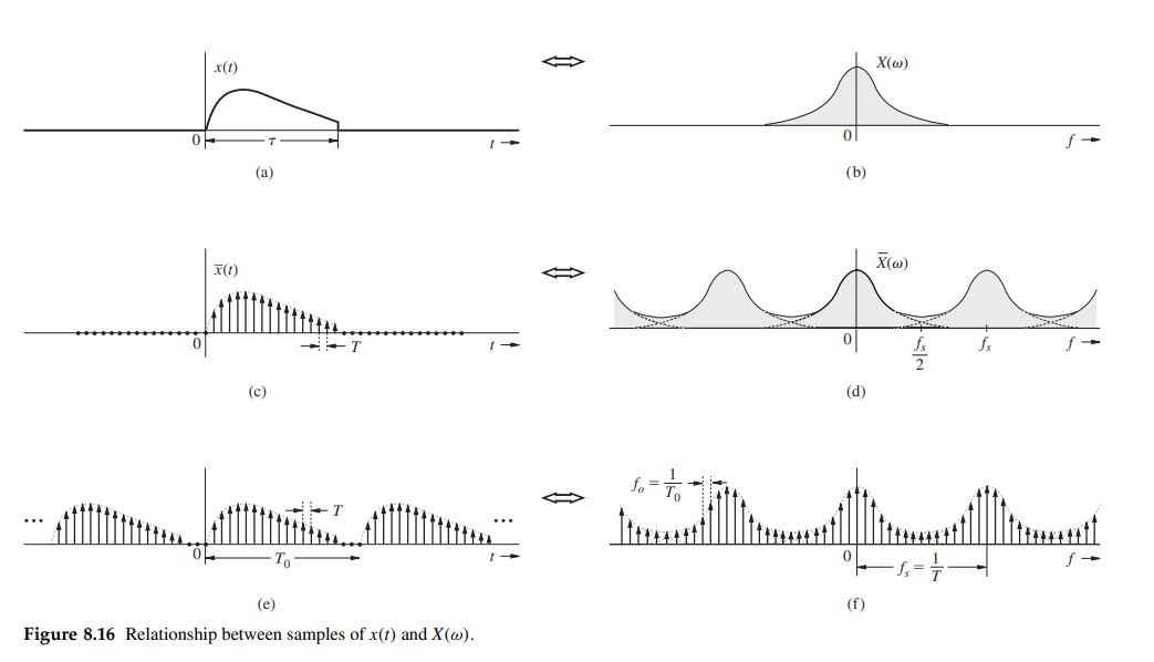
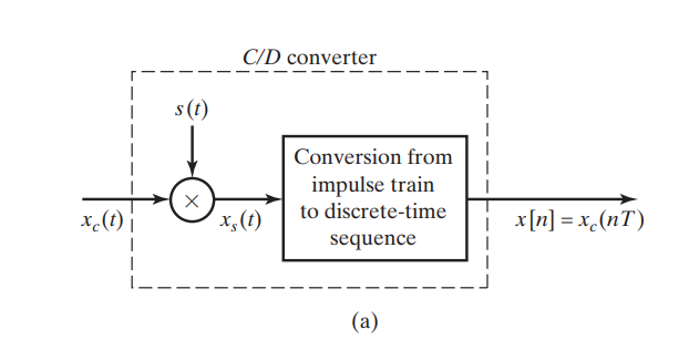
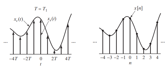
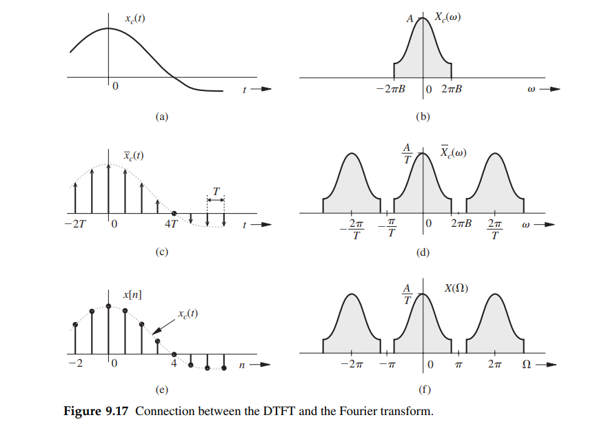
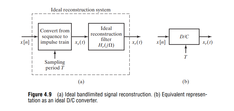
C/D
Sampling with a periodic impulse train, followed by conversion to a
discrete-time sequence
The periodic impulse train is \[
s(t) = \sum_{n=-\infty}^{\infty}\delta(t-nT)
\]\(x_s(t)\) can be expressed
as \[
x_s(t) = \sum_{n=-\infty}^{\infty}x_c(nT)\delta(t-nT)
\] i.e., the size (area) of the impulse at sample time
\(nT\) is equal to the value of the
continuous-time signal at that time.
\(x_s(t)\) is, in a sense, a
continuous-time signal (specifically, an impulse train)
samples of \(x_c(t)\) are represented by
finite numbers in \(x[n]\)
rather than as the areas of impulses, as with \(x_s(t)\)
Frequency-Domain
Representation of Sampling
The relationship between the Fourier transforms of the input and the
output of the impulse train modulator \[
X_s(j\omega) = \frac{1}{T}\sum_{k=-\infty}^{\infty}X_c(j(\omega
-k\omega_s))
\] where \(\omega_s\) is the
sampling frequency in radians/s
\(X(e^{j\hat{\omega}})\), the
discrete-time Fourier transform (DTFT) of the sequence \(x[n]\), in terms of \(X_s(j\omega)\) and \(X_c(j\omega)\)
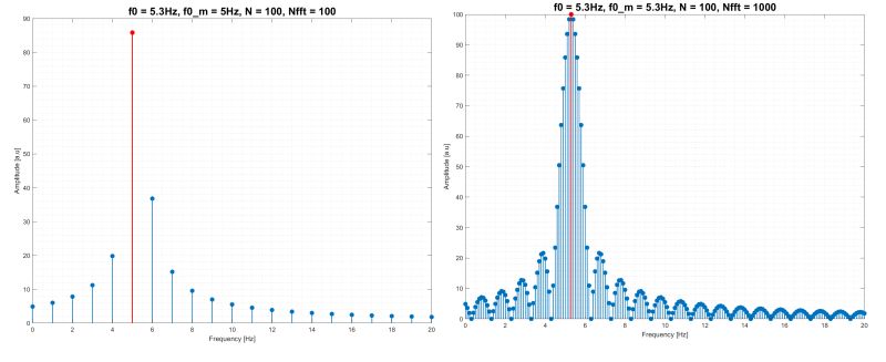
Zero padding improves frequency grid resolution, not
spectral resolution
A smoother spectrum is not more information — it is better
interpolation of the same information.
To truly improve spectral resolution, you must observe the signal
longer (increase N).
Gotcha
A remarkable fact of linear systems is that the complex
exponentials are eigenfunctions of a linear
system, as the system output to these inputs equals the input multiplied
by a constant factor.
Both amplitude and phase may change
but the frequency does not change
For an input \(x(t)\), we can
determine the output through the use of the convolution integral, so
that with \(x(t) = e^{st}\)\[\begin{align}
y(t) &= \int_{-\infty}^{+\infty}h(\tau)x(t-\tau)d\tau \\
&= \int_{-\infty}^{+\infty} h(\tau) e^{s(t-\tau)}d\tau \\
&= e^{st}\int_{-\infty}^{+\infty} h(\tau) e^{-s\tau}d\tau \\
&= e^{st}H(s)
\end{align}\]
Take the input signal to be a complex exponential of the form \(x(t)=Ae^{j\phi}e^{j\omega t}\)
The real cosine signal is actually composed of two
complex exponential signals: one with positive
frequency and the other with negative \[
cos(\omega t + \phi) = \frac{e^{j(\omega t + \phi)} + e^{-j(\omega t +
\phi)}}{2}
\]
The sinusoidal response is the sum of the complex-exponential
response at the positive frequency \(\omega\) and the response at the
corresponding negative frequency \(-\omega\) because of LTI systems's
superposition property
input: \[\begin{align}
x(t) &= A cos(\omega t + \phi) \\
&= \frac{1}{2}Ae^{\phi}e^{\omega t} +
\frac{1}{2}Ae^{-\phi}e^{-\omega t}
\end{align}\]
J. Zhong, Y. Zhu, S. -W. Sin, S. -P. U and R. P. Martins, "Thermal
and Reference Noise Analysis of Time-Interleaving SAR and
Partial-Interleaving Pipelined-SAR ADCs," in IEEE Transactions on
Circuits and Systems I: Regular Papers, vol. 62, no. 9, pp. 2196-2206,
Sept. 2015 [https://sci-hub.st/10.1109/TCSI.2015.2452331]
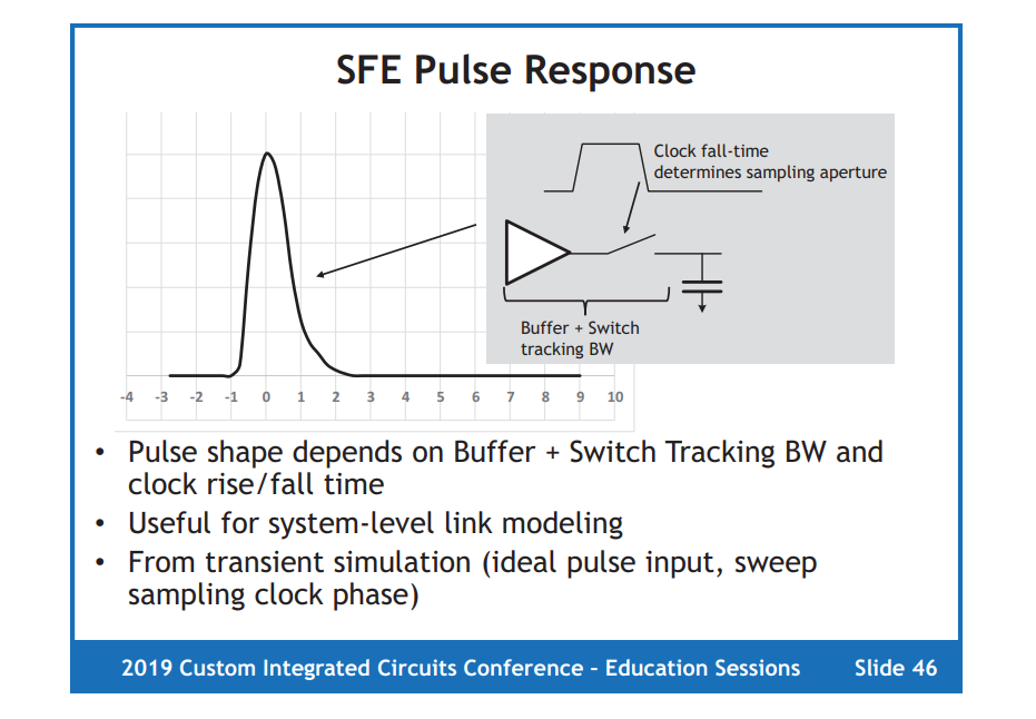
sweep the setup time between ideal pulse input and clock, sample the
output of SFE at falling edge
sample-by-sample
3rd harmonic
bit-by-bit
The amplitude of the reference ripple is code-dependent as it is
correlated with switching energy in each bit cycling
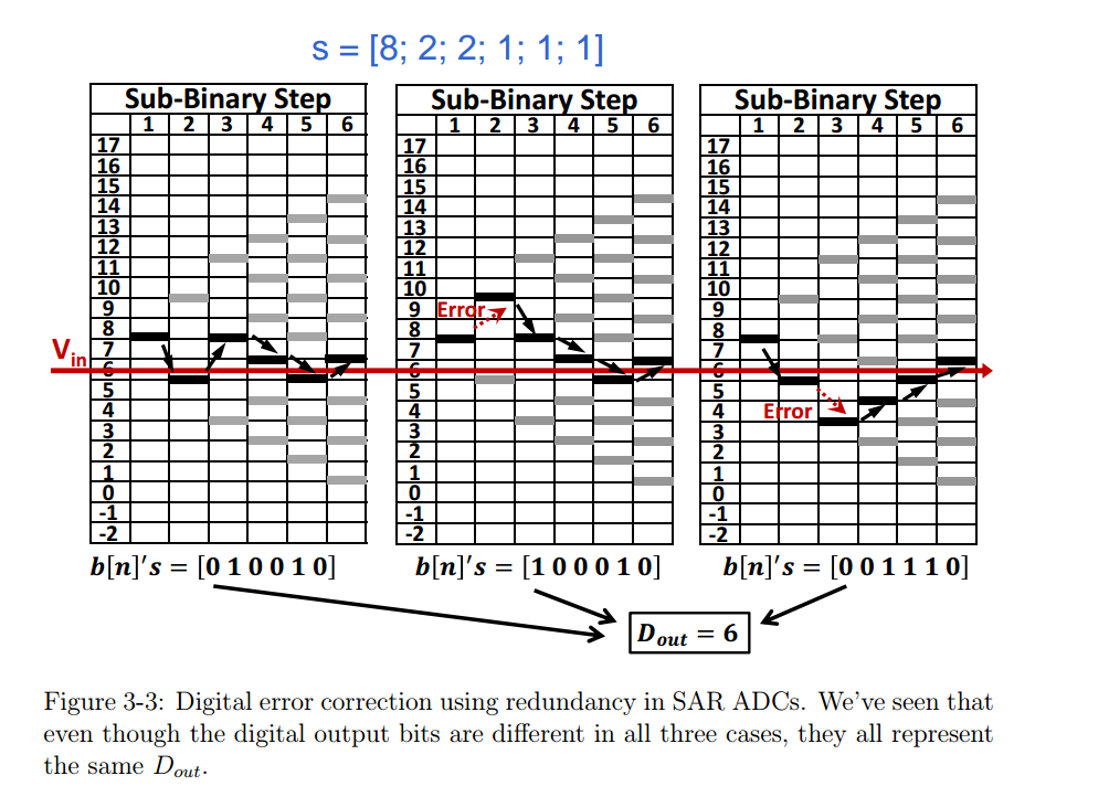
Redundancy
decision level
final digital output for an \(N\)-bit \(M\)-step ADC can be calculated \[
D_{out} = s(M) + \sum_{i=1}^{M-1}(2\cdot b[i] - 1)\times s(i) + (b[0]
-1)\cdot s(1)
\]
i
M
M-1
M-2
...
2
1
0
b[i]
b[M-1]
b[M-2]
...
b[2]
b[1]
b[0]
s[i]
s(M)
s(M-1)
s(M-2)
...
s(2)
s(1)
track the decision level
For \(N\)-bit binary weighted
algorithm,\(N=M\) and \(s(i)=2^{i-1}\), where \(i\in \{N, N-1,...,2,1 \}\)
For the \(n\)th output bit, once a
decision is made, the next decision level will either move up or down by
the step size of \(s(n − 1)\)
If this decision is erroneous, then the sum of the follow-on step
sizes, \(s(n − 2)\), \(s(n − 3)\), ..., \(s(1)\), must be large enough and exceed the
value of the current step size to counteract this mistake
The exceeded amount is the tolerance window for that decision
level
When the ADC is designed with a fixed radix, \(\alpha\) and the required number of
conversion steps, \(M\)
the sum of all the step sizes \(s_{tot}\)\[
s_{tot} = \sum_{k=0}^{M-1} s_0 \alpha^k = s_0\frac{\alpha^M-1}{\alpha-1}
\]
where \(s(i)\) is step size and
\(i \in [0, 1, 2, M-1]\)
The effective number of bits, \(N\),
can be calculated \[
N \leq \log 2\left(\frac{s_{tot} + s_0}{s_0}\right) =
\frac{\alpha^M+\alpha-2}{\alpha-1}
\]
Speed Benefit
TODO 📅
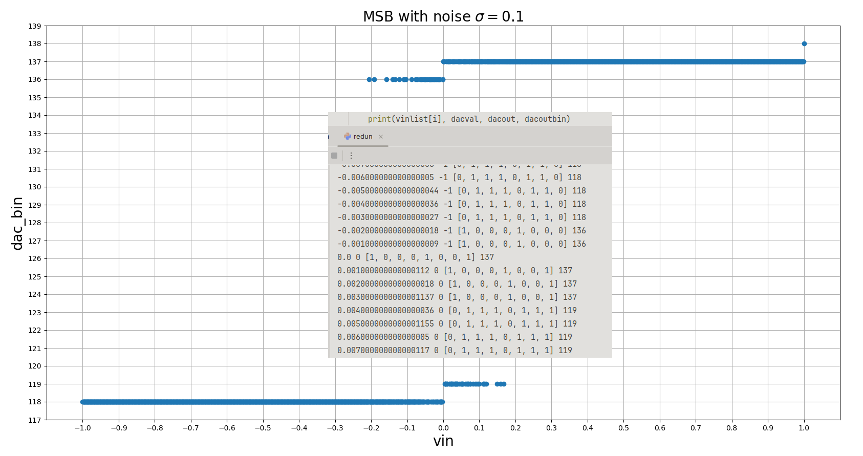
MSB with noise simualtion
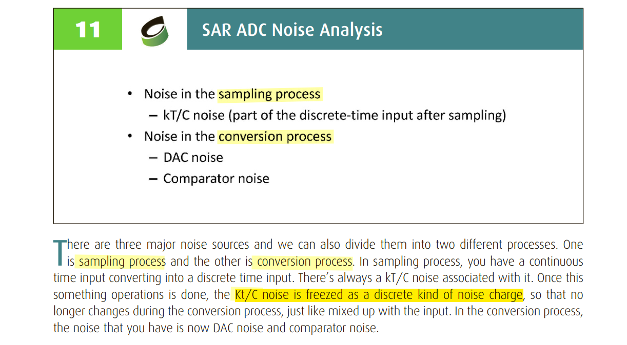
SAR ADC Noise Analysis
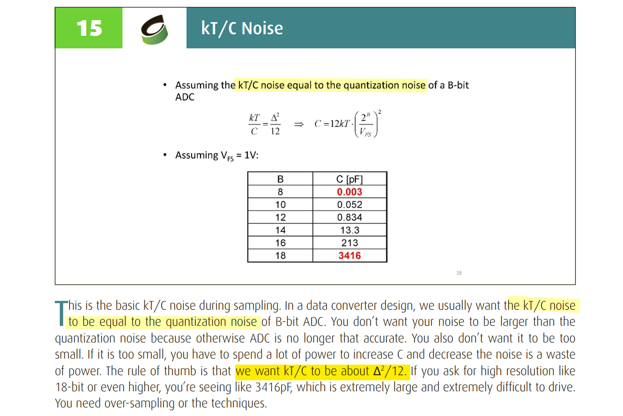
kT/C Noise in sampling
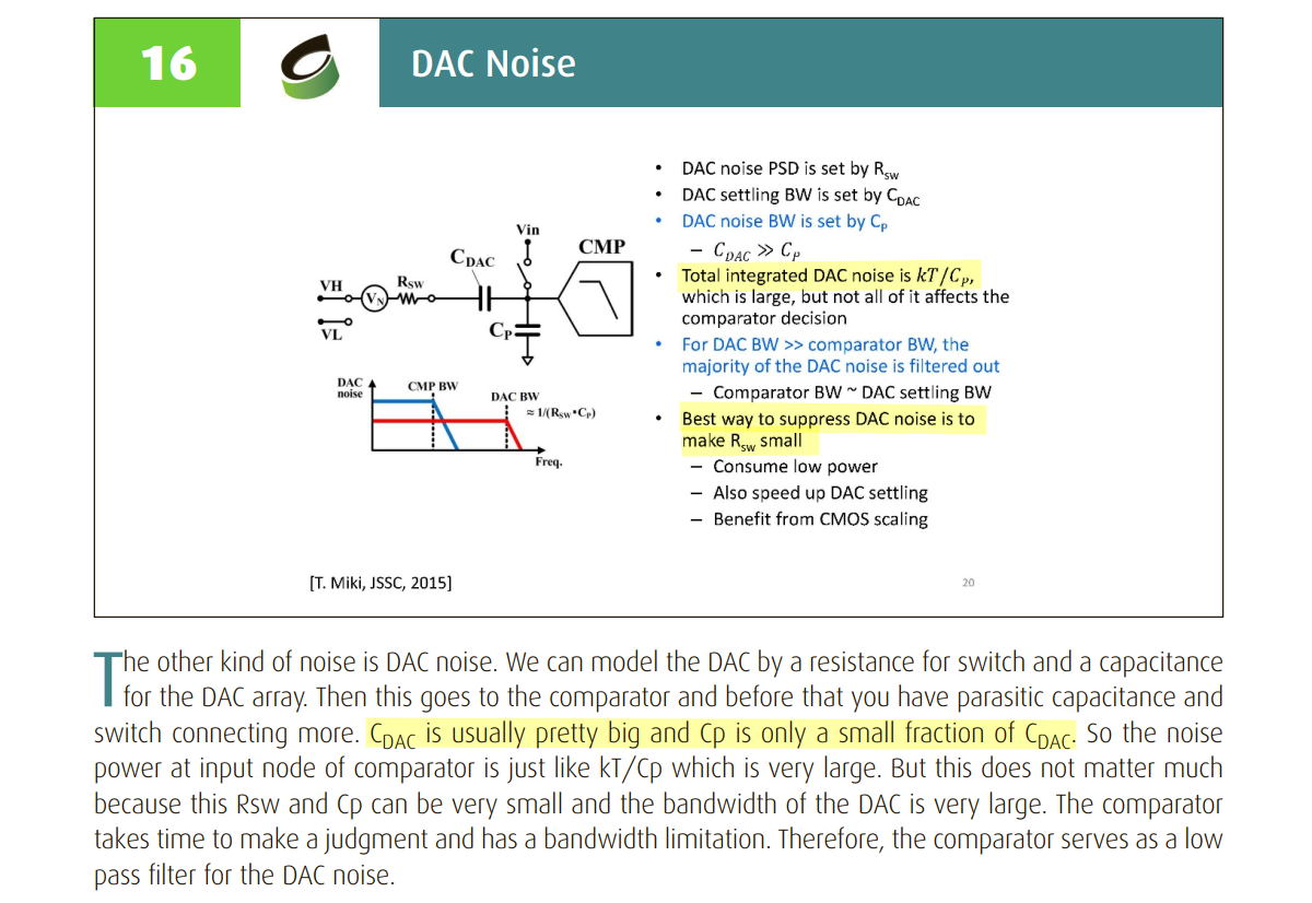
DAC Noise in conversion
T. Miki et al., "A 4.2 mW 50 MS/s 13 bit CMOS SAR ADC With SNR and
SFDR Enhancement Techniques," in IEEE Journal of Solid-State Circuits,
vol. 50, no. 6, pp. 1372-1381, June 2015 [https://sci-hub.jp/10.1109/JSSC.2015.2417803]
Comparator Noise in
conversion
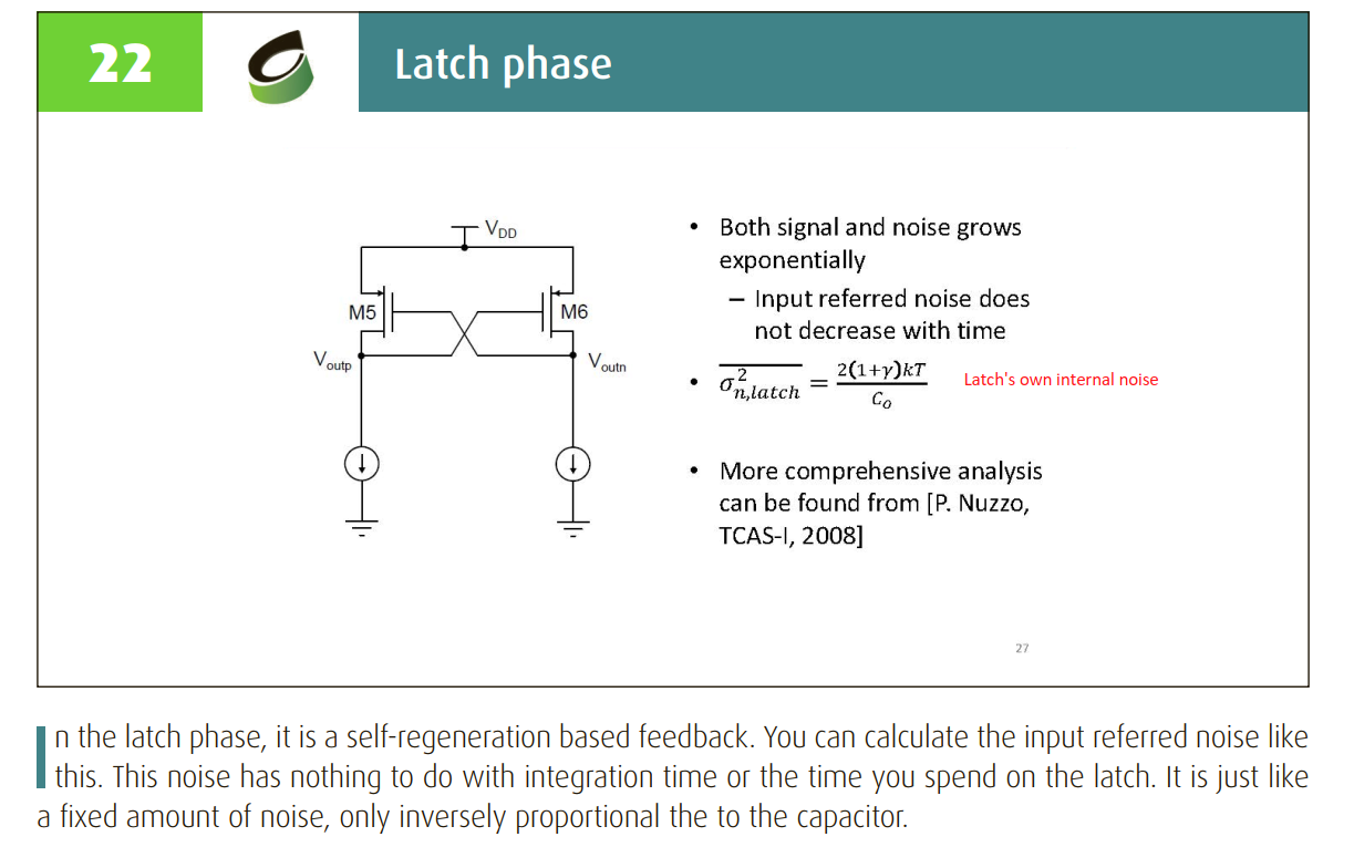
noise analysis for dynamic integrator
noise analysis for latch phase
P. Nuzzo, F. De Bernardinis, P. Terreni and G. Van der Plas, "Noise
Analysis of Regenerative Comparators for Reconfigurable ADC
Architectures," in IEEE Transactions on Circuits and Systems I:
Regular Papers, vol. 55, no. 6, pp. 1441-1454, July 2008
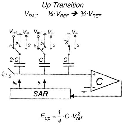
CDAC
The charge redistribution capacitor network is used to
sample the input signal and serves as a digital-to-analog converter
(DAC) for creating and subtracting reference voltages
inverse Laplace Transform is \(V_y(t) =
\frac{C_1}{C_1+C_2}\left(1 - e^{-t/\tau}\right)\)
\(V_x(t)\) and \(V_y(t)\) prove that the settling time is
same
\(\tau = R\frac{C_1C_2}{C_1+C_2}\),
which means usually worst for MSB capacitor (largest)
both \(\tau\) and \(\Delta V\) are the maximum
A popular way to improve the settling behavior, again, is to employ
unit-element DACs that statistically reduce the switching activities,
which, unfortunately, exhibits unnecessary complications to the power,
area and speed tradeoffs of the design
That make sense, charge redistribution consume
energy
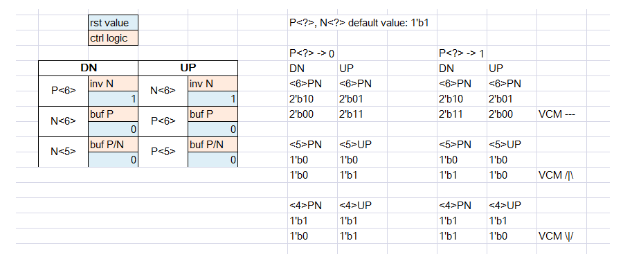
CDAC structure
CDAC with constant common-mode voltage
Comparator
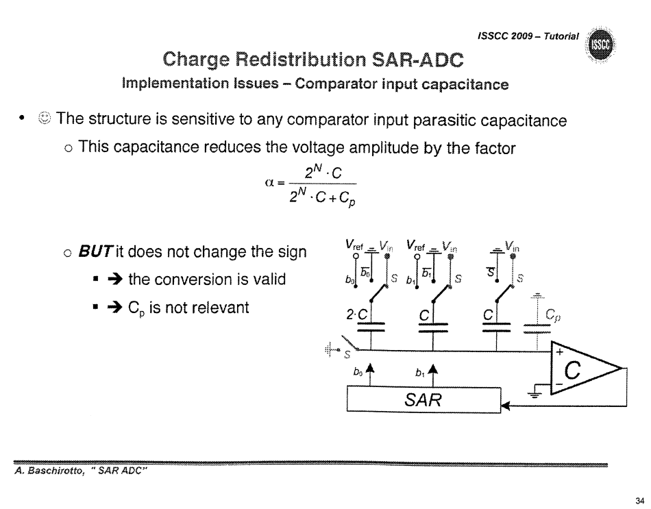
Comparator input cap effect
\[
-V_{in}\cdot 2^N C = V_c (2^N C + C_p)
\] Then \(V_c = -\frac{2^N C}{2^N C +
C_p}V_{in}\), i.e. this capacitance reduce the voltage amplitude
by the factor
During conversion \[\begin{align}
V_c &= -\frac{2^N C}{2^N C + C_p}V_{in} +V_{ref}\sum_{n=0}^{N-1}
\frac{b_n\cdot2^n C}{2^N C + C_p} \\
&= \frac{2^N C}{2^N C + C_p}\left(-V_{in} +
V_{ref}\sum_{n=0}^{N-1}\frac{b_n }{2^{N-n}} \right)
\end{align}\]
That is, it does not change the sign
Comparator offset effect
Synchronous SAR ADC
It also divides a full conversion into several comparison stages in a
way similar to the pipeline ADC, except the algorithm is
executed sequentially rather than in parallel
as in the pipeline case.
However, the sequential operation of the SA algorithm has
traditionally been a limitation in achieving high-speed
operation
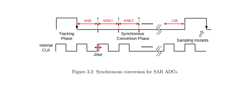
a clock running at least \((N + 1) \cdot
F_s\) is required for an \(N\)-bit converter with conversion rate of
\(F_s\)
every clock cycle has to tolerate the worst case comparison
time
every clock cycle requires margin for the clock jitter
The power and speed limitations of a synchronous SA design comes
largely from the high-speed internal clock
The comparator itself trigger the next bit-conversion cycle as soon
as the present bit decision has been taken
The maximum resolving time reduction between synchronous and
asynchronous case is two fold
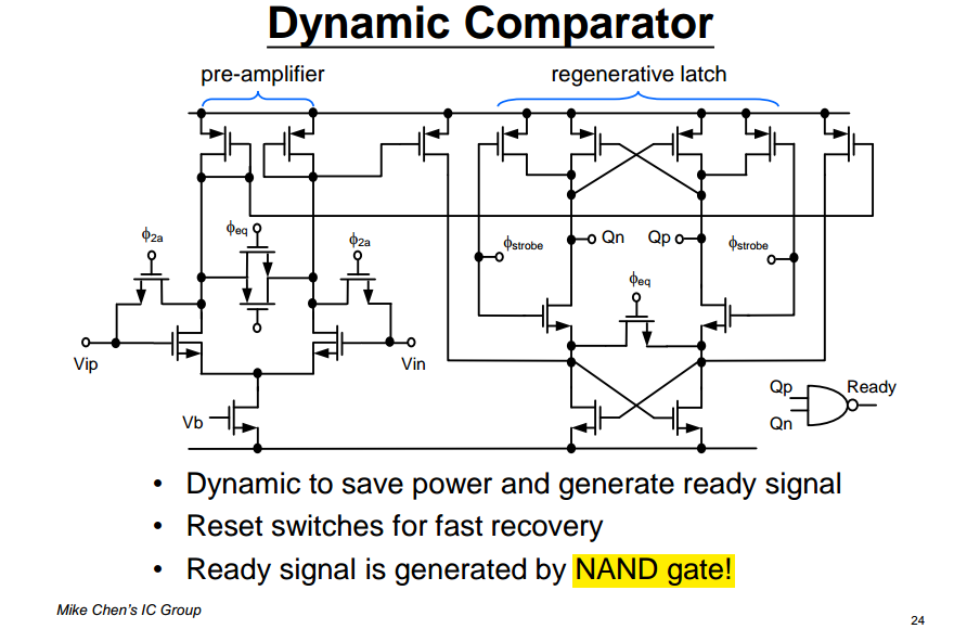
comparator metastable state
when the input is sufficiently small. The time needed for
the comparator outputs to fully resolve may take arbitrarily
long
In this case, the ready signal generator should still set the
flag and the decision result is simply taken from the previous
value stored in the SR latch
both outputs (\(Q_p\) and \(Q_n\)) will drop together, NAND is
inverter actually
The transition point of this NAND gate is skewed to
eliminate metastability issues arising when the input differential
voltage level is small (comparator)
reference
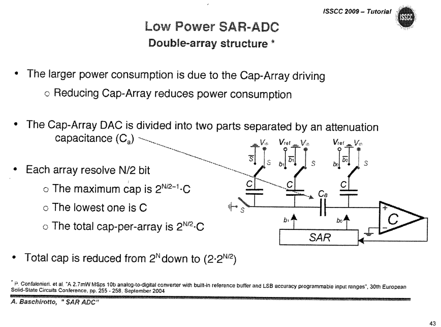
Andrea Baschirotto, "T6: SAR ADCs" ISSCC2009
Pieter Harpe, ISSCC 2016 Tutorial: "Basics of SAR ADCs Circuits &
Architectures"
Mike Shuo-Wei Chen and R. W. Brodersen, "A 6-bit 600-MS/s 5.3-mW
Asynchronous ADC in 0.13-μm CMOS," in IEEE Journal of Solid-State
Circuits, vol. 41, no. 12, pp. 2669-2680, Dec. 2006 [pdf,
slides]
C. -C. Liu, S. -J. Chang, G. -Y. Huang and Y. -Z. Lin, "A 10-bit
50-MS/s SAR ADC With a Monotonic Capacitor Switching Procedure," in
IEEE Journal of Solid-State Circuits, vol. 45, no. 4, pp.
731-740, April 2010 [https://sci-hub.se/10.1109/JSSC.2010.2042254]
L. Jie et al., "An Overview of Noise-Shaping SAR ADC: From
Fundamentals to the Frontier," in IEEE Open Journal of the Solid-State
Circuits Society, vol. 1, pp. 149-161, 2021 [pdf]
W. Liu, P. Huang and Y. Chiu, "A 12-bit, 45-MS/s, 3-mW Redundant
Successive-Approximation-Register Analog-to-Digital Converter With
Digital Calibration," in IEEE Journal of Solid-State Circuits, vol. 46,
no. 11, pp. 2661-2672, Nov. 2011 [https://sci-hub.st/10.1109/JSSC.2011.2163556]


.svg)